3/97
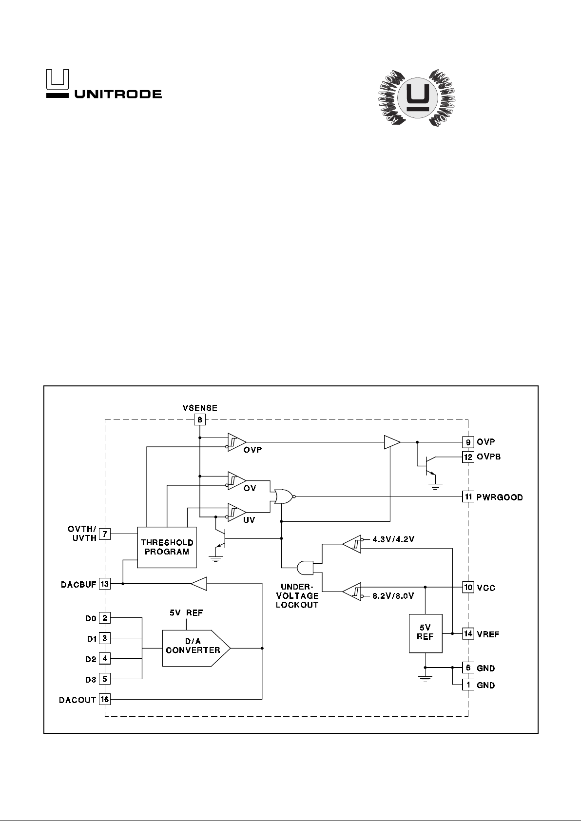
BLOCK DIAGRAM
• Precision 5V Reference
• 4-Bit Digital-to-Analog (DAC)
Converter
• 0.5% DAC/Reference Combined
Error
• Programmable Undervoltage and
Overvoltage Fault Windows
• Overvoltage Comparator with
Complementary SCR Driver and
Open Collector Outputs
• Undervoltage Lockout
The UC3910 is a com plete precision reference and voltage monitor circuit for Intel Pentium® Pro and other high-end microprocessor power
supplies. It is designed for use in conjunction with the UC3886 PWM. The
UC3910 together with the UC3886 converts 5VDC to an adjustable output ranging fr o m 2. 0V D C to 3 .5 V DC i n 10 0mV steps with 1% DC sy stem
accuracy.
The UC3910 utilizes thin film resistors to ensure high accuracy and stability of its precision circuits. The chip includes a precision 5V voltage reference which is capable of sourcing 10mA to external circuitry. The
output voltage of th e DAC is derived from this reference, and the accuracy of the DAC/reference combination is 0.5%. Programmable window
comparators monitor the supply voltage to indicate that it is within acceptable limits. The window is programmed as a percentage centered
around the DAC output. An overvoltage protection comparator is set at a
percentage 2 times large r than the programmed lower overvoltage level
and drives an external SCR as well as provides an open collector output.
Undervoltage lockout protection assures the correct logic states at the
outputs during power-up and power-down.
4-Bit DAC and Voltage Monitor
FEATURES DESCRIPTION
UC1910
UC2910
UC3910
UDG-95097-3

UC1910
UC2910
UC3910
PARAMETER TEST CONDITIONS MIN TYP MAX UNITS
Undervoltage Lockout
VIN UVLO Turn-on Threshold 7 8 9 V
UVLO Threshold Hysteresis 50 200 500 mV
Supply Current
I
IN
Startup VCC = 5V 2 3.5 mA
I
IN
VCC = 12V 10 12 mA
DAC/Reference
DACOUT Voltage Accuracy Line, Load, 0°C < T
A
< 70°C (Note 1)
−
0.9 0.9 %
Line, Load, –55°C < TA < 125°C –1.5 1.5 %
D0-D3 Voltage High D
X
Pin Floating 4.6 4.85 V
D0-D3 Input Bias Current D
X
Pin Tied to GND –140−105
µ
A
VREF Output Voltage I
VREF
= 0mA, 0°C < TA < 70°C 4.97 5 5.03 V
VREF Total Variation Line, Load, 0°C < TA < 70°C (Note 1) 4.96 5 5.04 V
Line, Load, –55°C < T
A
< 125°C 4.925 5 5.075 V
VREF Sourcing Current VREF = 0V 10 mA
DAC Buffer
Input Offset Voltage I
DACBUF
= –1mA, 0°C < TA < 70°C
−
25 25 mV
Output Sourcing Current –12 –1 mA
Monitor Circuitry (Note 2)
VSENSE UV Threshold Voltage Code 0, Ratio = 0.45 (Note 3) 3.174 3.237 3.3 V
Code 0, Ratio = 0.9 2.87 2.975 3.08 V
Code 15, Ratio = 0. 45 1.816 1.85 1.884 V
Code 15, Ratio = 0.9 1.635 1.7 1.765 V
VSENSE OV Threshold Voltage Code 0, Ratio = 0.45 3.7 3.763 3.826 V
Code 0, Ratio = 0.9 3.92 4.025 4.13 V
Code 15, Ratio = 0. 45 2.116 2.15 2.184 V
Code 15, Ratio = 0.9 1.635 2.3 2.365 V
ELECTRICAL CHARACTERISTICS
Unless otherwise specified, VCC = 12V, VSENSE = 3.5V, V
OVTH/UVTH
= 1.26V,
VD0 = VD1 = VD2 = VD3 = 0V, 0°C < TA < 70°C for the UC3910, –25°C < TA < 80°C for the UC2910, –55°C < TA < 125°C for the
UC1910 TA = TJ.
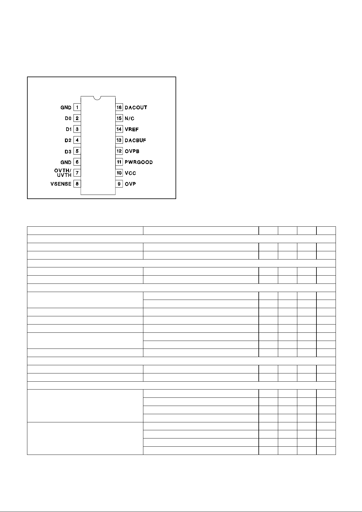
CONNECTION DIAGRAM
DIL-16, SOIC-16 (Top Vie w )
J, N, or D Packages
2
 Loading...