

3/97
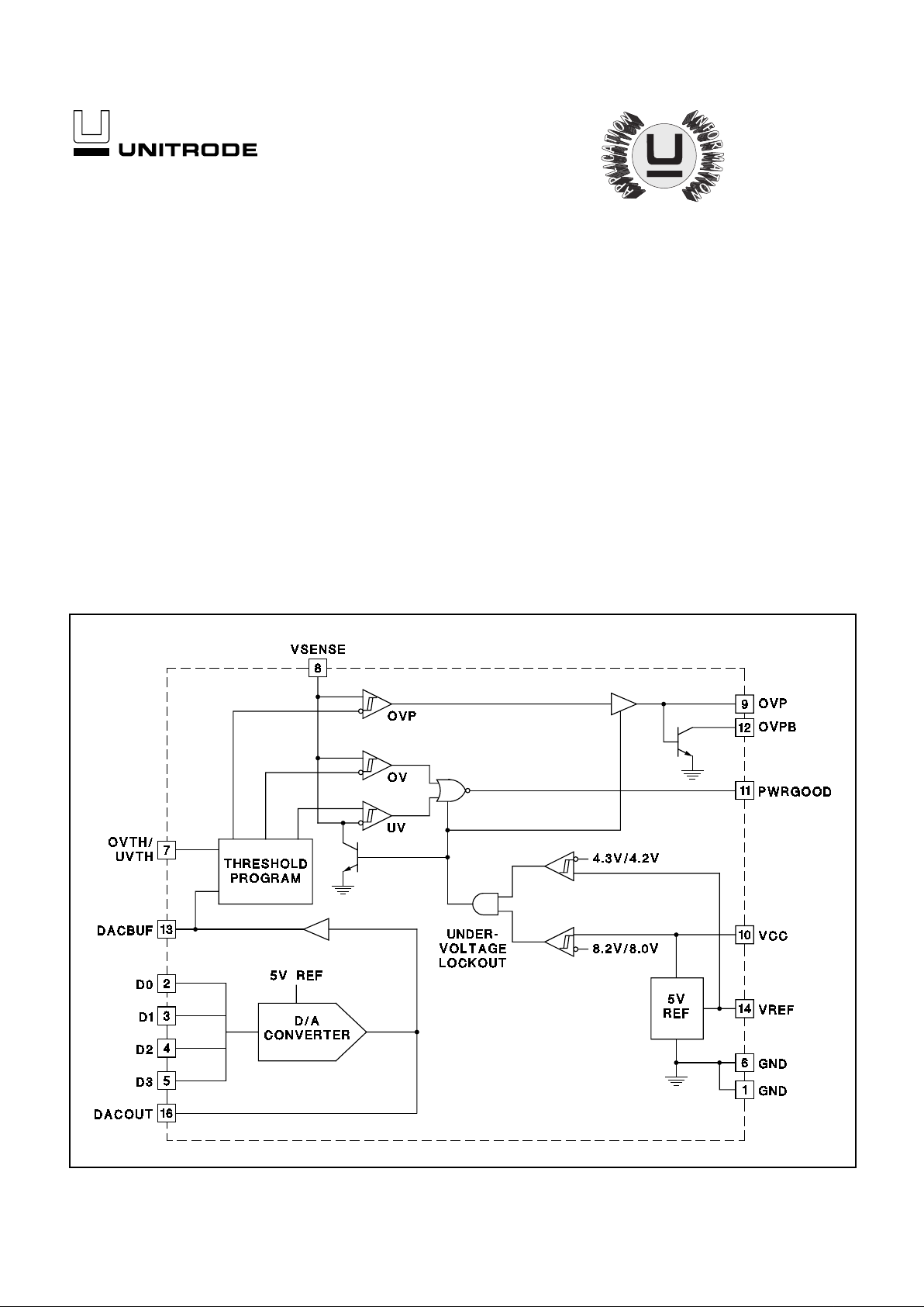
BLOCK DIAGRAM
• Precision 5V Reference
• 4-Bit Digital-to-Analog (DAC)
Converter
• 0.5% DAC/Reference Combined
Error
• Programmable Undervoltage and
Overvoltage Fault Windows
• Overvoltage Comparator with
Complementary SCR Driver and
Open Collector Outputs
• Undervoltage Lockout
The UC3910 is a com plete precision reference and voltage monitor circuit for Intel Pentium® Pro and other high-end microprocessor power
supplies. It is designed for use in conjunction with the UC3886 PWM. The
UC3910 together with the UC3886 converts 5VDC to an adjustable output ranging fr o m 2. 0V D C to 3 .5 V DC i n 10 0mV steps with 1% DC sy stem
accuracy.
The UC3910 utilizes thin film resistors to ensure high accuracy and stability of its precision circuits. The chip includes a precision 5V voltage reference which is capable of sourcing 10mA to external circuitry. The
output voltage of th e DAC is derived from this reference, and the accuracy of the DAC/reference combination is 0.5%. Programmable window
comparators monitor the supply voltage to indicate that it is within acceptable limits. The window is programmed as a percentage centered
around the DAC output. An overvoltage protection comparator is set at a
percentage 2 times large r than the programmed lower overvoltage level
and drives an external SCR as well as provides an open collector output.
Undervoltage lockout protection assures the correct logic states at the
outputs during power-up and power-down.
4-Bit DAC and Voltage Monitor
FEATURES DESCRIPTION
UC1910
UC2910
UC3910
UDG-95097-3
UC1910
UC2910
UC3910
PARAMETER TEST CONDITIONS MIN TYP MAX UNITS
Undervoltage Lockout
VIN UVLO Turn-on Threshold 7 8 9 V
UVLO Threshold Hysteresis 50 200 500 mV
Supply Current
I
IN
Startup VCC = 5V 2 3.5 mA
I
IN
VCC = 12V 10 12 mA
DAC/Reference
DACOUT Voltage Accuracy Line, Load, 0°C < T
A
< 70°C (Note 1)
−
0.9 0.9 %
Line, Load, –55°C < TA < 125°C –1.5 1.5 %
D0-D3 Voltage High D
X
Pin Floating 4.6 4.85 V
D0-D3 Input Bias Current D
X
Pin Tied to GND –140−105
µ
A
VREF Output Voltage I
VREF
= 0mA, 0°C < TA < 70°C 4.97 5 5.03 V
VREF Total Variation Line, Load, 0°C < TA < 70°C (Note 1) 4.96 5 5.04 V
Line, Load, –55°C < T
A
< 125°C 4.925 5 5.075 V
VREF Sourcing Current VREF = 0V 10 mA
DAC Buffer
Input Offset Voltage I
DACBUF
= –1mA, 0°C < TA < 70°C
−
25 25 mV
Output Sourcing Current –12 –1 mA
Monitor Circuitry (Note 2)
VSENSE UV Threshold Voltage Code 0, Ratio = 0.45 (Note 3) 3.174 3.237 3.3 V
Code 0, Ratio = 0.9 2.87 2.975 3.08 V
Code 15, Ratio = 0. 45 1.816 1.85 1.884 V
Code 15, Ratio = 0.9 1.635 1.7 1.765 V
VSENSE OV Threshold Voltage Code 0, Ratio = 0.45 3.7 3.763 3.826 V
Code 0, Ratio = 0.9 3.92 4.025 4.13 V
Code 15, Ratio = 0. 45 2.116 2.15 2.184 V
Code 15, Ratio = 0.9 1.635 2.3 2.365 V
ELECTRICAL CHARACTERISTICS
Unless otherwise specified, VCC = 12V, VSENSE = 3.5V, V
OVTH/UVTH
= 1.26V,
VD0 = VD1 = VD2 = VD3 = 0V, 0°C < TA < 70°C for the UC3910, –25°C < TA < 80°C for the UC2910, –55°C < TA < 125°C for the
UC1910 TA = TJ.
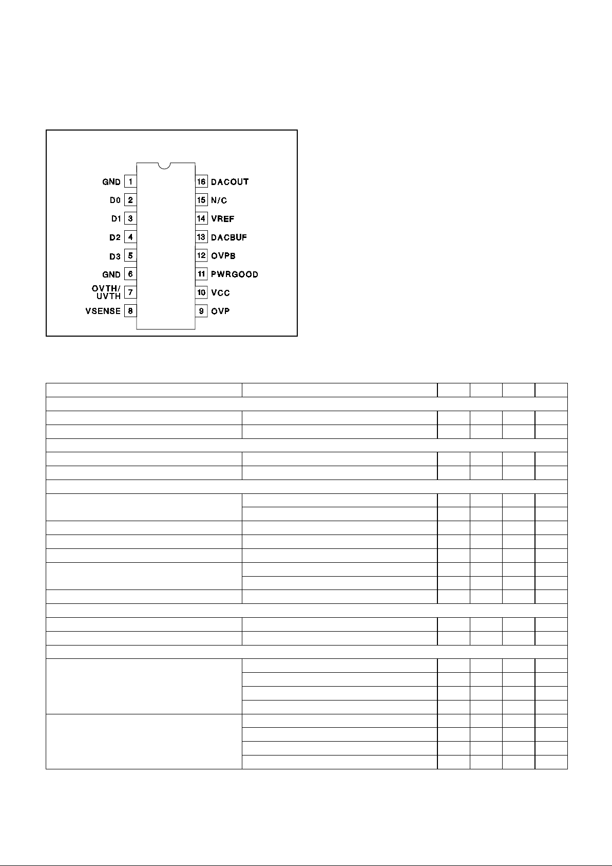
CONNECTION DIAGRAM
DIL-16, SOIC-16 (Top Vie w )
J, N, or D Packages
2

UC1910
UC2910
UC3910
PARAMETER TEST CONDITIONS MIN TYP MAX UNITS
Monitor Circuitry (Note 2) (cont.)
VSENSE OVP Threshold Voltage Code 0, Ratio = 0.45 3.937 4.025 4.113 V
Code 0, Ratio = 0.9 4.41 4.55 4.69 V
Code 15, Ratio = 0.45 2.235 2.3 2.365 V
Code 15, Ratio = 0.9 2.505 2.6 2.695 V
OV, UV Comparator Hysteresis Code 0, Ratio = 0.9 70 88 120 mV
Code 15, Ratio = 0.45 15 25 40 mV
OVP Comparator Hysteresis Code 0, Ratio = 0.9 160 218 300 mV
Code 15, Ratio = 0.45 40 62 85 mV
Input Common Mode Range OV, UV, OVP Comparators 0 5 V
Propagation Delay OV, UV Comparators 5
µ
s
OVP Comparator 5
µ
s
PWRGOOD, OVP, OVPB Outputs
PWRGOOD Voltage Low I
PWRGOOD
= 10mA 0.4 V
OVP Sourcing Current V
OVP
= 1.4V 65 mA
OVPB Voltage Low I
OVPB
= 1mA 0.4 V
ELECTRICAL CHARACTERISTICS (cont.)
Unless otherwise specifie d, VCC = 12V, VSENSE = 3.5 V, V
OVTH/UVTH
=
1.26V, VD0 = VD1 = VD2 = VD3 = 0V, 0°C < TA < 70°C for the UC3910, –25°C < TA < 80°C for the UC2910, –55°C < TA < 125°C for
the UC1910 TA = TJ.
D0-D3 (DAC Digital Input Control Codes):
These are
the DAC digital input control codes, with D0 representing th e least sig nificant bit (LSB) and D3, the most
significan t bit (MSB) (See Table 1). A bit is set low by
being connec ted to GND; a bit is set high by floating it,
or connecting it to a 3V to 5V voltage source. Each control pin is pulled up to ap pr oximate ly 4. 8V by an internal
40µA current source.
DACBUF (Buffered DACOUT Voltage):
This pin provides a buffered version of the DACOUT voltage to allow external programming of the OV/UV thresholds (see
OVTH/UVTH below).
DACOUT (Digital-to-Analog Converter Output Voltage):
This pin is the out put of the 4-bit digital to analog
(DAC) converter. Setting all input control codes low produces 3.5V at DACOUT; setting all codes high produces 2.0V at DACOUT. The LSB step size (i.e.
resolution) is 100mV (See Table 1). The DACOUT
source impe dance is typically 3kΩ and must therefore
drive a high impedance input. Bypass DACOUT at the
driven input with a 0.01µF, low ESR, low ESL capacitor
for best circuit noise immunity.
GND (Sig nal Ground):
All voltages are measured with
respect to GND. The two GND pins are connected together internally but should also be connected externally using a short PC bo ard trace. Bypass capacitors
on the VCC and VREF pins should be connected directly to the gr ound plane near one of the signal ground
PIN DESCRIPTIONS
Note 1: "Line, Load" implies that the parameter is tested at all combinations of the conditions:
10.8V < VCC < 13.2V, –2mA < I
VREF
< 0mA.
Note 2: These are the actual voltages on VSENSE which will cause the OVPB and PWRGOOD outputs to swi tch, assuming the
DACOUT voltage is perfect. These limits apply for 0°C < TA < 70°C.
Note 3: "Code 0" means pins D0 - D4 are all low; "Cod e 15 " me ans they are all fl oa ti ng or high (See Table 1). "Ratio" is the divider
ratio of the resistor string between DACBUF and OVTH/UVTH (See Figure 1).
Decimal
Code
D3 D2 D1 D0 DACOUT
Voltage
1511112.0
1411102.1
1311012.2
1211002.3
1110112.4
1010102.5
910012.6
810002.7
701112.8
601102.9
501013.0
401003.1
300113.2
200103.3
100013.4
000003.5
T ab le 1. Programming the DACOUT Voltage
3
pins.
OVP (Overvoltage Comparator Output):
This output
pin drives an external SCR circuit with up to 65mA
when the voltage on VSENSE rises above its nominal
value by a percentage set by the voltage on the
OVTH/UVTH pin (see below). The OVP comparator hysteresis is a function of both the DACBUF voltage and
the OV/UV percentage programmed.
OVPB (Overvoltage Comparator Complementary
Output):
This output is a complement to th e OVP output (see above) and provides an open collector capable
of sinking 1mA when the voltage on VSENSE rises
above its nominal value by a percentage set by the voltage on the OVTH/UVTH pin (see below).
OVTH/UVTH (Undervoltage and Lower Overvoltage
Threshold Input):
This pin is us ed to program the window thresholds for the OV and UV comparators. The
OV- U V wi nd ow is c e nt ered ar ound the DACBUF voltage
and can be programmed from ±5% to ±15% about
DACBUF. Connect a resistor divider between DACBUF
and GND to set the percentage. The threshold for the
OVP comparator is internally set to a percentage 2
times larger than the programmed OV percentage;
therefore, its range extends from 10% to 30% above
DACBUF.
PWRGOOD (Undervoltage/Lower Overvoltage Out-
put):
This pin is an open collector output which is
driven low to rese t the microprocessor when VSENSE
rises above or falls below its nominal value by a percentage pro grammed by OVTH/UVTH. The OV and UV
comparators’ hysteresis is a function of the DACBUF
voltage and the OV/UV programmed percentage.
VCC (Positive Supply Voltage):
This pin supplies
power to the chip. Connect VCC to a stable voltage
source of at least 9V and ca pable of sourcing at least
15mA. The OVP and PWRGOOD outputs are held low,
the OVPB output is in a high impedance state, and the
VSENSE pin is pulled low until VCC exceeds the upper
undervolta ge lockout threshold. This pin should be bypassed direc tly to the GND pin with a 0.1µF low ESR,
low ESL capacitor.
VREF (Voltage Reference Output):
This pin provides
an accurate 5V reference, capable of delivering up to
10mA to exter nal cir cuitr y, and is internally shor t circuit
current limited. For best reference stability, bypass
VREF directly to the GND pin with a 0.1µF, low ESR,
low ESL capacitor.
VSENSE (Output Voltage Sensing Input):
This pin is
the input to the OVP and PWRGOOD comparators and
is connected to the system output voltage through a
lowpass filter. When choosing the resistor value for this
filter, make sure that no more than 500µA will flow
PIN DESCRIPTIONS (cont.)
UC1910
UC2910
UC3910
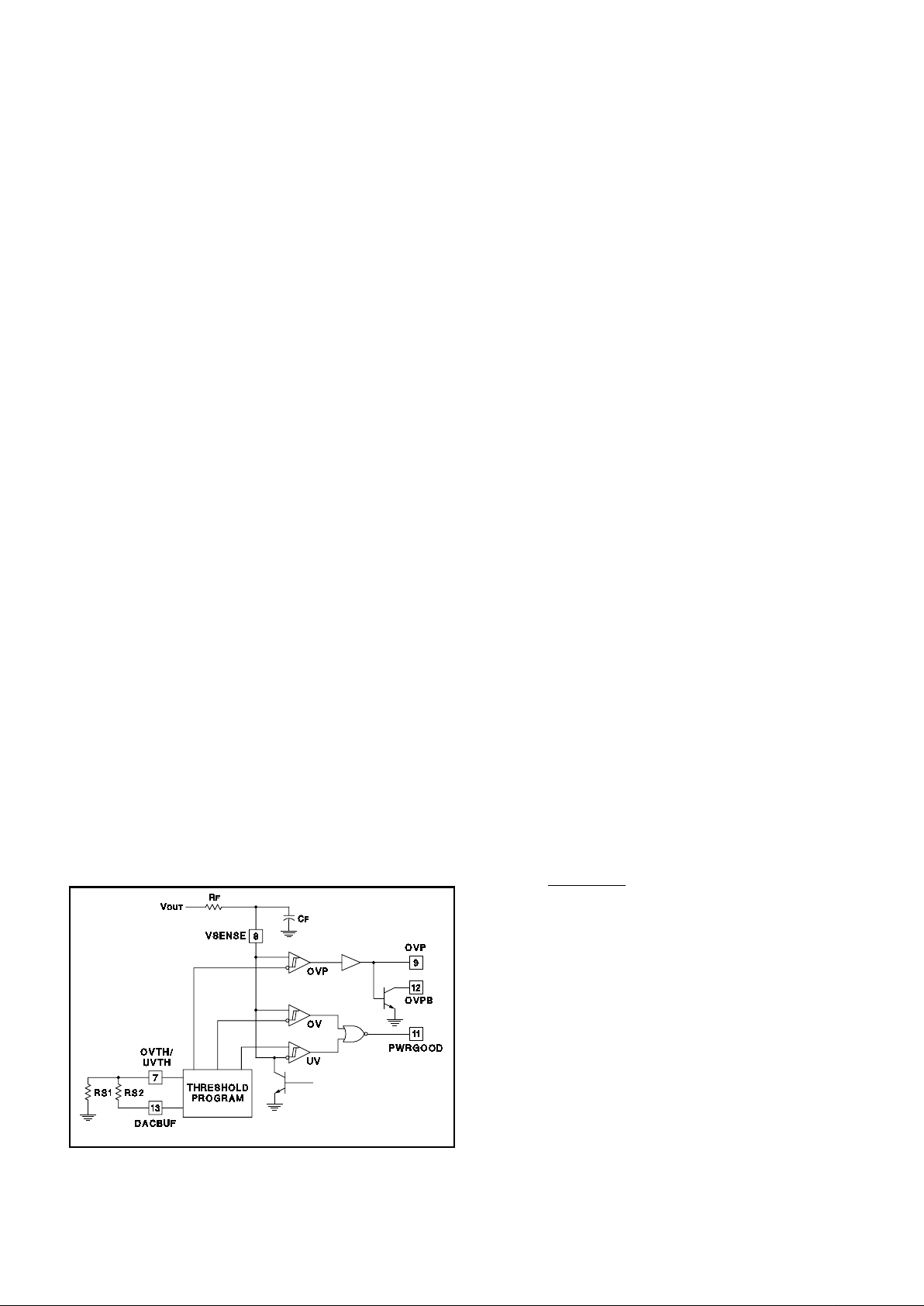
APPLICATION INFORMATION
The Overvoltage ( OV), Undervoltage (UV) and Overvoltage Protection Voltage (OVP) threshold detection voltages are programmed as a percentage about the
nominal DAC output voltage, DACOUT. Figure 1 illus-
trates how to program the UC3910 by setting a voltage
divider, R
DIV
, at the OVTH/UVTH pin. The voltage di-
vider ratio is defined as
R
DIV
=
RS1
RS1 + RS2
The UC3910 a llows a ratio R
DIV
at the OVTH/UVTH pin
from 0.3 to 0.9, which cor responds to overvoltage and
undervoltage percentage thresholds from 5% to 15%
and an OVP percentage threshold from 10% to 30%.
These thresholds are shown in Figure 2.
The OV, UV and OVP percentage thresholds are given
by
%V
OV
= R
DIV
• 16.7
%V
UV
= –(R
DIV
• 16.7)
%V
OVP
= %VOV • 2.0 = R
DIV
• 33.4
An R-C filter is added to the VSENSE pin to filter noise
and ripple at the comparator inputs. An R-C filter frequency of F
SWITCH
/10 is recommended. Choose the
Figure 1. Setting the OV/UV/O VP Threshold
Percentages
UDG-96020
4

UNITRODE CORPORATION
7 CONTINENTAL BLVD. • MERRIMACK, NH 03054
TEL. (603) 424-2410 • FAX (603) 424-3460
value of RF such that it limits the current into VSENSE
to ≤ 0.5mA.
R
F
• CF =
1
2
• π •
F
SWITCH
10
R
F
≥
V
OUT
0.5mA
The Overvoltage Protection output, OVP, can be used
to directly dr i ve a crowba rr ing S CR, as s hown i n Figure
3.
A typical application is shown in Figure 4 using the
UC3910 together with the UC3886 Average Current
Mode PWM Co nt roller IC for a power supply to drive Intel’s Pentium®Pro processor.
-15
-10
-5
0
5
10
15
20
25
30
0.3 0.4 0.5 0.6 0.7 0.8 0.9
Ratio R
DIV
Thresholds (%)
UV
OV
OVP
Figure 2. OV, UV and O VP Percentage Thresholds as a
Function of the Divider Ratio R
DIV
UC1910
UC2910
UC3910
Figure 3. Driving and SCR Using the UC3910 OVP
Signal
Figure 4. UC3910 Configured with the UC3886 for a Pentium® Pro DC/DC Co nverter
APPLICATION INFORMATION (cont.)
UDG-96021
UDG-96019
5

IMPORTANT NOTICE
T exas Instruments and its subsidiaries (TI) reserve the right to make changes to their products or to discontinue
any product or service without notice, and advise customers to obtain the latest version of relevant information
to verify, before placing orders, that information being relied on is current and complete. All products are sold
subject to the terms and conditions of sale supplied at the time of order acknowledgement, including those
pertaining to warranty, patent infringement, and limitation of liability.
TI warrants performance of its semiconductor products to the specifications applicable at the time of sale in
accordance with TI’s standard warranty. Testing and other quality control techniques are utilized to the extent
TI deems necessary to support this warranty. Specific testing of all parameters of each device is not necessarily
performed, except those mandated by government requirements.
CERT AIN APPLICATIONS USING SEMICONDUCTOR PRODUCTS MAY INVOLVE POTENTIAL RISKS OF
DEATH, PERSONAL INJURY, OR SEVERE PROPERTY OR ENVIRONMENTAL DAMAGE (“CRITICAL
APPLICATIONS”). TI SEMICONDUCTOR PRODUCTS ARE NOT DESIGNED, AUTHORIZED, OR
WARRANTED TO BE SUITABLE FOR USE IN LIFE-SUPPORT DEVICES OR SYSTEMS OR OTHER
CRITICAL APPLICATIONS. INCLUSION OF TI PRODUCTS IN SUCH APPLICA TIONS IS UNDERSTOOD T O
BE FULLY AT THE CUSTOMER’S RISK.
In order to minimize risks associated with the customer’s applications, adequate design and operating
safeguards must be provided by the customer to minimize inherent or procedural hazards.
TI assumes no liability for applications assistance or customer product design. TI does not warrant or represent
that any license, either express or implied, is granted under any patent right, copyright, mask work right, or other
intellectual property right of TI covering or relating to any combination, machine, or process in which such
semiconductor products or services might be or are used. TI’s publication of information regarding any third
party’s products or services does not constitute TI’s approval, warranty or endorsement thereof.
Copyright 1999, Texas Instruments Incorporated
 Loading...