

Texas Instruments THS8200PFP, THS8200 Datasheet

October 2002 DAV Digital Video/Imaging
Data Manual
SLES032A

IMPORTANT NOTICE
Texas Instruments Incorporated and its subsidiaries (TI) reserve the right to make corrections, modifications,
enhancements, improvements, and other changes to its products and services at any time and to discontinue
any product or service without notice. Customers should obtain the latest relevant information before placing
orders and should verify that such information is current and complete. All products are sold subject to TI’s terms
and conditions of sale supplied at the time of order acknowledgment.
TI warrants performance of its hardware products to the specifications applicable at the time of sale in
accordance with TI’s standard warranty . Testing and other quality control techniques are used to the extent TI
deems necessary to support this warranty. Except where mandated by government requirements, testing of all
parameters of each product is not necessarily performed.
TI assumes no liability for applications assistance or customer product design. Customers are responsible for
their products and applications using TI components. T o minimize the risks associated with customer products
and applications, customers should provide adequate design and operating safeguards.
TI does not warrant or represent that any license, either express or implied, is granted under any TI patent right,
copyright, mask work right, or other TI intellectual property right relating to any combination, machine, or process
in which TI products or services are used. Information published by TI regarding third–party products or services
does not constitute a license from TI to use such products or services or a warranty or endorsement thereof.
Use of such information may require a license from a third party under the patents or other intellectual property
of the third party, or a license from TI under the patents or other intellectual property of TI.
Reproduction of information in TI data books or data sheets is permissible only if reproduction is without
alteration and is accompanied by all associated warranties, conditions, limitations, and notices. Reproduction
of this information with alteration is an unfair and deceptive business practice. TI is not responsible or liable for
such altered documentation.
Resale of TI products or services with statements different from or beyond the parameters stated by TI for that
product or service voids all express and any implied warranties for the associated TI product or service and
is an unfair and deceptive business practice. TI is not responsible or liable for any such statements.
Mailing Address:
Texas Instruments
Post Office Box 655303
Dallas, Texas 75265
Copyright 2002, Texas Instruments Incorporated

iii
Contents
Section Title Page
1 Introduction 1–1. . . . . . . . . . . . . . . . . . . . . . . . . . . . . . . . . . . . . . . . . . . . . . . . . . . . . .
1.1 Description 1–1. . . . . . . . . . . . . . . . . . . . . . . . . . . . . . . . . . . . . . . . . . . . . . . . .
1.2 Features 1–1. . . . . . . . . . . . . . . . . . . . . . . . . . . . . . . . . . . . . . . . . . . . . . . . . . .
2 Terminal Descriptions 2–1. . . . . . . . . . . . . . . . . . . . . . . . . . . . . . . . . . . . . . . . . . . . .
3 THS8200 Functional Overview 3–1. . . . . . . . . . . . . . . . . . . . . . . . . . . . . . . . . . . . .
3.1 Data Manager (DMAN) 3–1. . . . . . . . . . . . . . . . . . . . . . . . . . . . . . . . . . . . . . .
3.1.1 Interpolating Finite Impulse Responses Filter (IFIR) 3–2. . . . .
3.1.2 Color-Space Conversion (CSC) 3–2. . . . . . . . . . . . . . . . . . . . . . .
3.1.3 Clip/Shift/Multiplier (CSM) 3–2. . . . . . . . . . . . . . . . . . . . . . . . . . . .
3.1.4 Digital Multiplexer (DIGMUX) 3–2. . . . . . . . . . . . . . . . . . . . . . . . .
3.1.5 Display Timing Generator (DTG) 3–2. . . . . . . . . . . . . . . . . . . . . .
3.1.6 Clock Generator (CGEN) 3–3. . . . . . . . . . . . . . . . . . . . . . . . . . . .
3.1.7 Clock Driver (CDRV) 3–3. . . . . . . . . . . . . . . . . . . . . . . . . . . . . . . .
3.1.8 I
2
C Host Interface (I2CSLAVE) 3–3. . . . . . . . . . . . . . . . . . . . . . .
3.1.9 Test Block (TST) 3–3. . . . . . . . . . . . . . . . . . . . . . . . . . . . . . . . . . . .
3.1.10 D/A Converters (DAC) 3–3. . . . . . . . . . . . . . . . . . . . . . . . . . . . . . .
4 Detailed Functional Description 4–1. . . . . . . . . . . . . . . . . . . . . . . . . . . . . . . . . . . .
4.1 Data Manager (DMAN) 4–1. . . . . . . . . . . . . . . . . . . . . . . . . . . . . . . . . . . . . . .
4.2 Input Interface Formats 4–2. . . . . . . . . . . . . . . . . . . . . . . . . . . . . . . . . . . . . .
4.3 Clock Generator (CGEN)/Clock Driver (CDRV) 4–5. . . . . . . . . . . . . . . . . .
4.4 Color Space Conversion (CSC) 4–6. . . . . . . . . . . . . . . . . . . . . . . . . . . . . . .
4.5 Clip/Scale/Multiplier (CSM) 4–8. . . . . . . . . . . . . . . . . . . . . . . . . . . . . . . . . . .
4.5.1 Clipping 4–8. . . . . . . . . . . . . . . . . . . . . . . . . . . . . . . . . . . . . . . . . . .
4.5.2 Shifting 4–9. . . . . . . . . . . . . . . . . . . . . . . . . . . . . . . . . . . . . . . . . . . .
4.5.3 Multiplying 4–10. . . . . . . . . . . . . . . . . . . . . . . . . . . . . . . . . . . . . . . . .
4.6 Interpolating Finite Impulse Response Filter (IFIR) 4–11. . . . . . . . . . . . . . .
4.7 Display Timing Generator (DTG) 4–14. . . . . . . . . . . . . . . . . . . . . . . . . . . . . .
4.7.1 Overview of Functionality 4–14. . . . . . . . . . . . . . . . . . . . . . . . . . . .
4.7.2 Functional Description 4–15. . . . . . . . . . . . . . . . . . . . . . . . . . . . . . .
4.7.3 DTG Line Type Overview 4–19. . . . . . . . . . . . . . . . . . . . . . . . . . . .
4.8 D/A Conversion 4–35. . . . . . . . . . . . . . . . . . . . . . . . . . . . . . . . . . . . . . . . . . . . .
4.8.1 RGB Output Without Sync Signal Insertion/
General-Purpose Application DAC 4–35. . . . . . . . . . . . . . . . . . . .
4.8.2 SMPTE-Compatible RGB Output With Sync
Signal Inserted on G (Green) Channel 4–36. . . . . . . . . . . . . . . . .
4.8.3 SMPTE-Compatible Analog-Level Output With
Sync Inserted on All RGB Channels 4–38. . . . . . . . . . . . . . . . . . .
4.8.4 SMPTE-Compatible YPbPr Output With
Sync Signal Inserted on Y Channel Only 4–38. . . . . . . . . . . . . . .

iv
4.8.5 SMPTE-Compatible YPbPr Output With Sync Signal
Inserted on All Channels 4–39. . . . . . . . . . . . . . . . . . . . . . . . . . . . .
4.8.6 Summary of Supported Video Formats 4–40. . . . . . . . . . . . . . . .
4.9 Test Functions 4–40. . . . . . . . . . . . . . . . . . . . . . . . . . . . . . . . . . . . . . . . . . . . . .
4.10 Power Down 4–40. . . . . . . . . . . . . . . . . . . . . . . . . . . . . . . . . . . . . . . . . . . . . . . .
4.11 CGMS Insertion 4–40. . . . . . . . . . . . . . . . . . . . . . . . . . . . . . . . . . . . . . . . . . . . .
4.12 I
2
C Interface 4–41. . . . . . . . . . . . . . . . . . . . . . . . . . . . . . . . . . . . . . . . . . . . . . . .
5I
2
C Register Map 5–1. . . . . . . . . . . . . . . . . . . . . . . . . . . . . . . . . . . . . . . . . . . . . . . . . .
5.1 Register Descriptions 5–6. . . . . . . . . . . . . . . . . . . . . . . . . . . . . . . . . . . . . . . .
5.1.1 System Control (Sub-Addresses 0x02–0x03) 5–6. . . . . . . . . . .
5.1.2 Color Space Conversion Control
(Sub-Addresses 0x04–0x19) 5–8. . . . . . . . . . . . . . . . . . . . . . . . .
5.1.3 Test Control (Sub-Addresses 0x1A–0x1B) 5–10. . . . . . . . . . . . .
5.1.4 Data Path Control (Sub-Address 0x1C) 5–10. . . . . . . . . . . . . . . .
5.1.5 Display Timing Generator Control, Part 1
(Sub-Addresses 0x1D–0x3C) 5–11. . . . . . . . . . . . . . . . . . . . . . . .
5.1.6 DAC Control (Sub-Addresses 0x3D–0x40) 5–14. . . . . . . . . . . . .
5.1.7 Clip/Scale/Multiplier Control (Sub-Addresses
0x41–0x4F) 5–15. . . . . . . . . . . . . . . . . . . . . . . . . . . . . . . . . . . . . . . .
5.1.8 Display Timing Generator Control, Part 2
(Sub-Addresses 0x50–0x82) 5–17. . . . . . . . . . . . . . . . . . . . . . . . .
5.1.9 CGMS Control (Sub-Addresses 0x83–0x85) 5–20. . . . . . . . . . . .
5.2 THS8200 Preset Mode Line Type Definitions 5–20. . . . . . . . . . . . . . . . . . . .
5.2.1 SMPTE_274P (1080p) 5–21. . . . . . . . . . . . . . . . . . . . . . . . . . . . . .
5.2.2 274M Interlaced (1080I) 5–21. . . . . . . . . . . . . . . . . . . . . . . . . . . . .
5.2.3 296M Progressive (720p) 5–21. . . . . . . . . . . . . . . . . . . . . . . . . . . .
5.2.4 SDTV 525 Interlaced Mode 5–22. . . . . . . . . . . . . . . . . . . . . . . . . .
5.2.5 SDTV 525 Progressive Mode 5–22. . . . . . . . . . . . . . . . . . . . . . . . .
5.2.6 SDTV 625 Interlaced Mode 5–23. . . . . . . . . . . . . . . . . . . . . . . . . .
6 Application Information 6–1. . . . . . . . . . . . . . . . . . . . . . . . . . . . . . . . . . . . . . . . . . .
6.1 Video vs Computer Graphics Application 6–1. . . . . . . . . . . . . . . . . . . . . . .
6.2 DVI to Analog YPbPr/RGB Application 6–1. . . . . . . . . . . . . . . . . . . . . . . . .
6.3 Master vs Slave Timing Modes 6–2. . . . . . . . . . . . . . . . . . . . . . . . . . . . . . . .
7 Specifications 7–1. . . . . . . . . . . . . . . . . . . . . . . . . . . . . . . . . . . . . . . . . . . . . . . . . . . .
7.1 Absolute Maximum Ratings Over Operating Free-Air
Temperature Range 7–1. . . . . . . . . . . . . . . . . . . . . . . . . . . . . . . . . . . . . . . . . .
7.2 Recommended Operating Conditions Over Operating
Free-Air Temperature Range, T
A
7–1. . . . . . . . . . . . . . . . . . . . . . . . . . . . . .
7.2.1 Power Supply 7–1. . . . . . . . . . . . . . . . . . . . . . . . . . . . . . . . . . . . . .
7.2.2 Digital and Reference Inputs 7–1. . . . . . . . . . . . . . . . . . . . . . . . .
7.3 Electrical Characteristics Over Recommended Operating
Conditions With f
CLK
= 205 MHz and RFS = R
FS(nom)
7–2. . . . . . . . . . .
7.3.1 Power Supply, 1-MHz FS Ramp Simultaneously Applied
to All Three Channels 7–2. . . . . . . . . . . . . . . . . . . . . . . . . . . . . . .
7.3.2 Digital Inputs—DC Characteristics 7–3. . . . . . . . . . . . . . . . . . . .
7.3.3 Analog (DAC) Outputs 7–4. . . . . . . . . . . . . . . . . . . . . . . . . . . . . . .

v
7.4 Power Requirements 7–5. . . . . . . . . . . . . . . . . . . . . . . . . . . . . . . . . . . . . . . . .
7.4.1 Power for 700 mV DAC Output Compliance + 350 mV Bias
at AVDD = 3.3V, DVDD = 1.8V, VDD_IO = 3.3 V,
VDD_DLL = 3.3 V, 1-MHz Tone on All Channels 7–5. . . . . . . .
7.4.2 Power for 700 mV DAC Output Compliance + 350 mV Bias
at AVDD = 3.3V, DVDD = 1.8 V, VDD_IO = 1.8V,
VDD_DLL = 3.3V, 1-MHz Tone on All Channels 7–6. . . . . . . . .
7.4.3 Power for 1.25V Output Compliance Without Bias at
AVDD = 3.3 V, DVDD = 1.8 V, VDD_IO = 3.3 V,
VDD_DLL = 3.3 V, 1-MHz Tone on All Channels 7–7. . . . . . . .
7.4.4 Power for 1.25V Without Bias at AVDD = 3.3 V,
DVDD = 1.8 V, VDD_IO = 1.8 V, VDD_DLL = 3.3 V,
1-MHz Tone on All Channels 7–8. . . . . . . . . . . . . . . . . . . . . . . . .
7.5 Nonlinearity 7–9. . . . . . . . . . . . . . . . . . . . . . . . . . . . . . . . . . . . . . . . . . . . . . . . .
7.5.1 Differential Nonlinearity (DNL) and Integral
Nonlinearity (INL) for 700 mV Without Bias 7–9. . . . . . . . . . . . .
7.5.2 Differential Nonlinearity (DNL) and Integral
Nonlinearity (INL) for 700 mV + 350 mV Bias 7–10. . . . . . . . . . .
7.5.3 Differential Nonlinearity (DNL) and Integral
Nonlinearity (INL) for 1.25 V Without Bias 7–11. . . . . . . . . . . . . .
7.6 Analog Output Bandwidth (sinx/x corrected) at f
S
= 205 MSPS 7–12. . . .
7.7 Output Compliance vs Full-Scale Adjustment Resistor Value 7–12. . . . . .
7.8 Vertical Sync of the HDTV 1080I Format Preset in First and Second
Field, and Horizontal Line Waveform Detail 7–13. . . . . . . . . . . . . . . . . . . . .
8 Mechanical Information 8–1. . . . . . . . . . . . . . . . . . . . . . . . . . . . . . . . . . . . . . . . . . .

vi
List of Illustrations
Figure Title Page
2–1 THS8200 Pin Location Diagram 2–1. . . . . . . . . . . . . . . . . . . . . . . . . . . . . . . . . . . .
3–1 Functional Block Diagram 3–1. . . . . . . . . . . . . . . . . . . . . . . . . . . . . . . . . . . . . . . . . .
4–1 24-/30-Bit RGB or YCbCr Data Format 4–2. . . . . . . . . . . . . . . . . . . . . . . . . . . . . .
4–2 20-/16-Bit YCbCr 4:2:2 Data Format (16-Bit Operation Shown) 4–3. . . . . . . . . .
4–3 16-Bit RGB 4:4:4 Data Format 4–4. . . . . . . . . . . . . . . . . . . . . . . . . . . . . . . . . . . . . .
4–4 15-Bit RGB 4:4:4 Data Format 4–5. . . . . . . . . . . . . . . . . . . . . . . . . . . . . . . . . . . . . .
4–5 Effect of Clipping on Analog Output 4–9. . . . . . . . . . . . . . . . . . . . . . . . . . . . . . . . .
4–6 Effect of Shifting on Clipped Analog Output 4–9. . . . . . . . . . . . . . . . . . . . . . . . . . .
4–7 Effect of Scaling the Analog Video Output 4–10. . . . . . . . . . . . . . . . . . . . . . . . . . . .
4–8P
B
and PR Filter Requirements Based on SMPTE 296M/274M 4–11. . . . . . . . .
4–9 Y and RGB Filter Requirements Based on SMPTE 296M/274M 4–12. . . . . . . . .
4–10 Y and RGB Filter Requirements Based on ITU-R.BT601 4–12. . . . . . . . . . . . . .
4–11 Cb and Cr Filter Requirements Based on ITU-R.BT601 4–13. . . . . . . . . . . . . . .
4–12 IFIR Frequency Response 4–13. . . . . . . . . . . . . . . . . . . . . . . . . . . . . . . . . . . . . . . .
4–13 IFIR Pass-Band Frequency Response 4–13. . . . . . . . . . . . . . . . . . . . . . . . . . . . . .
4–14 IFIR Phase Response 4–14. . . . . . . . . . . . . . . . . . . . . . . . . . . . . . . . . . . . . . . . . . . .
4–15 THS8200 DTG VS/HS Output Generation 4–18. . . . . . . . . . . . . . . . . . . . . . . . . . .
4–16 Tri-Level Line-Synchronizing Signal Waveform 4–20. . . . . . . . . . . . . . . . . . . . . .
4–17 THS8200 VBI Line Types in HDTV Mode 4–21. . . . . . . . . . . . . . . . . . . . . . . . . . .
4–18 HDTV Line Type ACTIVE_VIDEO 4–22. . . . . . . . . . . . . . . . . . . . . . . . . . . . . . . . . .
4–19 HDTV Line Type FULL_NSTP 4–22. . . . . . . . . . . . . . . . . . . . . . . . . . . . . . . . . . . . .
4–20 HDTV Line Type NTSP_NTSP 4–23. . . . . . . . . . . . . . . . . . . . . . . . . . . . . . . . . . . . .
4–21 HDTV Line Type BTSP_BTSP 4–23. . . . . . . . . . . . . . . . . . . . . . . . . . . . . . . . . . . . .
4–22 HDTV Line Type NTSP_BTSP 4–24. . . . . . . . . . . . . . . . . . . . . . . . . . . . . . . . . . . . .
4–23 HDTV Line Type BTSP_NTSP 4–24. . . . . . . . . . . . . . . . . . . . . . . . . . . . . . . . . . . . .
4–24 HDTV Line Type FULL_BTSP 4–25. . . . . . . . . . . . . . . . . . . . . . . . . . . . . . . . . . . . .
4–25 Field/Frame Synchronizing Signal Waveform (1080I and
1080P Formats) 4–26. . . . . . . . . . . . . . . . . . . . . . . . . . . . . . . . . . . . . . . . . . . . . . . .
4–26 Horizontal Synchronization Signal Waveform 4–27. . . . . . . . . . . . . . . . . . . . . . . .
4–27 THS8200 VBI Line Types in SDTV Mode 4–28. . . . . . . . . . . . . . . . . . . . . . . . . . .
4–28 SDTV Line Type NEQ_NEQ 4–29. . . . . . . . . . . . . . . . . . . . . . . . . . . . . . . . . . . . . . .
4–29 SDTV Line Type FULL_BSP 4–29. . . . . . . . . . . . . . . . . . . . . . . . . . . . . . . . . . . . . .
4–30 SDTV Line Type BSP_BSP 4–30. . . . . . . . . . . . . . . . . . . . . . . . . . . . . . . . . . . . . . .

vii
4–31 SDTV Line Type FULL_NSP 4–30. . . . . . . . . . . . . . . . . . . . . . . . . . . . . . . . . . . . . .
4–32 SDTV Line Type NEQ_BSP 4–31. . . . . . . . . . . . . . . . . . . . . . . . . . . . . . . . . . . . . . .
4–33 SDTV Line Type BSP_NEQ 4–31. . . . . . . . . . . . . . . . . . . . . . . . . . . . . . . . . . . . . . .
4–34 SDTV Line Type FULL_NEQ 4–32. . . . . . . . . . . . . . . . . . . . . . . . . . . . . . . . . . . . . .
4–35 SDTV Line Type NSP_ACTIVE 4–32. . . . . . . . . . . . . . . . . . . . . . . . . . . . . . . . . . . .
4–36 SDTV Line Type ACTIVE_NEQ 4–33. . . . . . . . . . . . . . . . . . . . . . . . . . . . . . . . . . . .
4–37 SDTV Line Type ACTIVE_VIDEO 4–33. . . . . . . . . . . . . . . . . . . . . . . . . . . . . . . . . .
4–38 Field/Frame Synchronizing Signal Waveform (525I Format) 4–34. . . . . . . . . . .
4–39 RGB Without Sync Insertion or Composite Video Output 4–36. . . . . . . . . . . . . .
4–40 Ramping Output With Different Full-Scale Ranges 4–36. . . . . . . . . . . . . . . . . . .
4–41 G-Channel Output Waveform 4–37. . . . . . . . . . . . . . . . . . . . . . . . . . . . . . . . . . . . . .
4–42 R- and B-Channel Output Waveform 4–37. . . . . . . . . . . . . . . . . . . . . . . . . . . . . . .
4–43 R-, G-, and B-Channel Output Waveform 4–38. . . . . . . . . . . . . . . . . . . . . . . . . . .
4–44 Y-Channel Output Waveform 4–38. . . . . . . . . . . . . . . . . . . . . . . . . . . . . . . . . . . . . .
4–45 Analog Output of Cr and Cb Channels Without Sync Insertion 4–39. . . . . . . . .
4–46 Analog Output of Cr and Cb Channels With Sync Insertion 4–39. . . . . . . . . . . .
6–1 Typical Video Application 6–1. . . . . . . . . . . . . . . . . . . . . . . . . . . . . . . . . . . . . . . . . .
6–2 Computer Graphics Application 6–1. . . . . . . . . . . . . . . . . . . . . . . . . . . . . . . . . . . . .
6–3 Slave Operation Mode of THS8200 6–2. . . . . . . . . . . . . . . . . . . . . . . . . . . . . . . . .
6–4 Master Operation Mode of THS8200 6–3. . . . . . . . . . . . . . . . . . . . . . . . . . . . . . . .
7–1 THS8200 Output Waveforms for 1080I: Vertical Blanking in First and
Second Fields, and Active Video 7–13. . . . . . . . . . . . . . . . . . . . . . . . . . . . . . . . . .
List of Tables
Table Title Page
2–1 Terminal Functions 2–2. . . . . . . . . . . . . . . . . . . . . . . . . . . . . . . . . . . . . . . . . . . . . . . .
4–1 Supported Input Formats 4–1. . . . . . . . . . . . . . . . . . . . . . . . . . . . . . . . . . . . . . . . . .

1–1
1 Introduction
1.1 Description
THS8200 is a complete video back-end D/A solution for DVD players, personal video recorders and set-top boxes,
or any system requiring the conversion of digital component video signals into the analog domain.
THS8200 can accept a variety of digital input formats, in both 4:4:4 and 4:2:2 formats, over a 3 ×10-bit, 2 ×10-bit or
1 ×10-bit interface. The device synchronizes to incoming video data either through dedicated Hsync/Vsync inputs
or through extraction of the sync information from embedded sync (SAV/EAV) codes inside the video stream.
Alternatively , when configured for generating PC graphics output, THS8200 also provides a master timing mode in
which it requests video data from an external (memory) source.
THS8200 contains a display timing generator that is completely programmable for all standard and nonstandard
video formats up to the maximum supported pixel clock of 205 MSPS. Therefore, the device supports all component
video and PC graphics (VESA) formats. A fully-programmable 3×3 matrixing operation is included for color space
conversion. All video formats, up to the HDTV 1080I and 720P formats, can also be internally 2× oversampled.
Oversampling relaxes the need for sharp external analog reconstruction filters behind the DAC and improves the
video frequency characteristic.
The output compliance range can be set via external adjustment resistors and there is a choice of two settings, in
order to accommodate without hardware changes both component video/PC graphics (700 mV) and composite video
(1.3 V) outputs. An internal programmable clip/shift/multiply function on the video data assures standards-compliant
video output ranges for either full 10-bit or reduced ITU-R.BT601 style video input. In order to avoid nonlinearities
after scaling of the video range, the DACs are internally of 1 1-bit resolution. Furthermore, a bi- or tri-level sync with
programmable amplitude (in order to support both 700/300-mV and 714/286-mV video/sync ratios) can be inserted
either on the green/luma channel only or on all three output channels. This sync insertion is generated from additional
current sources in the DACs such that the full DAC resolution remains available for the video range. This preserves
100% of the DAC’s 11-bit dynamic range for video data.
THS8200 optionally supports the pass-through of ancillary data embedded in the input video stream or can insert
ancillary data into the 525P analog component output according to the CGMS data specification
1.2 Features
• Three 11-bit 205-MSPS D/A converters with integrated bi-level/tri-level sync insertion
• Support for all ATSC video formats (including 1080P) and PC graphics formats (up to UXGA at 75 Hz)
Input
• Flexible 10/15/16/20/24/30-bit digital video input interface with support for YCbCr or RGB data, either 4:4:4
or 4:2:2 sampled
• Video synchronization via Hsync, Vsync dedicated inputs or via extraction of embedded SAV/EAV codes
according to ITU-R.BT601 (SDTV) or SMPTE274M/SMPTE296M (HDTV)
• Glueless interface toTI DVI 1.0 (with HDCP) receivers. Can receive video-over-DVI formats according to
the EIA-861 specification and convert to YPbPr/RGB component formats with separate syncs or embedded
composite sync
Video Processing
• Programmable clip/shift/multiply function for operation with full-range or ITU-R.BT601 video range input
data

1–2
• Programmable digital fine-gain controller on each analog output channel, for accurate channel matching
and programmable white-balance control
• Built-in 4:2:2 to 4:4:4 video interpolation filter
• Built-in 2× oversampling SDTV/HDTV interpolation filter for improved video frequency characteristic
• Fully programmable digital color space conversion circuit
• Fully programmable display timing generator to supply all SDTV and HDTV composite sync timing formats,
progressive and interlaced
• Fully programmable Hsync/Vsync outputs
• Vertical blanking interval (VBI) override or data pass-thru for VBI data transparency
• Programmable CGMS data generation and insertion
Output
• Digital
– ITU-R BT.656 digital video output port
• Analog
– Analog component output from software-switchable 700 mV/1.3 V compliant output DACs at 37.5 Ω
load
– Programmable video/sync ratio (7:3 or 10:4)
– Programmable video pedestal
General
• Built-in video color bar test pattern generator
• Fast mode I
2
C control interface
• Configurable master or slave timing mode
– Configuration modes allow the device to act as a master timing source for requesting data from, e.g., the
video frame buffer . Alternatively , the device can slave to an external timing master . (Master mode only
available for PC graphics output modes).
• DAC and chip powerdown modes
• Low-power 1.8/3.3 V operation
• 80-pin PowerP AD plastic quad flatpack package with efficient heat dissipation and small physical size
Applications
• DVD players
• Digital-TV/interactive-TV/internet set-top boxes
• Personal video recorders
• HDTV display or projection systems
• Digital video systems
AVAILABLE OPTIONS
T
A
PACKAGED DEVICES
TQFP-80 POWERPAD
0°C to 70°C THS8200PFP
PowerPAD is a trademark of Texas Instruments.
2–1
2 Terminal Descriptions
23
RCr2
RCr3
RCr4
RCr5
RCr6
RCr7
RCr8
RCr9
DVDD
DVSS
BCb0
BCb1
BCb2
BCb3
BCb4
BCb5
BCb6
BCb7
BCb8
BCb9
40
39
38
37
36
35
34
33
32
31
30
29
28
27
26
25
24
23
22
21
4
61
62
63
64
65
66
67
68
69
70
71
72
73
74
75
76
77
78
79
80
HS_OUT
VS_OUT
SDA
SCL
DO9
DO8
DO7
DO6
DO5
VDD_IO
D1CLKO
GND_IO
DO4
DO3
DO2
DO1
DO0
DVSS
DVDD
N.C.
5678
PFP PACKAGE
(TOP VIEW)
59 58 57 56 5560 54 52 51 5053
9
10 11 12 13
49 48147 46 45 44
14 15 16 17 18 19 20
43 42 41
RESETB
DVDD
DVSS
GY0
GY1
GY2
GY3
GY4
GY5
GY6
GY7
GY8
GY9
FID
VDD_IO
GND_IO
VS_IN
HS_IN
RCr0
RCr1
N.C.
GND_DLL
CLKIN
VDD_DLL
I2CA
PBKG
FSADJ1
FSADJ2
COMP2
COMP1
AVDD
AVSS
AGY
AVDD
ABPb
AVSS
ARPr
AVDD
VDD_IO
GND_IO
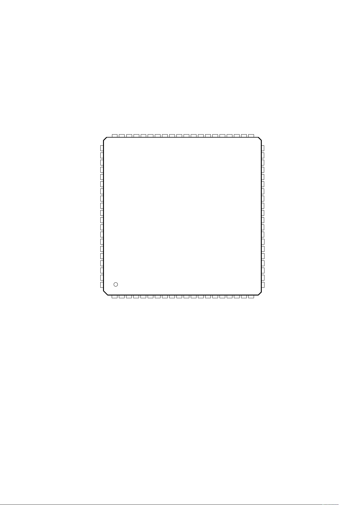
Figure 2–1. THS8200 Pin Location Diagram

2–2
Table 2–1. Terminal Functions
TERMINAL
NAME NO.
TYPE
†
DESCRIPTION
ABPb 15 O Analog output of DAC2. See AGY.
ARPr 17 O Analog output of DAC3. See AGY.
AGY 13 O Analog output of DAC1. With the proper setting of FSADJ<n>, this output is capable of driving 1.3 V full
scale into a 37.5 Ω load
AVDD 11, 14, 18 PWR Analog power supply, nominal 3.3 V
AVSS 12, 16 PWR Analog ground
BCb[9:0] 21–30 I 10-bit video data input port. All 10 bits or the 8 MSB of this port can be connected to the video data source. In
30-bit mode, the B data of RGB, or the Cb data of YCbCr, should be connected to this port. In 10-bit input
mode, this port is unused. In 20-bit input mode, this port is used for CbCr input data.
CLKIN 3 I Main clock input. Video input data on the GY[9:0]/BCb[9:0]/RCr[9:0] ports should be synchronized to
CLKIN. Depending on the input data format, CLKIN is supplied to THS8200 at 1 or 2 the pixel clock
frequency.
COMP1 10 P Compensation pin for the internal reference amplifier. A 0.1 µF capacitor should be connected between
COMP1 and analog power supply AVDD.
COMP2 9 P Compensation pin for the internal reference amplifier. A 0.1 µF capacitor should be connected between
COMP2 and analog power supply AVDD.
D1CLKO 71 O Video ITU-R.BT656-compliant clock output. This clock output is off by default and should be activated via
an I2C register setting.
DO[9:5]
DO[4:0]
65–69
73–77
O ITU-R.BT656 compliant video data output port. Only available when ITU-R.BT656 input format is used. Can
be used to connect to external PAL/NTSC video encoder . This port is off by default and should be activated
via an I2C register setting.
DVDD 32, 59, 79 PWR Digital core power, nominal 1.8 V
DVSS 31, 58, 78 PWR Digital core ground
FID 47 I Field identification signal for interlaced video formats. In slave timing mode, this is an input from the video
data source. In master timing mode this signal is unused, as only progressive-scan VESA formats are
supported in master mode.
FSADJ1 7 P Full scale adjustment control 1. A resistor should be connected between FSADJ1 and analog ground
AGND to control the full-scale output current of the DAC output channels. Via the data_fsadj I2C
programming register, the user can select between two full-scale ranges, determined by FSADJ1 or
FSADJ2.
For 700-mV video output (1 Vpp including sync), the nominal value is 2.99 kΩ ; for 1.0-Vpp video output (1.3
Vpp including sync) output the nominal value is 2.08 kΩ.
FSADJ2 8 P Full scale adjustment control 2. See FSADJ1.
GND_DLL 2 PWR Ground of clock doubler. Should be connected to analog ground
GND_IO 20, 45, 72 PWR I/O ring ground
GY[9:0] 48–57 I 10-bit video data input port. All 10 bits or the 8 MSB of this port can be connected to the video data source.
The G data of RGB or the Y data of YCbCr should be connected to this port. Port used in 10-bit mode for
CbYCrY video input data; in 20-bit input mode for Y data.
HS_IN 43 I/O Horizontal source synchronization. In slave timing mode, this is an input from the video data source. In
master timing mode, this is an output to the video data source with programmable timing and polarity,
serving as a horizontal data qualification signal to the video source.
HS_OUT 61 O Horizontal sync output (to display). Irrespective of slave/master timing mode configuration, this is always an
output with timing generated by the DTG.
I2CA 5 I I2C device address LSB selection
N.C. 1, 80 I Manufacturing test input. Must be tied to GND for normal operation.
PBKG
(VSS)
6 PWR Substrate ground. Should be connected to analog ground
†
I = input, O = output, B = bidirectional, PWR = power or ground, P = passive
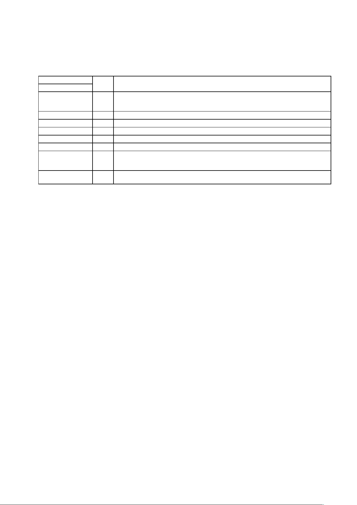
2–3
Table 2–1. Terminal Functions (Continued)
TERMINAL
NAME NO.
TYPE
†
DESCRIPTION
RCr[9:0] 33–42 I 10-bit video data input port. All 10-bits or the 8 MSB of this port can be connected to the video data source. In
30-bit mode, the R data of RGB or the Cr data of YCbCr should be connected to this port. In the 10- /20-bit
input mode, this port is unused. For some input formats this port is unused.
RESETB 60 I Software reset pin (active low). The minimum reset duration is 200 ns.
SCL 64 B Serial clock line of I2C bus interface. Open-collector. Maximum specified clock speed is 400 kHz (fast I2C).
SDA 63 B Serial data line of I2C bus interface. Open-collector
VDD_DLL 4 PWR Power supply of clock doubler, nominal 1.8 V
VDD_IO 19, 46, 70 PWR I/O ring power, 1.8 V or 3.3 V nominal
VS_IN 44 I/O V ertical source synchronization. In slave timing mode, this is an input from the video data source. In master
timing mode, this is an output to the video data source with programmable timing and polarity , serving as a
vertical data qualification signal to the video source.
VS_OUT 62 O Vertical sync output (to display). Irrespective of slave/master timing mode configuration, this is always an
output with timing generated by the DTG.
†
I = input, O = output, B = bidirectional, PWR = power or ground, P = passive
3–1
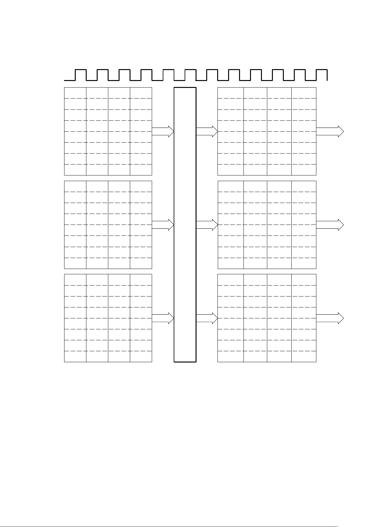
3 THS8200 Functional Overview
ifir
ifir
dly
eav
sav
scl_en
scl_out
scl_in
sda_en
sda_out
sda_in
rcr_in
bcb_in
gy_in
vs_in
hs_in
databus_in
databus_out
address
addr_en
ready
dg_bias
dr_bias
db_bias
digbypass
Three Channel DACs
4:2:2 to 4:4:4
Data Manager
I2C
Slave
arst_func_n
dig_mux
ifir12_bypass
ifir35_bypass
Color
Space
Convertor
ifir
ifir
ifir
Clip
Scale
Multiplier
Display
Timing
Generator
dig_mux
digbypass
Test Block
csmouts
ifirouts
dmanouts
dtg_data
dg_bias
vs_out
hs_out
dlclko
do[9:0]
dg
db_bias
db
dr_bias
dr
clk_fx2
clk_f
cdrv
clk_h
clkin
tstmode
2X
cgen
clkin
Clock Generator
Offset Binary Signals
cscouts
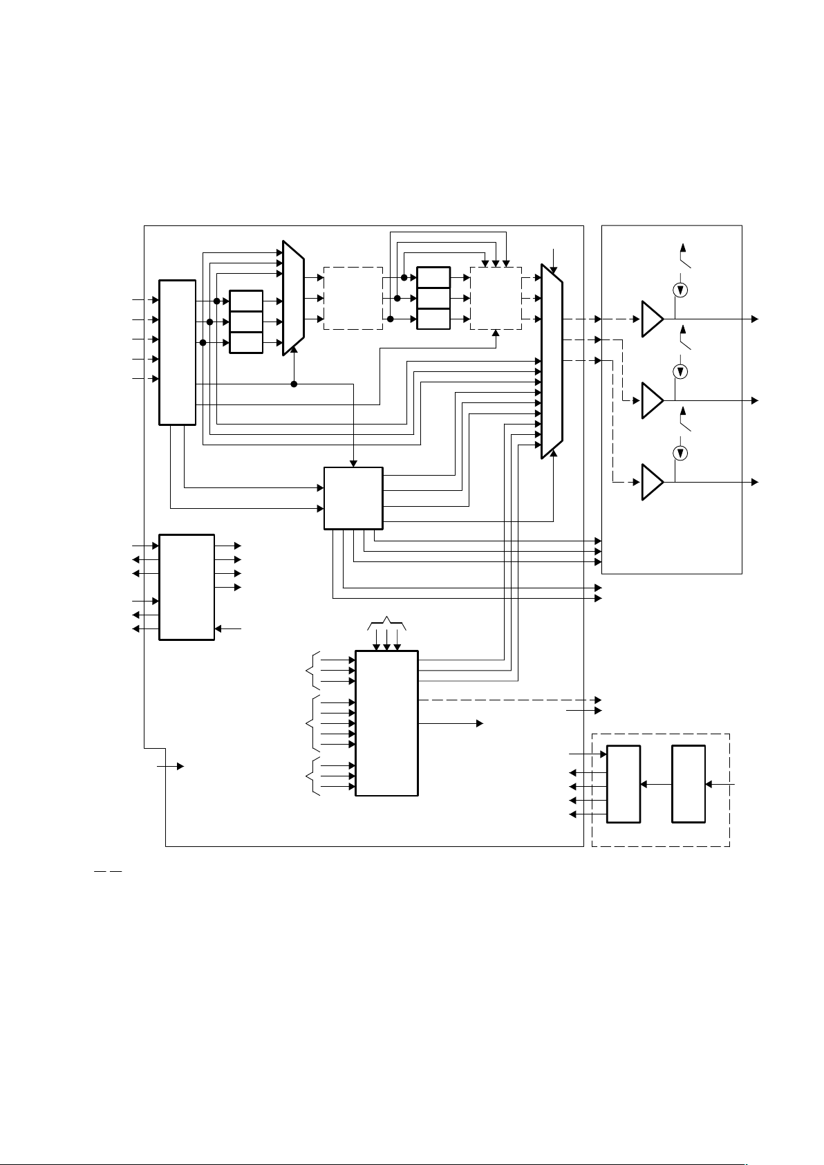
Figure 3–1. Functional Block Diagram
3.1 Data Manager (DMAN)
The data manager is the block that transforms the selected input video data format present on the chip input bus(es)
to an internal 10-bit three-channel representation. Supported input formats include 10/8 bit ITU-R.BT656 with
embedded sync codes, 15-/16- or 24-/30-bit RGB with external sync, 20-/16-bit SMPTE274M/296M with embedded
sync codes, as well as 20-/16-bit YCbCr 4:2:2 with external sync. The user can optionally include a 4:2:2 to 4:4:4

3–2
interpolation on the color data path. When a format with embedded sync is selected, DMAN also extracts H(Hsync),
V(Vsync), F(FieldID) identifiers from the ITU-R.BT656 (SDTV) or SMPTE274M/296M (HDTV) data stream for internal
synchronization of the DTG. Alternatively, the device synchronizes to HS_IN, VS_IN, FID inputs.
3.1.1 Interpolating Finite Impulse Responses Filter (IFIR)
The interpolating FIR is used to upsample the input data by 2× . In the THS82000 there are five IFIRs. The first two
are used only when the input data is in 4:2:2 format for conversion to a 4:4:4 internal representation on both color
difference channels. The last three IFIRs are used to upsample the internal data to the DACs on all three channels
in case 2× video interpolation is enabled. By 2× oversampling the video data, the requirements for the analog
reconstruction filter at the DAC outputs are relaxed so it can be built with fewer components, thereby also improving
the overall video frequency characteristic (less group delay variation). All of the IFIRs can be bypassed or switched
in by programming the appropriate I
2
C registers. The coefficients of all IFIRs are fixed.
3.1.2 Color-Space Conversion (CSC)
The color-space converter block is used to convert input video data in one type of color space to output video data
in another color space (e.g., RGB to YCbCr, or vice versa). This block contains a 3×3 matrix multiplier/adder and a
3×1 adder. All multiplier and adder coefficients can be programmed via the I
2
C interface to support any linear
matrixing+offset operation on the video data.
3.1.3 Clip/Shift/Multiplier (CSM)
The clip-shift-multiply block optionally clips the input code range at a programmed low/high code, shifts the input video
data downwards, and multiplies the input by a programmable coefficient in the range 0–1.999. This allows for
operation with a reduced input code range such as prescribed in the ITU-R.BT601 recommendation. Each channel
can be independently programmed to accommodate different digital ranges for each of the three input channels. For
example, for standard video signals the Y channel has a digital input range of 64–940, whereas the two other channels
have an input range of 64–960. All three channels must have a DAC output range of 0–700 mV , so normally the analog
voltage corresponding to 1 LSB would have to change to account for the different digital inputs. This might cause
matching errors. Therefore in the THS8200 the DAC LSB does not change; rather LSB conversion is done by scaling
the digital inputs to the DAC’s full input range. Furthermore, the CSM output is 11 bits wide and is sent to the 11-bit
DACs. The extra bit of resolution resolves nonlinearities introduced by the scaling process. The clipping function can
be switched off to allow for super-white/super-black excursions.
3.1.4 Digital Multiplexer (DIGMUX)
This multiplexer in front of the DACs can select between video signals at 1× or 2× the pixel clock rate. It is also used
to switch in blanking/sync level data generated by the display timing generator (DTG) block and test pattern data (e.g.,
color bars, I
2
C-controlled DAC levels) or to perform data insertion (CGMS) during vertical blanking.
3.1.5 Display Timing Generator (DTG)
The display timing generator is responsible for the generation of the correct frame format including all sync,
equalization and serration pulses. In master timing mode, the DTG is synchronized to external synchronization inputs,
either from the dedicated device terminals HS_IN, VS_IN, and FID or is synchronized to the identifiers extracted from
the input data stream, as selected by the DMAN mode. In master timing mode, the DTG generates the required
field/frame format based on the externally applied pixel clock input.
When active data is not being passed to the DACs, i.e., during the horizontal/vertical blanking intervals, the DTG
generates the correct digital words for blank, sync levels and other level excursions, such as pre- and post-serration
pulses and equalization pulses.
Horizontal timings, as well as amplitudes of negative and positive sync, HDTV broad pulses and SDTV pre- and
post-equalization and serration pulses, are all I
2
C-programmable to accommodate, e.g., the generation of both

3–3
EIA.770-1 (10:4 video/sync ratio) and EIA.770-2 (7:3 video/sync ratio) compliant analog component video outputs,
and to support nonstandard video timing formats.
In addition or as an alternative to the composite sync inserted on green/luma channel or all analog outputs, output
video timing can be carried via dedicated Hsync/Vsync output signals as well. The position, duration and polarity of
Hsync and Vsync outputs are fully programmable in order to support, for example, the centering of the active video
window within the picture frame.
The DTG also controls the data multiplexer in the DIGMUX block. DIGMUX can be programmed to pass device input
data only on active video lines (inserting DTG-generated blanking level during blanking intervals). Alternatively , the
DTG can pass device input data also during some VBI lines (ancillary data in the input stream is passed transparently
on some VBI lines). Finally , the device can also generate its own ancillary data and insert it into the analog outputs
according to the CGMS data format for the 525P video format.
3.1.6 Clock Generator (CGEN)
The clock generator is an analog delay-locked loop (DLL) based circuit and provides a 2× clock from the CLKIN input.
The 2× clock is used by the CDRV block for 2× video interpolation. Some video formats also require a 1/2 rate clock
used for 4:2:2 to 4:4:4 conversion.
3.1.7 Clock Driver (CDRV)
The clock drive block generates all on-chip clocks. Its inputs are control signals from the digital logic, the original
CLKIN, and the 2× clock from CGEN. Outputs include a half-rate clock, full-rate clock, and a 2× full-rate clock. The
clocks are used for both optional on-chip interpolation processes: 4:2:2 to 4:4:4 interpolation and 1× to 2× video
oversampling.
3.1.8 I2C Host Interface (I2CSLAVE)
The I2C interface controls and programs the internal I2C registers. The THS8200 I2C interface implementation
supports the fast I
2
C specification (SCL: 400 kHz) and allows the writing and reading of registers. An auto-increment
addressing feature simplifies block register programming. The I
2
C interface works without a clock present on CLKIN.
3.1.9 Test Block (TST)
The test block controls all the test functions of the THS8200. In addition to manufacturing test modes, this block
contains several user test modes including a DAC internal ramp generator and a 75% SMPTE video color bar
generator.
3.1.10 D/A Converters (DAC)
THS8200 contains three DACs operating at up to 205 MSPS and with an internal resolution of 11 bits. Each DAC
contains an integrated video sync inserter. The sync(s) is (are) inserted by means of additional current source circuits
either on the green/luma (Y) channel only or on all the DAC output channels, in order to be compliant with both
consumer (EIA, sync-on-G/Y) as well as professional (SMPTE, sync-on-all) standards.
The DAC speed supports all A TSC formats, including 1080P, as well as all PC graphics (VESA) formats up to UXGA
at 75 Hz (202.5 MSPS).
4–1
4 Detailed Functional Description
4.1 Data Manager (DMAN)
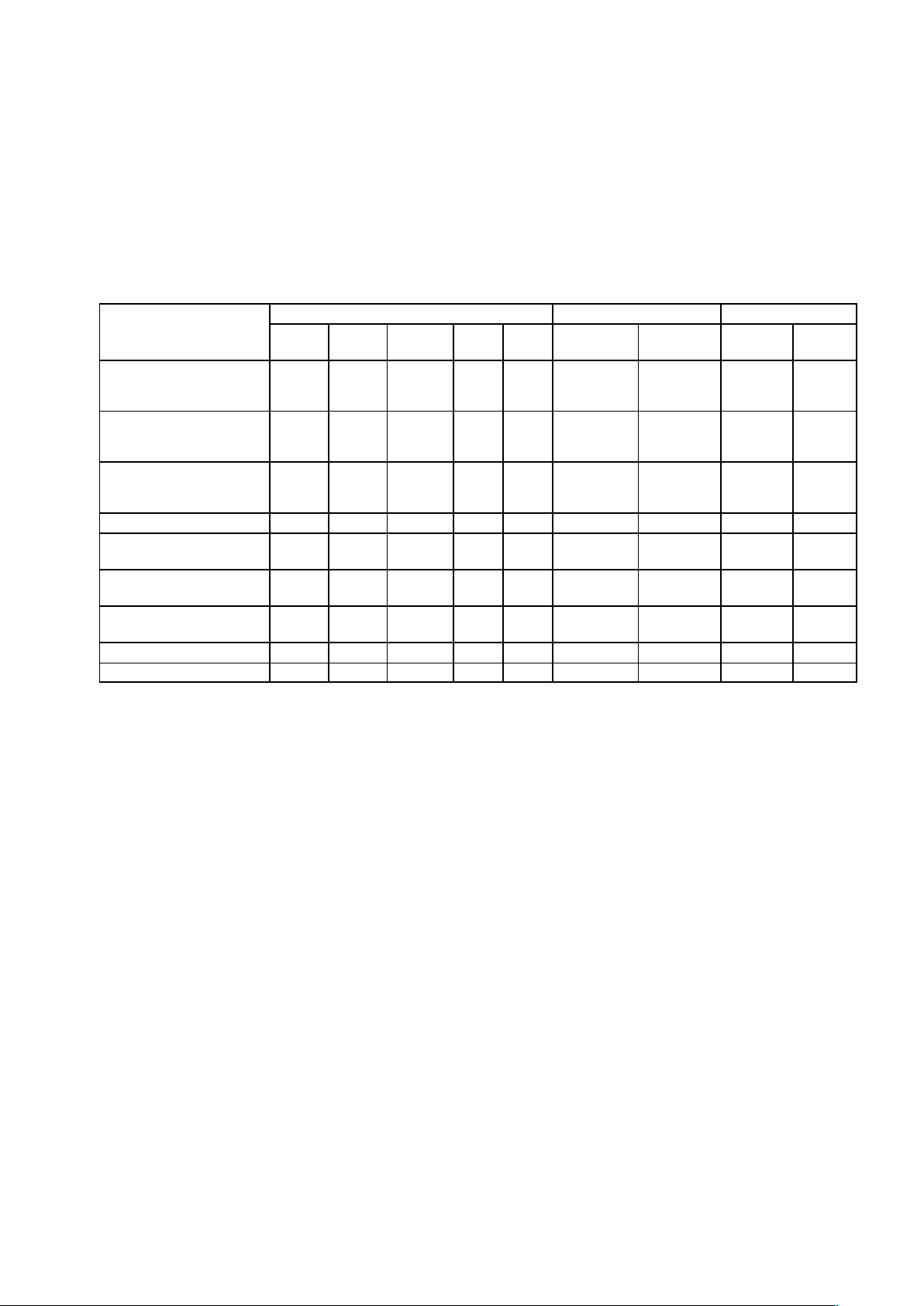
Table 4–1. Supported Input Formats
INPUT INTERFACE TIMING CONTROL SYNCHRONIZATION
30-BIT 20-BIT 10-BIT
(1)
16-BIT 15-BIT
EMBEDDED
TIMING
DEDICATED
TIMING
MASTER SLAVE
[PRESET]
HDTV-SMPTE296M
progressive (720P)
X (4:4:4) X (4:2:2) X X
[PRESET]
HDTV-SMPTE274M
progressive (1080P)
X (4:4:4) X (4:2:2) X X
[PRESET]
HDTV-SMPTE274M
progressive (1080I)
X (4:4:4) X (4:2:2) X X
[GENERIC] HDTV X (4:4:4) X (4:2:2) X X X
[PRESET]
SDTV-ITU.1358 (525P)
X
(2)
X X
[PRESET]
SDTV-ITU-R.BT470 (525I)
X
(3)
X X
[PRESET]
SDTV-ITU-R.BT470 (625I)
X
(3)
X X
[GENERIC] SDTV X (4:4:4) X (4:2:2) X X X
[PRESET] VESA X
(4)
X
(4)
X
(4)
X X X
NOTES: 1. When the device is configured to receive data over a 10-bit interface, the ITU-R.BT656 output bus on the THS8200 can be enabled
via an I2C register bit to send the received data to an external device.
In other DMAN modes, this output should remain off (data_tristate656 register).
2. SMPTE293M-compliant
3. ITU-R.BT656-compliant
4. Because PC graphics data is normally only 8 bits wide, only 3×8 bits (8 MSBs of each bus) are used. Color space converter bypass
is required for modes with pixel clock > 150 MSPS.
Table 4–1 summarizes all supported video mode configurations.
Each video mode is characterized by three attributes:
• Input Interface: Data is accepted over 10-, 20- or 30-bit interface (or 8 ,16, 24 bit interface for 8-bit data
when using 8 MSBs of each input data bus and connecting 2 LSBs to ground). This selection is controlled
by the dman_cntl register.
• Timing control: Video timing is either embedded in the data stream or supplied via dedicated timing
signals. In the latter case additional Hsync (HS_IN), Vsync (VS_IN) and FieldID (FID) input signals are
required to synchronize the video data source and THS8200 in the case of slave timing mode. This selection
is controlled by the dtg2_embedded_timing register.
• Synchronization: Video timing either is supplied to the device (slave) or the THS8200 requests video data
from the source (master). This selection is controlled by the chip_ms register.
NOTE: Device operation with combinations of settings for the dman_cntl,
dtg2_embedded_timing and chip_ms registers that result in operating modes not marked in
Table 4–1 is not assured. See detailed register map description for actual register settings.
Furthermore, Table 4–1 shows for which modes presets are defined. When in a preset video mode, the
line-type/breakpoint-pairs that define the frame format (see Display Timing Generator, Section 4.7) are
4–2
preprogrammed. Therefore the user does not need to define the table with line type/breakpoint settings, nor does
the field and frame size need to be programmed. However, when in preset mode, the horizontal parameters (all
dtg1_spec_x registers for the line types used by the preset setting, and dtg1_total_pixels registers) still need to be
programmed. Presets are available for most popular DTV video formats. Alternatively, generic modes for SDTV,
HDTV or VESA can be selected, which allow full programmability of the field/frame sizes and DTG parameters.
Note from the table that:
• If embedded timing is used, the device is always in slave mode, because the data stream supplied to
THS8200 contains the video timing information.
• Master operation is only supported for PC graphics (VESA) formats.
• In HDTV modes with embedded timing, data is supplied to the device over a 20-bit interface, as defined in
SMPTE274/296M.
• In SDTV modes with embedded timing, data is supplied to the device over a 10-bit interface. When the video
format is interlaced, this interface is known as ITU-R.BT656 (525I, 625I). When the video format is
progressive, only 525P is supported with embedded timing. The 625P interface can be supported with
dedicated timing, using the SDTV generic mode.
• In generic modes with dedicated timing, both 20 bits (4:2:2) and 30 bits (4:4:4) are supported.
• In PC graphics modes (VESA generic), input data is either over the 30-bit interface or over the 16-/15-bit
interface and always has dedicated timing. Note that the 16-bit interface is not equivalent to a 2×8-bit version
of the 20-bit interface; see Section 4.2, Input Interface Formats, for details.
4.2 Input Interface Formats
The following figures define the input video format for each input mode, as selected by the data_dman_cntl register
setting. Video data is always clocked in at the rising edge of CLKIN. Note: for 8-bit operation with 10-bit input buses,
connect only the 8 MSBs of each input bus used, and tie the 2 LSBs to ground.
• 30-bit YCbCr/RGB 4:4:4
G0/Y0
GY[9:0]/[9:2]
CLKIN
G1/Y1 G2/Y2 G3/Y3 G4/Y4 G5/Y5 G6/Y6 G7/Y7
B0/Cb0
BCb[9:0]/[9:2]
B1/Cb1 B2/Cb2 B3/Cb3 B4/Cb4 B5/Cb5 B6/Cb6 B7/Cb7
R0/Cr0
RCr[9:0]/[9:2]
R1/Cr1 R2/Cr2 R3/Cr3 R4/Cr4 R5/Cr5 R6/Cr6 R7/Cr7
Figure 4–1. 24-/30-Bit RGB or YCbCr Data Format
• 20-bit YCbCr 4:2:2
CLKIN is equal to the 1× pixel clock. The pixel clock equals the rate of the Y input and is 2× the rate of the 2 other
channels in this input format where Cb and Cr are multiplexed onto the same input bus.
4–3
Y7(0)
Y6(0)
Y5(0)
Y4(0)
Y3(0)
Y2(0)
Y1(0)
Y1(0)
Y7(1)
Y6(1)
Y5(1)
Y4(1)
Y3(1)
Y2(1)
Y1(1)
Y1(1)
Y7(2)
Y6(2)
Y5(2)
Y4(2)
Y3(2)
Y2(2)
Y1(2)
Y1(2)
Y7(3)
Y6(3)
Y5(3)
Y4(3)
Y3(3)
Y2(3)
Y1(3)
Y1(3)
GY[9]
GY[8]
GY[7]
GY[6]
GY[5]
GY[4]
GY[3]
GY[2]
Cb7(0)
Cb6(0)
Cb5(0)
Cb4(0)
Cb3(0)
Cb2(0)
Cb1(0)
Cb0(0)
Cr7(0)
Cr6(0)
Cr5(0)
Cr4(0)
Cr3(0)
Cr2(0)
Cr1(0)
Cr0(0)
Cb7(2)
Cb6(2)
Cb5(2)
Cb4(2)
Cb3(2)
Cb2(2)
Cb1(2)
Cb0(2)
Cr7(2)
Cr6(2)
Cr5(2)
Cr4(2)
Cr3(2)
Cr2(2)
Cr1(2)
Cr0(2)
BCb[9]
BCb[8]
BCb[7]
BCb[6]
BCb[5]
BCb[4]
BCb[3]
BCb[2]
X
X
X
X
X
X
X
X
X
X
X
X
X
X
X
X
X
X
X
X
X
X
X
X
X
X
X
X
X
X
X
X
RCr[9]
RCr[8]
RCr[7]
RCr[6]
RCr[5]
RCr[4]
RCr[3]
RCr[2]
CLKIN
Data Manager
Cb7(0)
Cb6(0)
Cb5(0)
Cb4(0)
Cb3(0)
Cb7(2)
Cb6(2)
Cb5(2)
Cb4(2)
Cb3(2)
TO CH1
TO CH2
TO CH3
Y7(0)
Y6(0)
Y5(0)
Y4(0)
Y3(0)
Y2(0)
Y1(0)
Y1(0)
Y6(1)
Y7(2)
Y6(2)
Y5(2)
Y4(2)
Y3(2)
Y2(2)
Y1(2)
Y1(2)
Y7(3)
Y6(3)
Y5(3)
Y4(3)
Y3(3)
Y2(3)
Y1(3)
Y1(3)
Cb2(0)
Cb1(0)
Cb0(0)
Cb2(2)
Cb1(2)
Cb0(2)
Cr7’(1) Cr7(2)
Cr6(2)
Cr5(2)
Cr4(2)
Cr3(2)
Cr6’(1)
Cr5’(1)
Cr4’(1)
Cr3’(1)
Cr2’(1)
Cr1’(0)
Cr0’(1)
Cr2(2)
Cr1(2)
Cr0(2)
Cr7(0)
Cr6(0)
Cr5(0)
Cr4(0)
Cr3(0)
Cr2(0)
Cr1(0)
Cr0(0)
Cr7’(3)
Cr6’(3)
Cr5’(3)
Cr4’(3)
Cr3’(3)
Cr2’(3)
Cr1’(3)
Cr0’(3)
Y7(1)
Y5(1)
Y4(1)
Y3(1)
Y2(1)
Y1(1)
Y1(1)
Cb7’(1)
Cb5’(1)
Cb4’(1)
Cb3’(1)
Cb2’(1)
Cb1’(1)
Cb0’(1)
Cb6’(1)
Cb7’(3)
Cb6’(3)
Cb5’(3)
Cb4’(3)
Cb3’(3)
Cb2’(3)
Cb1’(3)
Cb0’(3)
NOTE: Where Cb’Cr’ are the output of half-band interpolation filter.
Figure 4–2. 20-/16-Bit YCbCr 4:2:2 Data Format (16-Bit Operation Shown)
When dedicated timing is used in this mode, there is a fixed relationship between the first active period of HS_IN (i.e.,
the first CLKIN rising edge seeing HS_IN active) and a Cb color component assumed present during that clock period
on the bus receiving CbCr samples. When embedded timing is used in this mode, the SAV/EAV structure also
unambiguously defines the CbCr sequence, according to SMPTE274M/296M for HDTV.
NOTE: The figure shows the case when only 8 bits of each 10-bit input bus are used.
• 10-bit YCbCr 4:2:2 (ITU mode)
CLKIN is equal to 2× the pixel clock since all components are multiplexed on a single 10-bit bus with a 4-multiple
sequence: CbYCrY. Therefore the pixel clock (i.e., the Y input rate) is 1/2 of CLKIN and the Cb and Cr rate are 1/4
of CLKIN.
4–4
When dedicated timing is used in this mode, there is a fixed relationship between the first active period of HS_IN (i.e.
the first CLKIN rising edge seeing HS active) and a Cb color component assumed present during that clock period
on the input bus. When embedded timing is used in this mode, the SA V/EAV structure also unambiguously defines
the CbCr sequence, according to ITU-R.BT656 (for 625I and 525I) and SMPTE293M (for 525P).
• 16-bit RGB 4:4:4
R7(0)
R6(0)
R5(0)
R4(0)
R3(0)
G7(0)
G6(0)
G5(0)
R7(1)
R6(1)
R5(1)
R4(1)
R3(1)
G7(1)
G6(1)
G5(1)
R7(2)
R6(2)
R5(2)
R4(2)
R3(2)
G7(2)
G6(2)
G5(2)
R7(3)
R6(3)
R5(3)
R4(3)
R3(3)
G7(3)
G6(3)
G5(3)
GY[9]
GY[8]
GY[7]
GY[6]
GY[5]
GY[4]
GY[3]
GY[2]
G4(0)
G3(0)
G2(0)
B7(0)
B6(0)
B5(0)
B4(0)
B3(0)
G4(1)
G3(1)
G2(1)
B7(1)
B6(1)
B5(1)
B4(1)
B3(1)
G4(2)
G3(2)
G2(2)
B7(2)
B6(2)
B5(2)
B4(2)
B3(2)
G4(3)
G3(3)
G2(3)
B7(3)
B6(3)
B5(3)
B4(3)
B3(3)
BCb[9]
BCb[8]
BCb[7]
BCb[6]
BCb[5]
BCb[4]
BCb[3]
BCb[2]
X
X
X
X
X
X
X
X
X
X
X
X
X
X
X
X
X
X
X
X
X
X
X
X
X
X
X
X
X
X
X
X
RCr[9]
RCr[8]
RCr[7]
RCr[6]
RCr[5]
RCr[4]
RCr[3]
RCr[2]
CLKIN
Data Manager
G7(0)
G6(0)
G5(0)
G4(0)
G3(0)
G2(0)
0
0
G7(1)
G6(1)
G5(1)
G4(1)
G3(1)
G2(1)
0
0
G7(2)
G6(2)
G5(2)
G4(2)
G3(2)
G2(2)
0
0
G7(3)
G6(3)
G5(3)
G4(3)
G3(3)
G2(3)
0
0
B7(0)
B6(0)
B5(0)
B4(0)
B3(0)
0
0
0
B7(1)
B6(1)
B5(1)
B4(1)
B3(1)
0
0
0
B7(2)
B6(2)
B5(2)
B4(2)
B3(2)
0
0
0
B7(3)
B6(3)
B5(3)
B4(3)
B3(3)
0
0
0
R7(0)
R6(0)
R5(0)
R4(0)
R3(0)
0
0
0
R7(1)
R6(1)
R5(1)
R4(1)
R3(1)
0
0
0
R7(2)
R6(2)
R5(2)
R4(2)
R3(2)
0
0
0
R7(3)
R6(3)
R5(3)
R4(3)
R3(3)
0
0
0
TO CH1
TO CH2
TO CH3
Figure 4–3. 16-Bit RGB 4:4:4 Data Format
CLKIN is equal to 1× the pixel clock. This format is only supported in VESA mode and can be used for PC graphics
applications that do not require full 8-bit resolution on each color component.
4–5
• 15-bit RGB 4:4:4
R7(0)
R6(0)
R5(0)
R4(0)
R3(0)
G7(0)
G6(0)
G5(0)
R7(1)
R6(1)
R5(1)
R4(1)
R3(1)
G7(1)
G6(1)
G5(1)
R7(2)
R6(2)
R5(2)
R4(2)
R3(2)
G7(2)
G6(2)
G5(2)
R7(3)
R6(3)
R5(3)
R4(3)
R3(3)
G7(3)
G6(3)
G5(3)
GY[9]
GY[8]
GY[7]
GY[6]
GY[5]
GY[4]
GY[3]
GY[2]
G4(0)
G3(0)
B7(0)
B6(0)
B5(0)
B4(0)
B3(0)
G4(1)
G3(1)
B7(1)
B6(1)
B5(1)
B4(1)
B3(1)
G4(2)
G3(2)
B7(2)
B6(2)
B5(2)
B4(2)
B3(2)
G4(3)
G3(3)
B7(3)
B6(3)
B5(3)
B4(3)
B3(3)
BCb[9]
BCb[8]
BCb[7]
BCb[6]
BCb[5]
BCb[4]
BCb[3]
BCb[2]
X
X
X
X
X
X
X
X
X
X
X
X
X
X
X
X
X
X
X
X
X
X
X
X
X
X
X
X
X
X
X
X
RCr[9]
RCr[8]
RCr[7]
RCr[6]
RCr[5]
RCr[4]
RCr[3]
RCr[2]
CLKIN
Data Manager
G7(0)
G6(0)
G5(0)
G4(0)
G3(0)
0
0
0
G7(1)
G6(1)
G5(1)
G4(1)
G3(1)
0
0
0
G7(2)
G6(2)
G5(2)
G4(2)
G3(2)
0
0
0
G7(3)
G6(3)
G5(3)
G4(3)
G3(3)
0
0
0
B7(0)
B6(0)
B5(0)
B4(0)
B3(0)
0
0
0
B7(1)
B6(1)
B5(1)
B4(1)
B3(1)
0
0
0
B7(2)
B6(2)
B5(2)
B4(2)
B3(2)
0
0
0
B7(3)
B6(3)
B5(3)
B4(3)
B3(3)
0
0
0
R7(0)
R6(0)
R5(0)
R4(0)
R3(0)
0
0
0
R7(1)
R6(1)
R5(1)
R4(1)
R3(1)
0
0
0
R7(2)
R6(2)
R5(2)
R4(2)
R3(2)
0
0
0
R7(3)
R6(3)
R5(3)
R4(3)
R3(3)
0
0
0
TO CH1
TO CH2
TO CH3
XXXX
Figure 4–4. 15-Bit RGB 4:4:4 Data Format
CLKIN is equal to 1× the pixel clock. This format is only supported in VESA mode and can be used for PC graphics
applications that do not require full 8-bit resolution on each color component.
4.3 Clock Generator (CGEN)/Clock Driver (CDRV)
The clock generator/clock driver blocks generate all on-chip clocks for 4:2:2 to 4:4:4 and 2× video oversampling. The
DMAN setting controls whether the input data is 4:2:2 or 4:4:4 sampled, and whether a 30-, 20- or 10-bit interface
is used. This selection affects the clock input frequency assumed to be present on CLKIN.

4–6
• 30-bit 4:4:4: 1× pixel clock. 4:2:2 to 4:4:4 interpolation should be bypassed. Optional 2× oversampling is
available for formats with pixel clock up to 80 MHz.
• 20-bit 4:2:2: 1× pixel clock. 4:2:2 to 4:4:4 interpolation should be switched in, and is available for formats
with pixel clock up to 150 MHz. Optional 2× oversampling available for formats with pixel clock up to 80 MHz.
• 10-bit 4:2:2 (ITU): 1/2× pixel clock. 4:2:2 to 4:4:4 interpolation should be switched in, and is available for
formats with pixel clock up to 150 MHz. Optional 2× oversampling is available for formats with pixel clock
up to 80 MHz.
The internal DLL (delay-locked loop) generates the higher clock frequencies. The user should program the input
frequency range selection register, dll_freq_sel, according to the frequency present on CLK_IN when using either
or both interpolation/oversampling stages.
The 4:2:2 to 4:4:4 stage is switched in or bypassed, depending on the setting of data_ifir12_bypass register
(interpolation only on chroma channels). This feature should only be used with YCbCr 4:2:2 input. The THS8200 can
perform color space conversion to RGB depending on the CSC setting. The dtg2_rgbmode_on register should be
set corresponding to the color space representation of the DAC output.
The 2× oversampling stage is switched in or bypassed, depending on the setting of data_ifir35_bypass register.
The user should not enable the 2× oversampling stage when the CLK_IN frequency exceeds 80 MHz, as is the case
for the higher PC graphics formats and 1080P HDTV. In this case the DLL should be bypassed using the vesa_clk
register to disable the 2× frequency generation. As explained in the detailed register map description for this register,
it is still possible to support 20-bit 4:2:2 input in this mode (e.g., for 1080P).
A second bypass mode operation exists for the DLL, enabled by the dll_bypass register. When this bypass mode is
active, the CLKIN input is assumed to be 2× pixel frequency. This mode is meant only for test purposes as it does
not correspond to any mode in the supported input formats table.
4.4 Color Space Conversion (CSC)
THS8200 contains a fully-programmable 3×3 multiply/add and 3×1 adder block that can be switched in for all video
formats up to a pixel clock frequency of 150 MHz. Color space conversion is thus available for all DTV modes,
including 1080P and VESA modes up to SXGA at 75 Hz (135 MSPS). The operation is done after optional 4:2:2 to
4:4:4 conversion, and thus on the 1× pixel clock video data prior to optional 2× video oversampling. The CSC block
can be switched in or bypassed depending on the setting of register csc_bypass.
Each of the nine floating point multiplier coefficients of the 3×3 multiply/add is represented as the combination of a
6-bit signed binary integer part, and a 10-bit fractional part. The integer part is a signed magnitude representation
with the MSB as the sign bit. The fractional part is a magnitude representation; see the following example.
The register nomenclature is: csc_<r,g,b> <i,f>c<1,2,3> where:
• <r,g,b> identifies which input channel is multiplied by this coefficient (r = red/Cr, g = green/Y, b = blue/Cb
input)
• <i,f> identifies the integer (i) or fractional (f) part of the coefficient
• <1,2,3> identifies the output channel from the color space converter: 1 = Yd/Gd, 2 = Cb/Bd, 3 = Cr/Rd
For the offset values, a value of 1/4 of the desired digital offset needs to be programmed in the individual offset register ,
so a typical offset of 512 (offset over 1/2 of the video range) requires programming a value of 128 decimal into the
offset<1,2,3> registers, where again <1,2,3> defines the output channel affected, with similar convention as shown
previously.
Saturation logic can be switched in to avoid over- and underflow on the result after color space conversion using the
csc_uof_cntl register.
We next show an example of how to program the CSC. This also explains the numeric data formats.
CSC configuration example: HDTV RGB to HDTV YCbCr
4–7
The formulas for RGB to YCbCr conversion are:
• Yd = 0.2126*Rd + 0.7152*Gd + 0.0722*Bd
• Cb = –0.1172*Rd – 0.3942*Gd + 0.5114*Bd + 512
• Cr = 0.5114*Rd – 0.4646*Gd – 0.0468*Bd + 512
To program the red coefficient of channel 1 (Y) with the value of 0.2126 the following must be done:
1. Realize that this is a positive value so the sign bit of the integer part is 0. (bit 5 of csc_ric1 = 0)
2. Note that there is no integer portion of the coefficient (bit 4–bit 0 = 00000).
3. The binary representation of the fractional part can be constructed directly from the binary equivalent of the
fractional part multiplied by 1024 (0.2126 × 1024 = 217.7), rounded to the nearest integer (218) and
represented as a binary 10-bit number (00 1101 1010).
Using the above method all the registers for the CSC blocks can be programmed with the correct value for RGB to
YCbCr conversion. Below is a complete list of register values for the above conversion.
0.2126 –> csc_ric1 = 00 0000 csc_rfc1 = 00 1101 1010
0.7152 –> csc_gic1 = 00 0000 csc_gfc1 = 10 1101 1100
0.0722 –> csc_bic1 = 00 0000 csc_bfc1 = 00 0100 1010
–0.1172 –> csc_ric2 = 10 0000 csc_rfc2 = 00 0111 1000
–0.3942 –> csc_gic2 = 10 0000 csc_gfc2 = 01 1001 0100
0.5114 –> csc_bic2 = 00 0000 csc_bfc2 = 10 0000 1100
0.5114 –> csc_ric3 = 00 0000 csc_rfc3 = 10 0000 1100
–0.4646 –> csc_gic3 = 10 0000 csc_gfc3 = 01 1101 1100
–0.0468 –> csc_bic3 = 10 0000 csc_bfc3 = 00 0011 0000
For the offsets necessary in the second and third equation the csc_offset<n> registers need to be programmed. We
need to add 512 to the Cb and Cr channels. The value to be programmed is 1/4 of this offset in a signed magnitude
representation, thus 128 or csc_offset2 = csc_offset3 = 00 1000 0000.
Packing these individual registers into the I
2
C register map, the programmed values are:
SUBADDRESS REGISTER NAME VALUE SUBADDRESS REGISTER NAME VALUE
0x04 csc_r11 0000 0000
0x0F csc_g32 1101 1100
0x05 csc_r12 1101 1010 0x10 csc_b11 0000 0000
0x06 csc_r21 1000 0000 0x11 csc_b12 0100 1010
0x07 csc_r22 0111 1000 0x12 csc_b21 0000 0010
0x08 csc_r31 0000 0010 0x13 csc_b22 0000 1100
0x09 csc_r32 0000 1100 0x14 csc_b31 1000 0000
0x0A csc_g11 0000 0010 0x15 csc_b32 0011 0000
0x0B csc_g12 1101 1100 0x16 csc_offs1 0000 0000
0x0C csc_g21 1000 0001 0x17 csc_offs12 0000 1000
0x0D csc_g22 1001 0100 0x18 csc_offs23 0000 0010
0x0E csc_g31 1000 0001 0x19 csc_offs3 0000 0000
CSC configuration example: HDTV YCbCr to HDTV RGB
• Gd = –0.4577*Cr + Yd – 0.1831*Cb +328 (= 0.6408*128*4)
• Bd = 0*Cr + Yd + 1.8142* Cb – 929 (= –1.8142*128*4)
• Rd = 1.5396* Cr +Yd +0*Cb – 788 (= –1.5396*128*4)
4–8
In a similar manner, it can be calculated that the programming array is in this case:
SUBADDRESS REGISTER NAME VALUE SUBADDRESS REGISTER NAME VALUE
0x04 csc_r11 1000 0001
0x0F csc_g32 0000 0000
0x05 csc_r12 1101 0101 0x10 csc_b11 1000 0000
0x06 csc_r21 0000 0000 0x11 csc_b12 10111011
0x07 csc_r22 0000 0000 0x12 csc_b21 0000 0111
0x08 csc_r31 0000 0110 0x13 csc_b22 0100 0010
0x09 csc_r32 0010 1001 0x14 csc_b31 0000 0000
0x0A csc_g11 0000 0100 0x15 csc_b32 0000 0000
0x0B csc_g12 0000 0000 0x16 csc_offs1 0001 0100
0x0C csc_g21 0000 0100 0x17 csc_offs12 1010 1110
0x0D csc_g22 1000 0000 0x18 csc_offs23 1000 1011
0x0E csc_g31 0000 0100 0x19 csc_offs3 0001 0100
4.5 Clip/Scale/Multiplier (CSM)
There are limits on the code range of the video data if sampled according to ITU or SMPTE standards. In other words,
the full 10-bit range [0:1023] is not used to represent video pixels. For example, typically 64 decimal is the lowest code
allowed to represent a video signal and corresponds to the blanking level. Similarly for Y, typically the maximum code
is 940 decimal. Excursions outside this range can be the result of digital video processing.
THS8200 can handle such instantaneous excursions in either of two ways: by limiting the input codes to
programmable max/min values, or by allowing such excursions to occur.
Depending on which approach is chosen, the user can scale up the video data in the CSM to make sure the full-scale
dynamic range of the DAC is used for optimal performance when using limiting. Alternatively, the instantaneous
excursions outside the code range can be output by the DAC in the analog output signal (allowing super-white/black
in analog output) when this clipping is disabled.
The CSM block allows the user to specify the behavior of THS8200 with such reduced-swing input video codes. It
consists of the following:
1. an optional clipping of the input video data at a high and low limit, where the limits are individually
programmable per channel
2. a downward shift of the input video data, where the shift amount is individually programmable per channel
3. a multiply (magnitude scaling) function of the video data, where the multiplier coefficient is individually
programmable per channel.
4.5.1 Clipping
Clipping (limiting) of the video input data can be turned on or off on a per-channel basis, and selectively at the high
and/or low end, by programming the csm_<gy ,rcr,bcb>_<high,low>_clip_on registers. The high/low clipping values
can be programmed on a per-channel basis using registers csm_clip_<gy,rcr,bcb>_<high,low>.
Figure 4–5 shows a typical situation to clip ITU-R.BT601 sampled video signals.
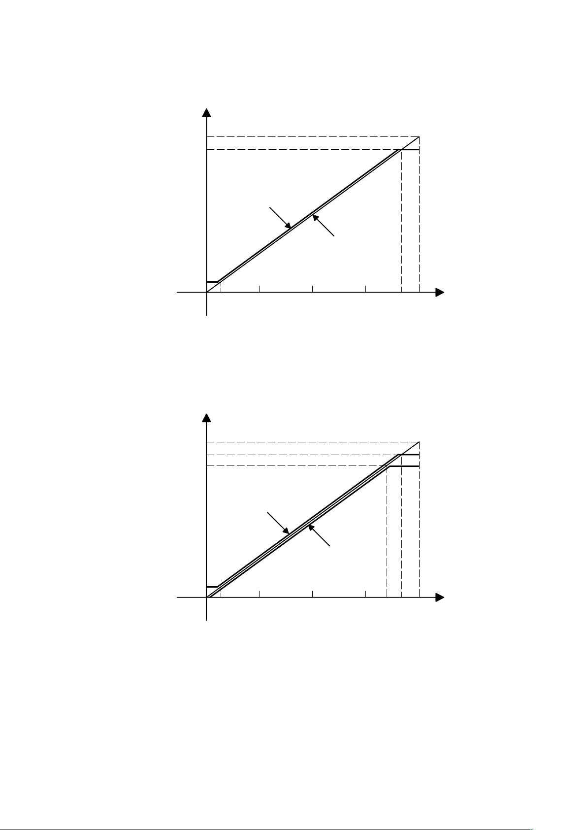
4–9
1023
940
817.3 mV
751.1 mV
51.1 mV
255 767511
64
0
Input Digital Codes
Analog Output From DACs
Ramping Analog Output With Clipping Effect on Top and Bottom
Output After
Clipping
Output Before
Clipping
Figure 4–5. Effect of Clipping on Analog Output
4.5.2 Shifting
Next the video data can be shifted over a programmable amount downward. The number of codes over which to shift
the input video data is set per channel by programming csm_shift_<gy ,rcr ,bcb>. Shifting of the input video data can
be done downwards over 0..255 codes inside the CSM.
1023
940
817.3 mV
751.1 mV
51.1 mV
255 767511
64
0
Input Digital Codes
Analog Output From DACs
Ramping Analog Output With Clipping Effect on Top and Bottom
700.0 mV
876
Output After
Clipping and
Shifting
Output After
Clipping
Figure 4–6. Effect of Shifting on Clipped Analog Output
4–10
Figure 4–5 and Figure 4–6 also show the analog output from the DAC if the full-scale video range over the [64..940]
input would correspond to the normal 700 mV range for component video. This full-scale range is set by the selected
FSADJ full-scale setting (register data_fsadj).
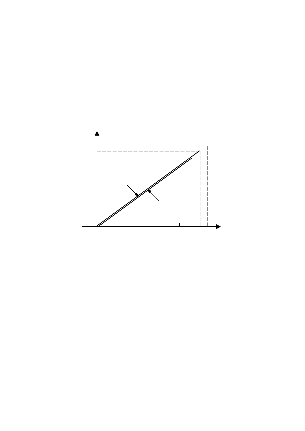
4.5.3 Multiplying
When the 10-bit range is not fully used for video, we can scale the input video data to use the full 10-bit dynamic range
of the DACs. Care should be taken not to over/underflow the available range after scaling.
This multiplying control serves two purposes:
• Use of the full 10-bit DAC range for inputs of reduced range
• Individual fine gain control per channel to compensate for gain errors and provide white balance control
1023
964
817.3 mV
770.0 mV
255 767511
0
Input Digital Codes
Analog Output From DACs
Ramping Analog Output With 1:1.1 AC Range Fine Scaling
Range After
Scaling Up 1:1.1
700.0 mV
876
DC Shifted
Original AC Range
Figure 4–7. Effect of Scaling the Analog Video Output
Figure 4–7 illustrates a shifted analog ramping output. The multiplication factor could be calculated to scale this
output range to the full 10-bit range of the DAC. Note that this scaling can be programmed individually per channel
using registers csm_mult_<gy ,rcr,bcb>. The range of the multiplication is 0..1.999, coded as a binary weighted 1 1-bit
value, thus: csm_mult_<gy,rcr,bcb> = (Desired scale ( 0 to 1.999) / 1.999) × 2047
Note that this approach allows to scale input code ranges that are different on each channel to an identical full-scale
DAC output compliance, as is required for ITU-R.BT601 sampled signals where Y video data is represented in the
range [64..940] and both Cb,Cr color difference channels are coded within the range [64..960]. All three channels
need to generate a 700-mV nominal analog output compliance. Using a combination of FSADJ—adjusting the
full-scale current of all DAC channels simultaneously in the analog domain—and digital CSM control, different
trade-offs can be made for DAC output amplitude control, including channel matching.
As discussed in Display Timing Generator (Section 4.7), the user also controls the DAC output levels during blanking,
negative and positive sync, pre- and post-equalization, and serration pulses. Using a combination of CSM and DTG
programming, it is therefore possible to accommodate many video standards, including those that require a video
blank-to-black level setup, as well as differing video/sync ratios (e.g., 10:4 or 7:3).
Finally, using the selectable full-scale adjustment from the FSADJ1 or FSADJ2 terminals, it is possible to switch
between two analog output compliance settings with no hardware changes.
Physically , the CSM output is represented internally as an 1 1-bit value to improve the DAC linearity at the 10-bit level
after scaling. Each DAC internally is of 11-bit resolution.
4–11
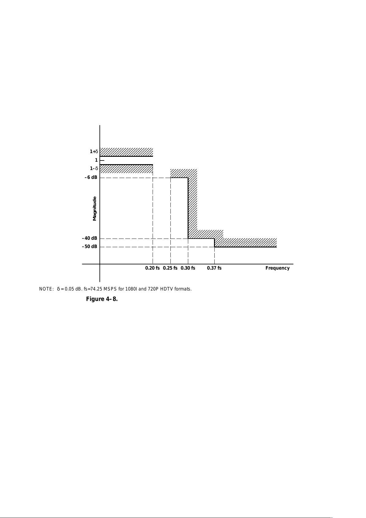
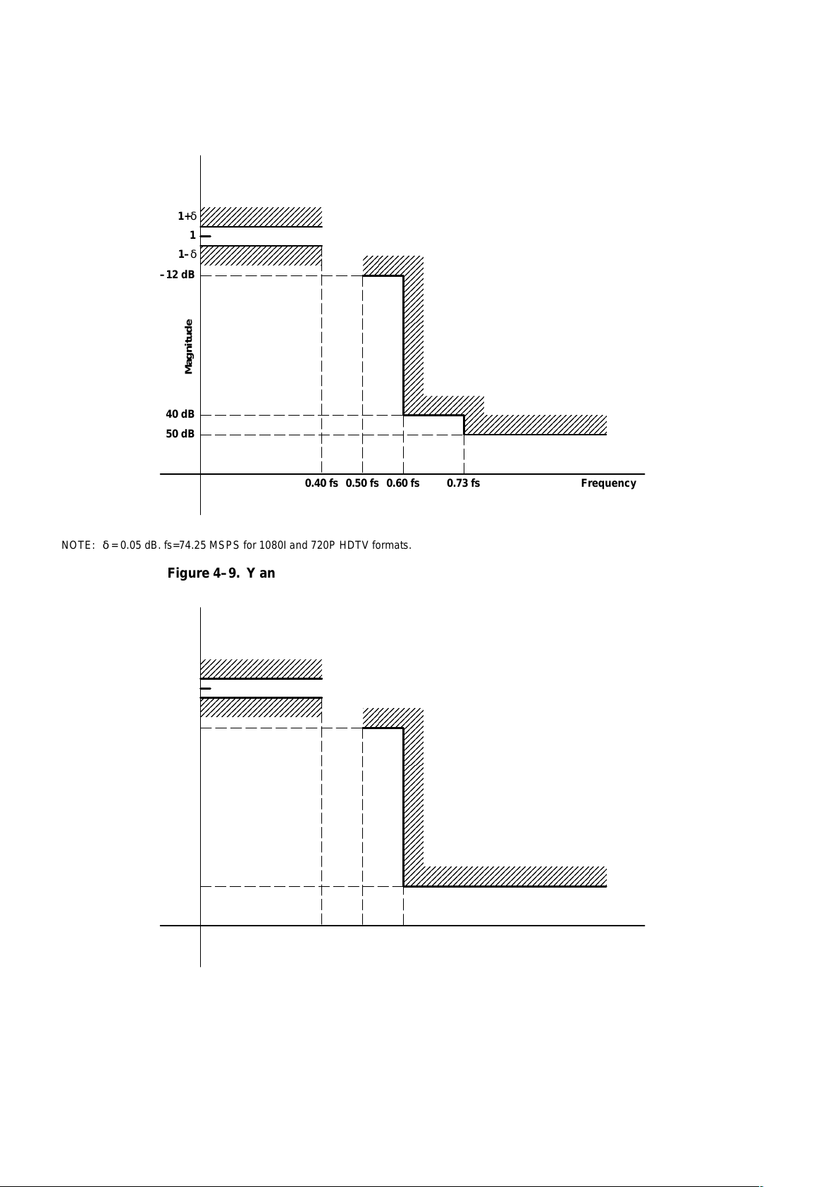
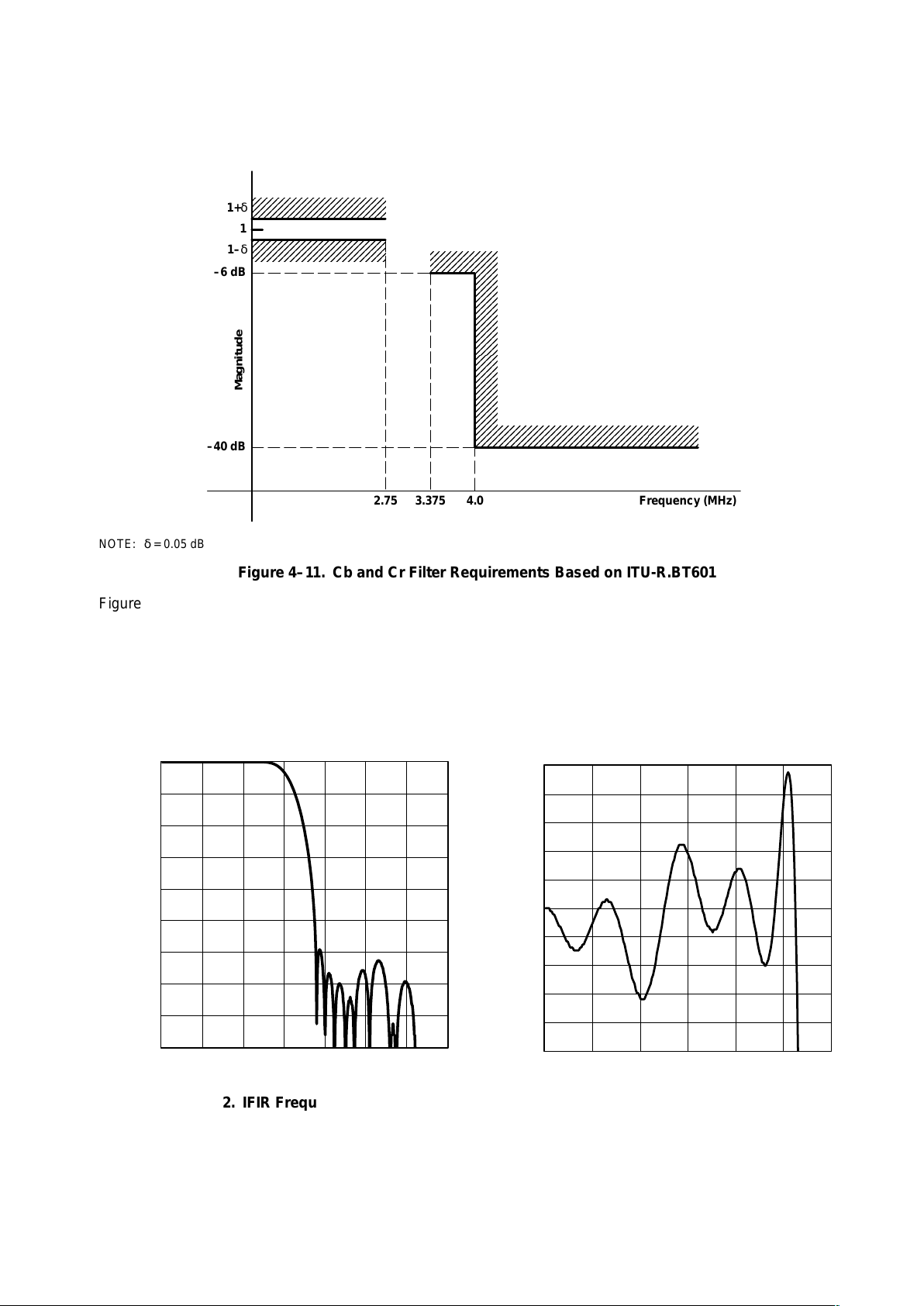
4.6 Interpolating Finite Impulse Response Filter (IFIR)
For relaxing the requirements of the reconstruction filter behind the DAC in the analog domain, and in order to take
advantage of the high-speed capability of the DACs in THS8200, a 2× digital up-sampling and interpolation filter
module is integrated.
Figure 4–8 through Figure 4–11 show the YRGB and CbCr filtering requirements for HDTV (SMPTE274M/296M
standards) and SDTV (ITU-R.BT601 standard), respectively.
0.20 fs
1+δ
Frequency
1
0.25 fs
1–δ
–6 dB
–40 dB
–50 dB
0.30 fs 0.37 fs
Magnitude
NOTE: δ = 0.05 dB. fs=74.25 MSPS for 1080I and 720P HDTV formats.
Figure 4–8. PB and PR Filter Requirements Based on SMPTE 296M/274M
4–12
0.40 fs
1+δ
Frequency
1
0.50 fs
1–δ
–12 dB
40 dB
50 dB
0.60 fs 0.73 fs
Magnitude
NOTE: δ = 0.05 dB. fs=74.25 MSPS for 1080I and 720P HDTV formats.
Figure 4–9. Y and RGB Filter Requirements Based on SMPTE 296M/274M
5.75
1+δ
Frequency (MHz)
1
6.75
1–δ
–12 dB
–40 dB
8.0
Magnitude
NOTE: δ = 0.05 dB.
Figure 4–10. Y and RGB Filter Requirements Based on ITU-R.BT601
4–13
2.75
1+δ
Frequency (MHz)
1
3.375
1–δ
–6 dB
–40 dB
4.0
Magnitude
NOTE: δ = 0.05 dB
Figure 4–11. Cb and Cr Filter Requirements Based on ITU-R.BT601
Figure 4–12 through Figure 4–14 illustrate the frequency and phase responses of the interpolating filters. The actual
response using the finite-word length coefficients present in THS8200 is shown. The same filter characteristic is used
for SDTV/HDTV modes and for both 4:2:2 to 4:4:4 interpolation (2 filters, one on each of Cb and Cr channels, switched
in when a 4:2:2 input mode is selected on DMAN to interpolate chrominance from 1/2 to 1× pixel clock rate) as well
as for 2× video oversampling (3 filters, one on each DAC channel, switched in when 2× interpolation is activated).
f – Frequency – Rad
–90
–80
–70
–60
–50
–40
–30
–20
–10
0
0.0 0.5 1.0 1.5 2.0 2.5 3.0 3.5
Magnitude – dB
MAGNITUDE
vs
FREQUENCY
f – Frequency – Rad
0
1
2
3
4
5
6
7
8
9
10
0.00 0.25 0.50 0.75 1.00 1.25 1.50
Magnitude – dB
MAGNITUDE
vs
FREQUENCY
0.01
0.008
0.006
0.004
0.002
0
–0.002
–0.004
–0.006
–0.008
–0.01
Figure 4–12. IFIR Frequency Response
Figure 4–13. IFIR Pass-Band Frequency Response
4–14
f – Frequency – Rad
–4
–3
–2
–1
0
1
2
3
4
0.0 0.5 1.0 1.5 2.0 2.5 3.0
Magnitude – dB
MAGNITUDE
vs
FREQUENCY
Figure 4–14. IFIR Phase Response
Each of the two interpolation stages can be switched in or bypassed:
• Register data_ifir12_bypass controls the 4:2:2 to 4:4:4 filter bank (these filters should be set active when
a 4:2:2 input mode is selected on DMAN).
• Register data_ifir35_bypass controls the 1× to 2× interpolation stage and can be set active for optional 2×
interpolation when an input format with pixel clock < 80 MSPS is present.
4.7 Display Timing Generator (DTG)
4.7.1 Overview of Functionality
THS8200 can generate dedicated Hsync/Vsync/FieldID video synchronization outputs, as well as a composite sync
inserted on either the G/Y or all analog output channels. Both types of output synchronization can be available
simultaneously and programmed independently . Synchronization patterns are fully programmable to accommodate
all standard VESA (PC graphics) and ATSC (DTV) formats as well as nonstandard formats.
For the purpose of output video timing generation, the device is configured in HDTV, SDTV or VESA mode
(dtg1_mode register). Depending on the selected DTG mode, a number of line types are available to generate the
full video frame format. The timing and position of horizontal and vertical syncs, the position of horizontal and vertical
blanking intervals, and the structure, position and width of equalization pulses, pre- and post-serration pulses within
the vertical blanking interval are user-programmable.
The DTG determines:
• the frame format/field format (number of pixels/line, number of lines/field1, number of lines/field2, number
of fields/frame = 1 for progressive or 2 for interlaced formats) and its synchronization to the input data source
– registers: dtg1_total_pixels, dtg1_linecnt, dtg1_frame_size, dtg1_field_size
• in slave mode, whether HS_IN, VS_IN, FID (dedicated sync inputs) are used for input video synchronization
or video timing is extracted from embedded SAV/EAV codes, as well as the relative position of the video
frame with respect to these synchronization signals
– registers: dtg2_embedded_timing, dtg2_hs_in_dly, dtg2_vs_in_dly

4–15
• the I/O direction of the HS_IN and VS_IN input signals (master vs slave mode), and the polarity of the
HS_IN, VS_IN, and FID signals
– registers: dtg2_hs_pol, dtg2_vs_pol, dtg2_fid_pol
• the position and width of the HS_OUT, VS_OUT output signals, and their polarity
– registers: dtg2_hlength, dtg2_hdly, dtg2_vlength1, dtg2_vdly1, dtg2_vlength2, dtg2_vdly2,
dtg2_vsout_pol, dtg2_hsout_pol
• field reversal within DTG
– register: dtg1_field_flip
• the active video window: width and position of horizontal blanking interval, width and position of vertical
blanking interval
– registers: dtg2_bp<n>, dtg2_linetype<n> and the dtg1_spec_x registers, see DTG Line Type Overview
(Section 4.7.3).
• the composite sync format: horizontal line timing includes serration, interlaced sync and broad pulses on
each line in vertical blanking interval, width of vertical sync
– registers: dtg1_mode, dtg1_spec_<a,b,c,d,d1,e,g,h,i,k,k1>
• the behavior of the composite sync insertion: inserted on G/Y -channel only, or inserted on all channels, or
no composite sync insertion; the amplitudes of the inserted negative and positive sync, the amplitudes of
all serration pulses and broad pulses during the vertical blanking interval
– registers: dtg1_<y,cbcr>_sync_high, dtg1_<y,cbcr>_sync_low
• the DAC output amplitude during blanking and whether video data is passed or not during the active video
portion of lines within the vertical blanking interval that contain no vertical sync, serration, or broad pulses
– registers: dtg1_<y,cbcr>_blank, dtg1_pass_through
• the width of each color bar of the color bar test pattern
– registers: dtg1_vesa_cbar_size
4.7.2 Functional Description
The user should program the DTG with the correct parameters for the current video format. The DTG contains a line
and a pixel counter, and a state machine to determine which user–defined line waveform to output for each line on
the analog outputs. The pixel counter counts horizontally up to the total number of pixels per line, programmed in
‘dtg1_total_pixels’. The line counter counts up to ‘dtg1_field_size’ lines in the first field, and continues its count up
to ‘dtg1_frame_size’ lines in the total frame (field1+field2).
The current field is derived from the even/odd field ID signal, which is sampled at the start of the Vsync period. The
source for the internal FID signal can be either the signal to the FID terminal, or can be internally derived from relative
Hsync/Vsync alignment on the corresponding terminals, as selected by ‘dtg2_fid_de_cntl’ and the current DTG mode
(VESA vs. SDTV/HDTV). See register map description of ‘dtg2_fid_de_cntl’ for more details. Derivation of FID from
Hsync/Vsync input alignment is done according to the EIA–861 specification. There is a tolerance implemented on
Hsync/Vsync transition misalignment. When the active edge of the Vsync transition occurs within +/– 63 clock cycles
from the active edge of Hsync, both signals are interpreted as aligned, which signals field 1. Because of this timing
window, the internal FieldID signal is generated later than the start of Vsync period. Since the signal is internally
sampled at the start of the Vsync period to determine the current field, the field interpretation is opposite. Use the
‘field_flip’ register to correct this through field reversal.
If the video format is progressive, only field1 exists and no FID signal is needed. However the DTG will only startup
when a field 1 condition is detected i.e when FID is detected low at the start of the Vsync period. Thus in the case
of a progressive video format, and when using the device with external FID input, the user must make sure to keep
the FID terminal low.
 Loading...