


Telefunken TSOP1756KS1, TSOP1738KS1, TSOP1737KS1, TSOP1740KS1, TSOP1736KS1 Datasheet
...
TSOP17..KS1
Vishay Telefunken
Photo Modules for PCM Remote Control Systems
Available types for different carrier frequencies
Type |
fo |
Type |
fo |
TSOP1730KS1 |
30 kHz |
TSOP1733KS1 |
33 kHz |
TSOP1736KS1 |
36 kHz |
TSOP1737KS1 |
36.7 kHz |
|
|
|
|
TSOP1738KS1 |
38 kHz |
TSOP1740KS1 |
40 kHz |
|
|
|
|
TSOP1756KS1 |
56 kHz |
|
|
Description
The TSOP17..KS1 ± series are miniaturized receivers for infrared remote control systems. PIN diode and preamplifier are assembled on lead frame, the epoxy package is designed as IR filter.
The demodulated output signal can directly be decoded by a microprocessor. TSOP17.. is the standard IR remote control receiver series, supporting all major transmission codes.
12797
Features
DPhoto detector and preamplifier in one package
DInternal filter for PCM frequency
DImproved shielding against electrical field disturbance
DTTL and CMOS compatibility
DOutput active low
DLow power consumption
DHigh immunity against ambient light
DContinuous data transmission possible (up to 2400 bps)
DSuitable burst length ≥ 10 cycles/burst
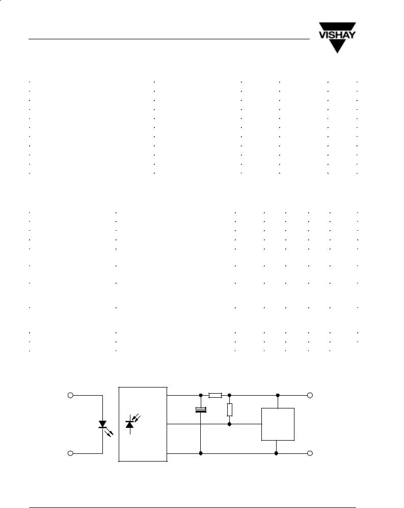
Block Diagram
|
|
|
2 |
Input |
|
Control |
VS |
|
|
||
|
Circuit |
|
|
|
|
80 kW |
|
|
|
|
|
|
|
|
3 |
PIN |
|
|
OUT |
|
|
|
|
|
AGC |
Band |
Demodu- |
|
Pass |
lator |
|
|
|
||
|
|
|
1 |
|
|
|
GND |
|
|
|
94 8136 |
Document Number 82035 |
www.vishay.com |
Rev. 8, 02-Apr-01 |
1 (8) |
TSOP17..KS1
Vishay Telefunken
Absolute Maximum Ratings
Tamb = 25_C
Parameter |
Test Conditions |
Symbol |
Value |
Unit |
Supply Voltage |
(Pin 2) |
VS |
±0.3...6.0 |
V |
Supply Current |
(Pin 2) |
IS |
5 |
mA |
Output Voltage |
(Pin 3) |
VO |
±0.3...6.0 |
V |
Output Current |
(Pin 3) |
IO |
5 |
mA |
Junction Temperature |
|
Tj |
100 |
°C |
Storage Temperature Range |
|
Tstg |
±25...+85 |
°C |
Operating Temperature Range |
|
Tamb |
±25...+85 |
°C |
Power Consumption |
(Tamb x 85 °C) |
Ptot |
50 |
mW |
Soldering Temperature |
t x 5 s |
Tsd |
260 |
°C |
Basic Characteristics
Tamb = 25_C
Parameter |
|
|
|
|
Test Conditions |
Symbol |
Min |
Typ |
Max |
Unit |
||||||
Supply Current (Pin 2) |
VS = 5 V, Ev = 0 |
|
|
|
|
|
ISD |
0.4 |
0.6 |
1.5 |
mA |
|||||
|
VS = 5 V, Ev = 40 klx, sunlight |
ISH |
|
1.0 |
|
mA |
||||||||||
Supply Voltage (Pin 2) |
|
|
|
|
|
|
|
|
|
|
|
VS |
4.5 |
|
5.5 |
V |
Transmission Distance |
Ev = 0, test signal see fig.7, |
d |
|
35 |
|
m |
||||||||||
|
IR diode TSAL6200, IF = 400 mA |
|
|
|
|
|
||||||||||
Output Voltage Low (Pin 3) |
I |
OSL |
= 0.5 mA,E |
e |
= 0.7 mW/m2, |
V |
|
|
250 |
mV |
||||||
|
|
|
|
|
|
|
|
OSL |
|
|
|
|
||||
|
f = fo, tp/T = 0.4 |
|
|
|
|
|
|
|
|
|
|
|||||
Irradiance (30 ± 40 kHz) |
Pulse width tolerance: |
|
E |
|
0.35 |
0.5 |
mW/m2 |
|||||||||
|
tpi ± 5/fo < tpo < tpi + 6/fo, |
e min |
|
|
|
|
||||||||||
|
|
|
|
|
|
|||||||||||
|
test signal (see fig.7) |
|
|
|
|
|
|
|||||||||
Irradiance (56 kHz) |
Pulse width tolerance: |
|
E |
|
0.4 |
0.6 |
mW/m2 |
|||||||||
|
tpi ± 5/fo < tpo < tpi + 6/fo, |
e min |
|
|
|
|
||||||||||
|
|
|
|
|
|
|||||||||||
|
test signal (see fig.7) |
|
|
|
|
|
|
|||||||||
Irradiance |
t |
pi |
± 5/f < t |
po |
< t |
pi |
+ 6/f |
o |
E |
30 |
|
|
W/m2 |
|||
|
|
|
o |
|
|
|
e max |
|
|
|
|
|||||
Directivity |
Angle of half transmission distance |
ϕ1/2 |
|
±45 |
|
deg |
||||||||||
Application Circuit
|
|
|
100 W *) |
+5V |
|
2 |
|
|
|
|
|
|
|
|
|
TSOP17.. |
4.7 mF *) |
|
>10 kW |
|
|
|
|
|
TSAL62.. |
|
Out |
|
optional |
3 |
|
mC |
||
|
|
|
||
|
|
|
**) |
|
|
1 |
|
|
GND |
96 12108 |
|
|
|
|
*) recommended to suppress power supply disturbances
**) The output voltage should not be hold continuously at a voltage below 3.3V by the external circuit.
www.vishay.com |
Document Number 82035 |
2 (8) |
Rev. 8, 02-Apr-01 |
TSOP17..KS1
Vishay Telefunken
Suitable Data Format
The circuit of the TSOP17..KS1 is designed in that way that unexpected output pulses due to noise or disturbance signals are avoided. A bandpassfilter, an integrator stage and an automatic gain control are used to suppress such disturbances.
The distinguishing mark between data signal and disturbance signal are carrier frequency, burst length and duty cycle.
The data signal should fullfill the following condition:
•Carrier frequency should be close to center frequency of the bandpass (e.g. 38kHz).
•Burst length should be 10 cycles/burst or longer.
•After each burst which is between 10 cycles and 70 cycles a gap time of at least 14 cycles is neccessary.
•For each burst which is longer than 1.8ms a corresponding gap time is necessary at some time in the data stream. This gap time should have at least same length as the burst.
•Up to 1400 short bursts per second can be received continuously.
Some examples for suitable data format are:
NEC Code, Toshiba Micom Format, Sharp Code, RC5 Code, RC6 Code, R±2000 Code, Sony Format (SIRCS).
When a disturbance signal is applied to the TSOP17..KS1 it can still receive the data signal. However the sensitivity is reduced to that level that no unexpected pulses will occure.
Some examples for such disturbance signals which are suppressed by the TSOP17..KS1 are:
•DC light (e.g. from tungsten bulb or sunlight)
•Continuous signal at 38kHz or at any other frequency
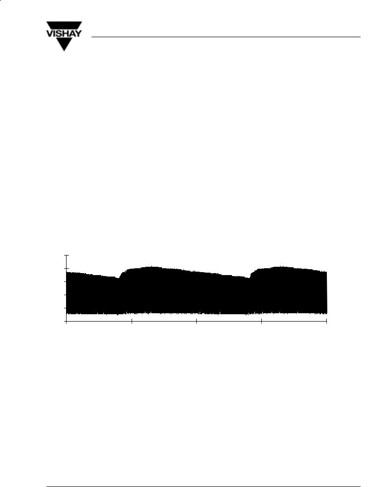
•Signals from fluorescent lamps with electronic ballast (an example of the signal modulation is in the figure below).
0 |
5 |
10 |
15 |
20 |
time [ms]
IR Signal from Fluorescent Lamp with low Modulation
Document Number 82035 |
www.vishay.com |
Rev. 8, 02-Apr-01 |
3 (8) |
 Loading...