


HCD GR3
Table of contents
 Loading...
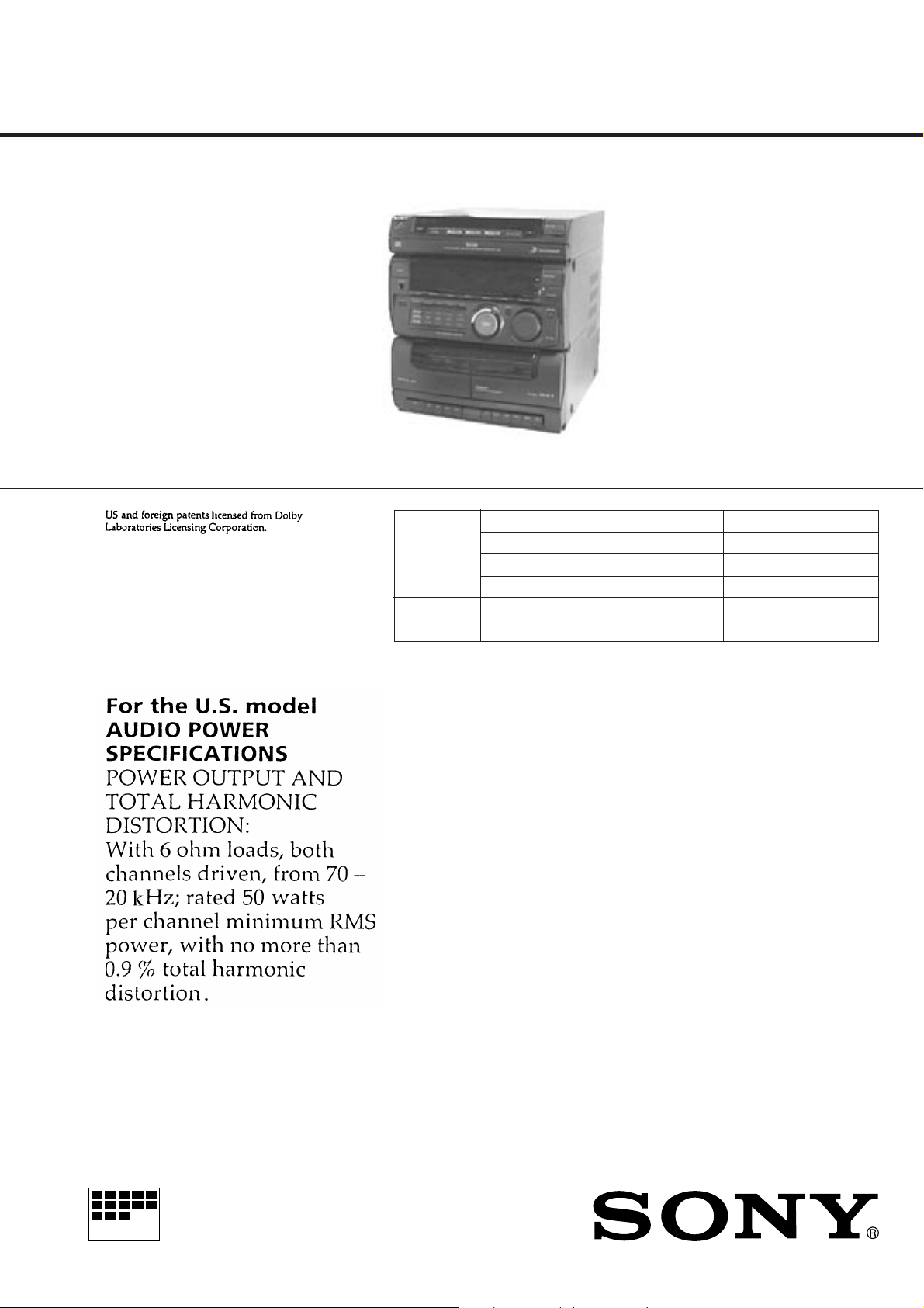
HCD-GR3/RX30
SERVICE MANUAL
HCD-GR3/RX30 is the tuner, deck, CD and amplifier section in MHC-GR3/RX30.
Dolby noise reduction manufactured under license
from Dolby Laboratories Licensing Corporation.
“DOLBY” and the double-D symbol a are trademarks of Dolby Laboratories Licensing Corporation.
* Manufactured under license from Dolby Laborato-
ries Licensing Corporation. “Dolby”, the double-D
symbol a are “Pro Logic” are trademarks of Dolby
Laboratories Licensing Corporation.
Photo: HCD-RX30
Model Name Using Similar Mechanism HCD-H991AV
CD
SECTION
TAPE
DECK
SECTION
CD Mechanism Type CDM38-5BD19FK
Base Unit Type BU-5BD19
Optical Pick-up Type KSS-213B/K-N
Model Name Using Similar Mechanism HCD-D270/G3100/N255
Tape Transport Mechanism Type TCM-YSW47C24
SPECIFICATIONS
US Model
Canadian Model
AEP Model
UK Model
HCD-RX30
E Model
Australian Model
HCD-GR3
CD player section
System Compact disc and digital
audio system
Laser Semiconductor laser
Laser output Max. 44.6µ W*
* This output is the value
measured at a distance of
200 mm from the
objective lens surface on
the Optical Pick-up Block
with 7 mm aperture.
Wavelength 780 – 790 nm
Tuner section
FM stereo, FM/AM superheterodyne
tuner
FM tuner section
Tuning range 87.5 – 108.0 MHz
Antenna FM lead antenna
Antenna terminals
75 ohm unbalanced
Intermediate frequency
10.7 MHz
AM tuner section
Tuning range
US, Canadian models:
AM: 531 – 1,710 kHz (with the
tuning interval set at 9 kHz)
530 – 1,710 kHz
(with the tuning interval set
at 10 kHz)
German models:
AM: 531 – 1,602 kHz (with the
interval set at 9 kHz)
COMPACT DISC DECK RECEIVER
AEP, UK, East European models:
MW: 531 – 1,602 kHz (with the
interval set at 9 kHz)
LW: 153 – 279 kHz (with the
interval set at 3 kHz)
Other models:
AM: 531 – 1,602 kHz (with the
tuning interval set at 9 kHz)
530 – 1,710 kHz (with the
tuning interval set at 10 kHz)
Antenna AM loop antenna,
Externalantenna terminals
Intermediate frequency
450 kHz
Amplifier section
US, Canadian models:
Continuous RMS power output
60W+60W (6 ohms at
1 kHz, 5% THD)
— Continued on next page —
MICROFILM
— 1 —
AEP, UK, German, East European models:
DIN power output
40W+40W (6 ohms at
1 kHz, DIN)
Continuous RMS power output
50W+50W (6 ohms at
1 kHz, 10% THD)
Music power output
85W+85W (6 ohms at
1 kHz, 10% THD)
Other models:
Peak music power output
800W
Continuous RMS power output
50W+50W (6 ohms at
1 kHz, 10% THD)
Inputs
VIDEO (phono jacks):
voltage 250 mV,
impedance 47 kilohms
Outputs
PHONES (stereo phone jack):
accepts headphones of
8 ohms or more.
SPEAKER: accepts impedance of 6 to
16 ohms.
SUPER WOOFER:
Tape player section
Recording system
Frequency response
Wow and flutter
General
Power requirements
US, Canadian, Mexican models:
AEP, UK, German, East European models:
Voltage 1V, impedance
1 kilo ohms.
4-track 2-channel stereo
(DOLBY NR OFF)
40 – 13,000 Hz (±3 dB),
using Sony TYPE I cassette
40 – 14,000 Hz (±3 dB),
using Sony TYPE II cassette
±0.15% W. Peak (IEC)
0.1% W. RMS (NAB)
±0.2% W. Peak (DIN)
120V AC, 60 Hz
220 – 230V AC, 50/60 Hz
South Africa model:
220 – 240V AC, 50/60 Hz
Australian model:
240V AC, 50/60 Hz
Other models:
110 – 120V or 220 – 240V
AC, 50/60 Hz
Adjustable with the voltage
selector
Power consumption
US model: 105W
Canadian model: 115 W
Other models: 95W
Dimensions Approx. 280 x 330 x 360 mm
(11 1/8 x 13 x 14 1/4 in)
(w/h/d) incl.
projecting parts and controls
Mass Approx. 7 kg (15 lb 7 oz)
Design and specifications are subject to change
without notice.
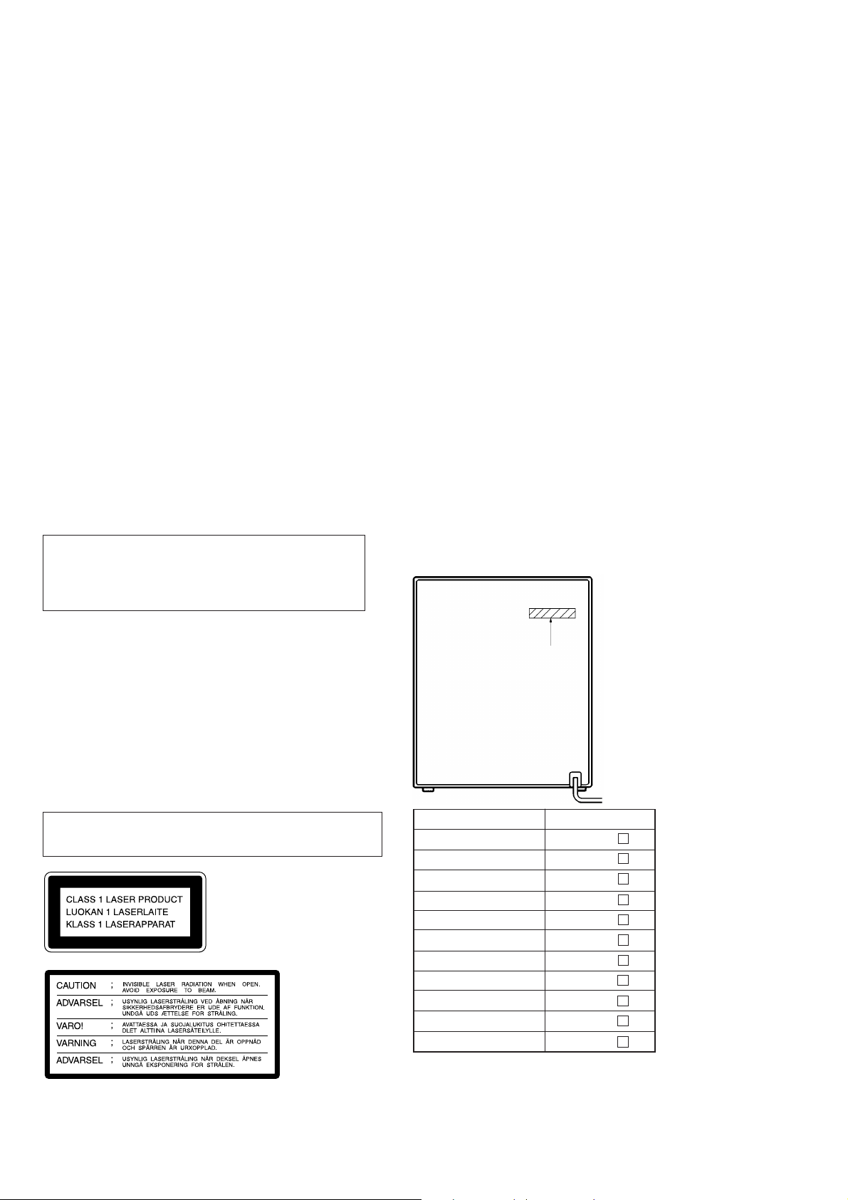
CAUTION
Use of controls or adjustments or performance of procedures
other than those specified herein may result in hazardous radiation exposure.
Notes on chip component replacement
• Never reuse a disconnected chip component.
• Notice that the minus side of a tantalum capacitor may be
damaged by heat.
Flexible Circuit Board Repairing
• Keep the temperature of soldering iron around 270˚C
during repairing.
• Do not touch the soldering iron on the same conductor of the
circuit board (within 3 times).
• Be careful not to apply force on the conductor when soldering
or unsoldering.
Laser component in this product is capable of emitting radiation
exceeding the limit for Class 1.
This appliance is classified as
a CLASS 1 LASER product.
The CLASS 1 LASER PRODUCT MARKING is located on
the rear exterior.
This caution
label is located
inside the unit.
MODEL IDENTIFICATION
— BACK PANEL —
Parts No.
MODEL
GR3 : E model
GR3 : AUS model
GR3 : MX model
GR3 : AR model
GR3 : SAF model
RX30 : US model
RX30 : CND model
RX30 : AEP model
RX30 : G model
RX30 : UK model
RX30 : EE model
4-988-804-0
4-988-804-1
4-988-804-2
4-988-804-3
4-988-804-4
4-988-810-0
4-988-810-1
4-988-811-0
4-988-811-1
4-988-811-2
4-988-811-3
• Abbreviation
CND : Canadian model
G : German model
AUS : Australian model
AR : Argentine model
SAF : South African model
MX : Mexican model
EE : East European model
PARTS No.
— 2 —
SAFETY CHECK-OUT
TABLE OF CONTENTS
After correcting the original service problem, perform the following safety checks before releasing the set to the customer:
Check the antenna terminals, metal trim, “metallized” knobs, screws,
and all other exposed metal parts for A C leakag e. Check leakage as
described below.
LEAKAGE
The AC leakage from any exposed metal part to earth Ground and
from all exposed metal parts to any exposed metal part having a
return to chassis, must not exceed 0.5 mA (500 microampers). Leakage current can be measured by any one of three methods.
1. A commercial leakage tester, such as the Simpson 229 or RCA
WT-540A. Follow the manufacturers’ instructions to use these
instruments.
2. A battery-operated AC milliammeter. The Data Precision 245
digital multimeter is suitable for this job.
3. Measuring the v oltage drop across a resistor by means of a V OM
or battery-operated AC voltmeter. The “limit” indication is 0.75
V, so analog meters must have an accurate low-voltage scale.
The Simpson 250 and Sanwa SH-63Trd are examples of a passive VOM that is suitable. Nearly all battery operated digital
multimeters that have a 2V AC range are suitable. (See Fig. A)
To Exposed Metal
Parts on Set
0.15µF
1.5k
Ω
Earth Ground
AC
voltmeter
(0.75V)
1. SERVICING NOTE
.......................................................... 4
2. GENERAL .......................................................................... 5
3. DISASSEMBLY
3-1. Loading Panel ....................................................................... 7
3-2. Front Panel ........................................................................... 7
3-3. TC Mechanism Deck ............................................................ 8
3-4. CD SW Board , Panel Board.................................................8
3-5. Disc Tray ............................................................................. 9
4. MECHANICAL ADJUSTMENTS ..........................10
5. ELECTRICAL ADJUSTMENTS ............................... 10
6. DIAGRAMS
6-1. Circuit Boards Location ...................................................... 16
6-2. Brock Diagrams
• Tuner Section................................................................... 17
• Deck Section .................................................................... 19
• CD Section ....................................................................... 21
• Main Section .................................................................... 23
6-3. Printed Wiring Board —Tuner Section —.......................... 25
6-4. Schematic Diagram — Tuner Section —............................ 26
6-5. Printed Wiring Board — Main Section —.......................... 28
6-6. Schematic Diagram — Main Section — ............................ 31
6-7. Schematic Diagram — Deck Section — ............................ 36
6-8. Printed Wiring Board — CD Motor Section —.................. 39
6-9. Schematic Diagram — CD Motor Section — .................... 40
6-10. Schematic Diagram — CD Section —............................. 42
6-11. Printed Wiring Board — CD Section — .......................... 45
6-12. Printed Wiring Board — Panel Section —....................... 47
6-13. Schematic Diagram — Panel Section — ......................... 49
6-14. IC Pin Functions ............................................................... 51
6-15. IC Block Diagrams ........................................................... 55
Fig. A. Using an AC voltmeter to check AC leakage.
SAFETY-RELATED COMPONENT WARNING !!
COMPONENTS IDENTIFIED BY MARK ! OR DO TTED LINE
WITH MARK ! ON THE SCHEMATIC DIAGRAMS AND IN
THE PARTS LIST ARE CRITICAL TO SAFE OPERATION.
REPLACE THESE COMPONENTS WITH SONY PARTS
WHOSE PART NUMBERS APPEAR AS SHOWN IN THIS
MANUAL OR IN SUPPLEMENTS PUBLISHED BY SONY.
7. EXPLODED VIEWS
7-1. Case Section........................................................................ 59
7-2. Front Panel Section 1 .......................................................... 60
7-3. Front Panel Section 2 .......................................................... 61
7-4. Back Panel Section ............................................................. 62
7-5. CD Mechanism Section 1 (CDM38-5BD19)...................... 63
7-6. CD Mechanism Section 2 (CDM38-5BD19)...................... 64
7-7. Base Unit Section (BU-5BD19)..........................................65
7-8. TC Mechanism Section 1 (TCM-YSW47C24)...................66
7-9. TC Mechanism Section 2 (TCM-YSW47C24)...................67
7-10. TC Mechanism Section 3 (TCM-YSW47C24) ................ 68
8. ELECTRICAL PARTS LIST ........................................ 69
ATTENTION AU COMPOSANT AYANT RAPPORT
À LA SÉCURITÉ!!
LES COMPOSANTS IDENTIFIÉS P AR UNE MARQUE ! SUR
LES DIAGRAMMES SCHÉMATIQUES ET LA LISTE DES
PIÈCES SONT CRITIQUES POUR LA SÉCURITÉ DE
FONCTIONNEMENT . NE REMPLA CER CES COMPOSANTS
QUE PAR DES PIÈCES SONY DONT LES NUMÉROS
SONT DONNÉS DANS CE MANUEL OU DANS LES
SUPPLÉMENTS PUBLIÉS PAR SONY.
— 3 —
SECTION 1
SERVICING NOTE
NOTES ON HANDLING THE OPTICAL PICK-UP BLOCK
OR BASE UNIT
The laser diode in the optical pick-up block may suffer electrostatic
break-down because of the potential difference generated by the
charged electrostatic load, etc. on clothing and the human body.
During repair, pay attention to electrostatic break-down and also
use the procedure in the printed matter which is included in the
repair parts.
The flexible board is easily damaged and should be handled with
care.
HOW TO OPEN THE DISC TRAY WHEN POWER SWITCH
TURNS OFF
1
Remove the Case.
NOTES ON LASER DIODE EMISSION CHECK
The laser beam on this model is concentrated so as to be focused on
the disc reflective surface by the objective lens in the optical pickup block. Therefore, when checking the laser diode emission, observe from more than 30 cm away from the objective lens.
LASER DIODE AND FOCUS SEARCH OPERATION
CHECK
Carry out the “S curve check” in “CD section adjustment” and check
that the S curve waveform is output three times.
Switching the channel step 9 KHz/10 KHz
Press ENTER/NEXT button and PO WER button simultaneously
to switch the AM channel step 9 KHz and 10 KHz. Be sure not to
change with carelessness.
3
Pull-out the disc tray.
FL Display Tube, LED All Lit and Key Check mode
When the TUNER/BAND , DISPLAY , and MENU 2 buttons
are pressed simultaneously, the FL display tube and LEDs will all
light up. Press any button to enter the key check mode.
When the key check mode is entered, the FL display tube displays
“KEY 1 0 0”. Each time a button is pressed, the counter increases
in the following order, KEY 2 n KEY 3 n KEY 4.
If buttons already pressed once are pressed again, the counter will
not increase. When the VOLUME knob is rotated in the + direction, the count increases in the following order.
0 0 n 0 1 n 0 2.
When rotated in the – direction, it decreases in the following order.
0 0 n 0 9 n 0 8.
To exit form the test mode, press the TUNER/BAND , DISPLAY , MENU 2 buttons simultaneously again.
2
Turn the cam to the
direction of arrow.
How to reset all
Pressing the TUNER/BAND , DISPLAY and MENU 3 buttons simultaneously, all are rest and returned to as when the was
shipped.
— 4 —
SECTION 2
GENERAL
This section is extracted from
instruction manual.
— 5 —
— 6 —
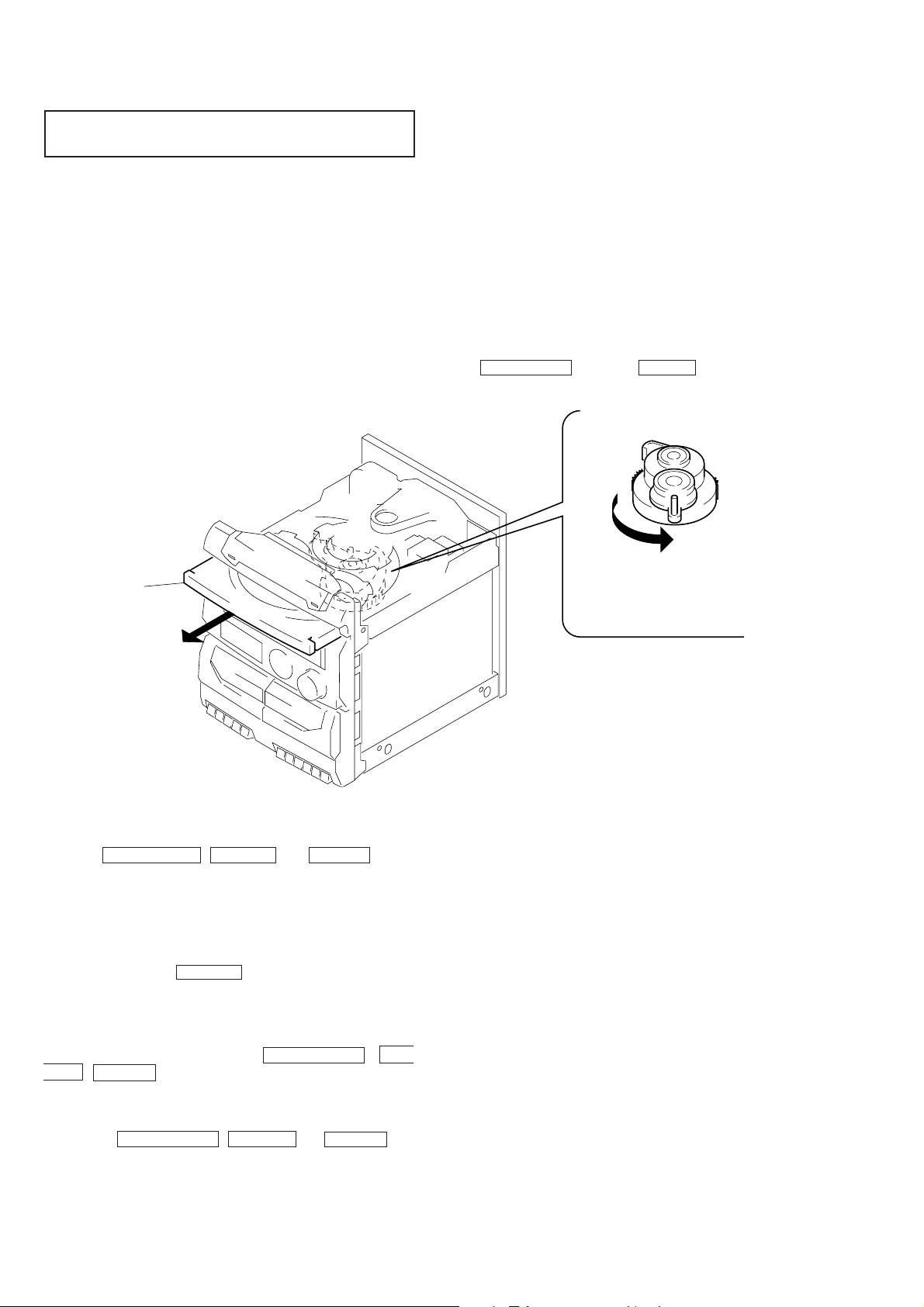
SECTION 3
DISASSEMBLY
Note: Follow the disassembly procedure in the numerical order given.
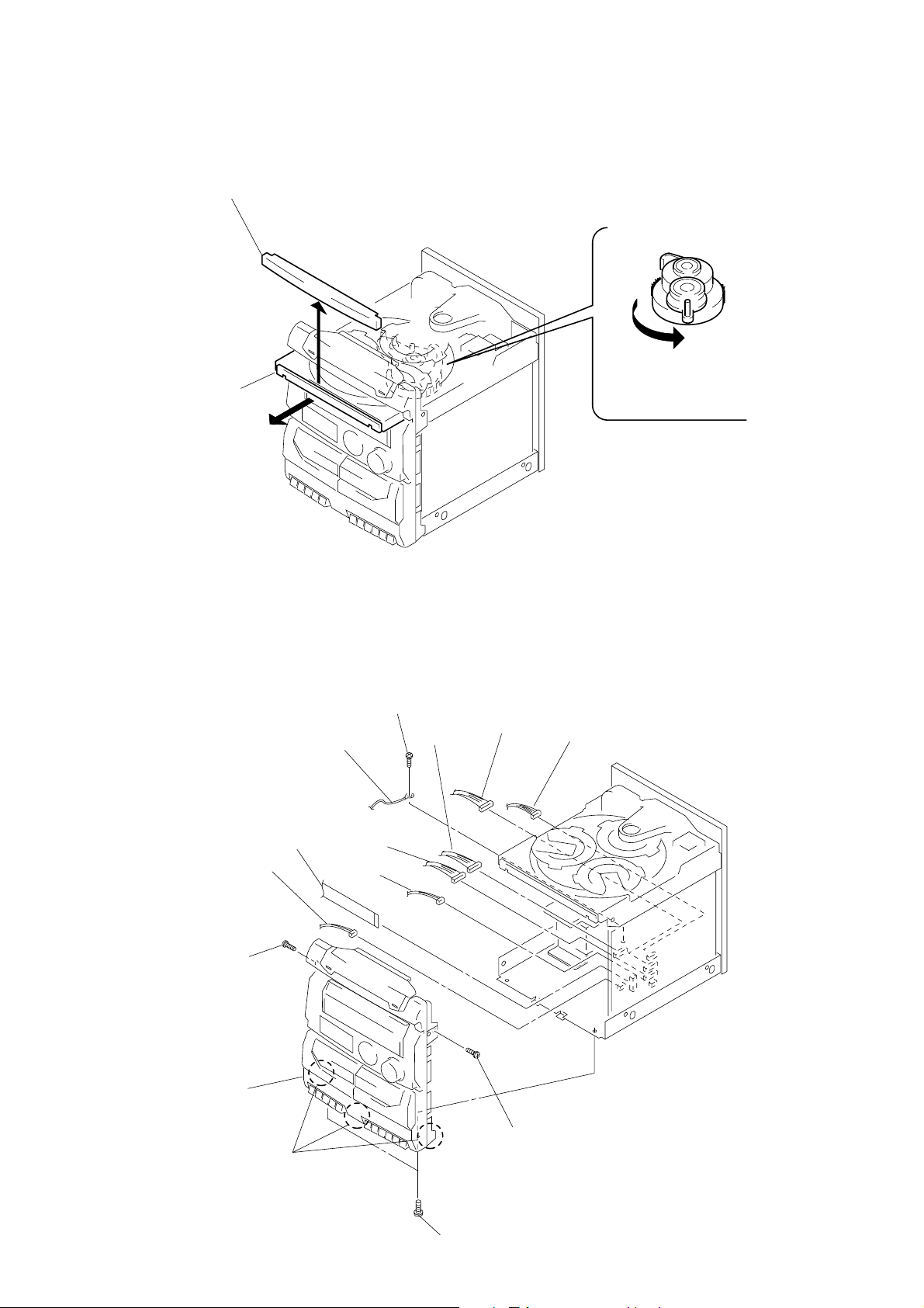
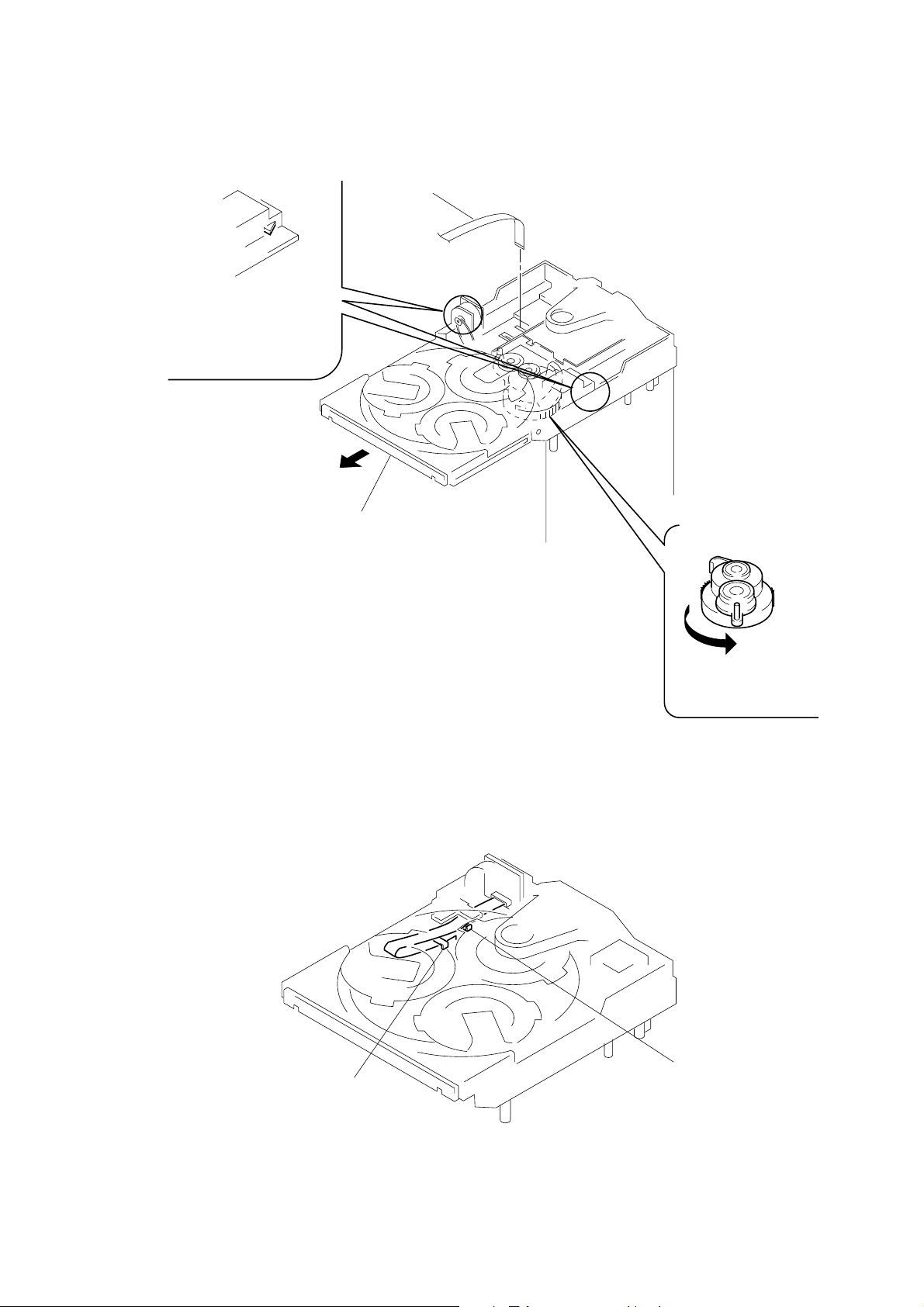
3-1. LOADING PANEL
3
Loading panel
2
Pull-out the disc tray.
1
Turn the cam to the
direction of arrow.
3-2. FRONT PANEL
1
Remove the connectors.
(Main board: CN301, CN302, CN303, CN304, CN305, CN306, CN701)
6
Screw
(BVTP3x8)
CN302
CN304
3
Screw
(BVTP3x8)
CN701
7
Wire
CN306
CN303
CN305
CN301
8
Front panel
assembly
5
claws
4
Two screws
(+BVTP3x8)
— 7 —
2
Screw
(BVTP3x8)
3-3. TC MECHANISM DECK
1
Push the EJECT button.
2
Two cassette lid
4
TC Mechanism deck
3
Six screws
(BVTP2.6x8)
3-4. CD SW BOARD AND PANEL BOARD
0
Two claws
4
Four screws
(BVTP2.6x8)
2
Nut
1
Knob (VOL)
!™
Claw
5
Five screws
(BVTP2.6x8)
8
claw
6
Two screws
(BVTP2.6x8)
3
Six screws
(BVTP2.6x8)
9
CD SW board
— 8 —
!£
Panel board
7
HP board
!¡
Two claws
3-5. DISC TRAY
(Perform after removing the front panel.)
4
Two claws
2
5
3
Flat type wire (8 core)
Pull-out the disc tray.
Remove the disc tray.
Note: When installing the Disc tray, pull around the flat type wire to
pass through the claw
A
and claw B, as shown in the figure.
claw
A
1
Turn the cam to the
direction of arrow.
claw
B
— 9 —
SECTION 4
MECHANICAL ADJUSTMENTS
SECTION 5
ELECTRICAL ADJUSTMENTS
PRECAUTION
1. Clean the following parts with a denatured alcohol-moistened
swab :
record/playback heads pinch rollers
erase head rubber belts
capstan idlers
2. Demagnetize the record/playback head with a head demagnetizer.
3. Do not use a magnetized screwdriver for the adjustments.
4. After the adjustments, apply suitable locking compound to the
parts adjusted.
5. The adjustments should be performed with the rated power supply voltage unless otherwise noted.
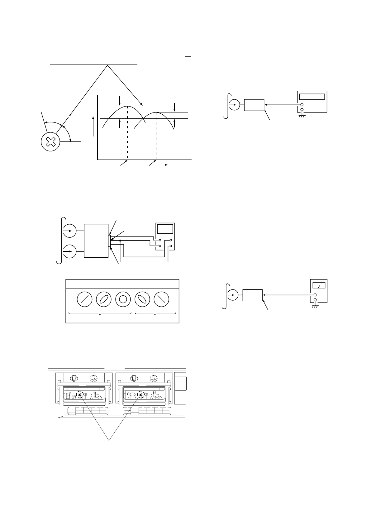
Torque Measurement
Torque Torque meter
FWD
FWD
back tension
FF/REW
FWD tension
CQ-102C
CQ-102C
CQ-201B
CQ-403A
Meter reading
30 to 80g • cm
(0.41 – 1.11 oz • inch)
1.5 to 5.5g • cm
(0.02 – 0.08 oz • inch)
55 to 130g • cm
(0.76 – 1.80 oz • inch)
100g or more
(3.53 oz or more)
DECK SECTION 0 dB=0.775V
1. Demagnetize the record/playback head with a head damagnetizer .
(Do not bring the head demagnetizer close to the erase head.)
2. Do not use a magnetized screwdriver for the adjustments.
3. After the adjustments, apply suitable locking compound to the
parts adjusted.
4. The adjustments should be performed with the rated power supply voltage unless otherwise noted.
5. The adjustments should be performed in the order given in this
service manual. (As a general rule, playback circuit adjustment
should be completed before performing recording circuit adjustment.)
6. The adjustments should be performed for both L-CH and R-ch.
7. Switches and controls should be set as follows unless otherwise
specified.
Tape
P-4-A100
WS-48B
P-4-L300
Record/Playback Head Azimuth Adjustment
(Deck A, Deck B)
Note : Perform this adjustments for both decks.
Procedure :
1. Mode : Playback
test tape
P-4-A100
(10kHz, –10dB)
Signal
10 kHz, –10 dB
3 kHz, 0 dB
315 Hz, 0 dB
main board
CN307
Pin
3
(L-CH)
Pin
1
(R-CH)
Used for
Azimuth Adjustment
Tape Speed Adjustment
Level Adjustment
level meter
set
main board
CN307
Pin
2
(GND)
+
–
— 10 —
2. Turn the adjustment screw and check output peaks. If the peaks
do not match for L-CH and R-CH, turn the adjustment screw so
that outputs match within 1 dB of peak.
L-CH
peak
output
level
within
1dB
within 1dB
Tape Speed Adjustment (Deck A, Deck B)
Procedure :
Mode : Playback
test tape
WS-48B
(3kHz, 0dB)
set
main board
CN307 Pin
Pin
frequency counter
1
(L-CH)
3
(R-CH)
+
–
R-CH
screw
position
peak
3. Mode : Playback
test tape
P-4-A100
(10kHz, –10dB)
in phase
L-CH
peak
main board
CN307
Pin
1
(L-CH)
Pin
2
3
(R-CH)
90˚
(GND)
L
set
R
Pin
Waveform of oscilloscope
45˚
R-CH
peak
oscilloscope
135˚ 180˚
wronggood
screw
position
1. Insert the WS-48B into the deck B, and playback.
2. Adjust the RV380 so that the frequency counter reading becomes
3000 ± 10 Hz.
3. Stop the deck B. Insert the WS-48B into the deck A to playback.
Be sure to check that the difference of the frequency compared
with the deck B becomes within +2% and –0.5%.
4. Insert the CS-123 (blank tape) into the deck A and insert the
WS-48B into the deck B, then playback them simultaneously.
Be sure to check that the deck B’s frequency counter reading
becomes 3000 ± 50 Hz.
Adjustment Location : MAIN board
Playback Level Adjustment (Deck A, Deck B)
Procedure :
Mode : Playback
test tape
P-4-L300
(315Hz, 0dB)
set
main board
CN307 Pin
Pin
1
(L-CH)
3
(R-CH)
level meter
4. After the adjustments, apply suitable locking compound to the
parts adjusted.
Adjustment Location :
Adjustment screws
REC/PB head (deck B)
or PB hear (deck A)
Deck A is RV301 (L-CH) and RV401 (R-CH),
Deck B is RV302 (L-CH) and RV402 (R-CH)
so that adjustment within the following adjustment level.
Adjustment level :
CN307 playback level: 301.5 to 338.3 mV (–8.2 to –7.2 dB)
level difference between the channels: within ±0.5 dB
Adjustment Location : MAIN board
— 11 —
Record Bias Adjustment (Deck B)
2. Mode: Playback
Procedure :
1. Mode : Record
AF OSC
attenuator
VIDEO IN
1) 315Hz
2) 10kHz
600
} 51.2 mV (–23.6 dB)
Ω
set
blank tape
CS-123
2. Mode : Playback
recorded
position
set
main board
CN307 Pin
Pin
1
(L-CH)
3
(R-CH)
level meter
Confirm playback the signal recorded in step 1 become adjustment
level as follows.
If these levels do not adjustment level, adjustment the RV304 (LCH) and R V404 (R-CH) on the main board to repeat steps 1 and 2.
recorded
portion
set
main board
CN307 Pin
Pin
1
3
level meter
(L-CH)
(R-CH)
Confirm playback the signal recorded in step 1 become adjustment
level as follows.
If these levels do not adjustment level, adjustment the RV303 (LCH) and R V403 (R-CH) on the main board to repeat steps 1 and 2.
Adjustment level :
CN307 playback level : 47.2 to 53.0 mV (–24.3 to –23.3 dB)
Adjustment level : Playback output of 10kHz level diffrence
against 315Hz reference should be ±0.5 dB.
Adjustment Location : MAIN board
Record Level Adjustment (Deck B)
Procedure :
1. Mode: Record
VIDEO IN
315Hz 51.2 mV (–23.6 dB)
AF OSC
attenuator
600
Ω
set
blank tape
CS-123
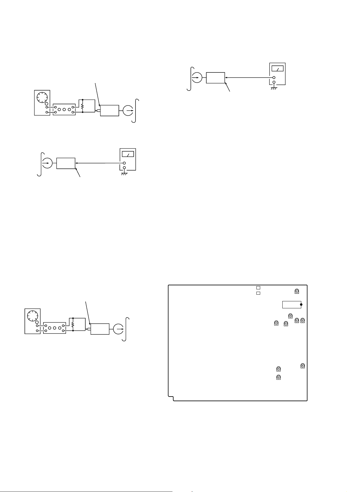
Adjustment Location
[MAIN BOARD] (Component Side)
CN308
CN307
RV401
RV404
RV301
RV304
RV303
IC303
RV403
RV380
RV
302
RV
402
— 12 —
TUNER SECTION 0dB=1µV
Note 1: As a front-end (FE1) is dif ficult to repair if f aulty , replace
it with new one.
Note 2: No adjustment is needed due to a tuner pack for except
AEP, UK, German, East European models.
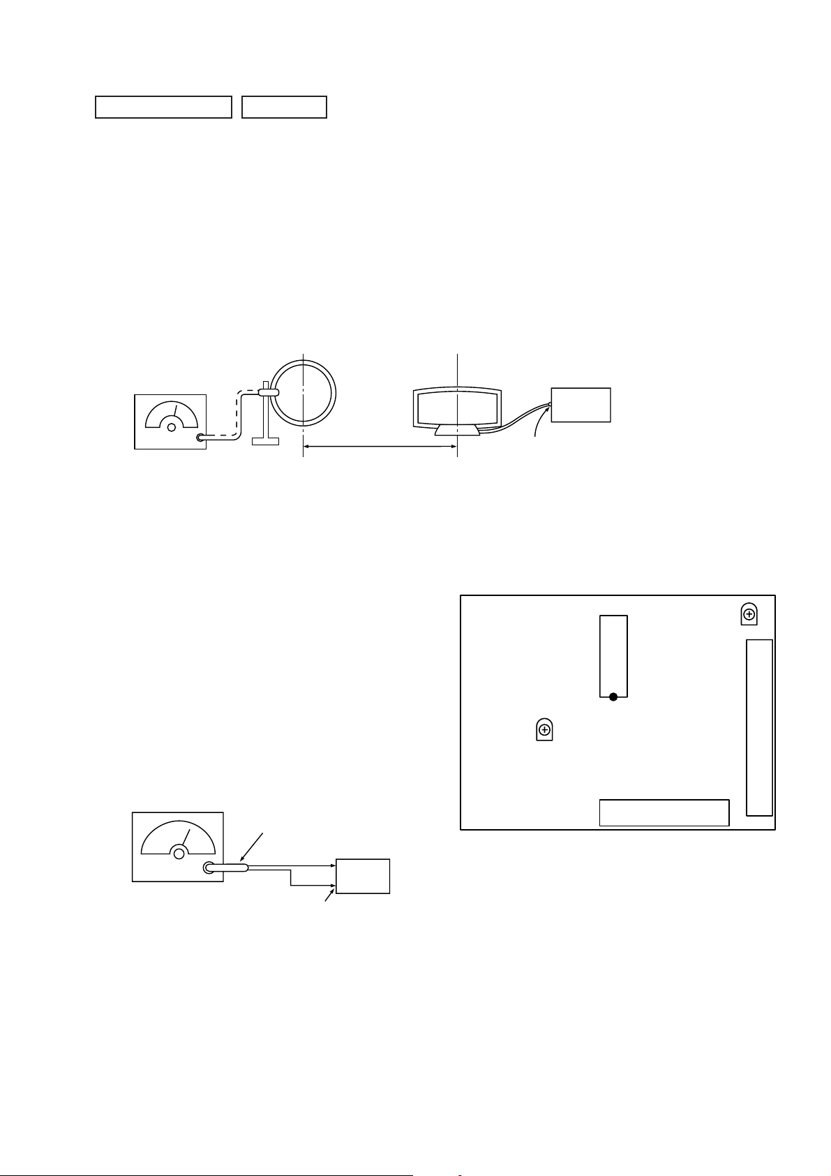
AM Tuned Level Adjustment
Note: FM Tuned Level adjustment should be performed after this
AM Tuned Level Adjustment.
Setting:
Band: AM or MW
loop antenna
loop antenna
AM RF SSG
(Supplied accessories)
set
30% amplitude
modulation by
400Hz signal
Modulation:999 kHz (at 9 kHz step)
1,050 kHz (at 10 kHz step)
60cm
Field strength dB (µV/m) = SSG output level dB (µV/m) –26dB.
Procedure:
1. Set the output of SSG so that the input level of the set becomes
55 dB.
2. Tune the set to 999 kHz or 1,050 kHz.
3. Adjust RV41 to the point (moment) when the TUNED indicator
will change from going off to going on.
Adjustment Location: TCB board
FM Tuned Level Adjustment
Note:This adjustment should be performed after the AM Tuned
Level Adjustment.
Setting:
Band: FM
FM RF SSG
75 Ω coaxial
AM antenna
terminal (TM1)
Adjustment Location
[TCB BOARD] (Component Side)
RV41
AM T uned Level
IC41
TM1
RV42
FM T uned Level
FE1
set
Carrier frequency: 98MHz
Modulation: AUDIO 1kHz, 75kHz
Output level: 25dB (at 75
deviation (100%)
Ω
open)
FM ANTENNA terminal
(TM1)
Procedure:
1. Supply a 25 dB 98 MHz signal from the ANTENNA terminal.
2. Tune the set to 98 MHz.
3. Adjust RV42 to the point (moment) when the TUNED indicator
will change from going off to going on.
— 13 —
CD SECTION
S Curve Check
Note:
1. CD Block is basically designed to operate without adjustment.
Therefore, check each item in order given.
2. Use YEDS-18 disc (3-702-101-01) unless otherwise indicated.
3. Use an oscilloscope with more than 10MΩ impedance.
4. Clean the object lens by an applicator with neutral detergent
when the signal level is low than specified value with the following checks.
5. Adjust the focus bias adjustment when optical block is replaced.
Focus Bias Adjustment
oscilloscope
BD board
TP (RF)
TP (VC)
Procedure:
1. Connect oscilloscope to test point TP (RF).
2. Tur ned Power switch on.
3. Put disc (YEDS-18) in and playback.
4. Adjust RV101 so that the waveform is clear.
(Clear RF signal waveform means that the shape “◊” can be
clearly distinguished at the center of the waveform.)
5. After adjustment, check the RF signal level.
• RF signal
VOLT/DIV: 200 mV
TIME/DIV: 500 nS
oscilloscope
BD board
TP (FEO)
TP (VC)
Procedure :
1. Connect oscilloscope to test point TP (FEO).
2. Connect between test point TP (FOK) and Ground by lead wire.
3. Tur n Power switch on.
4. Put disc (YEDS-18) in and turned Power switch on again and
actuate the focus search. (actuate the focus search when disc
table is moving in and out.)
5. Check the oscilloscope waveform (S-curve) is symmetrical between A and B. And confirm peak to peak level within 2.4 ± 0.7
Vp-p.
S-curve waveform
symmetry
A
within 2.4 ± 0.7 Vp-p
B
6. After check, remove the lead wire connected in step 2.
Note: • Try to measure several times to make sure than the ratio of
A : B or B : A is more than 10 : 7.
• T ake sweep time as long as possible and light up the brightness to obtain best waveform.
level: 1.3 ± 0.3 Vp-p
RF Level Check
oscilloscope
BD board
TP (RF)
TP (VC)
Procedure :
1. Connect oscilloscope to test point TP (RF) on BD board.
2. Tur ned Power switch on.
3. Put disc (YEDS-18) in and playback.
4. Confirm that oscilloscope waveform is clear and check RF signal level is correct or not.
Note: Clear RF signal waveform means that the shape “◊” can be
clearly distinguished at the center of the waveform.
RF signal waveform
VOLT/DIV: 200 mV
TIME/DIV: 500 nS
level: 1.3 ± 0.3 Vp-p
— 14 —
E-F Balance Check
BD board
TP (TEO)
TP (VC)
oscilloscope
Adjustment Location:
[BD BOARD] — Component Side —
RF
RV101
FOK
Procedure:
1. Connect test point TP703 (ADJ2) on Main board to Ground with
a lead wire.
2. Connect oscilloscpe to test point TP (TEO).
3. Turned Power switch on.
4. Put disc (YEDS-18) in and playback.
5. Confirm that the oscilloscope waveform is symmetrical on the
top and bottom in relation to 0Vdc, and check this level.
Traverse waveform
A
0V
B
level: 300 ± 100 mVp-p
Specified level: • x 100 = less than ± 7%
A – B
2 (A + B)
• A + B = 300 ± 100 mVp-p
6. Remove the lead wire connected in step 1.
Focus/Tracking Gain Adjustment (RV102, RV103)
RV103
IC104
TEO
VC
IC101
FEO
RV102
TEI
FEI
PCK
GND
[MAIN BOARD] — Conductor Side —
IC102
This gain has a margin, so even if it is slightly off.
There is no problem.
Therfore, do not perform this adjustment.
Please note that it should be fixed to mechanical center position
when you moved and do not know original position.
IC701
TP703
(ADJ2)
— 15 —
6-1. CIRCUIT BOARDS LOCATION
SECTION 6
DIAGRAMS
HP board
CD SW board
PANEL board
TCB board (RX30: AEP, UK, German, East European)
ENCAPSULATED COMPONENT (GR3/RX30: US, Canadian)
MAIN board
SENSOR board
TRANSFORMER board
MOTOR (TURN) board
CONNECTOR board
BD board
MOTOR (SLIDE) board
— 16 —
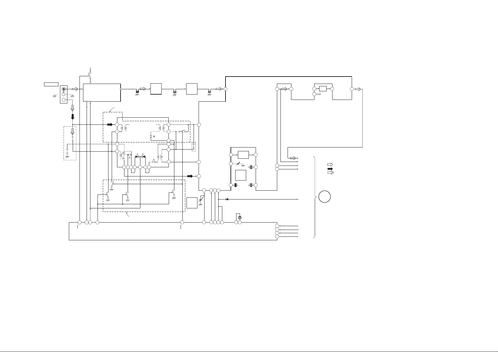
6-2. BLOCK DIAGRAMS
— TUNER SECTION — (RX30: AEP, UK, G, EE MODEL)
ST +10V
Q5
9
MW
FE1
FM FRONT END
IF OUT
Q13
MW
SW
AEP, UK, EE MODEL
6
5
3
2
26 25 24 23 22 21
Q14
LW SW
AEP, UK, EE MODEL
CF1
10.7MHz
MW/LW FRONTEND
Q12
MW
SW
TM1
ANTENNA
FM 75Ω
COAXIAL
ANT IN
F OUT
AM
G
MODEL
09
VT
191510
FM
PD1
FM OSC
HCD-GR3/RX30
IF AMP
Q1, 2
FE2
12
13
14
15
16
20
PLL
IC21
17
Q11
MW
SW
LW SW
Q9
11
MW
IF AMP
Q3, 4
G MODEL
RV42
TUNED
LEVEL
CF2
10.7MHz
CF3
10.7MHz
4
REG
29
AM OSC
27
AM RF IN
FM SD
30 14
FM
AM OSC
7
AM/FM
15
2
FM
AM MIX
VCO STOP
IF BUFF
11
1214
8
FM/AM IF
VCO STOP
1 FM IN
FM/AM MPX
AM
SD
AM
MUTE
SD
IF REQ
24 22
AM/FM
IC41
AM IF
2
12
RV41
TUNED
LEVEL
13
X42
450kHz
1 24
X IN
AM
IFT1
X OUT
10.7MHz
X21
4.5MHz
X41
X43
456kHz
5
AM IF
ST LED
9
DET
TU LED
VCO
23
CE
DI
CL
DO
MPX IN
8
7
3 ST-CE
4
5
6
OUT R
ST L
RDS SIG
STEREO
TUNED
MUTE
COM-DIN
COM-CLK
COM-DATA
OUT L
20
21
(Page 23)
LPF
RCH
A
MAIN
SECTION
18
AMP IN L
• R CH: Same as L ch
• SIGNAL PATH
: FM
: MW
: LW
• Abbreviation
G: German model.
EE : East European model.
L16
— 17 —
— 18 —
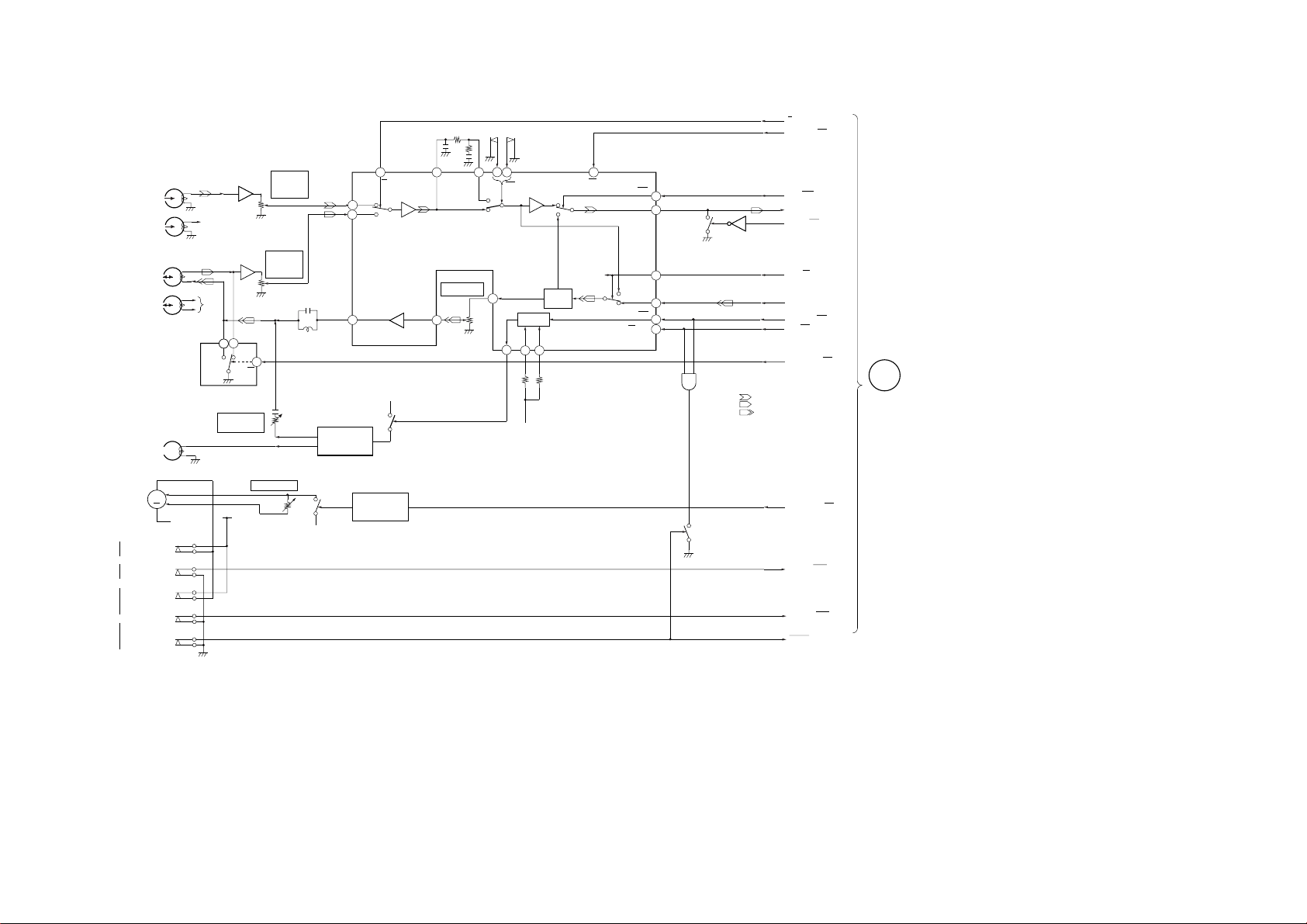
HCD-GR3/RX30
— DECK SECTION —
DECK A
S3
TYPE2
DECK B
S6
TYPE 2
A/B
DOLBY ON/OFF
REC/PB HEAD
M901
REEL/
CAPSTAN
DECK A
DECK B
HP901
PB HEAD
(DECK A)
HRP901
(DECK B)
HE901
ERASE HEAD
(MOTOR)
(MOTOR)
+
–
S1
S2
(PLAY)
S4
S5
(PLAY)
S7
(REC)
09
RV301
PLAYBACK
IC301
LEVEL
IC302
R
REC/PB
BIAS
PLAYBACK
4
RV380
TAPE SPEED
DECK A
RV302
LEVEL
DECK B
REC BIAS
Q380
– MTR
BIAS OSC
T350,Q351, 352
L
R
L
R
M
R CH
R CH
IC304
1
3
P
RV304
RECORD
ERASE BIAS
X
H
L
– MTR
+MTR
A IN
2
BIN
3
EQ OUT
13
POWER ON/OFF
Q381, 382
A/B
HEAD AMP
A +7.5V
SWITCH
IC303
Q353, 354
EQ IN
414
ABO
11
RV303
REC LEVEL
15
5
17
C IN
120/70
DOLBY NR
REC OUT
B OUT
27
BIAS SW
CROM
28 29
—
A 7.5V
PAS
DOL
70
120
10
DOLBY
TYPE B
NORM
20
NR ON/OFF
PAS/DOL
PB OUT
PB
REC IN
BIAS ON/OFF
RM ON/OFF
24
8
21
6
18
19
D452, 453
Q301
MUTE
Q451
Q450
• SIGNAL PATH
:PB (DECK A)
:PB (DECK B)
:REC (DECK B)
PAS/DOL
PB L
LM ON/OFF
REC/PB
REC L
BIAS ON/OFF
RM ON/OFF
RELAY REC/PB
POWER ON/OFF
A STOP/PLAY
B STOP/PLAY
B REC
B
MAIN
SECTION
(Page 23)
— 19 —
— 20 —
Loading...