

Siemens SAB-C513-1RN, SAB-C513A-2RM, SAB-C513A-2RN, SAB-C513A-LM, SAB-C513A-LN Datasheet
...
Data Sheet 06.96
Microcomputer Components
C51 1/C511A
C51 3/C51 3A
C51 3A-H
8-Bit CMOS Microcontroller

Data Sheet C511/C511A/C513/C513A/C513A-H
Revision History : Current Version : 06.96
Previous Releases : 02.96, 05.95
Page Subjects (changes since last revision)
Several
41
Corrections of text
Figure 22: external clock configuration corrected
8-Bit CMOS Microcontroller Family
Preliminary
C511
C511A
C513
C513A
C513A-H
●
Fully software compatible to standard 8051/8052 microcontrollers
●
Up to 12 MHz operating frequency
● Up to 12 K×8 ROM / EEPROM
●
Up to 256×8 RAM
●
Up to 256 x 8 XRAM
●
Four 8-bit ports
●
Up to three 16-bit Timers / Counters (Timer 2 with Up/Down and 16-bit Autoreload Feature)
●
Synchronous Serial Channel (SSC)
●
Optional USART
● Up to seven interrupt sources, two priority levels
●
Power Saving Modes
●
P-LCC-44 package (C513A also in P-MQFP-44 package)
●
Temperature Ranges : SAB-C511 / 511A / 513 / 513A / C513A-H
T
A
: 0 ˚C to 70 ˚C
SAF-C513A
T
A
: -40 ˚C to 85 ˚C
Semiconductor Group 3 06.96
Semiconductor Group 4
C511 / C513
The C511, C511A, C513, C513A, and C513A-H are members of a family of low cost microcontrollers, which are software compatible with the components of the SAB 8051, SAB 80C51 and
C500 families.
The first four versions contains a non-volatile read-only (ROM) program memory. The C513A-H is
a version with a 12 Kbyte EEPROM instead of ROM. This device can be used for prototype designs
which have a demand for reprogrammable on-chip code memory.
The members of the microcontroller family differ in functionality according table 1. They offer
different ROM sizes, different RAM/XRAM sizes and a different timer/USART configuration.
Common to all devices is an advanced SSC serial port, a second synchronous serial interface,
which is compatible to the SPI serial bus industry standard. The functionality of the C513A-H is a
superset of all ROM versions of the C511/C513 family.
Table 1
Functionality of the C511/C513 MCUs
1)
T0/T1 refers to the standard 8051 timer 0/1 units, T2 refers to the 8052 timer 2 unit.
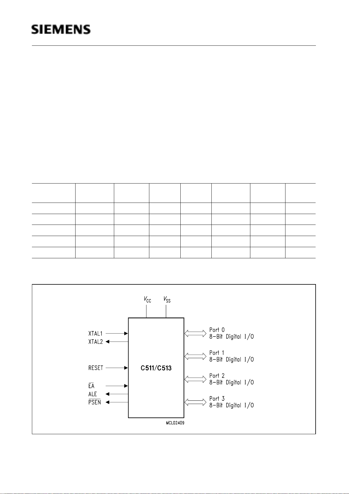
Figure 1
C511/513 Logic Symbol
Device ROM Size EEPROM
Size
RAM
Size
XRAM
Size
Timers
1)
USART SSC
C511 2.5 KB – 128 B – T0, T1 – ✓
C511A 4 KB – 256 B – T0, T1 – ✓
C513 8 KB – 256 B – T0, T1, T2 ✓✓
C513A 12, 16 KB – 256 B 256 B T0, T1, T2 ✓✓
C513A-H – 12 KB 256 B 256 B T0, T1, T2 ✓✓
C511 / C513
Semiconductor Group 5
Table 2
Ordering Information
Note : The ordering number of the ROM types (DXXXX extension) is defined after program release
(verification) of the customer.
Type Ordering
Code
Package Description
(8-Bit CMOS microcontroller)
C511-RN Q67120-DXXXX P-LCC-44 with mask-programmable ROM (2.5K), 12 MHz
C511A-RN Q67120-DXXXX P-LCC-44 with mask-programmable ROM (4K), 12 MHz
C513-1RN Q67120-DXXXX P-LCC-44 with mask-programmable ROM (8K), 12 MHz
C513A-RN Q67120-DXXXX P-LCC-44 with mask-programmable ROM (12K), 12 MHz
Q67120-DXXXX P-LCC-44 with mask-programmable ROM (12K), 12 MHz,
ext. temp. – 40 ˚C to 85 ˚C
C513A-2RN Q67120-DXXXX P-LCC-44 with mask-programmable ROM (16K), 12 MHz
Q67120-DXXXX P-LCC-44 with mask-programmable ROM (16K), 12 MHz,
ext. temp. – 40 ˚C to 85 ˚C
C513A-2RM Q67120-DXXXX P-MQFP-44 with mask-programmable ROM (16K), 12 MHz
Q67120-DXXXX P-MQFP-44 with mask-programmable ROM (16K), 12 MHz,
ext. temp. – 40 ˚C to 85 ˚C
C513A-LN Q67120-C1017 P-LCC-44 for external memory (12 MHz)
Q67120-C1035 P-LCC-44 for external memory (12 MHz),
ext. temp. – 40 ˚C to 85 ˚C
C513A-LM Q67120-C1026 P-MQFP-44 for external memory (12 MHz)
Q67120-C1036 P-MQFP-44 for external memory (12 MHz),
ext. temp. – 40 ˚C to 85 ˚C
C513A-HN Q67120-C0989 P-LCC-44 with reprogrammable EEPROM (12K), 12 MHz,
ext. temp. – 40 ˚C to 85 ˚C
Semiconductor Group 6
C511 / C513
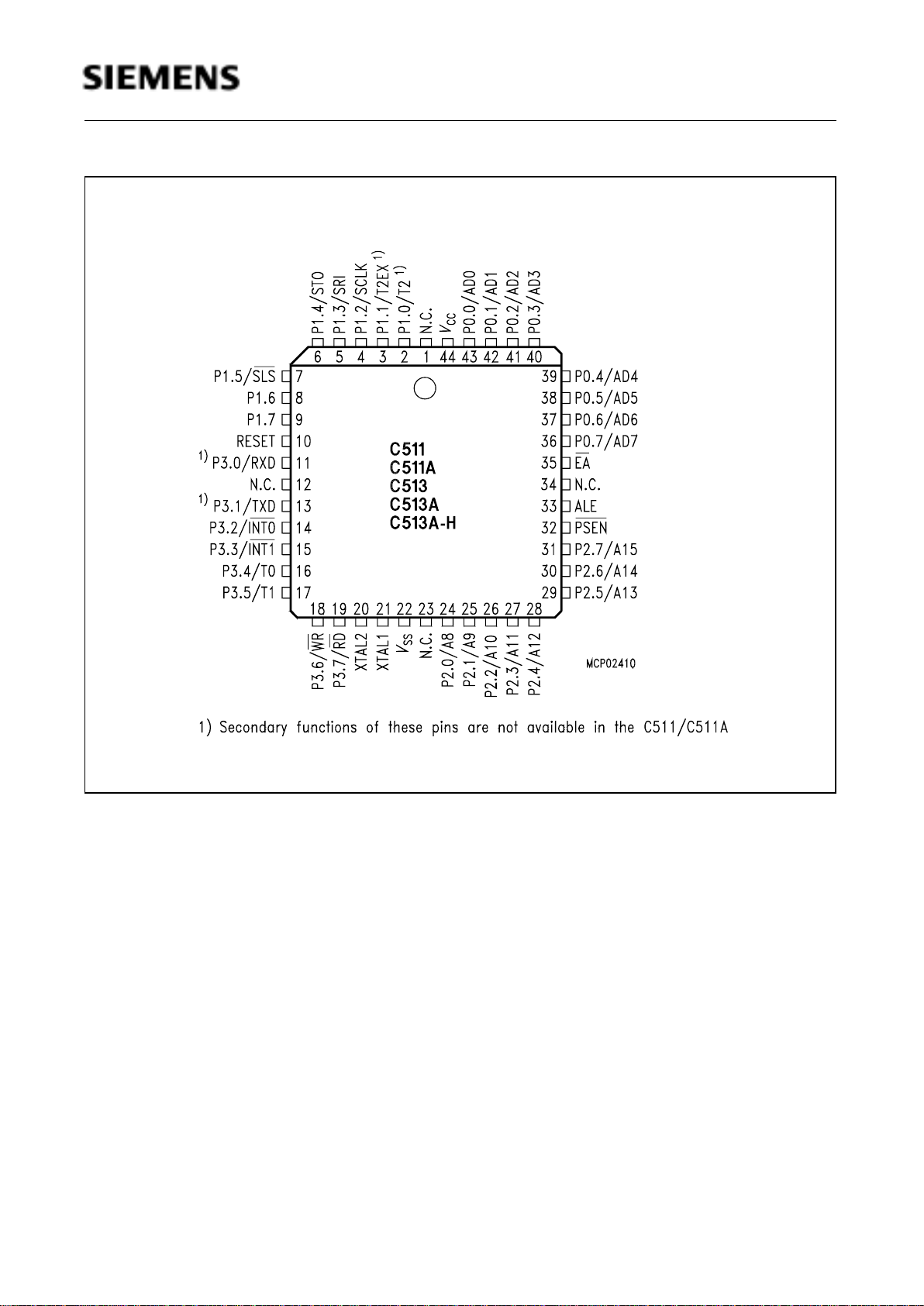
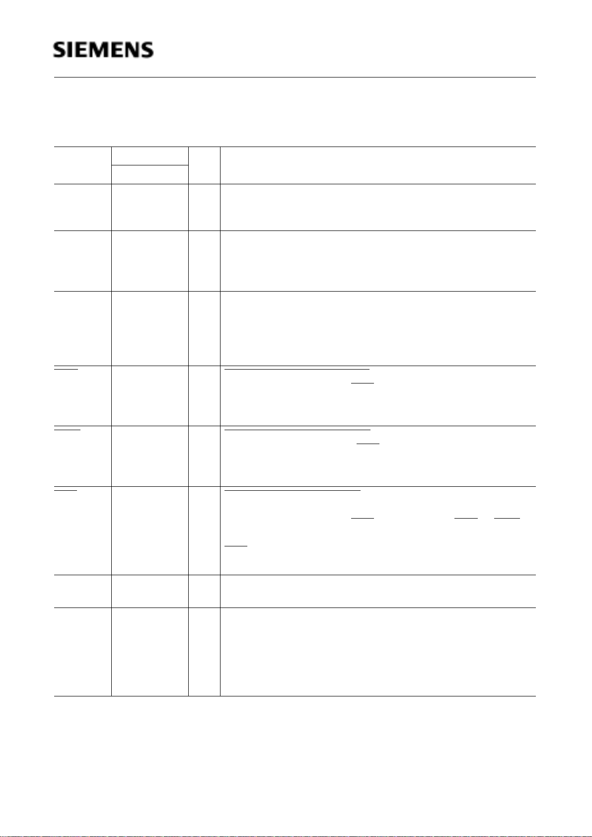
Figure 2
P-LCC-44 Package Pin Configuration (Top View)
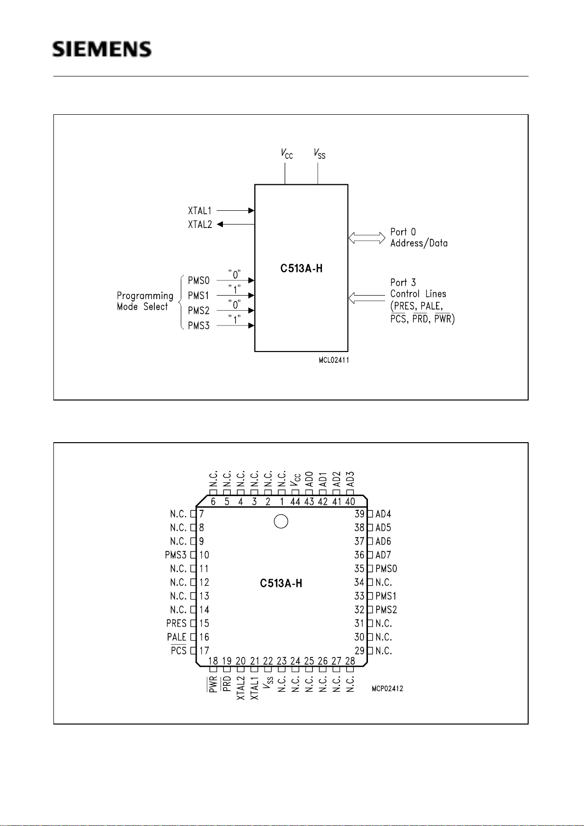
If the C513A-H is used in programming mode, the pin configuration is different to figure 2 and 3 (see
figure 5).
C511 / C513
Semiconductor Group 7
Figure 3
P-MQFP-44 Package Pin Configuration of the C513A (Top View)
Semiconductor Group 8
C511 / C513
Table 3
Pin Definitions and Functions
Symbol Pin Number I/O*) Function
P-LCC-44P-MQFP-
44
P1.7-P1.0 9-2
2
3
4
5
6
7
3-1,
44-40
40
41
42
43
44
1
I/O Port 1
is a bidirectional I/O port with internal pull-up resistors.
Port 1 pins that have 1s written to them are pulled high by
the internal pullup resistors, and in that state can be used
as inputs. As inputs, port 1 pins being externally pulled
low will source current (
I
IL
, in the DC characteristics)
because of the internal pullup resistors. Port 1 also
contains the timer 2 and SSC pins as secondary function.
In general the output latch corresponding to a secondary
function must be programmed to a one (1) for that
function to operate.
For the outputs of the SSC (SCLK, STO) special circuitry
is implemented, providing true push-pull capability. The
STO output in addition will have true tristate capability.
When used for SSC inputs, the pull-up resistors will be
switched off and the inputs will float (high ohmic inputs).
The alternate functions are assigned to port 1, as follows:
P1.0 T2 Input to counter 2
1)
P1.1 T2EX Capture -Reload trigger of timer 2
1)
Up-Down count
P1.2 SCLK SSC Master Clock Output
SSC Slave Clock Input
P1.3 SRI SSC Receive Input
P1.4 STO SSC Transmit Output
P1.5 SLS
Slave Select Input
1
)
not available in the C511/511A
*) I = Input
O = Output
C511 / C513
Semiconductor Group 9
P3.0-P3.7 11,
13-19
11
13
14
15
16
17
18
19
5, 7-13
5
7
8
9
10
11
12
13
I/O Port 3
is a bidirectional I/O port with internal pull-up resistors.
Port 3 pins that have 1s written to them are pulled high by
the internal pullup resistors, and in that state can be used
as inputs. As inputs, port 3 pins being externally pulled
low will source current (I
IL
, in the DC characteristics)
because of the internal pullup resistors. Port 3 also
contains the interrupt, timer, serial port and external
memory strobe pins that are used by various options. The
output latch corresponding to a secondary function must
be programmed to a one (1) for that function to operate.
The secondary functions are assigned to the pins of port
3 as follows:
P3.0 RXD Receiver data input (asynchronous)
or data input/output (synchronous)
of serial interface (USART)
1)
P3.1 TXD Transmitter data output (USART)
1)
(asynchronous) or clock output
(synchronous) of serial interface
P3.2 INT0
Interrupt 0 input / timer 0 gate control
P3.3 INT1
Interrupt 1 input / timer 1 gate control
P3.4 T0 Counter 0 input
P3.5 T1 Counter 1 input
P3.6 WR Write control signal : latches the data
byte from port 0 into the external
data memory
P3.7 RD Read control signal : enables the
external data memory to port 0
1
)
not available in the C511/511A
XTAL2 20 14 – XTAL2
Output of the inverting oscillator amplifier.
*) I = Input
O = Output
Table 3
Pin Definitions and Functions (cont’d)
Symbol Pin Number I/O*) Function
P-LCC-44P-MQFP-
44

Semiconductor Group 10
C511 / C513
XTAL1 21 15 – XTAL1
Input to the inverting oscillator amplifier and input to the
internal clock generator circuits.
To drive the device from an external clock source, XTAL1
should be driven, while XTAL2 is left unconnected. There
are no requirements on the duty cycle of the external
clock signal, since the input to the internal clocking
circuitry is divided down by a divide-by-two flip-flop.
Minimum and maximum high and low times as well as
rise/fall times specified in the AC characteristics must be
observed.
P2.0-P2.7 24-31 18-25 I/O Port 2
is a bidirectional I/O port with internal pullup resistors.
Port 2 pins that have 1s written to them are pulled high by
the internal pullup resistors, and in that state can be used
as inputs. As inputs, port 2 pins being externally pulled
low will source current (
I
IL
, in the DC characteristics)
because of the internal pullup resistors. Port 2 emits the
high-order address byte during fetches from external
program memory and during accesses to external data
memory that use 16-bit addresses (MOVX @DPTR). In
this application it uses strong internal pullup resistors
when issuing 1s. During accesses to external data
memory that use 8-bit addresses (MOVX @Ri), port 2
issues the contents of the P2 special function register.
PSEN
32 26 O The Program Store
Enable
output is a control signal that enables the external
program memory to the bus during external fetch
operations. It is activated every six oscillator periodes
except during external data memory accesses. Remains
high during internal program execution.
RESET 10 4 I RESET
A high level on this pin for two machine cycles while the
oscillator is running resets the device. An internal resistor
to
V
SS
permits power-on reset using only an external
capacitor to VCC.
*) I = Input
O = Output
Table 3
Pin Definitions and Functions (cont’d)
Symbol Pin Number I/O*) Function
P-LCC-44P-MQFP-
44
C511 / C513
Semiconductor Group 11
ALE 33 27 O The Address Latch Enable
output is used for latching the low-byte of the address into
external memory during normal operation. It is activated
every six oscillator periodes except during an external
data memory access.
If no external memory is used, the ALE signal generation
can be inhibited, reducing system RFI, by clearing
register bit EALE in the SYSCON register.
EA
35 29 I External Access Enable
When held at high level, instructions are fetched from the
internal ROM when the PC is less than the size of the
internal ROM : C511 0A00
H
C511A 1000
H
C513 2000
H
C513A/A-H 3000
H
C513A-2R 4000
H
When held at low level, the microcontroller fetches all
instructions from external program memory.
P0.0-P0.7 43-36 37-30 I/O Port 0
is an 8-bit open-drain bidirectional I/O port. Port 0 pins
that have 1s written to them float, and in that state can be
used as high-impendance inputs. Port 0 is also the
multiplexed low-order address and data bus during
accesses to external program or data memory. In this
application it uses strong internal pullup transistors when
issuing 1s. External pullup resistors are required during
program verification.
V
SS
22 16 – Circuit ground potential
V
CC
44 38 – Power Supply terminal for all operating modes
N.C. 1, 12,
23, 34
6, 17,
28, 39
– No connection, do not connect externally
*) I = Input
O = Output
Table 3
Pin Definitions and Functions (cont’d)
Symbol Pin Number I/O*) Function
P-LCC-44P-MQFP-
44
Semiconductor Group 12
C511 / C513
Figure 4
C513A-H Logic Symbol in Programming Mode
Figure 5
C513A-H Pin Configuration in Programming Mode (P-LCC-44)
C511 / C513
Semiconductor Group 13
Table 4
Pin Definitions and Functions in Programming Mode (C513A-H only)
Symbol Pin Number I/O*) Function
P-LCC-44
PRES 15 I Programming Interface Reset
A high level on this input resets the programming interface and
its registers to their initial state.
AD0 - AD7 43 - 36 I/O Bidirectional Address/Data Bus
AD0-7 is used to transfer data to and from the registers of the
programming interface and to read the data of the memory field
during EEPROM verification.
PALE 16 I Programming Address Latch Enable
This input is used to latch address information at AD0-7. The
trailing edge of PALE is used to latch the register addresses.
Each read or write access in programming mode must be
initiated by a PALE high pulse.
PRD
18 I Programming Read Control
A low level at this pin (and PCS
=low) enables the AD0-7 buffers
for reading of the data or control registers of the programming
interface.
PWR
19 I Programming Write Control
A low level at this pin (and PCS
=low) causes the data at AD07 to be written into the data or control registers of the
programming interface.
PCS
17 I Programming Chip Select
A low level at this pin enables the access to the registers of the
programming interface. If PCS
is active, either PRD or PWR
control whether data is read or written into the registers.
PCS
should be always deactivated between subsequent
accesses to the programming interface.
XTAL2 20 – XTAL2
Output of the inverting oscillator amplifier.
XTAL1 21 – XTAL1
Input to the inverting oscillator amplifier and input to the internal
clock generator circuits.
To drive the device from an external clock source, XTAL1
should be driven, while XTAL2 is left unconnected.
During the
device programming a clock must be always supplied.
*) I = Input
O = Output

Semiconductor Group 14
C511 / C513
PMS0
PMS1
PMS2
PMS3
35
33
32
10
I Programming Mode Select
PMS0-3 are used to put the C513A-H into the program-ming
mode. In normal mode the programming mode select pins have
the meaning as shown in the table below. PMS0-3 must be set
to the logic level as described in the table below.
V
SS
22 – Circuit ground potential
V
CC
44 – Power supply terminal for all operating modes
N.C. 1-9, 11-14,
23-31, 34
– No connection
These pins must not be connected.
*) I = Input
O = Output
Table 4
Pin Definitions and Functions in Programming Mode (C513A-H only) (cont’d)
Symbol Pin Number I/O*) Function
P-LCC-44
Normal Mode
Pin Names
Progr. Mode
Pin Names
Required
Logic Level
EA
PMS0 0
ALE PMS1 1
PSEN
PMS2 0
RESET PMS3 1

C511 / C513
Semiconductor Group 15
Functional Description
The C511/C513 microcontrollers are fully compatible to the standard 8051/80C52 and C500
microcontroller family. While maintaining all architectural and operational characteristics of the
80C52/C500 the C511/C513 incorporates enhancements such as additional internal XRAM and a
second (synchronous) serial interface unit.
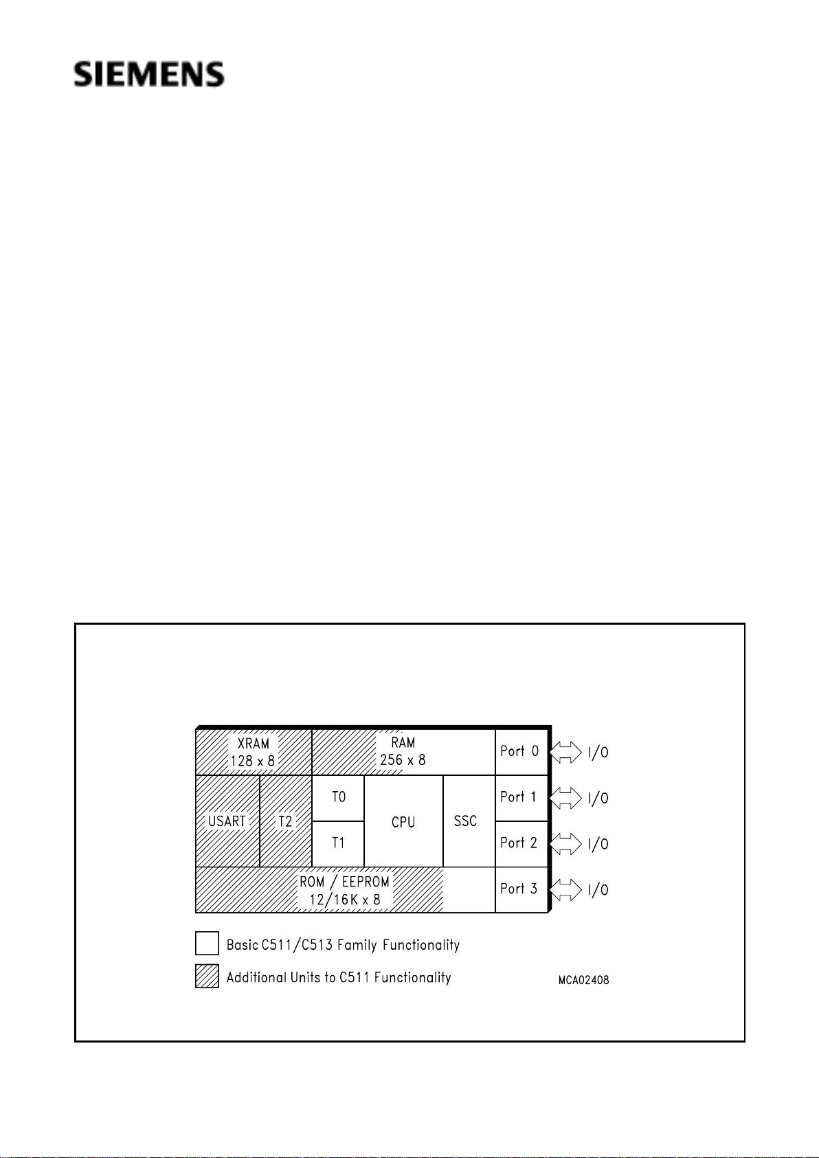
Figure 6 shows a block diagram of the C511/C513 microcontroller family.
Figure 6
Block Diagram of the C511/C513 Units

Semiconductor Group 16
C511 / C513
CPU
The C511/C513 are efficient both as a controller and as an arithmetic processor. It has extensive
facilities for binary and BCD arithmetic and for bit-handling capabilities. Efficient use of program
memory results from an instruction set consisting of 44 % one-byte, 41 % two-byte, and 15 % threebyte instructions. With a 12 MHz crystal, 58 % of the instructions execute in 1 µs.
Special Function Register PSW (Address D0H) Reset Value : 00
H
Bit Function
CY Carry Flag
AC Auxiliary Carry Flag (for BCD operations)
F0 General Purpose Flag
RS1 RS0
00
01
10
11
Register Bank select control bits
Bank 0 selected, data address 00H-07
H
Bank 1 selected, data address 08H-0F
H
Bank 2 selected, data address 10H-17
H
Bank 3 selected, data address 18H-1F
H
OV Overflow Flag
F1 General Purpose Flag
P Parity Flag
Set/cleared by hardware each instruction cycle to indicate an odd/even number of
"one" bits in the accumulator, i.e. even parity.
CY AC F0 RS1
D0
H
PSW
Bit No. 76543210
MSB
LSB
RS0 OV F1 P

C511 / C513
Semiconductor Group 17
Special Function Registers
All registers except the program counter and the four general purpose register banks reside in the
special function register area.
The 34 special function registers (SFR) include pointers and registers that provide an interface
between the CPU and the other on-chip peripherals. There are also 128 directly addressable bits
within the SFR area.
All SFRs are listed in table 5 and table 6. In table 5 they are organized in groups which refer to the
functional blocks of the C511/C513. Table 6 illustrates the contents of the SFRs, e.g. the bits of the
SFRs, in numeric order of their addresses.

Semiconductor Group 18
C511 / C513
Table 5
SFRs - Functional Blocks
Block Symbol Name Address Contents after
Reset
CPU ACC
B
DPH
DPL
PSW
SP
SYSCON
Accumulator
B-Register
Data Pointer, High Byte
Data Pointer, Low Byte
Program Status Word
Stack Pointer
System Control Reg. C511/C511A/C513
C513A/C513A-H
E0
H
1
)
F0
H
1
)
83
H
82
H
D0
H
1
)
81
H
B1
H
B1
H
00
H
00
H
00
H
00
H
00
H
07
H
101X0XXX
B
3)
101X0XX0
B
3)
Interrupt
System
IE
IP
Interrupt Enable Register
Interrupt Priority Register
A8
H
1)
B8
H
1)
00
H
X0000000
B
3)
Ports P0
P1
P2
P3
Port 0
Port 1
Port 2
Port 3
80
H
1)
90
H
1)
A0
H
1)
B0
H
1)
FF
H
FF
H
FF
H
FF
H
SSC SSCCON
STB
SRB
SCF
SCIEN
SSCMOD
SSC Control Register
SSC Transmit Buffer
SSC Receive Register
SSC Flag Register
SSC Interrupt Enable Register
SSC Mode Test Register
E8
H
1
)
E9
H
EA
H
F8
H
1
)
F9
H
EB
H
07
H
XX
H
3
)
XX
H
3
)
XXXXXX00
B
3)
XXXXXX00
B
3)
00
H
USART PCON
2)
SBUF
SCON
Power Control Register
Serial Channel Buffer Register
Serial Channel 1 Control Register
87
H
99
H
98
H
1)
0XXX0000
B
3)
XX
H
3
)
00
H
Timer 0 /
Timer 1
TCON
TMOD
TL0
TL1
TH0
TH1
Timer Control Register
Timer Mode Register
Timer 0, Low Byte
Timer 1, Low Byte
Timer 0, High Byte
Timer 1, High Byte
88
H
1)
89
H
8A
H
8B
H
8C
H
8D
H
00
H
00
H
00
H
00
H
00
H
00
H
Timer 2 T2CON
T2MOD
RC2L
RC2H
TL2
TH2
Timer 2 Control Register
Timer 2 Mode Register
Timer 2 Reload/Capture Register, Low Byte
Timer 2 Reload/Capture Register, High Byte
Timer 2 Low Byte
Timer 2 High Byte
C8
H
1)
C9
H
CA
H
CB
H
CC
H
CD
H
00
H
XXXXXXX0
B
3)
00
H
00
H
00
H
00
H
Power
Save Mode
PCON
2)
Power Control Register 87
H
0XXX0000
B
3)
1)
Bit-addressable special function registers
2)
This special function register is listed repeatedly since some bits of it also belong to other functional blocks.
3)
X means that the value is indeterminate and the location is reserved

C511 / C513
Semiconductor Group 19
Table 6
Contents of the SFRs, SFRs in Numeric Order of their Addresses
Addr Register Content
after
Reset
1)
Bit 7 Bit 6 Bit 5 Bit 4 Bit 3 Bit 2 Bit 1 Bit 0
80
H
P0 FF
H
.7 .6 .5 .4 .3 .2 .1 .0
81
H
SP 07
H
.7 .6 .5 .4 .3 .2 .1 .0
82
H
DPL 00
H
.7 .6 .5 .4 .3 .2 .1 .0
83
H
DPH 00
H
.7 .6 .5 .4 .3 .2 .1 .0
87
H
PCON 0XXX-
0000
B
SMOD – – – GF1 GF0 PDE IDLE
88
H
TCON 00
H
TF1 TR1 TF0 TR0 IE1 IT1 IE0 IT0
89
H
TMOD 00
H
GATE C/T M1 M0 GATE C/T M1 M0
8A
H
TL0 00
H
.7 .6 .5 .4 .3 .2 .1 .0
8B
H
TL1 00
H
.7 .6 .5 .4 .3 .2 .1 .0
8C
H
TH0 00
H
.7 .6 .5 .4 .3 .2 .1 .0
8D
H
TH1 00
H
.7 .6 .5 .4 .3 .2 .1 .0
90
H
P1 FF
H
– – SLS STO SRI SCLK T2EX T2
98
H
SCON 00
H
SM0 SM1 SM2 REN TB8 RB8 TI RI
99
H
SBUF XX
H
.7 .6 .5 .4 .3 .2 .1 .0
A0
H
P2 FF
H
.7 .6 .5 .4 .3 .2 .1 .0
A8
H
IE 00
H
EAL ESSC ET2 ES0 ET1 EX1 ET0 EX0
B0
H
P3 FF
H
RD WR T1 T0 INT1 INT0 TxD0 RxD0
B1
H
SYSCON
2)
1 0 EALE –0––XMAP
2)
B8
H
IP X000-
0000
B
– PSSC PT2 PS PT1 PX1 PT0 PX0
C8HT2CON 00
H
TF2 EXF2 RCLK TCLK EXEN2 TR2 C/T2 CP/
RL2
C9HT2MOD XXXX-
XXX0
B
–––––––DCEN
CA
H
RC2L 00
H
.7 .6 .5 .4 .3 .2 .1 .0
CB
H
RC2H 00
H
.7 .6 .5 .4 .3 .2 .1 .0
CC
H
TL2 00
H
.7 .6 .5 .4 .3 .2 .1 .0
CD
H
TH2 00
H
.7 .6 .5 .4 .3 .2 .1 .0
D0HPSW 00
H
CY AC F0 RS1 RS0 OV F1 P
E0
H
ACC 00
H
.7 .6 .5 .4 .3 .2 .1 .0
E8
H
SSCCON 07
H
SCEN TEN MSTR CPOL CPHA BRS2 BRS1 BRS0
E9
H
STB XX
H
.7 .6 .5 .4 .3 .2 .1 .0
EA
H
SRB XX
H
.7 .6 .5 .4 .3 .2 .1 .0
EB
H
SSCMOD 00
H 3)
00000000
F0
H
B 00
H
.7 .6 .5 .4 .3 .2 .1 .0

Semiconductor Group 20
C511 / C513
F8
H
SCF XXXX-
XX00
B
– – – – – – WCOL TC
F9
H
SCIEN XXXX-
XX00
B
––––––WCEN TCEN
1)
X means that the value is indeterminate and the location is reserved.
2)
The availability of the XMAP bit and the reset value of SYSCON depends on the specific microcontroller :
C511/C511A/C513 : 101X0XXX
B
- bit XMAP is not available
C513A/C513A-H : 101X0XX0
B
- bit XMAP is available
3)
This register ist only used for test purposes and must not be written. Otherwise unpredictable results may
occur.
Shaded registers are bit-addressable special function registers.
Table 6
Contents of the SFRs, SFRs in Numeric Order of their Addresses (cont’d)
Addr Register Content
after
Reset
1)
Bit 7 Bit 6 Bit 5 Bit 4 Bit 3 Bit 2 Bit 1 Bit 0

C511 / C513
Semiconductor Group 21
Timer/ Counter 0 and 1
Timer/Counter 0 and 1 can be used in four operating modes as listed in table 7:
Table 7
Timer/Counter 0 and 1 operating modes
In “timer” function (C/T = ‘0’) the register is incremented every machine cycle. Therefore the count
rate is f
OSC
/12.
In “counter” function the register is incremented in response to a 1-to-0 transition at its
corresponding external input pin (P3.4/T0, P3.5/T1). Since it takes two machine cycles to detect a
falling edge the max. count rate is f
OSC
/24. External inputs INT0 and INT1 (P3.2, P3.3) can be
programmed to function as a gate to facilitate pulse width measurements. Figure 7 illustrates the
input clock logic.
Figure 7
Timer/Counter 0 and 1 Input Clock Logic
Mode Description TMOD Input Clock
Gate C/T
M1 M0 internal external (max)
0 8-bit timer/counter with a
divide-by-32 prescaler
XX00
f
OSC/12 × 32
f
OSC/24 × 32
1 16-bit timer/counter X X 0 1 f
OSC/12
f
OSC/24
2 8-bit timer/counter with
8-bit auto-reload
XX10f
OSC/12
f
OSC/24
3 Timer/counter 0 used as one
8-bit timer/counter and one
8-bit timer
Timer 1 stops
XX11f
OSC/12
f
OSC/24

Semiconductor Group 22
C511 / C513
Timer / Counter 2 (not available in the C511/C511A)
Timer 2 is a 16-bit Timer/Counter with up/down count feature. It can operate either as timer or as an
event counter which is selected by bit C/T2 (T2CON.1). It has three operating modes as shown in
table 8.
Table 8
Timer/Counter 2 Operating Modes
Note: ↓ = falling edge
Mode
T2CON T2MOD
DCEN
T2CON
EXEN
P1.1/
T2EX
Remarks
Input Clock
R×CLK
or
T×CLK
CP/
RL2
TR2 internal
external
(P1.0/T2)
16-bit
Auto-
reload
0
0
0
0
0
0
0
0
1
1
1
1
0
0
1
1
0
1
X
X
X
↓
0
1
reload upon
overflow
reload trigger
(falling edge)
Down counting
Up counting
f
OSC
/12
max
f
OSC
/24
16-bit
Cap-
ture
0
0
1
1
1
1
X
X
0
1
X
↓
16-bit Timer/
Counter (only
up-counting)
capture TH2,
TL2 → RC2H,
RC2L
f
OSC
/12
max
f
OSC
/24
Baud
Rate
Gene-
rator
1
1
X
X
1
1
X
X
0
1
X
↓
no overflow
interrupt
request (TF2)
extra external
interrupt
(“Timer 2”)
f
OSC
/2
max
f
OSC
/24
off X X 0 X X X Timer 2 stops – –

C511 / C513
Semiconductor Group 23
Serial Interface (USART, not available in the C511/C511A)
The serial port is full duplex and can operate in four modes (one synchronous mode, three
asynchronous modes) as illustrated in table 9. Figure 8 illustrates the block diagram of Baudrate
generation for the serial interface.
Table 9
USART Operating Modes
Figure 8
Block Diagram of Baud Rate Generation for the Serial Interface
Mode
SCON Baudrate Description
SM0 SM1
000
f
OSC
/12 Serial data enters and exits through R×D.
T×D outputs the shift clock. 8-bit are
transmitted/received (LSB first)
1 0 1 Timer 1/2 overflow rate 8-bit UART
10 bits are transmitted (through T×D) or
received (R×D)
210
f
OSC
/32 or f
OSC
/64 9-bit UART
11 bits are transmitted (T×D) or
received (R×D)
3 1 1 Timer 1/2 overflow rate 9-bit UART
Like mode 2 except the variable
baud rate

Semiconductor Group 24
C511 / C513
The possible baudrates can be calculated using the formulas given in table 10.
Table 10
Baudrates Selection
Baud rate
derived from
Interface Mode Baudrate
Oscillator 0
2
f
OSC
/12
(2
SMOD
× f
OSC
)/64
Timer 1 (16-bit timer)
(8-bit timer with
8-bit autoreload)
1,3
1,3
(2
SMOD
× timer 1 overflow rate)/32
(2
SMOD
× f
OSC
)/(32 × 12 × (256-TH1))
Timer 2 1,3
f
OSC
/(32 × (65536-(RC2H, RC2L))

C511 / C513
Semiconductor Group 25
Synchronous Serial Channel (SSC)
The C511/C513 microcontrollers provide a Synchronous Serial Channel unit, the SSC. This
interface is compatible to the popular SPI serial bus interface. It can be used for simple I/O
expansion via shift registers, for connection of a variety of peripheral components, such as A/D
converters, EEPROMs etc., or for allowing several microcontrollers to be interconnected in a
master/slave structure. It supports full-duplex or half-duplex operation and can run in a master or a
slave mode. Figure 9 shows the block diagram of the SSC.
Figure 9
SSC Blockdiagram

Semiconductor Group 26
C511 / C513
Additional On-Chip XRAM (not available in the C511/C511A/C513)
The C513A/C513A-H contain another 256 byte of on-chip RAM additional to the 256 byte internal
RAM. This RAM is called XRAM (‘eXtended RAM’).
The additional on-chip XRAM is logically located in the external data memory range from address
FF00H to FFFFH. The contents of the XRAM are not affected by a reset. After power up the content
is undefined, while it remains unchanged during and after reset as long as the power supply is not
turned off. The XRAM is controlled by SFR SYSCON as shown in table 11.
Table 11
Control of the XRAM
The XRAM is accessed as external data memory. Therefore, MOVX instruction types must be used
for accessing the XRAM. A general overview gives table 12.
Table 12
Accessing the XRAM
SFR SYSCON
Bit XMAP
Description
0 Reset value. Access to XRAM is disabled.
1 XRAM enabled. The signals RD and WR are not activated during MOVX
accesses in the XRAM address range.
Instruction
using
Instruction Remarks
DPTR
(16-bit addr.)
MOVX A @DPTR
MOVX @DPTR,A
Normally the use of these instructions would use a
physically external memory. However, in the C513A/
C513A-H the XRAM is accessed if it is enabled by bit
XMAP and the 16-bit address (DPTR) is within the
XRAM address range FF00H - FFFFH.
R0/R1
(8-bit addr.)
MOVX A, @Ri
MOVX @Ri,A
If XRAM is enabled in the C513A/C513A-H, MOVX
instructions using Ri will always access the internal
XRAM. External data memory cycles will not be
generated in this case. If the XRAM is disabled, MOVX
instructions using Ri will generate normal external data
memory cycles.

C511 / C513
Semiconductor Group 27
Interrupt System
The C511/C513 provide 7 interrupt sources with two priority levels. Figure 10 gives a general
overview of the interrupt sources and illustrates the request and control flags.
Figure 10
Interrupt Request Sources

Semiconductor Group 28
C511 / C513
Table 13
Interrupt Sources and their Corresponding Interrupt Vectors
A low-priority interrupt can itself be interrupted by a high-priority interrupt, but not by another lowpriority interrupt. A high-priority interrupt cannot be interrupted by any other interrupt source.
If two requests of different priority level are received simultaneously, the request of higher priority is
serviced. If requests of the same priority are received simultaneously, an internal polling sequence
determines which request is serviced. Thus within each priority level there is a second priority
structure determined by the polling sequence as shown in table 14.
Source (Request Flags) Vector Vector Address
IE0
TF0
IE1
TF1
RI + TI
TF2 + EXF2
SSCI
External interrupt 0
Timer 0 interrupt
External interrupt 1
Timer 1 interrupt
USART serial port interrupt,
(C513/C513A/C513A-H only)
Timer 2 interrupt
Synchronous serial channel
interrupt (SSC)
0003
H
000B
H
0013
H
001B
H
0023
H
002B
H
0043
H
Table 14
Priority-within-Level Structure
Interrupt Source Priority
External Interrupt 0, IE0
Synchronous Serial Channel SSC
Timer 0 Interrupt, TF0
External Interrupt 1, IE1
Timer 1 Interrupt, TF1
Universal Serial Channel, RI or TI
Timer 2 Interrupt, TF2 or EXF2
High
↓
Low

C511 / C513
Semiconductor Group 29
Power Saving Modes
Two power down modes are available, the idle mode and the power down mode. In the idle mode
only the CPU will be deactivated while in the power down mode the on-chip oscillator is stopped.
The bits PDE and IDLE select the power down mode or the idle mode, respectively. If the power
down mode and the idle mode are set at the same time, power down takes precedence. Table 15
gives a general overview of the power saving modes.
Table 15
Entering and leaving the power saving modes
In the power down mode of operation,
V
CC
can be reduced to minimize power consumption. It must
be ensured, however, that VCC is not reduced before the power down mode is invoked, and that V
CC
is restored to its normal operating level, before the power down mode is terminated. The reset signal
that terminates the power down mode also restarts the oscillator. The reset should not be activated
before VCC is restored to its normal operating level and must be held active long enough to allow the
oscillator to restart and stabilize (similar to power-on reset).
Mode Entering
Example
Leaving by Remarks
Idle mode ORL PCON, #01H – enabled interrupt
– Hardware Reset
CPU is gated off
CPU status registers maintain
their data.
Peripherals are active
Power Down
Mode
ORL PCON, #02H Hardware Reset Oscillators are stopped. Contents
of on-chip RAM and SFR’s are
maintained
(leaving power down mode means
redefinition of SFR’s contents)

Semiconductor Group 30
C511 / C513
Absolute Maximum Ratings
Ambient temperature under bias (TA) .............................................................. 0 ˚C to + 70 ˚C
Storage temperature (TST) ...............................................................................– 65 ˚C to + 150 ˚C
Voltage on VCC pins with respect to ground (VSS) ............................................– 0.5 V to 6.5 V
Voltage on any pin with respect to ground (VSS)..............................................– 0.5 V to VCC + 0.5 V
Input current on any pin during overload condition..........................................– 10 mA to + 10 mA
Absolute sum of all input currents during overload condition ..........................| 100 mA |
Power dissipation.............................................................................................TBD
Note:
Stresses above those listed under “Absolute Maximum Ratings” may cause permanent
damage of the device. This is a stress rating only and functional operation of the device at
these or any other conditions above those indicated in the operational sections of this
specification is not implied. Exposure to absolute maximum rating conditions for longer
periods may affect device reliability. During overload conditions (
V
IN
>
V
CC
or
V
IN
<
V
SS
) the
Voltage on
V
CC
pins with respect to ground (
V
SS
) must not exceed the values defined by the
absolute maximum ratings.

C511 / C513
Semiconductor Group 31
DC Characteristics
V
CC
= 5 V + 10 %, – 15 %; VSS = 0 V; TA = 0 to + 70 ˚C
Parameter Symbol Limit Values Unit Test Condition
min. max.
Input low voltage
(except EA
, RESET)
V
IL
– 0.5 0.2 V
CC
– 0.1
V–
Input low voltage (EA
) V
IL1
– 0.5 0.2 V
CC
– 0.3
V–
Input low voltage (RESET)
V
IL2
– 0.5 0.2 V
CC
+ 0.1
V–
Input high voltage
(except EA
, RESET, XTAL1)
V
IH
0.2 V
CC
+ 0.9
V
CC
+ 0.5 V –
Input high voltage to XTAL1
V
IH1
0.7 V
CC
V
CC
+ 0.5 V –
Input high voltage to EA
, RESET V
IH2
0.6 V
CC
V
CC
+ 0.5 V –
Output low voltage
Ports 1, 2, 3 (except P1.2, P1.4)
Port 0, ALE, PSEN
P1.2 / P1.4 pull-down transistor
resistance
V
OL
V
OL1
R
DSon
–
–
–
0.45
0.45
120
V
V
Ω
I
OL
= 1.6 mA
1)
I
OL
= 3.2 mA
1)
V
OL
= 0.45 V
Output high voltage
Ports 1, 2, 3
Port 0 in ext. bus mode, ALE,
PSEN
P1.2 / P1.4 pull-up transistor
resistance
V
OH
V
OH1
R
DSon
2.4
0.9 V
CC
2.4
0.9 V
CC
–
–
–
–
–
120
V
V
V
V
Ω
I
OH
= – 80 µA
I
OH
= – 10 µA
I
OH
= – 800 µA
I
OH
= – 80 µA
V
OH
= 0.9 V
CC
Logic 0 input current
(Ports 1, 2, 3)
I
IL
– 10 – 50 µA VIN = 0.45 V
Logical 1-to-0 transition current
(Ports 1, 2, 3)
I
TL
– 65 – 650 µA VIN = 2 V
Maximum output low current per
pin (Ports 0, 1, 2, 3)
I
OLM
–5 mAV
OL
≤ 1 V
Maximum output low current per
port
I
PL
–30mA–
Input leakage current
Port 0 (if EA
=0), EA,
P1.2, P1.3, P1.5 as SSC inputs
I
LI
– ± 1 µA 0.45 < VIN < V
CC
Pin capacitance
7)
C
IO
–10pFf
C
= 1 MHz,
T
A
= 25 ˚C

Semiconductor Group 32
C511 / C513
Notes:
1)
Capacitive loading on ports 0 and 2 may cause spurious noise pulses to be superimposed on the VOL of ALE
and port 3. The noise is due to external bus capacitance discharging into the port 0 and port 2 pins when these
pins make 1-to-0 transitions during bus operation. In the worst case (capacitive loading > 100 pF), the noise
pulse on ALE line may exceed 0.8 V. In such cases it may be desirable to qualify ALE with a schmitt-trigger,
or use an address latch with a schmitt-trigger strobe input.
2)
Capacitive loading on ports 0 and 2 may cause the VOH on ALE and PSEN to momentarily fall bellow the
0.9
V
CC
specification when the address lines are stabilizing.
3)
I
PD
(Power Down Mode) is measured under following conditions:
EA
= Port0 = VCC; RESET = VSS; XTAL2 = N.C.; XTAL1 = VCC; all other pins are disconnected.
4)
I
CC
(active mode) is measured with:
XTAL1 driven with
t
CLCH
, t
CHCL
= 5 ns, VIL = VSS + 0.5 V, VIH = VCC – 0.5 V; XTAL2 = N.C.;
EA
= Port0 = RESET = VCC; all other pins are disconnected. ICC would be slightly higher if a crystal oscillator
is used (appr. 1 mA).
5)
I
CC
(Idle mode) is measured with all output pins disconnected and with all peripherals disabled;
XTAL1 driven with
t
CLCH
, t
CHCL
= 5 ns, VIL = VSS + 0.5 V, VIH = VCC – 0.5 V; XTAL2 = N.C.;
RESET = EA
= VSS; Port0 = VCC; all other pins are disconnected;
6)
I
CC Max
at other frequencies is given by:
C511/C511A/C513/C513A : Active mode: TBD
Idle mode: TBD
C513A-H : Active mode: TBD
Idle mode: TBD
where
f
OSC
is the oscillator frequency in MHz. ICC values are given in mA and measured at VCC = 5 V.
7)
This parameter is periodically sampled and not 100% tested.
8)
The typical ICC values are periodically measured at T
A
= +25 ˚C but not 100% tested.
DC Characteristics (cont’d)
V
CC
= 5 V + 10 %, – 15 %; VSS = 0 V; TA = 0 to + 70 ˚C
Parameter Symbol Limit Values Unit Test Condition
typ.
8)
max.
Power supply current:
C511/C511A/C513/C513A
Active mode, 12 MHz
6)
Idle mode, 12 MHz
6)
Power Down Mode
C513A-H
Active mode, 12 MHz
6)
Idle mode, 12 MHz
6)
Power Down Mode
I
CC
I
CC
I
PD
I
CC
I
CC
I
PD
7
3.5
TBD
16
6
TBD
9.5
4.5
50
TBD
TBD
50
mA
mA
µA
mA
mA
µA
V
CC
= 5 V,
4)
V
CC
= 5 V,
5)
V
CC
= 2 … 5.5 V,
3)
V
CC
= 5 V,
4)
V
CC
= 5 V,
5)
V
CC
= 2 … 5.5 V
3)
C511 / C513
Semiconductor Group 33
AC Characteristics (applies to all C511/513 Family Microcontrollers)
V
CC
= 5 V + 10 %, – 15 %; VSS = 0 V TA = 0 ˚C to + 70 ˚C
(CL for port 0, ALE and PSEN outputs = 100 pF; CL for all other outputs = 80 pF)
Program Memory Characteristics
*) Interfacing the C511/513 microcontrollers to devices with float times up to 75 ns is permissible. This limited
bus contention will not cause any damage to port 0 drivers.
Parameter Symbol Limit Values Unit
12 MHz
Clock
Variable Clock
1/
t
CLCL
= 3.5 MHz to 12 MHz
min. max. min. max.
ALE pulse width
t
LHLL
127 – 2t
CLCL
– 40 – ns
Address setup to ALE
t
AVLL
43 – t
CLCL
– 40 – ns
Address hold after ALE
t
LLAX
60 – t
CLCL
– 23 – ns
ALE low to valid instr in
t
LLIV
– 233 – 4t
CLCL
– 100 ns
ALE to PSEN
t
LLPL
58 – t
CLCL
– 25 – ns
PSEN
pulse width t
PLPH
215 – 3t
CLCL
– 35 – ns
PSEN
to valid instr in t
PLIV
– 150 – 3t
CLCL
– 100 ns
Input instruction hold after PSEN
t
PXIX
0–0–ns
Input instruction float after PSEN
t
PXIZ
*)
–63– t
CLCL
– 20 ns
Address valid after PSEN
t
PXAV
*)
75 – t
CLCL
– 8 – ns
Address to valid instr in
t
AVIV
– 302 – 5t
CLCL
– 115 ns
Address float to PSEN
t
AZPL
0–0–ns

Semiconductor Group 34
C511 / C513
External Data Memory Characteristics
Parameter Symbol Limit Values Unit
12 MHz
Clock
Variable Clock
1/
t
CLCL
= 3.5 MHz to 12 MHz
min. max. min. max.
RD
pulse width t
RLRH
400 – 6t
CLCL
– 100 – ns
WR
pulse width t
WLWH
400 – 6t
CLCL
– 100 – ns
Address hold after ALE
t
LLAX2
132 – 2t
CLCL
– 35 – ns
RD
to valid data in t
RLDV
– 252 – 5t
CLCL
– 165 ns
Data hold after RD
t
RHDX
0–0–ns
Data float after RD
t
RHDZ
–97– 2t
CLCL
– 70 ns
ALE to valid data in
t
LLDV
– 517 – 8t
CLCL
– 150 ns
Address to valid data in
t
AVDV
– 585 – 9t
CLCL
– 165 ns
ALE to WR
or RD t
LLWL
200 300 3t
CLCL
– 50 3t
CLCL
+ 50 ns
Address valid to WR
or RD t
AVWL
203 – 4t
CLCL
– 130 – ns
WR
or RD high to ALE high t
WHLH
43 123 t
CLCL
– 40 t
CLCL
+ 40 ns
Data valid to WR
transition t
QVWX
33 – t
CLCL
– 50 – ns
Data setup before WR
t
QVWH
433 – 7t
CLCL
– 150 – ns
Data hold after WR
t
WHQX
33 – t
CLCL
– 50 – ns
Address float after RD
t
RLAZ
–0–0ns

C511 / C513
Semiconductor Group 35
SSC Interface Characteristics
External Clock Characteristics
Parameter Symbol Limit Values Unit
12 MHz Clock
min. max.
Clock Cycle Time : Master Mode
Slave Mode
t
SCLK
t
SCLK
666
600
–
–
ns
ns
Clock high time
t
SCH
250 – ns
Clock low time
t
SCL
250 – ns
Data output delay
t
D
– 100 ns
Data output hold
t
HO
0–ns
Data input setup
t
S
100 – ns
Data input hold
t
HI
100 – ns
TC bit set delay
t
DTC
– 16 t
CLCL
ns
Parameter Symbol Limit Values Unit
Variable Clock
Freq. = 3.5 MHz to 12 MHz
min. max.
Oscillator period
t
CLCL
83.3 285 ns
High time
t
CHCX
20 t
CLCL
– t
CLCX
ns
Low time
t
CLCX
20 t
CLCL
– t
CHCX
ns
Rise time
t
CLCH
–20ns
Fall time
t
CHCL
–20ns

Semiconductor Group 36
C511 / C513
Figure 11
Program Memory Read Cycle
Figure 12
Data Memory Read Cycle

C511 / C513
Semiconductor Group 37
Figure 13
Data Memory Write Cycle

Semiconductor Group 38
C511 / C513
Figure 14
SSC Timing
Figure 15
External Clock Drive at XTAL1
Notes: Shown is the data/clock relationship for CPOL = CPHA = 1. The timing diagram is
valid for the other cases accordingly.
In the case of slave mode and CPHA = 0, the output delay for the MSB applies to the
falling edge of SLS (if transmitter is enabled).
In the case of master mode and CPHA = 0, the MSB becomes valid after the data has
been written into the shift register, i.e. at least one half SCLK clock cycle before the
first clock transition.

C511 / C513
Semiconductor Group 39
ROM Verification Characteristics (only ROM versions C511 / C511A / C513 / C513A)
Figure 16
ROM Verification Timing
Parameter Symbol Limit Values Unit
min. max.
Address to valid data
t
AVQV
–48t
CLCL
ns
ENABLE to valid data
t
ELQV
–48t
CLCL
ns
Data float after ENABLE
t
EHQZ
048t
CLCL
ns
Oscillator frequency 1/
t
CLCL
4 6 MHz
Device Type ROM Size Active Address
Lines at Port 2
Inactive Address
Lines at Port 2
C511 2.5 KB P2.0 - P2.3 = A8 - A11 P2.4 - P2.6 =
V
SS
C511A 4 KB P2.0 - P2.3 = A8 - A11 P2.4 - P2.6 = V
SS
C513 8 KB P2.0 - P2.4 = A8 - A12 P2.5 - P2.6 = V
SS
C513A 12/16 KB P2.0 - P2.5 = A8 - A13 P2.6 = V
SS

Semiconductor Group 40
C511 / C513
AC Characteristics of C513A-H Programming Interface
V
CC
= 5 V ± 10 %, VSS = 0 V; TA = +25 ˚C ± 10 ˚C; 1/tCLCL = 8 MHz
Parameter Symbol Limit Values Unit
min. max.
ALE pulse width
t
PLL
60 – ns
Address setup to ALE
t
PAL
20 – ns
Address hold after ALE
t
PLA
20 – ns
Address to valid data out
t
PAD
– 230 ns
PRD
/PWR pulse width t
PCC
250 – ns
PRD
to valid data out t
PRDV
– 200 ns
Data hold after PWR
t
PWDH
0–ns
Data float after PRD
t
PDZ
–40ns
Chip select setup to ALE active
t
PCS
0–ns
Chip select hold after PRD
/PWR inactive t
PCH
0–ns
ALE to PWR
or PRD t
PLC
90 – ns
PWR
or PRD high to ALE high t
PCL
20 – ns
Data setup before PWR
rising edge t
PWDS
50 – ns
Data hold after PWR
rising edge t
PWDH
0–ns
Data float after PCS
t
PDF
–40ns

C511 / C513
Semiconductor Group 41
Figure 17
C513A-H Programming Interface Read Cycle
Figure 18
C513A-H Programming Interface Write Cycle
Semiconductor Group 42
C511 / C513
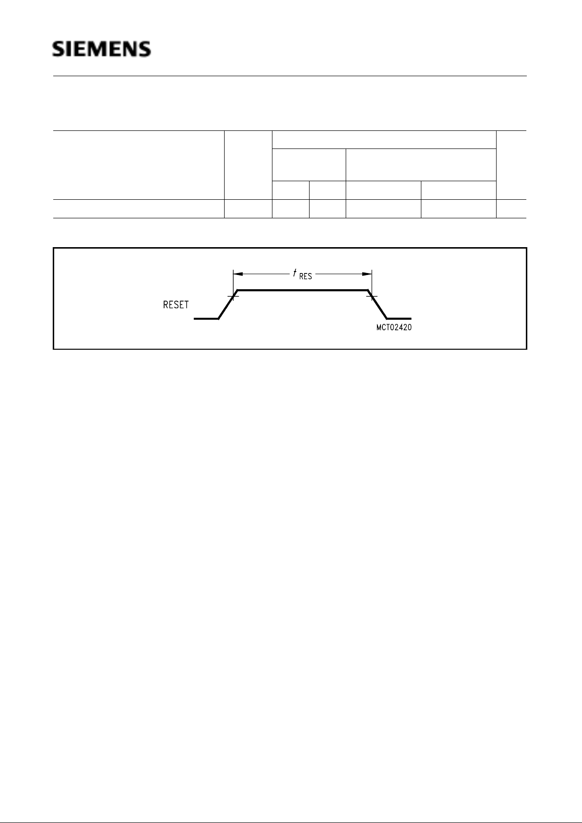
Reset Characteristics (C513A-H only)
Figure 19
C513A-H Reset Pulse
Parameter Symbol Limit Values Unit
12 MHz
Clock
Variable Clock
1/
t
CLCL
= 3.5 MHz to 12 MHz
min. max. min. max.
RESET pulse width
t
RLRH
10 – 10 – ms

C511 / C513
Semiconductor Group 43
Figure 20
AC Testing: Input, Output Waveforms
Figure 21
AC Testing: Float Waveforms
Figure 22
Recommended Oscillator Circuits for Crystal Oscillator
AC Inputs during testing are driven at VCC - 0.5 V for a logic ’1’ and 0.45 V for a logic ’0’.
Timing measurements are made at V
IHmin
for a logic ’1’ and V
ILmax
for a logic ’0’.
For timing purposes a port pin is no longer floating when a 100 mV change from load voltage
occurs and begins to float when a 100 mV change from the loaded VOH/VOL level occurs.
I
OL/IOH
≥ ± 20 mA
 Loading...