Samsung WDF710Q Users Manual

Manual for WDF710Q WiFi module
1. Introduction
WDF710Q is a Wi-Fi module compliant with IEEE802.11 b.g.n MAC/baseband/radio optimized for lowpower applications. The core chipset is from Atheros, part number QCA6006.
2. Hardware Architecture: |
|
|
|
2.1 |
Main Chipset Information |
|
|
|
Item |
Vendor |
Part Number |
|
IEEE802.11 b.g.n |
Atheros |
QCA6006 |
|
mac/baseband/radio |
|
|
2.2 |
Circuit Block Diagram |
|
|
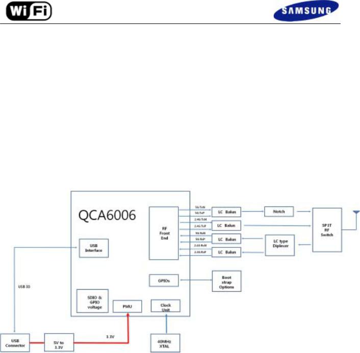
The major internal and external block diagram of WDF710Q is illustrated in Figure 1-1.
Figure 1-1 WDF710Q block diagram and System Interface
2.3 Module output power information
|
|
Data rate |
TX power |
|
||
|
|
|
|
|
|
|
|
|
2.4G |
|
5G |
|
|
|
|
|
|
|
||
|
|
|
|
|
|
|
|
802.11 b |
11Mbps |
18dBm |
|
|
|
|
|
|
|
|
|
|
|
802.11 g |
54Mbps |
14dBm |
|
10dBm |
|
|
|
|
|
|
|
|
|
802.11 n |
65Mbps (MCS7) |
13dBm |
|
8dBm |
|
|
|
|
|
|
|
|
|
|
|
|
|
|
|
Version 1.0 |
Samsung Electronics |
|
page 1 of 5 |
|||

3. Operational Description
WDF710Q is the 802.11 b/g/n RF Module that acts as a communication controller for users of a wireless device to connect to WiFi TV. This uses IEEE 802.11n network with 13 channels at 2.4GHz and 27channels at 5GHz
-Features
>IEEE 802.11n, Single stream 1x1 >Dual-band 2.4GHz /5 GHz >Integrated PA, LNA
>Green Tx power saving mode >Low power listen mode >Data rates up to 150Mbps
>Full security support : WPS,WPA,WPA2,WAPI,WEP,TKIP >Host interface : USB2.0 High-speed
-Time base of the RF frequency
For IF and RF frequency, a crystal(40MHz) is a clock reference.
- Synthesizer
Synthesizer inside Transceiver. Internal voltage controlled oscillator (VCO) provides the desired LO signal base on the phase-locked loop (PLL) with a relatively wide tuning range for this application.
- Transmission
Base-band Processing (BBP) IC has DSSS (BPSK/QPSK/CCK) and OFDM (BPSK/QPSK/16QAM/64QAM) modulation function, it provides transmission data rate are 1, 2, 5.5, 11 Mbps on DSSS and 6, 12, 18, 24, 36, 48, 54 Mbps on OFDM. Digital data signal will be converted to analog (TX IQ) signals through DAC in BBP IC, TX IQ pass through to low pass filter. TX I/Q signal use direct conversion (zero-IF) architecture converter to generate carrier frequency signal. Transceiver IC and internal PA magnify output power.
- Receiver
Reverse direction isolation of LNA inside Transceiver IC suppresses unwanted radiation. Then RF
signal will be directly down to IF signal (RX IQ) and high frequency spurious emissions are suppressed by LPF. At last RX IQ signal will be demodulated digital data.
- Power Control Level
It uses open-loop power control function to limit RF output power level using a calibration file.
- Integrated Network Processor
Network processor manages Wi-Fi link operations. The network processor code is loaded automatically from a ROM. The network processor is optimized for energy efficient communications
Version 1.0 |
Samsung Electronics |
page 2 of 5 |
 Loading...