

Page 1

Installation Instructions
Compact I/O Modules
AC Digital Modules 1769-IA8I, 1769-IA16, 1769-IM12, 1769-OA8, 1769-OA16
DC Digital Modules 1769-IG16, 1769-IQ16, 1769-IQ16F, 1769-IQ32, 1769-IQ32T, 1769-IQ6XOW4,
1769-OB8, 1769-OB16, 1769-OB16P, 1769-OB32, 1769-OB32T, 1769-OG16, 1769-OV16, 1769-OV32T
Contact Modules 1769-OW8, 1769-OW8I, 1769-OW16
Analog Modules 1769-IF4, 1769-IF4I, 1769-IF4XOF2, 1769-IF4FXOF2F, 1769-IF8, 1769-IF16C,
1769-IF16V, 1769-IR6, 1769-IT6, 1769-OF2, 1769-OF4, 1769-OF4CI, 1769-OF4VI, 1769-OF8C, 1769-OF8V
Speciality Modules 1769-ARM, 1769-ASCII, 1769-BOOLEAN, 1769-HSC
Page 2
Important User Information
IMPORTANT
Solid-state equipment has operational characteristics differing from those of electromechanical equipment. Safety
Guidelines for the Application, Installation and Maintenance of Solid State Controls (publication SGI-1.1
your local Rockwell Automation sales office or online at http://www.rockwellautomation.com/literature/
important differences between solid-state equipment and hard-wired electromechanical devices. Because of this difference,
and also because of the wide variety of uses for solid-state equipment, all persons responsible for applying this equipment
must satisfy themselves that each intended application of this equipment is acceptable.
In no event will Rockwell Automation, Inc. be responsible or liable for indirect or consequential damages resulting from
the use or application of this equipment.
The examples and diagrams in this manual are included solely for illustrative purposes. Because of the many variables and
requirements associated with any particular installation, Rockwell Automation, Inc. cannot assume responsibility or
liability for actual use based on the examples and diagrams.
No patent liability is assumed by Rockwell Automation, Inc. with respect to use of information, circuits, equipment, or
software described in this manual.
Reproduction of the contents of this manual, in whole or in part, without written permission of Rockwell Automation,
Inc., is prohibited.
Throughout this manual, when necessary, we use notes to make you aware of safety considerations.
WARNING: Identifies information about practices or circumstances that can cause an explosion in a hazardous
environment, which may lead to personal injury or death, property damage, or economic loss.
available from
) describes some
ATTENTION: Identifies information about practices or circumstances that can lead to personal injury or death,
property damage, or economic loss. Attentions help you identify a hazard, avoid a hazard, and recognize the
consequence
SHOCK HAZARD: Labels may be on or inside the equipment, for example, a drive or motor, to alert people that
dangerous voltage may be present.
BURN HAZARD: Labels may be on or inside the equipment, for example, a drive or motor, to alert people that
surfaces may reach dangerous temperatures.
Identifies information that is critical for successful application and understanding of the product.
Allen-Bradley, Compact I/O, Rockwell Automation, Rockwell Software, RS Logix 500, RSLogix 5000, R SNetWorx for DeviceNet, and TechConnect are trademarks of Rockwell Automation, Inc.
Trademarks not belonging to Rockwell Automation are property of their respective companies.
Page 3

Table of Contents
Preface
Install a 1769 Module
Module Wiring
Additional Resources . . . . . . . . . . . . . . . . . . . . . . . . . . . . . . . . . . . . . . . . . . . . . . . 9
Chapter 1
Before You Begin. . . . . . . . . . . . . . . . . . . . . . . . . . . . . . . . . . . . . . . . . . . . . . . . . 11
Hazardous Location Considerations . . . . . . . . . . . . . . . . . . . . . . . . . . . 13
Environnements Dangereux . . . . . . . . . . . . . . . . . . . . . . . . . . . . . . . . . . . 13
Install Summary. . . . . . . . . . . . . . . . . . . . . . . . . . . . . . . . . . . . . . . . . . . . . . . . . . 13
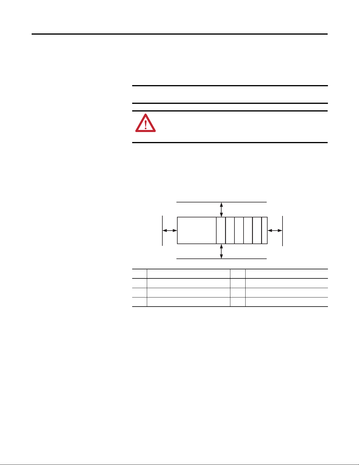
System Assembly . . . . . . . . . . . . . . . . . . . . . . . . . . . . . . . . . . . . . . . . . . . . . . . . . 14
Minimum Spacing. . . . . . . . . . . . . . . . . . . . . . . . . . . . . . . . . . . . . . . . . . . . 15
Panel Mounting . . . . . . . . . . . . . . . . . . . . . . . . . . . . . . . . . . . . . . . . . . . . . . 15
DIN Rail Mounting . . . . . . . . . . . . . . . . . . . . . . . . . . . . . . . . . . . . . . . . . . 16
Replace a Module. . . . . . . . . . . . . . . . . . . . . . . . . . . . . . . . . . . . . . . . . . . . . 17
Ground the Module . . . . . . . . . . . . . . . . . . . . . . . . . . . . . . . . . . . . . . . . . . . . . . 17
Wire the Module. . . . . . . . . . . . . . . . . . . . . . . . . . . . . . . . . . . . . . . . . . . . . . . . . 18
Label Terminals . . . . . . . . . . . . . . . . . . . . . . . . . . . . . . . . . . . . . . . . . . . . . . 18
Remove the Terminal Block . . . . . . . . . . . . . . . . . . . . . . . . . . . . . . . . . . . 19
Wire the Terminal Block. . . . . . . . . . . . . . . . . . . . . . . . . . . . . . . . . . . . . . 19
Wire Size and Terminal Screw Torque . . . . . . . . . . . . . . . . . . . . . . . . . 20
Chapter 2
1769-IA8I . . . . . . . . . . . . . . . . . . . . . . . . . . . . . . . . . . . . . . . . . . . . . . . . . . . . . . . 21
1769-IA16. . . . . . . . . . . . . . . . . . . . . . . . . . . . . . . . . . . . . . . . . . . . . . . . . . . . . . . 21
1769-IF4 . . . . . . . . . . . . . . . . . . . . . . . . . . . . . . . . . . . . . . . . . . . . . . . . . . . . . . . . 22
1769-IF4I . . . . . . . . . . . . . . . . . . . . . . . . . . . . . . . . . . . . . . . . . . . . . . . . . . . . . . . 23
1769-IF4XOF2 . . . . . . . . . . . . . . . . . . . . . . . . . . . . . . . . . . . . . . . . . . . . . . . . . . 24
1769-IF4FXOF2F . . . . . . . . . . . . . . . . . . . . . . . . . . . . . . . . . . . . . . . . . . . . . . . 25
1769-IF8 . . . . . . . . . . . . . . . . . . . . . . . . . . . . . . . . . . . . . . . . . . . . . . . . . . . . . . . . 27
1769-IF16C . . . . . . . . . . . . . . . . . . . . . . . . . . . . . . . . . . . . . . . . . . . . . . . . . . . . . 28
1769-IF16V . . . . . . . . . . . . . . . . . . . . . . . . . . . . . . . . . . . . . . . . . . . . . . . . . . . . . 29
1769-IG16 . . . . . . . . . . . . . . . . . . . . . . . . . . . . . . . . . . . . . . . . . . . . . . . . . . . . . . 29
1769-IM12 . . . . . . . . . . . . . . . . . . . . . . . . . . . . . . . . . . . . . . . . . . . . . . . . . . . . . . 30
1769-IQ16 . . . . . . . . . . . . . . . . . . . . . . . . . . . . . . . . . . . . . . . . . . . . . . . . . . . . . . 30
1769-IQ16F . . . . . . . . . . . . . . . . . . . . . . . . . . . . . . . . . . . . . . . . . . . . . . . . . . . . . 31
1769-IQ32 . . . . . . . . . . . . . . . . . . . . . . . . . . . . . . . . . . . . . . . . . . . . . . . . . . . . . . 31
1769-IQ32T. . . . . . . . . . . . . . . . . . . . . . . . . . . . . . . . . . . . . . . . . . . . . . . . . . . . . 32
1769-IQ6XOW4 . . . . . . . . . . . . . . . . . . . . . . . . . . . . . . . . . . . . . . . . . . . . . . . . 33
1769-IR6 . . . . . . . . . . . . . . . . . . . . . . . . . . . . . . . . . . . . . . . . . . . . . . . . . . . . . . . . 34
1769-IT6. . . . . . . . . . . . . . . . . . . . . . . . . . . . . . . . . . . . . . . . . . . . . . . . . . . . . . . . 36
1769-OA8. . . . . . . . . . . . . . . . . . . . . . . . . . . . . . . . . . . . . . . . . . . . . . . . . . . . . . . 36
1769-OA16 . . . . . . . . . . . . . . . . . . . . . . . . . . . . . . . . . . . . . . . . . . . . . . . . . . . . . 37
1769-OB8 . . . . . . . . . . . . . . . . . . . . . . . . . . . . . . . . . . . . . . . . . . . . . . . . . . . . . . . 37
1769-OB16. . . . . . . . . . . . . . . . . . . . . . . . . . . . . . . . . . . . . . . . . . . . . . . . . . . . . . 38
1769-OB16P . . . . . . . . . . . . . . . . . . . . . . . . . . . . . . . . . . . . . . . . . . . . . . . . . . . . 38
1769-OB32. . . . . . . . . . . . . . . . . . . . . . . . . . . . . . . . . . . . . . . . . . . . . . . . . . . . . . 39
1769-OB32T . . . . . . . . . . . . . . . . . . . . . . . . . . . . . . . . . . . . . . . . . . . . . . . . . . . . 39
Rockwell Automation Publication 1769-IN088A-EN-P - February 2011 3
Page 4

Table of Contents
1769-OF2 . . . . . . . . . . . . . . . . . . . . . . . . . . . . . . . . . . . . . . . . . . . . . . . . . . . . . . . 40
1769-OF4 . . . . . . . . . . . . . . . . . . . . . . . . . . . . . . . . . . . . . . . . . . . . . . . . . . . . . . . 40
1769-OF4CI. . . . . . . . . . . . . . . . . . . . . . . . . . . . . . . . . . . . . . . . . . . . . . . . . . . . . 41
1769-OF4VI . . . . . . . . . . . . . . . . . . . . . . . . . . . . . . . . . . . . . . . . . . . . . . . . . . . . . 41
1769-OF8C. . . . . . . . . . . . . . . . . . . . . . . . . . . . . . . . . . . . . . . . . . . . . . . . . . . . . . 42
1769-OF8V. . . . . . . . . . . . . . . . . . . . . . . . . . . . . . . . . . . . . . . . . . . . . . . . . . . . . . 43
1769-OG16. . . . . . . . . . . . . . . . . . . . . . . . . . . . . . . . . . . . . . . . . . . . . . . . . . . . . . 44
1769-OV16 . . . . . . . . . . . . . . . . . . . . . . . . . . . . . . . . . . . . . . . . . . . . . . . . . . . . . . 44
1769-OV32T . . . . . . . . . . . . . . . . . . . . . . . . . . . . . . . . . . . . . . . . . . . . . . . . . . . . 45
1769-OW8 . . . . . . . . . . . . . . . . . . . . . . . . . . . . . . . . . . . . . . . . . . . . . . . . . . . . . . 45
1769-OW8I . . . . . . . . . . . . . . . . . . . . . . . . . . . . . . . . . . . . . . . . . . . . . . . . . . . . . 46
1769-OW16 . . . . . . . . . . . . . . . . . . . . . . . . . . . . . . . . . . . . . . . . . . . . . . . . . . . . . 46
1769-ARM . . . . . . . . . . . . . . . . . . . . . . . . . . . . . . . . . . . . . . . . . . . . . . . . . . . . . . 46
1769-ASCII. . . . . . . . . . . . . . . . . . . . . . . . . . . . . . . . . . . . . . . . . . . . . . . . . . . . . . 47
1769-BOOLEAN . . . . . . . . . . . . . . . . . . . . . . . . . . . . . . . . . . . . . . . . . . . . . . . . 48
1769-HSC . . . . . . . . . . . . . . . . . . . . . . . . . . . . . . . . . . . . . . . . . . . . . . . . . . . . . . . 48
Chapter 3
I/O Memory Mapping
1769-IA8I . . . . . . . . . . . . . . . . . . . . . . . . . . . . . . . . . . . . . . . . . . . . . . . . . . . . . . . 54
Input Data File . . . . . . . . . . . . . . . . . . . . . . . . . . . . . . . . . . . . . . . . . . . . . . . 54
1769-IA16 . . . . . . . . . . . . . . . . . . . . . . . . . . . . . . . . . . . . . . . . . . . . . . . . . . . . . . . 54
Input Data File . . . . . . . . . . . . . . . . . . . . . . . . . . . . . . . . . . . . . . . . . . . . . . . 54
1769-IF4 . . . . . . . . . . . . . . . . . . . . . . . . . . . . . . . . . . . . . . . . . . . . . . . . . . . . . . . . 55
Input Data File . . . . . . . . . . . . . . . . . . . . . . . . . . . . . . . . . . . . . . . . . . . . . . . 55
Configuration Data File . . . . . . . . . . . . . . . . . . . . . . . . . . . . . . . . . . . . . . . 55
1769-IF4I. . . . . . . . . . . . . . . . . . . . . . . . . . . . . . . . . . . . . . . . . . . . . . . . . . . . . . . . 57
Input Data File . . . . . . . . . . . . . . . . . . . . . . . . . . . . . . . . . . . . . . . . . . . . . . . 57
Output Data File . . . . . . . . . . . . . . . . . . . . . . . . . . . . . . . . . . . . . . . . . . . . . 58
Configuration Data File . . . . . . . . . . . . . . . . . . . . . . . . . . . . . . . . . . . . . . . 58
1769-IF4XOF2 . . . . . . . . . . . . . . . . . . . . . . . . . . . . . . . . . . . . . . . . . . . . . . . . . . 61
Input Data File . . . . . . . . . . . . . . . . . . . . . . . . . . . . . . . . . . . . . . . . . . . . . . . 61
Output Data File . . . . . . . . . . . . . . . . . . . . . . . . . . . . . . . . . . . . . . . . . . . . . 62
Configuration Data File . . . . . . . . . . . . . . . . . . . . . . . . . . . . . . . . . . . . . . . 63
1769-IF4FXOF2F. . . . . . . . . . . . . . . . . . . . . . . . . . . . . . . . . . . . . . . . . . . . . . . . 65
Input Data File . . . . . . . . . . . . . . . . . . . . . . . . . . . . . . . . . . . . . . . . . . . . . . . 65
Output Data File . . . . . . . . . . . . . . . . . . . . . . . . . . . . . . . . . . . . . . . . . . . . . 66
Configuration Data File . . . . . . . . . . . . . . . . . . . . . . . . . . . . . . . . . . . . . . . 66
1769-IF8 . . . . . . . . . . . . . . . . . . . . . . . . . . . . . . . . . . . . . . . . . . . . . . . . . . . . . . . . 70
Input Data File . . . . . . . . . . . . . . . . . . . . . . . . . . . . . . . . . . . . . . . . . . . . . . . 70
Output Data File . . . . . . . . . . . . . . . . . . . . . . . . . . . . . . . . . . . . . . . . . . . . . 71
Configuration Data File . . . . . . . . . . . . . . . . . . . . . . . . . . . . . . . . . . . . . . . 71
Controller Tags for RSLogix 5000, Version 15 or Later . . . . . . . . . . 75
1769-IF16C . . . . . . . . . . . . . . . . . . . . . . . . . . . . . . . . . . . . . . . . . . . . . . . . . . . . . 80
Input Data File . . . . . . . . . . . . . . . . . . . . . . . . . . . . . . . . . . . . . . . . . . . . . . . 80
Output Data File . . . . . . . . . . . . . . . . . . . . . . . . . . . . . . . . . . . . . . . . . . . . . 81
4 Rockwell Automation Publication 1769-IN088A-EN-P - February 2011
Page 5

Table of Contents
Configuration Data File. . . . . . . . . . . . . . . . . . . . . . . . . . . . . . . . . . . . . . . 81
1769-IF16V . . . . . . . . . . . . . . . . . . . . . . . . . . . . . . . . . . . . . . . . . . . . . . . . . . . . . 86
Input Data File. . . . . . . . . . . . . . . . . . . . . . . . . . . . . . . . . . . . . . . . . . . . . . . 86
Output Data File . . . . . . . . . . . . . . . . . . . . . . . . . . . . . . . . . . . . . . . . . . . . . 87
Configuration Data File. . . . . . . . . . . . . . . . . . . . . . . . . . . . . . . . . . . . . . . 88
1769-IG16 . . . . . . . . . . . . . . . . . . . . . . . . . . . . . . . . . . . . . . . . . . . . . . . . . . . . . . 92
Input Data File. . . . . . . . . . . . . . . . . . . . . . . . . . . . . . . . . . . . . . . . . . . . . . . 92
Configuration File. . . . . . . . . . . . . . . . . . . . . . . . . . . . . . . . . . . . . . . . . . . . 93
1769-IM12 . . . . . . . . . . . . . . . . . . . . . . . . . . . . . . . . . . . . . . . . . . . . . . . . . . . . . . 94
Input Data File. . . . . . . . . . . . . . . . . . . . . . . . . . . . . . . . . . . . . . . . . . . . . . . 94
1769-IQ16 . . . . . . . . . . . . . . . . . . . . . . . . . . . . . . . . . . . . . . . . . . . . . . . . . . . . . . 94
Input Data File. . . . . . . . . . . . . . . . . . . . . . . . . . . . . . . . . . . . . . . . . . . . . . . 94
1769-IQ16F . . . . . . . . . . . . . . . . . . . . . . . . . . . . . . . . . . . . . . . . . . . . . . . . . . . . . 95
Input Data File. . . . . . . . . . . . . . . . . . . . . . . . . . . . . . . . . . . . . . . . . . . . . . . 95
Configuration File. . . . . . . . . . . . . . . . . . . . . . . . . . . . . . . . . . . . . . . . . . . . 95
1769-IQ32 . . . . . . . . . . . . . . . . . . . . . . . . . . . . . . . . . . . . . . . . . . . . . . . . . . . . . . 96
Input Data File. . . . . . . . . . . . . . . . . . . . . . . . . . . . . . . . . . . . . . . . . . . . . . . 96
1769-IQ32T. . . . . . . . . . . . . . . . . . . . . . . . . . . . . . . . . . . . . . . . . . . . . . . . . . . . . 96
Input Data File. . . . . . . . . . . . . . . . . . . . . . . . . . . . . . . . . . . . . . . . . . . . . . . 96
Configuration File. . . . . . . . . . . . . . . . . . . . . . . . . . . . . . . . . . . . . . . . . . . . 97
1769-IQ6XOW4 . . . . . . . . . . . . . . . . . . . . . . . . . . . . . . . . . . . . . . . . . . . . . . . . 97
Input Data File. . . . . . . . . . . . . . . . . . . . . . . . . . . . . . . . . . . . . . . . . . . . . . . 97
Output Data File . . . . . . . . . . . . . . . . . . . . . . . . . . . . . . . . . . . . . . . . . . . . . 98
Configuration File. . . . . . . . . . . . . . . . . . . . . . . . . . . . . . . . . . . . . . . . . . . . 98
1769-IR6 . . . . . . . . . . . . . . . . . . . . . . . . . . . . . . . . . . . . . . . . . . . . . . . . . . . . . . . 100
Input Data File. . . . . . . . . . . . . . . . . . . . . . . . . . . . . . . . . . . . . . . . . . . . . . 100
Configuration Data File. . . . . . . . . . . . . . . . . . . . . . . . . . . . . . . . . . . . . . 101
Module Configuration Word. . . . . . . . . . . . . . . . . . . . . . . . . . . . . . . . . 104
1769-IT6. . . . . . . . . . . . . . . . . . . . . . . . . . . . . . . . . . . . . . . . . . . . . . . . . . . . . . . 104
Input Data File. . . . . . . . . . . . . . . . . . . . . . . . . . . . . . . . . . . . . . . . . . . . . . 104
Configuration Data File. . . . . . . . . . . . . . . . . . . . . . . . . . . . . . . . . . . . . . 105
1769-OA8. . . . . . . . . . . . . . . . . . . . . . . . . . . . . . . . . . . . . . . . . . . . . . . . . . . . . . 107
Output Module’s Input Data File . . . . . . . . . . . . . . . . . . . . . . . . . . . . . 107
Output Data File . . . . . . . . . . . . . . . . . . . . . . . . . . . . . . . . . . . . . . . . . . . . 108
Configuration File. . . . . . . . . . . . . . . . . . . . . . . . . . . . . . . . . . . . . . . . . . . 108
1769-OA16 . . . . . . . . . . . . . . . . . . . . . . . . . . . . . . . . . . . . . . . . . . . . . . . . . . . . 110
Output Module’s Input Data File . . . . . . . . . . . . . . . . . . . . . . . . . . . . . 110
Output Data File . . . . . . . . . . . . . . . . . . . . . . . . . . . . . . . . . . . . . . . . . . . . 111
Configuration File. . . . . . . . . . . . . . . . . . . . . . . . . . . . . . . . . . . . . . . . . . . 111
1769-OB8, Series A . . . . . . . . . . . . . . . . . . . . . . . . . . . . . . . . . . . . . . . . . . . . . 113
Output Module’s Input Data File . . . . . . . . . . . . . . . . . . . . . . . . . . . . . 113
Output Data File . . . . . . . . . . . . . . . . . . . . . . . . . . . . . . . . . . . . . . . . . . . . 114
Configuration File. . . . . . . . . . . . . . . . . . . . . . . . . . . . . . . . . . . . . . . . . . . 114
1769-OB16, Series B . . . . . . . . . . . . . . . . . . . . . . . . . . . . . . . . . . . . . . . . . . . . 116
Output Module’s Input Data File . . . . . . . . . . . . . . . . . . . . . . . . . . . . . 116
Output Data File . . . . . . . . . . . . . . . . . . . . . . . . . . . . . . . . . . . . . . . . . . . . 117
Rockwell Automation Publication 1769-IN088A-EN-P - February 2011 5
Page 6

Table of Contents
Configuration File . . . . . . . . . . . . . . . . . . . . . . . . . . . . . . . . . . . . . . . . . . . 117
1769-OB16P. . . . . . . . . . . . . . . . . . . . . . . . . . . . . . . . . . . . . . . . . . . . . . . . . . . . 119
Output Module’s Input Data File . . . . . . . . . . . . . . . . . . . . . . . . . . . . . 119
Output Data File . . . . . . . . . . . . . . . . . . . . . . . . . . . . . . . . . . . . . . . . . . . . 120
Configuration File . . . . . . . . . . . . . . . . . . . . . . . . . . . . . . . . . . . . . . . . . . . 120
1769-OB32 . . . . . . . . . . . . . . . . . . . . . . . . . . . . . . . . . . . . . . . . . . . . . . . . . . . . . 122
Output Module’s Input Data File . . . . . . . . . . . . . . . . . . . . . . . . . . . . . 122
Output Data File . . . . . . . . . . . . . . . . . . . . . . . . . . . . . . . . . . . . . . . . . . . . 123
Configuration File . . . . . . . . . . . . . . . . . . . . . . . . . . . . . . . . . . . . . . . . . . . 123
1769-OB32T . . . . . . . . . . . . . . . . . . . . . . . . . . . . . . . . . . . . . . . . . . . . . . . . . . . 125
Input Data File . . . . . . . . . . . . . . . . . . . . . . . . . . . . . . . . . . . . . . . . . . . . . . 125
Output Data File . . . . . . . . . . . . . . . . . . . . . . . . . . . . . . . . . . . . . . . . . . . . 126
Configuration File . . . . . . . . . . . . . . . . . . . . . . . . . . . . . . . . . . . . . . . . . . . 126
1769-OF2 . . . . . . . . . . . . . . . . . . . . . . . . . . . . . . . . . . . . . . . . . . . . . . . . . . . . . . 128
Input Data File . . . . . . . . . . . . . . . . . . . . . . . . . . . . . . . . . . . . . . . . . . . . . . 128
Output Data File . . . . . . . . . . . . . . . . . . . . . . . . . . . . . . . . . . . . . . . . . . . . 129
Configuration Data File . . . . . . . . . . . . . . . . . . . . . . . . . . . . . . . . . . . . . . 130
1769-OF4 . . . . . . . . . . . . . . . . . . . . . . . . . . . . . . . . . . . . . . . . . . . . . . . . . . . . . . 132
Input Data File . . . . . . . . . . . . . . . . . . . . . . . . . . . . . . . . . . . . . . . . . . . . . . 132
Output Data File . . . . . . . . . . . . . . . . . . . . . . . . . . . . . . . . . . . . . . . . . . . . 132
Configuration Data File . . . . . . . . . . . . . . . . . . . . . . . . . . . . . . . . . . . . . . 133
1769-OF4CI. . . . . . . . . . . . . . . . . . . . . . . . . . . . . . . . . . . . . . . . . . . . . . . . . . . . 135
Input Data File . . . . . . . . . . . . . . . . . . . . . . . . . . . . . . . . . . . . . . . . . . . . . . 135
Output Data File . . . . . . . . . . . . . . . . . . . . . . . . . . . . . . . . . . . . . . . . . . . . 136
Configuration Data File . . . . . . . . . . . . . . . . . . . . . . . . . . . . . . . . . . . . . . 136
1769-OF4VI . . . . . . . . . . . . . . . . . . . . . . . . . . . . . . . . . . . . . . . . . . . . . . . . . . . . 139
Input Data File . . . . . . . . . . . . . . . . . . . . . . . . . . . . . . . . . . . . . . . . . . . . . . 139
Output Data File . . . . . . . . . . . . . . . . . . . . . . . . . . . . . . . . . . . . . . . . . . . . 139
Configuration Data File . . . . . . . . . . . . . . . . . . . . . . . . . . . . . . . . . . . . . . 140
1769-OF8C. . . . . . . . . . . . . . . . . . . . . . . . . . . . . . . . . . . . . . . . . . . . . . . . . . . . . 142
Input Data File . . . . . . . . . . . . . . . . . . . . . . . . . . . . . . . . . . . . . . . . . . . . . . 142
Output Data File . . . . . . . . . . . . . . . . . . . . . . . . . . . . . . . . . . . . . . . . . . . . 143
Configuration Data File . . . . . . . . . . . . . . . . . . . . . . . . . . . . . . . . . . . . . . 144
Controller Tags for RSLogix 5000, Version 15 or Later
. . . . . . . . . 146
1769-OF8V. . . . . . . . . . . . . . . . . . . . . . . . . . . . . . . . . . . . . . . . . . . . . . . . . . . . . 152
Input Data File . . . . . . . . . . . . . . . . . . . . . . . . . . . . . . . . . . . . . . . . . . . . . . 152
Output Data File . . . . . . . . . . . . . . . . . . . . . . . . . . . . . . . . . . . . . . . . . . . . 153
Configuration Data File . . . . . . . . . . . . . . . . . . . . . . . . . . . . . . . . . . . . . . 153
Controller Tags for RSLogix 5000, Version 15 or Later . . . . . . . . . 157
Output Data . . . . . . . . . . . . . . . . . . . . . . . . . . . . . . . . . . . . . . . . . . . . . . . . 161
1769-OG16. . . . . . . . . . . . . . . . . . . . . . . . . . . . . . . . . . . . . . . . . . . . . . . . . . . . . 162
Output Module’s Input Data File . . . . . . . . . . . . . . . . . . . . . . . . . . . . . 162
Output Data File . . . . . . . . . . . . . . . . . . . . . . . . . . . . . . . . . . . . . . . . . . . . 162
Configuration File . . . . . . . . . . . . . . . . . . . . . . . . . . . . . . . . . . . . . . . . . . . 163
1769-OV16 . . . . . . . . . . . . . . . . . . . . . . . . . . . . . . . . . . . . . . . . . . . . . . . . . . . . . 165
Output Module’s Input Data File . . . . . . . . . . . . . . . . . . . . . . . . . . . . . 165
6 Rockwell Automation Publication 1769-IN088A-EN-P - February 2011
Page 7

Table of Contents
Output Data File . . . . . . . . . . . . . . . . . . . . . . . . . . . . . . . . . . . . . . . . . . . . 165
Configuration File. . . . . . . . . . . . . . . . . . . . . . . . . . . . . . . . . . . . . . . . . . . 166
1769-OV32T . . . . . . . . . . . . . . . . . . . . . . . . . . . . . . . . . . . . . . . . . . . . . . . . . . . 167
Output Module’s Input Data File . . . . . . . . . . . . . . . . . . . . . . . . . . . . . 167
Output Data File . . . . . . . . . . . . . . . . . . . . . . . . . . . . . . . . . . . . . . . . . . . . 168
Configuration File. . . . . . . . . . . . . . . . . . . . . . . . . . . . . . . . . . . . . . . . . . . 168
1769-OW8 . . . . . . . . . . . . . . . . . . . . . . . . . . . . . . . . . . . . . . . . . . . . . . . . . . . . . 170
Output Module’s Input Data File . . . . . . . . . . . . . . . . . . . . . . . . . . . . . 170
Output Data File . . . . . . . . . . . . . . . . . . . . . . . . . . . . . . . . . . . . . . . . . . . . 171
Configuration File. . . . . . . . . . . . . . . . . . . . . . . . . . . . . . . . . . . . . . . . . . . 171
1769-OW8I . . . . . . . . . . . . . . . . . . . . . . . . . . . . . . . . . . . . . . . . . . . . . . . . . . . . 173
Output Module’s Input Data File . . . . . . . . . . . . . . . . . . . . . . . . . . . . . 173
Output Data File . . . . . . . . . . . . . . . . . . . . . . . . . . . . . . . . . . . . . . . . . . . . 174
Configuration File. . . . . . . . . . . . . . . . . . . . . . . . . . . . . . . . . . . . . . . . . . . 174
1769-OW16. . . . . . . . . . . . . . . . . . . . . . . . . . . . . . . . . . . . . . . . . . . . . . . . . . . . 176
Output Module’s Input Data File . . . . . . . . . . . . . . . . . . . . . . . . . . . . . 176
Output Data File . . . . . . . . . . . . . . . . . . . . . . . . . . . . . . . . . . . . . . . . . . . . 177
Configuration File. . . . . . . . . . . . . . . . . . . . . . . . . . . . . . . . . . . . . . . . . . . 177
1769-ARM . . . . . . . . . . . . . . . . . . . . . . . . . . . . . . . . . . . . . . . . . . . . . . . . . . . . . 179
Input Data File. . . . . . . . . . . . . . . . . . . . . . . . . . . . . . . . . . . . . . . . . . . . . . 179
1769-ASCII . . . . . . . . . . . . . . . . . . . . . . . . . . . . . . . . . . . . . . . . . . . . . . . . . . . . 180
Alternate Mode (One Channel at a Time) Input File . . . . . . . . . . . 180
Alternate Mode (One Channel at a Time) Output File . . . . . . . . . 181
Simultaneous Mode (Two Channels) Input File . . . . . . . . . . . . . . . 182
Simultaneous Mode (Two Channels) Output File. . . . . . . . . . . . . . 184
Configuration File. . . . . . . . . . . . . . . . . . . . . . . . . . . . . . . . . . . . . . . . . . . 185
1769-BOOLEAN. . . . . . . . . . . . . . . . . . . . . . . . . . . . . . . . . . . . . . . . . . . . . . . 187
Input Data File. . . . . . . . . . . . . . . . . . . . . . . . . . . . . . . . . . . . . . . . . . . . . . 187
Output Data File . . . . . . . . . . . . . . . . . . . . . . . . . . . . . . . . . . . . . . . . . . . . 187
Configuration Data File. . . . . . . . . . . . . . . . . . . . . . . . . . . . . . . . . . . . . . 188
1769-HSC . . . . . . . . . . . . . . . . . . . . . . . . . . . . . . . . . . . . . . . . . . . . . . . . . . . . . 195
Module Replacement Parts
Rockwell Automation Publication 1769-IN088A-EN-P - February 2011 7
Appendix A
. . . . . . . . . . . . . . . . . . . . . . . . . . . . . . . . . . . . . . . . . . . . . . . . . . . . . . . . . . . . . . . . 197
Page 8

Table of Contents
Notes:
8 Rockwell Automation Publication 1769-IN088A-EN-P - February 2011
Page 9

Preface
This manual describes how to install any 1769 Compact I/O module. Use this
manual if you are responsible for designing, installing, programming, or
troubleshooting control systems that use Compact I/O modules.
Additional Resources
These documents contain additional information concerning related Rockwell
Automation products.
Resource Description
Industrial Automation Wiring and Grounding
Guidelines, publication 1770-4.1
Product Certifications website,
http://www.ab.com
Compact I/O Thermocouple/mV Input Module
User Manual, publication 1769-UM004
Compact I/O RTD/Resistance Input Module User
Manual, publication 1769-UM005
Compact High-speed Counter Module User
Manual, publication 1769-UM006
Compact 8-Bit Low Resolution Analog I/O
Combination Module User Manual, publication
1769-UM008
Compact I/O ASCII Module User Manual,
publication 1769-UM012
Compact I/O Isolated Analog Modules User
Manual, publication 1769-UM014
Compact I/O BOOLEAN Module User Manual,
publication 1769-UM016
Compact High Density Analog Input Modules
User Manual, publication 1769-UM018
Compact Combination Fast Analog I/O Module
User Manual, publication 1769-UM019
Compact Analog Output Module User Manual,
publication 1769-UM020
Provides general guidelines for installing a
Rockwell Automation industrial system.
Provides declarations of conformity, certificates,
and other certification details.
Provides a quick start and describes how to
install, configure, and troubleshoot the
CompactI/O Thermocouple/mV Input module.
Describes how to install, configure, program,
operate, and troubleshoot a control system using
the 1769-IR6 module.
Describes how to operate, install, wire,
configure, and troubleshoot the 1769-HSC
module.
Provides a quick start and describes how to
install, configure, program, operate, and
troubleshoot a control system using the 1769
combination analog I/O module.
Provides a quick start and describes how to
install, configure, and troubleshoot the
Compact I/O 1769-ASCII module.
Describes how to install, configure, program,
operate, and troubleshoot a control system using
1769 isolated analog I/O modules.
Describes how to install, configure, program,
operate, and troubleshoot a control system using
the 1769 BOOLEAN module.
Describes how to install, configure, and
troubleshoot 1769 compact high density analog
input modules.
Describes how to install, configure, and
troubleshoot the 1769 combination analog I/O
module.
Describes how to install, configure, and
troubleshoot the 1769 analog I/O module.
You can view or download publications at http://www.rockwellautomation.com/
literature/. To order paper copies of technical documentation, contact your local
Rockwell Automation distributor or sales representative.
Rockwell Automation Publication 1769-IN088A-EN-P - February 2011 9
Page 10

Preface
Notes:
10 Rockwell Automation Publication 1769-IN088A-EN-P - February 2011
Page 11
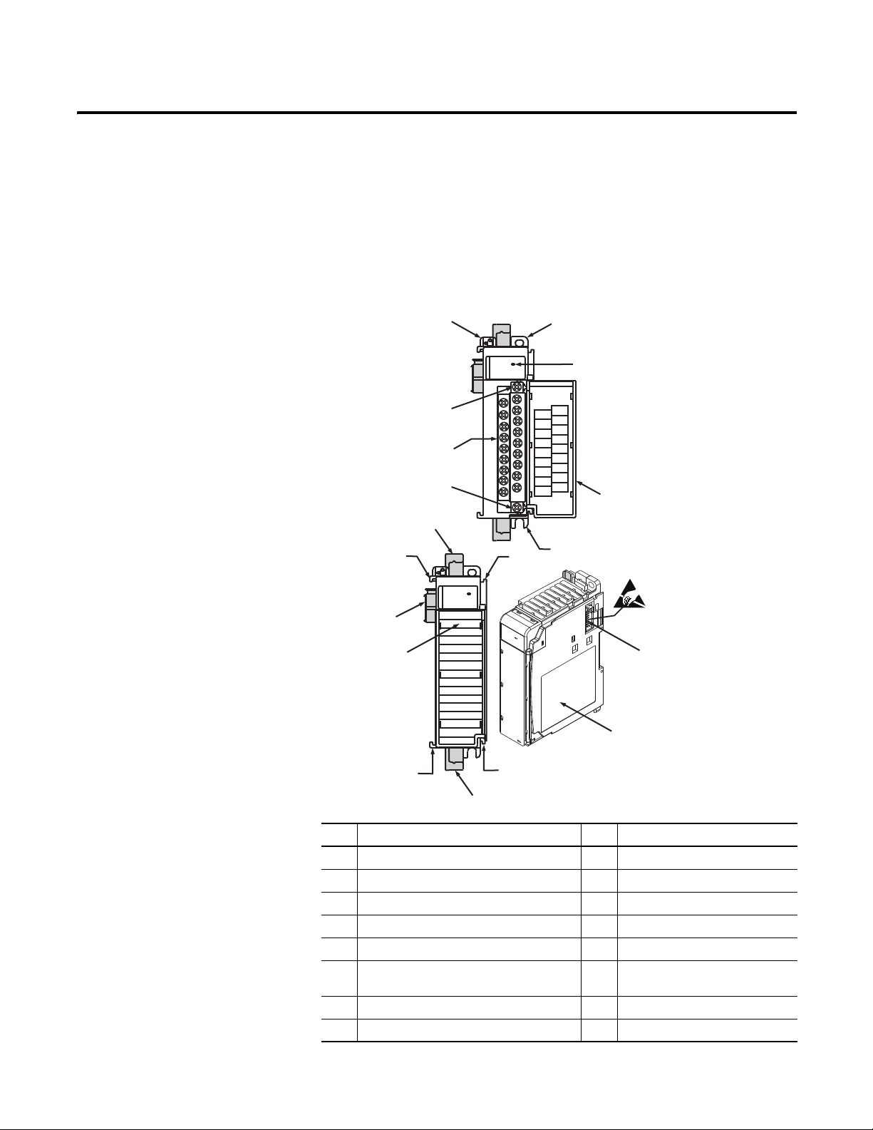
Install a 1769 Module
10a
10b
4
10
2b
3
2a
1
5a
9
5b
6
7a
7b
8b
7b
8a
7a
1769-OF4VI
DANGER
Do Not Remove RTB Under Power
Unless Area is Non-Hazardous
Ensure Adjacent
Bus Lever is Unlatched/Latched
Before/After
Removing/Inserting Module
N/C
V out 1 +
N/C
V out 2 +
N/C
V out 3 +
N/C
V out 0 +
N/C
N/C
V out 1 -
N/C
V out 2 -
N/C
V out 3 -
N/C
V out 0 -
N/C
OK
Analog
OK
Analog
Chapter
1
Before You Begin
Compact I/O is suitable for use in an industrial environment when installed in
accordance with these instructions.
Item Description Item Description
1 Bus lever (with locking function) 7a Upper tongue-and-groove slots
2a Upper panel mounting tab 7b Lower tongue-and-groove slots
2b Lower panel mounting tab 8a Upper DIN rail latch
3 Module status LED 8b Lower DIN rail latch
4 Module door with terminal identification label 9 Write-on label (user ID tag)
5a Movable bus connector with female pins 10 Removable terminal block (RTB)
with finger-safe cover
5b Stationary bus connector with male pins 10a RTB upper retaining screw
6 Nameplate label 10b RTB lower retaining screw
Rockwell Automation Publication 1769-IN088A-EN-P - February 2011 11
Page 12
Chapter 1 Install a 1769 Module
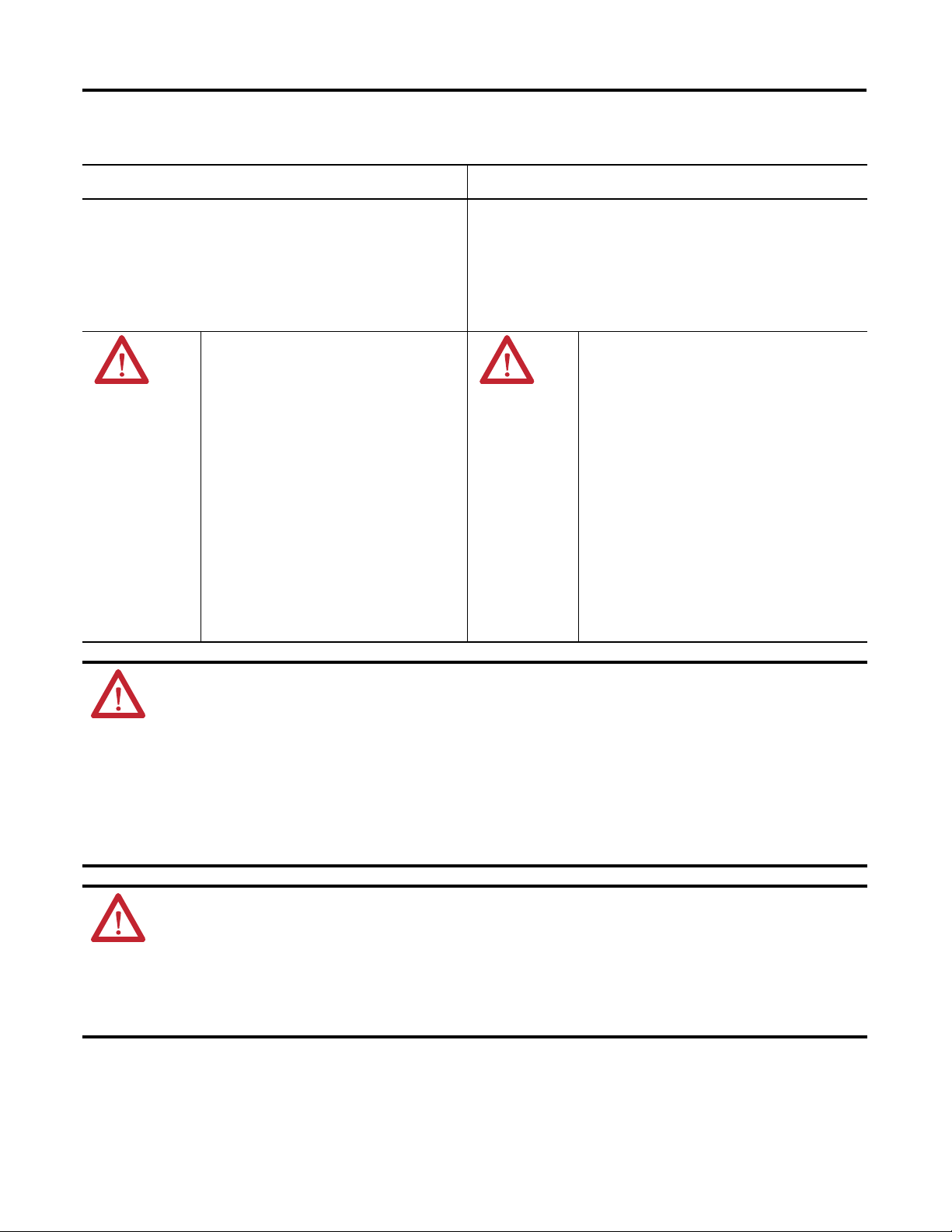
North American Hazardous Location Approval
The following information applies when operating this equipment
in hazardous locations.
Products marked "CL I, DIV 2, GP A, B, C, D" are suitable for use in Class I
Division 2 Groups A, B, C, D, Hazardous Locations and nonhazardous
locations only. Each product is supplied with markings on the rating
nameplate indicating the hazardous location temperature code. When
combining products within a system, the most adverse temperature code
(lowest "T" number) may be used to help determine the overall temperature
code of the system. Combinations of equipment in your system are subject
to investigation by the local Authority Having Jurisdiction at the time of
installation.
WARNING:
Explosion Hazard
• Do not disconnect equipment unless
power has been removed or the area is
known to be nonhazardous.
• Do not disconnect connections to this
equipment unless power has been
removed or the area is known to be
nonhazardous. Secure any external
connections that mate to this
equipment by using screws, sliding
latches, threaded connectors, or other
means provided with this product.
• Substitution of components may impair
suitability for Class I, Division 2.
• If this product contains batteries, they
must only be changed in an area known
to be nonhazardous.
Informations sur l’utilisation de cet équipement en environnements
dangereux.
Les produits marqués "CL I, DIV 2, GP A, B, C, D" ne conviennent qu'à une
utilisation en environnements de Classe I Division 2 Groupes A, B, C, D
dangereux et non dangereux. Chaque produit est livré avec des marquages sur
sa plaque d'identification qui indiquent le code de température pour les
environnements dangereux. Lorsque plusieurs produits sont combinés dans un
système, le code de température le plus défavorable (code de température le
plus faible) peut être utilisé pour déterminer le code de température global du
système. Les combinaisons d'équipements dans le système sont sujettes à
inspection par les autorités locales qualifiées au moment de l'installation.
AVERTISSEMENT:
Risque d’Explosion
• Couper le courant ou s'assurer que
l'environnement est classé non dangereux
avant de débrancher l'équipement.
• Couper le courant ou s'assurer que
l'environnement est classé non dangereux
avant de débrancher les connecteurs. Fixer
tous les connecteurs externes reliés à cet
équipement à l'aide de vis, loquets
coulissants, connecteurs filetés ou autres
moyens fournis avec ce produit.
• La substitution de composants peut rendre
cet équipement inadapté à une utilisation
en environnement de Classe I, Division 2.
• S'assurer que l'environnement est classé
non dangereux avant de changer les piles.
ATTENTION: Prevent Electrostatic Discharge
Electrostatic discharge can damage integrated circuits or semiconductors if you touch bus connector pins or the
terminal block. Follow these guidelines when you handle the module:
• Touch a grounded object to discharge static potential.
• Wear an approved wrist-strap grounding device.
• Do not touch the bus connector or connector pins.
• Do not touch circuit components inside the module.
• Use a static-safe work station, if available.
• When not in use, keep the module in its static-shield box.
ATTENTION: Remove power before removing or inserting this module. When you remove or insert a module with
power applied, an electrical arc may occur. An electrical arc can cause personal injury or property damage in these
ways:
• Sending an erroneous signal to your system’s field devices causing unintended machine motion
• Causing an explosion in a hazardous environment
Electrical arcing causes excessive wear to contacts on both the module and its mating connector. Worn contacts may
create electrical resistance.
12 Rockwell Automation Publication 1769-IN088A-EN-P - February 2011
Page 13

Install a 1769 Module Chapter 1
Hazardous Location Considerations
This equipment is suitable for use in Class I, Division 2, Groups A, B, C, D or
non-hazardous locations only. The following WARNING statement applies to
use in hazardous locations.
WARNING: EXPLOSION HAZARD
• Substitution of components may impair suitability for Class I, Division 2.
• When in hazardous locations, turn off power before wiring or replacing
modules.
• Do not disconnect equipment unless power has been switched off or the
area is known to be non-hazardous.
• This product must be installed in an enclosure.
• All wiring must comply with N.E.C. article 501-4(b).
Environnements Dangereux
Install Summary
Cet équipement est conçu pour être utilisé dans des environnements de Classe 1,
Division 2, Groupes A, B, C, D ou non dangereux. La mise en garde suivante
s’applique à une utilisation dans des environnements dangereux.
WARNING: DANGER D’EXPLOSION
La substitution de composants peut rendre cet équipement impropre à une
utilisation en environnement de Classe 1, Division 2.
Ne pas remplacer de composants ou déconnecter l'équipement sans s'être
assuré que l'alimentation est coupée et que l'environnement est classé non
dangereux.
Ne pas connecter ou déconnecter des composants sans s'être assuré que
l'alimentation est coupée ou que l'environnement est classé non dangereux.
Ce produit doit être installé dans une armoire.
Follow these steps to install the module.
1. System Assembly
2. Ground the Module
3. Wire the Module
.
.
.
This publication describes these steps in detail.
Rockwell Automation Publication 1769-IN088A-EN-P - February 2011 13
Page 14
Chapter 1 Install a 1769 Module
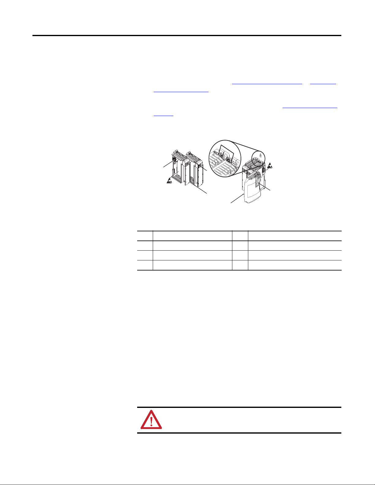
System Assembly
The module can be attached to the controller or an adjacent I/O module before
or after mounting.
• For mounting instructions, see Panel Mounting
on page 15 or DIN Rail
Mounting on page 16.
• To work with a system that is already mounted, see Replace a Module
on
page 17.
The following procedure shows you how to assemble the Compact I/O system.
3
4
2
Item Description Item Description
1 Tongue-and-groove slots 4 Bus lever
2 Bus connectors 5 End-cap terminator
3 Positioning tab 6 End-cap bus terminator
1
1
5
6
1. Disconnect power.
2. Check that the bus lever of the module to be installed is in the unlocked
(fully right) position.
3. Use the upper and lower tongue-and-groove slots (1) to secure the modules
together (or to a controller).
4. Move the module back along the tongue-and-groove slots until the bus
connectors (2) line up with each other.
5. Push the bus lever back slightly to clear the positioning tab (3).
Use your fingers or a small screwdriver.
6. To allow communication between the controller and module, move the
bus lever fully to the left (4) until it clicks.
7. Make sure the lever is locked firmly in place.
ATTENTION: When attaching I/O modules, it is very important that the
bus connectors are securely locked together to make a proper electrical
connection.
14 Rockwell Automation Publication 1769-IN088A-EN-P - February 2011
Page 15
Install a 1769 Module Chapter 1
IMPORTANT
1
5
4
4
6
2
2
2
2
2
3
8. Attach an end-cap terminator (5) to the last module in the system by using
the tongue-and-groove slots as before.
9. Lock the end-cap bus terminator (6).
A 1769-ECR or 1769-ECL right or left end cap must be used to terminate
the end of the serial communication bus.
ATTENTION: During panel or DIN rail mounting of all devices, be sure
that all debris, such as metal chips and wire strands, is kept from falling
into the module. Debris that falls into the module could cause damage on
powerup.
Minimum Spacing
Maintain spacing from enclosure walls, wireways, and adjacent equipment. Allow
50 mm (2 in.) of space on all sides for adequate ventilation.
Item Description Item Description
1Top 4Side
2 Compact I/O modules 5 Bottom
3 End cap 6 Host controller
Panel Mounting
Mount the module to a panel by using two screws per module. Use M4 or #8
panhead screws. Mounting screws are required on every module.
Rockwell Automation Publication 1769-IN088A-EN-P - February 2011 15
Page 16
Chapter 1 Install a 1769 Module
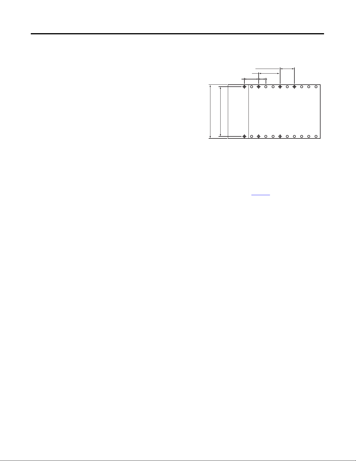
Spacing for single-wide modules 35mm (1.378 in.)
Spacing for one-and-a half-wide modules 52.5mm (2.067 in.)
Refer to host controller documentation for this dimension.
Host Controller
Note: Overall hole spacing
tolerance: ±0.4mm (0.016 in.).
30535-M
Host Controller
Note: Overall hole spacing
tolerance: +/- 0.4mm (0.016 in.).
Spacing for one-and-a half-wide modules 52.5mm (2.067 in.)
Refer to host controller documentation for this dimension.
Spacing for single-wide modules 35mm (1.378 in.)
TIP
Panel Mounting Using the Dimensional Template
Panel Mounting Procedure Using Modules as a Template
The following procedure lets you use the assembled modules as a template for
drilling holes in the panel. If you have sophisticated panel mounting equipment,
you can use the dimensional template provided on page 16
mounting hole tolerance, it is important to follow these procedures.
. Due to module
1. On a clean work surface, assemble no more than three modules.
2. Using the assembled modules as a template, carefully mark the center of all
module-mounting holes on the panel.
3. Return the assembled modules to the clean work surface, including any
previously mounted modules.
4. Drill and tap the mounting holes for the recommended M4 or #8 screw.
5. Place the modules back on the panel, and check for proper hole alignment.
6. Attach the modules to the panel using the mounting screws.
If you are mounting more modules, mount only the last one of this group
and put the others aside. This reduces remounting time during drilling
and tapping of the next group.
7. Repeat steps 1…6 for any remaining modules.
DIN Rail Mounting
The module can be mounted using the following DIN rails:
• 35 x 7.5 mm (1.38 x 0.30 in.; EN 50 022 - 35 x 7.5)
• 35 x 15 mm (1.38 x 0.59 in.; EN 50 022 - 35 x 15)
16 Rockwell Automation Publication 1769-IN088A-EN-P - February 2011
Before mounting the module on a DIN rail, close the DIN rail latches. Press the
DIN rail mounting area of the module against the DIN rail. The latches will
momentarily open and lock into place.
Page 17

Install a 1769 Module Chapter 1
TIP
Replace a Module
To replace the module while the system is mounted to a panel or DIN rail, follow
these steps.
1. Remove power.
2. On the module to be removed, use a screwdriver to remove the upper and
lower mounting screws from the module or open the DIN latches.
3. Move the bus lever to the right to disconnect or unlock the bus.
4. On the right-side adjacent module, move its bus lever to the right to
disconnect it from the module to be removed.
5. Gently slide the disconnected module forward.
If you feel excessive resistance, check that the module has been
disconnected from the bus, and that both mounting screws have been
removed or DIN latches have been opened.
It may be necessary to rock the module slightly from front to back to
remove it, or, in a panel-mounted system, to loosen the screws of
adjacent modules.
Ground the Module
6. Before installing the replacement module, be sure that the bus lever on the
module to be installed and the bus lever on the right-side adjacent module
are in the unlocked (fully right) position.
7. Slide the replacement module into the open slot.
8. Connect the modules together by locking (fully left) the bus levers on the
replacement module and the right-side adjacent module.
9. Replace the mounting screws or snap the module onto the DIN rail.
This product is intended to be mounted to a well-grounded mounting surface,
such as a metal panel. Additional grounding connections from the module’s
mounting tabs or DIN rail are not required unless the mounting surface cannot
be grounded. Refer to the Industrial Automation Wiring and Grounding
Guidelines, publication 1770-4.1
, for additional information.
Rockwell Automation Publication 1769-IN088A-EN-P - February 2011 17
Page 18

Chapter 1 Install a 1769 Module
TIP
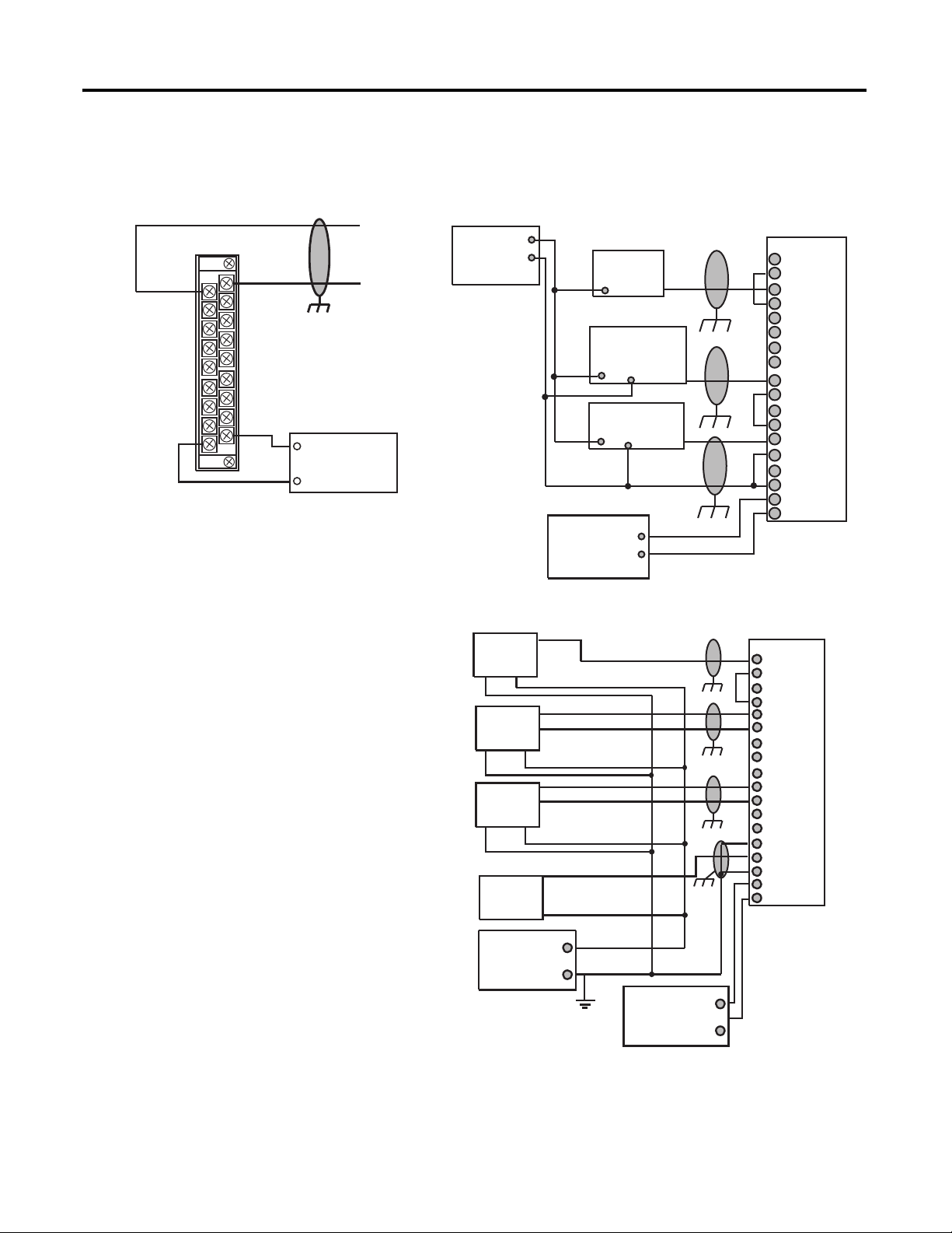
Wire the Module
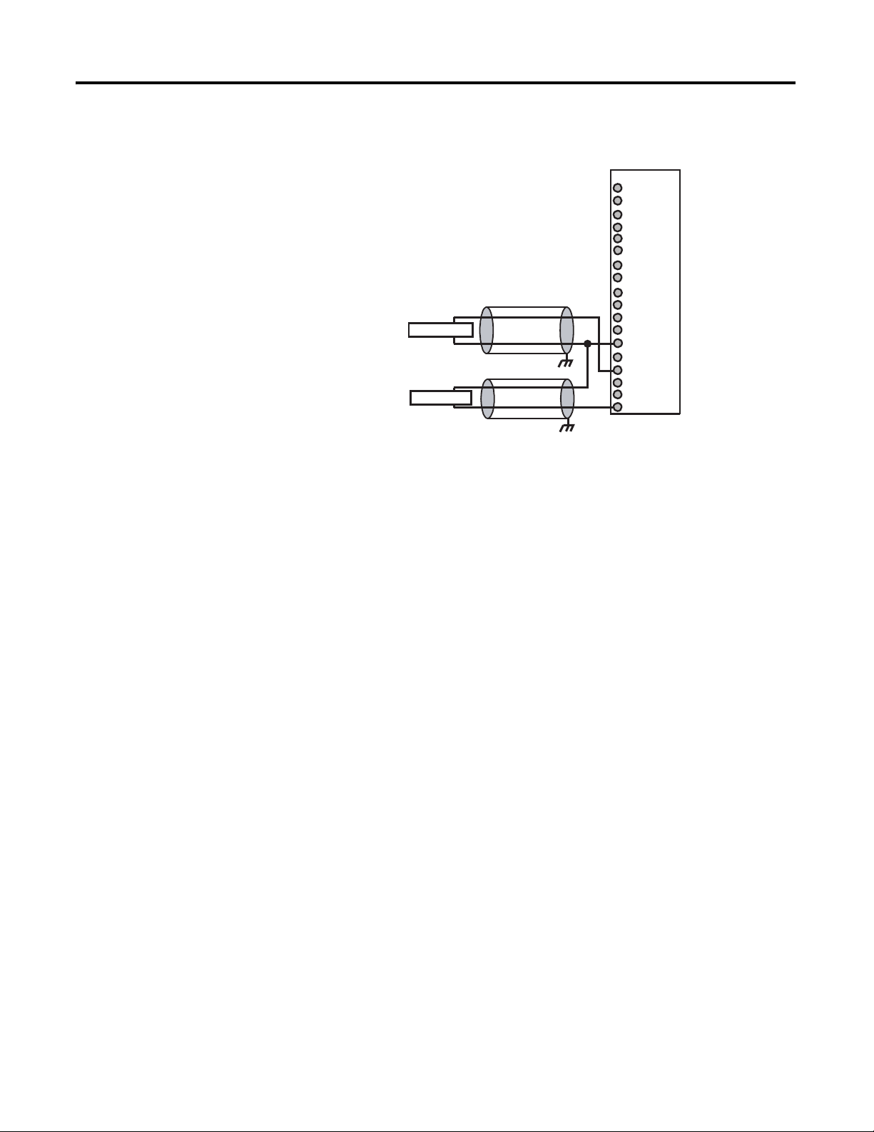
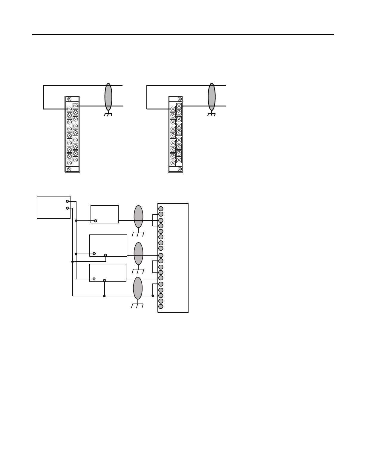
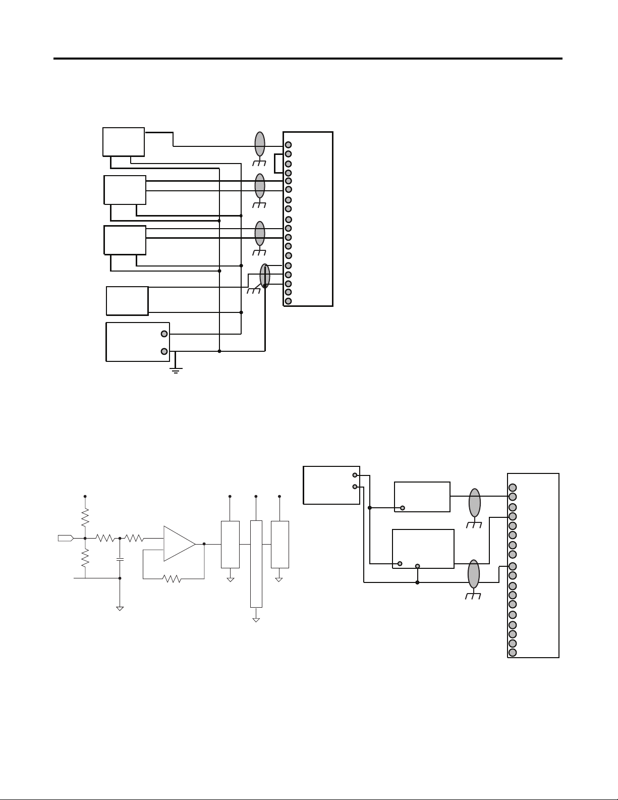
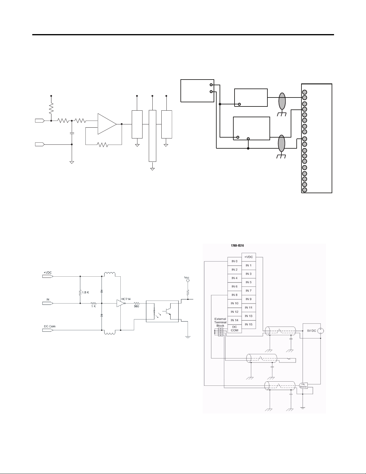
Consider the following when wiring your system:
• Channels are isolated from each other.
• Use Belden 8761, or equivalent, shielded wire.
• Under normal conditions, the drain wire and shield junction must be
connected to earth ground with a panel or DIN rail mounting screw at the
analog I/O module end. Keep the shield connection to ground as short as
possible.
In environments where high frequency noise may be present, it may be
necessary to ground the shield via a 0.1 µF capacitor at the load end and
also ground the module end without a capacitor.
• For optimum accuracy, limit overall cable impedance by keeping your cable
as short as possible. Locate the I/O system as close to your sensors or
actuators as your application will permit.
• Load resistance for each voltage output channel must be equal to or greater
than 2K
Ω..
ATTENTION: Miswiring of the module to an AC/DC source will damage
the module.
Be careful when stripping wires. Wire fragments that fall into a module
could cause damage at powerup. Once wiring is complete, make sure the
module is free of all metal fragments.
Refer to Appendix 2
for wiring diagrams of each module.
Label Terminals
A removable, write-on label is provided with the module. Remove the label from
the door, mark the identification of each terminal with permanent ink, and slide
the label back into the door. Your markings (ID tag) will be visible when the
module door is closed.
18 Rockwell Automation Publication 1769-IN088A-EN-P - February 2011
Page 19
Install a 1769 Module Chapter 1
TIP
TIP
1
3
2
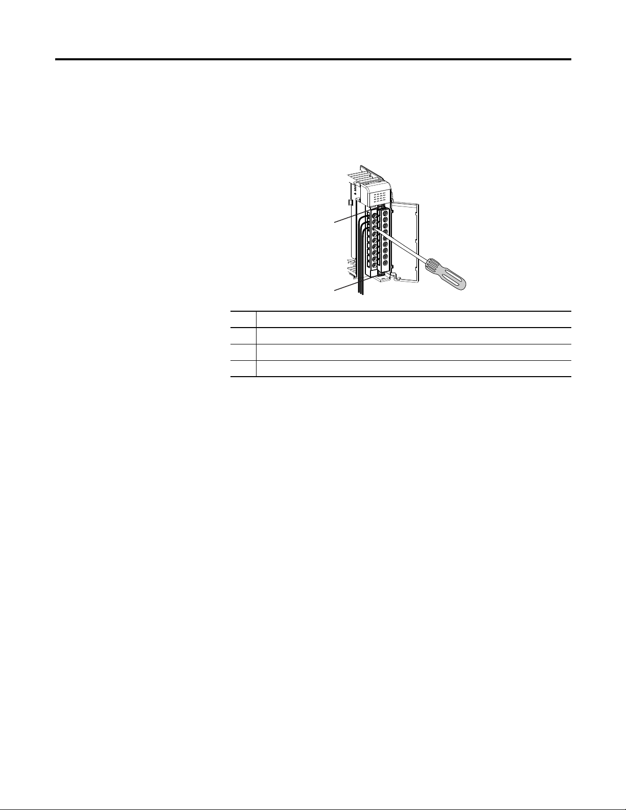
Remove the Terminal Block
To remove the terminal block, loosen the upper and lower retaining screws. The
terminal block will back away from the module as you remove the screws. When
replacing the terminal block, torque the retaining screws to 0.46 N
Item Description
1 Wiring the finger-safe terminal block
2 Lower retaining screws
3 Upper retaining screws
•m (4.1 lb•in).
Wire the Terminal Block
When wiring the terminal block, keep the finger-safe cover in place.
1. Loosen the terminal screws to be wired.
2. Route the wire under the terminal pressure plate.
You can use the bare wire or a spade lug. The terminals will accept a 6.35
mm (0.25 in.) spade lug.
The terminal screws are non-captive. You can use a ring lug [maximum
6.35 mm (0.25 in.) o.d. with a 3.53 mm (0.139 in.) minimum i.d. (M3.5)]
with the module.
3. Tighten the terminal screw making sure the pressure plate secures the wire.
Recommended torque when tightening terminal screws is 0.68 N•m
(6 lb•in).
If you need to remove the finger-safe cover, insert a screwdriver into one
of the square wiring holes and gently pry the cover off. If you wire the
terminal block with the finger-safe cover removed, you will not be able to
put it back on the terminal block because the wires will be in the way.
Rockwell Automation Publication 1769-IN088A-EN-P - February 2011 19
Page 20

Chapter 1 Install a 1769 Module
Wire Size and Terminal Screw Torque
Each terminal accepts one or two wires with the following restrictions.
Wire Type Wire Size Terminal Screw
Torque
Solid Cu-90 °C (194 °F) #14…#22 AWG 0.68 N•m (6 lb•in) 0.46 N•m (4.1 lb•in)
Stranded Cu-90 °C (194 °F) #16…#22 AWG 0.68 N•m (6 lb•in) 0.46 N•m (4.1 lb•in)
Retaining Screw
Torque
20 Rockwell Automation Publication 1769-IN088A-EN-P - February 2011
Page 21
Module Wiring
AC
COM3
NC
IN 3
IN 7
IN 6
IN 5
IN 4
NC
AC
COM7
AC
COM6
AC
COM5
AC
COM4
AC
COM 0
IN 0
L1a
L2a
100/120V AC
AC
COM 1
IN 1
L1b
L2b
100/120V AC
AC
COM 2
IN 2
L1c
L2c
100/120V AC
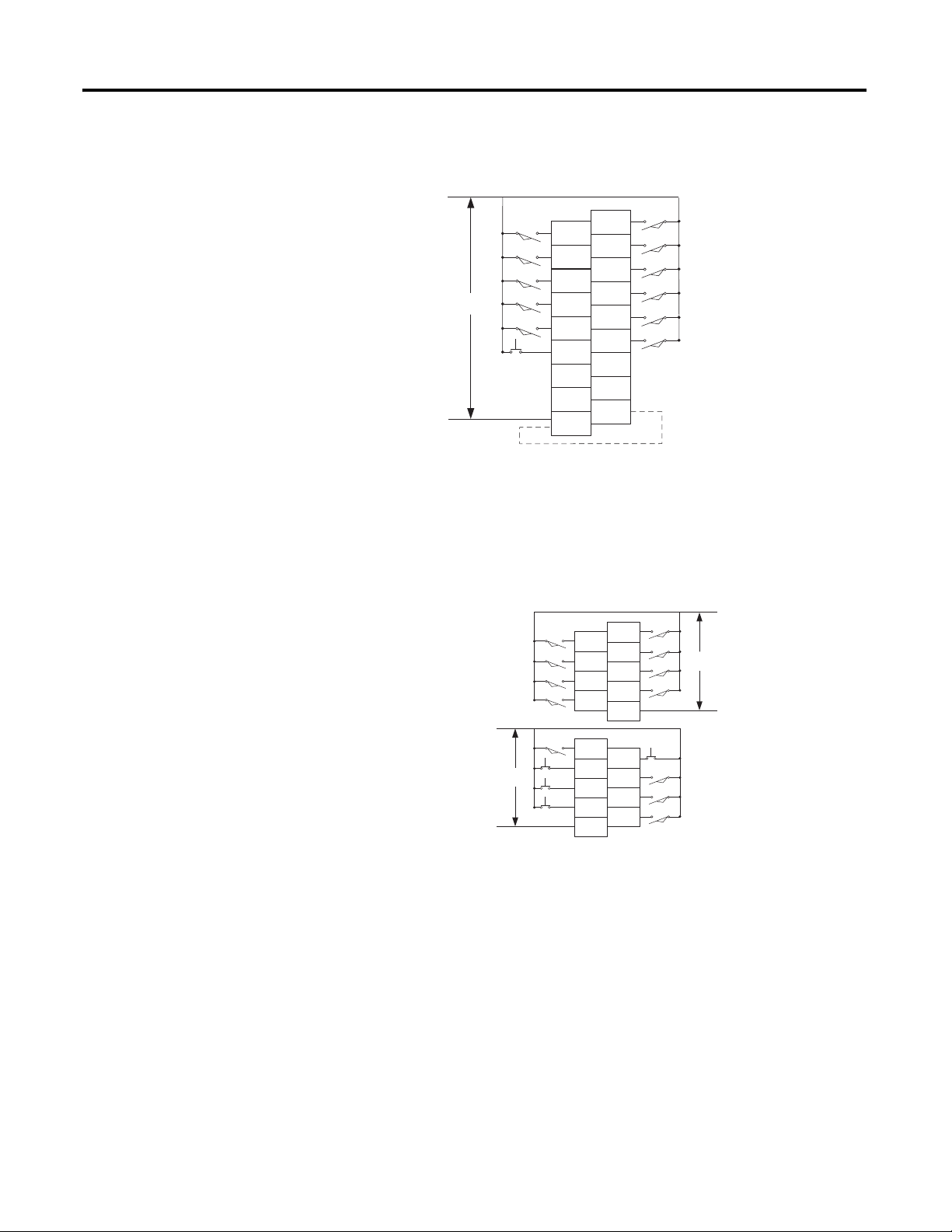
1769-IA8I
Chapter
2
1769-IA8I
Compact individually-isolated 120V AC input module
1769-IA16
Compact 120V AC input module
1769-IA16
L1
IN 0
IN 1
IN 2
IN 3
IN 4
IN 5
100/120V AC
L2
Rockwell Automation Publication 1769-IN088A-EN-P - February 2011 21
IN 7
IN 9
IN 11
IN 13
IN 15
AC
COM
IN 6
IN 8
IN 10
IN 12
IN 14
AC
COM
Commons are
connected internally.
Page 22
Chapter 2 Module Wiring
+
–
V in 0 +
V/I in 0 -
I in 0+
ANLG Com
V in 1 +
V/I in 1 -
I in 1+
ANLG Com
V in 2 +
V/I in 2 -
I in 2+
ANLG Com
V in 3 +
V/I in 3 -
I in 3+
ANLG Com
DC NEUT
+24V DC
+
-
1769-IF4 Differential Inputs
The external power supply must be rated Class 2, with a 24V DC
range of 20.4…26.4V DC and 60 mA minimum. Series B and
later modules support this option.
External 24V
DC Power
Supply
External 24V
DC Power
Supply
External 24V
DC Power
Supply
Analog Source
Belden 8761 Cable (or equivalent)
Earth ground the shield
locally at the module.
Sensor/
Transmitter
Supply
Current
Voltage
Voltage
Sensor/
Transmitter
Supply
Single-ended
Volt age
Differential
Voltage
Differential
Current
Tw o- wi re
Current
Signal
Signal
Ground
Signal
Ground
Signal
Signal
Signal
Signal
1769-IF4
22 Rockwell Automation Publication 1769-IN088A-EN-P - February 2011
Compact voltage/current analog input module
1769-IF4 Single-ended Sensor/Transmitter Inputs
+
-
+
+
–
–
–
+
1769-IF4 Mixed Transmitter Inputs
+
+
–
+
–
+
+
+
+
–
+
-
V in 0 +
V/I in 0 -
I in 0 +
ANLG Com
V in 1 +
V/I in 1 -
I in 1 +
ANLG Com
V in 2 +
V/I in 2 -
I in 2 +
ANLG Com
V in 3 +
V/I in 3 -
I in 3 +
ANLG Com
+24V DC
DC NEUT
V in 0 +
V/I in 0 -
I in 0 +
ANLG Com
V in 1 +
V/I in 1 -
I in 1 +
ANLG Com
V in 2 +
V/I in 2 -
I in 2 +
ANLG Com
V in 3 +
V/I in 3 -
I in 3 +
ANLG Com
+24V DC
DC NEUT
+
–
Page 23
Module Wiring Chapter 2
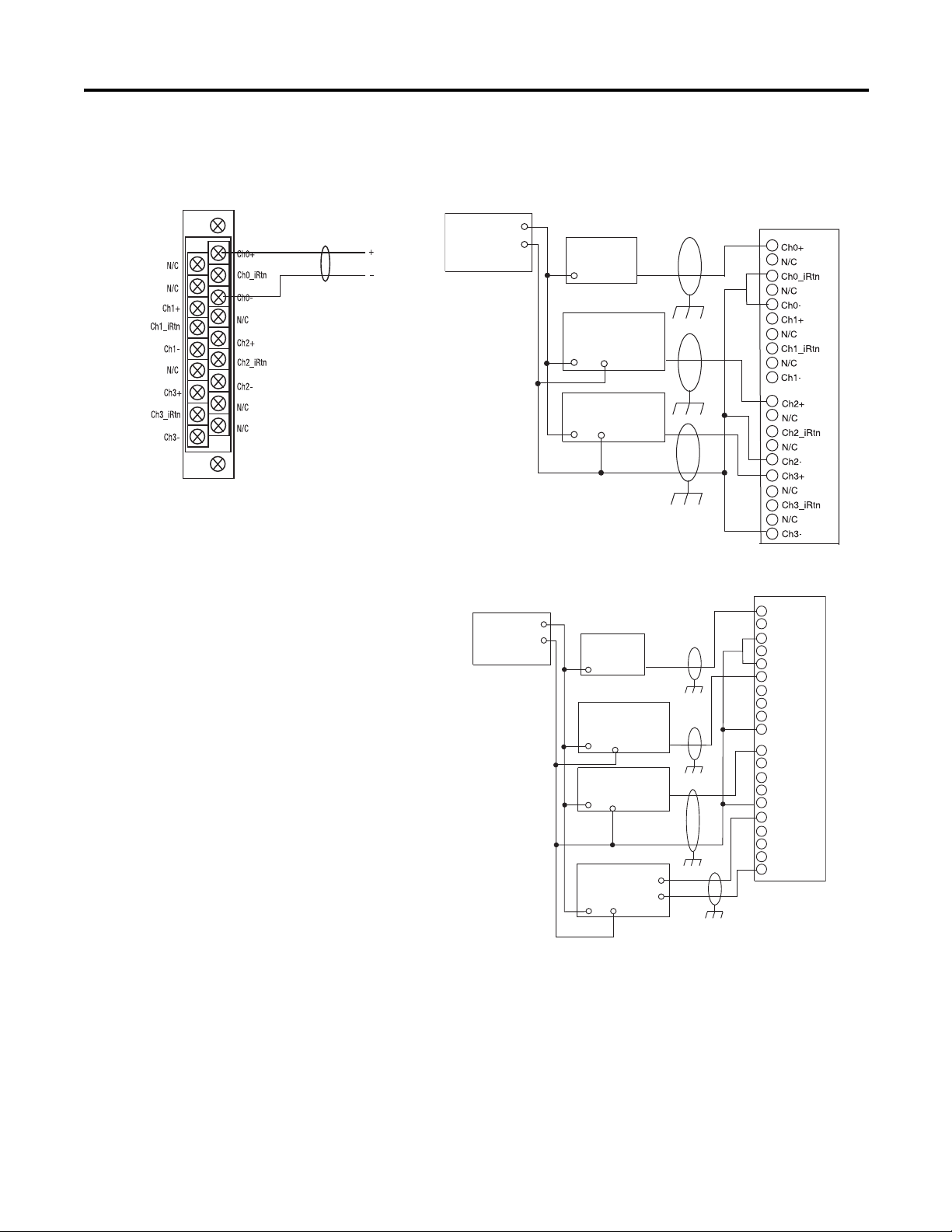
1769-IF4I Single-ended Sensor/Transmitter Inputs
+
+
+
+
-
Analog Source
Belden 8761 Cable (or equivalent)
Sensor/
Tr an sm it te r
Supply
Current
Voltage
Voltage
Sensor/
Transmitter
Supply
Differential
Voltage
Signal
Signal
Ground
Signal
Ground
Signal
Signal
Signal
Signal
Ground
Ground
Current
Voltage
Voltage
1769-IF4I
1769-IF4I Differential Inputs
Compact voltage/current analog, individually-isolated input module
1769-IF4I Mixed Transmitter Inputs
+
-
+
+
+
+
Ch0+
N/C
Ch0_iRtn
N/C
Ch0Ch1+
N/C
Ch1_iRtn
N/C
Ch1-
Ch2+
N/C
Ch2_iRtn
N/C
Ch2Ch3+
N/C
Ch3_iRtn
N/C
+
_
Ch3-
Rockwell Automation Publication 1769-IN088A-EN-P - February 2011 23
Page 24
Chapter 2 Module Wiring
1769-IF4XOF2 Differential Inputs
+
–
V in 1+
V in 3+
V in 0+
V/I in 0-
I in 1+
I in 3+
V/I in 1 -
I in 0+
I in 2+
V in 2 +
V/I in 3 -
V/I in 2-
ANLG Com
ANLG Com
V out 1+
I out 1+
V out 0+
I out 0+
1769-IF4XOF2 Outputs
V in 0+
V/I in 0 -
I in 0+
V in 1+
V/I in 1-
I in 1+
V in 2+
V/I in 2-
I in 2+
ANLG Com
ANLG Com
V in 3+
I out 0+
V out 0+
I out 1 +
V out 1+
V/I in 3-
I in 3+
Earth ground the shield
locally at the module.
Belden 8761 Cable (or equivalent)
Differential
Voltage
Tra ns mi tt er
Current
Voltage
Earth Ground
Earth Ground
1769-IF4XOF2 Single-ended Sensor/Tran smitter Inputs
+
V in 0+
V/I in 0 -
I in 0+
V in 1+
V/I in 1-
I in 1+
V in 2+
V/I in 2-
I in 2+
ANLG Com
ANLG Com
V in 3+
I out 0+
V out 0+
I out 1 +
V out 1+
V/I in 3-
I in 3+
+
+
-
1769-IF4XOF2 Mixed Transmitter Inputs
+
+
+
+
+
–
–
–
+
+–
–
–
V in 0+
V/I in 0 -
I in 0+
V in 1+
V/I in 1-
I in 1+
V in 2+
V/I in 2-
I in 2+
ANLG Com
ANLG Com
V in 3+
I out 0+
V out 0+
I out 1 +
V out 1+
V/I in 3-
I in 3+
Sensor/
Tra ns mi tt er
Supply
Sensor/
Transmitter
Supply
Current
Voltage
Signal
Signal
The sensor power supply must be rated Class 2.
Single-ended
Voltage
Differential
Voltage
Differential
Current
Tw o- wi re
Current
Signal
Signal
Signal
Signal
1769-IF4XOF2
Compact combination input/output analog module
24 Rockwell Automation Publication 1769-IN088A-EN-P - February 2011
Page 25
Module Wiring Chapter 2
Earth ground the shield
locally at the module.
Belden 8761 Cable (or equivalent)
Differential
Voltage
Transmitter
Differential
Current
Transmitter
Earth ground the shield
locally at the module.
The sensor power supply must be rated Class 2.
Simplified Input Circuit Diagram
Simplified Output Circuit Diagram
1769-IF4FXOF2F Single-ended Sensor/Tran smitter Inputs
+
V in 0+
V/I in 0 -
I in 0+
V in 1+
V/I in 1-
I in 1+
V in 2+
V/I in 2-
I in 2+
ANLG Com
ANLG Com
V in 3+
I out 0+
V out 0+
I out 1 +
V out 1+
V/I in 3-
I in 3+
+
+
-
Sensor/
Tra ns mi tt er
Supply
Sensor/
Transmitter
Supply
Current
Voltage
Signal
Signal
The sensor power supply must be rated Class 2.
Single-ended
Voltage
Differential
Voltage
Differential
Current
Tw o- wi re
Current
Signal
Signal
Signal
Signal
1769-IF4FXOF2F
Compact combination fast input/output analog module
1769-IF4FXOF2F Differential Inputs
V in 1+
V/I in 1 -
I in 1+
V in 3+
V/I in 3 -
I in 3+
ANLG Com
V out 1+
I out 1+
V in 0+
V/I in 0-
I in 0+
V in 2 +
V/I in 2-
I in 2+
ANLG Com
V out 0+
I out 0+
+
–
+
–
1769-IF4FXOF2F Mixed Transmitter Inputs
V in 0+
+
–
+
–
+–
+
–
–
+
Rockwell Automation Publication 1769-IN088A-EN-P - February 2011 25
+
+
–
I in 0+
V/I in 0 V in 1+
I in 1+
V/I in 1-
V in 2+
I in 2+
V/I in 2-
V in 3+
I in 3+
V/I in 3-
ANLG Com
ANLG Com
V out 0+
I out 0+
V out 1+
I out 1 +
Page 26
Chapter 2 Module Wiring
1769-IF4FXOF2F Outputs
V in 0+
V/I in 0 -
I in 0+
V in 1+
V/I in 1-
I in 1+
V in 2+
V/I in 2-
I in 2+
ANLG Com
ANLG Com
V in 3+
I out 0+
V out 0+
I out 1 +
V out 1+
V/I in 3-
I in 3+
Current
Voltage
Earth Ground
Earth Ground
26 Rockwell Automation Publication 1769-IN088A-EN-P - February 2011
Page 27
Module Wiring Chapter 2
+
–
–
The sensor power supply must be rated Class 2.
Analog SourceBelden 8761 Cable (or equivalent)
Earth ground the shield
locally at the module.
Sensor/
Transmitter
Supply
Current
Voltage
Voltage
Signal
Signal
Ground
Signal
Ground
Wiring for channels 4…7 are identical.
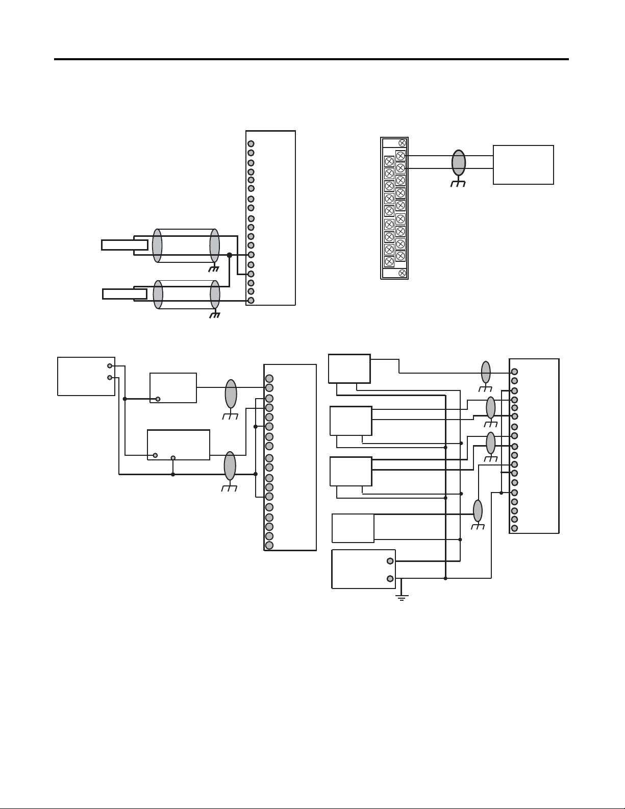
1769-IF8
V/I in 0-
ANLG Com
V/I in 1-
ANLG Com
V/I in 2-
ANLG Com
V/I in 3-
ANLG Com
1769-IF8 Differential Inputs
V in 0+
I in 0+
V in 1+
I in 1+
V in 2+
I in 2+
V in 3+
I in 3+
NC
NC
1769-IF8 Single-ended Sensor/Transmitter Inputs
+
-
+
+
+
Compact voltage/current analog input module
+
V/I in 4-
ANLG Com
V/I in 5-
ANLG Com
V/I in 6-
ANLG Com
V/I in 7-
ANLG Com
NC
V
V/I
I
ANLGC
V
V/I
I
ANLGC
V
V/I
I
ANLGC
V
V/I
I
ANLGC
NC
NC
V in 4+
I in 4+
V in 5+
I in 5+
V in 6+
I in 6+
V in 7+
I in 7+
NC
in
0
+
in
0
-
in
0
+
o
m
in
1
+
in
1
-
in
1
+
o
m
in
2
+
in
2
-
in
2
+
o
m
in
3
+
in
3
-
in
3
+
o
m
Rockwell Automation Publication 1769-IN088A-EN-P - February 2011 27
Page 28
Chapter 2 Module Wiring
1769-IF8 Mixed Transmitter Inputs
+
V in 0 +
V/I in 0 -
I in 0 +
ANLG Com
V in 1 +
V/I in 1 -
I in 1 +
ANLG Com
V in 2 +
V/I in 2 -
I in 2 +
ANLG Com
V in 3 +
V/I in 3 -
I in 3 +
ANLG Com
NC
NC
+
+
+
+
+
+
–
–
–
–
–
–
Sensor/
Transmitter
Supply
Single-ended
Voltag e
Differential
Voltage
Differential
Current
2-wire
Current
Signal
Signal
Signal
Signal
The sensor power supply must be rated Class 2.
Wiring for channels 4…7 are identical.
1769-IF16C Sensor/Transmittor Inputs
+
IN1+
IN0+
IN3+
IN2+
IN5+
IN4+
IN7+
IN8+
IN6+
IN9+
IN11+
IN10+
IN12+
IN13+
IN15+
IN14+
Com
Com
+
+
-
10 M
IN+
COM
0.1 μF
200
249
20 K
+
-
20 K
V
LOCALVLOCALVLOCAL
V
LOCAL
Gain A/D
M
u
l
t
i
p
l
e
x
e
r
The sensor power supply must be rated Class 2.
Sensor/
Transmitter
Supply
Current
Current
Signal
Signal
Ground
Simplified Input Circuit Diagram
1769-IF16C
28 Rockwell Automation Publication 1769-IN088A-EN-P - February 2011
Compact current analog input module
Page 29
Module Wiring Chapter 2
1769-IF16V Sensor/Transmittor Inputs
+
IN1+
IN0+
IN3+
IN2+
IN5+
IN4+
IN7+
IN8+
IN6+
IN9+
IN11+
IN10+
IN12+
IN13+
IN15+
IN14+
Com
Com
+
+
-
The sensor power supply must be rated Class 2.
Sensor/
Transmitter
Supply
Voltage
Voltage
Signal
Signal
Ground
Simplified Input Circuit Diagram
Simplified Input Circuit Diagram
· Use Belden 8761, or equivalent, shielded wire.
· Do not connect more than 2 wires to any single terminal.
· DC power cable and I/O cables should not exceed 10 m (30 ft).
· The capacitors shown above must be 0.01 µF and rated for 2000V min.
· User power supply must be rated Class 2 with a 5V DC range of
4.5…5.5V DC.
1769-IF16V
V
LOCAL
10 M
IN+
COM
200
20 K
0.1 μF
+
-
20 K
Compact voltage analog input module
V
LOCALVLOCALVLOCAL
M
u
Gain A/D
l
t
i
p
l
e
x
e
r
1769-IG16
Rockwell Automation Publication 1769-IN088A-EN-P - February 2011 29
Compact TTL input module
Page 30
Chapter 2 Module Wiring
IN 7
IN 5
IN 3
IN 1
AC
COM
IN 6
IN 4
IN 2
IN 0
L1
L2
200/240V AC
NC
NC
IN 10
IN 8
AC
COM
NC
NC
IN 11
IN 9
Commons are
connected internally.
1769-IM12
Do not use the NC terminals as a connection.
IN 7
IN 5
IN 3
DC
COM 1
IN 6
IN 4
+DC (sinking)
-DC (sourcing)
-DC (sinki ng)
+DC (sourcing)
+DC (si nki ng)
-DC (sourcing)
-DC (si nking)
+DC (so urci ng)
24V DC
IN 12
IN 14
IN 10
IN 8
IN 15
DC
COM 2
IN 13
IN 11
IN 9
24V DC
IN 1
IN 2
IN 0
1769-IQ16
1769-IM12
1769-IQ16
Compact 240V AC input module
Compact 24V DC sink/source input module
30 Rockwell Automation Publication 1769-IN088A-EN-P - February 2011
Page 31

Module Wiring Chapter 2
IN 7
IN 5
IN 3
DC
COM 1
IN 6
IN 4
+
DC (si nkin g)
-
DC (sourcing)
-
DC (si nkin g)
+
DC (sourcing)
+DC (sinking
)
-DC (sourcin
g)
-DC (si nking
)
+DC (sourcin
g)
24V DC
IN 12
IN 14
IN 10
IN 8
IN 15
DC
COM 2
IN 13
IN 11
IN 9
24V DC
IN 1
IN 2
IN 0
1769-IQ16F
1769-IQ16F
1769-IQ32
Compact 24V DC sink/source, high-speed input module
Compact 24V DC sink/source input module
1769-IQ32
+DC (Sinking)
– DC (Sourcing)
IN 0
IN 1
IN 2
IN 3
IN 4
IN 5
IN 6
IN 7
DC
COM 1
+ DC (Sinking)
– DC (Sourcing)
IN 9
24VDC
IN 11
IN 13
IN 15
DC
– DC (Sinking)
+ DC (Sourcing)
COM 2
– DC (Sinking)
+ DC (Sourcing)
IN 8
IN 10
IN 12
IN 14
24VDC
+ DC (Sinking)
– DC (Sourcing)
24VDC
– DC (Sinking)
+ DC (Sourcing)
IN 17
IN 19
IN 21
IN 23
IN 16
IN 18
IN 20
IN 22
DC
COM 3
IN 25
IN 27
IN 29
IN 31
DC
COM 4
+DC (Sinking)
– DC (Sourcing)
– DC (Sinking)
+ DC (Sourcing)
IN 24
IN 26
IN 28
IN 30
24VDC
Rockwell Automation Publication 1769-IN088A-EN-P - February 2011 31
Page 32

Chapter 2 Module Wiring
1769-IQ32T
1769-IQ32T
Compact 24V DC sink/source, terminated input module
32 Rockwell Automation Publication 1769-IN088A-EN-P - February 2011
Page 33

Module Wiring Chapter 2
3K
Vcc
IN
DC COM
536
0.1
μF
+24V
VAC-VDC
OUT
Simplified Input Circuit Diagram
Simplified Output Circuit Diagram
1769-IQ6XOW4
Compact combination 24V DC sink/source input and AC/DC relay output
module
1769-IQ6XOW4
+DC (sinking)
-DC (sourcing)
-DC (sinking)
+DC (sourcing)
24V DC
VAC
OUT 0
OUT 2
NC
NC
NC
IN 0
IN 2
IN 4
DC
COM
VDC
OUT 1
OUT 3
NC
NC
NC
IN 1
IN 3
IN 5
CR
CR
CR
CR
L1 or +DC
L2 or -DC
Rockwell Automation Publication 1769-IN088A-EN-P - February 2011 33
Page 34

Chapter 2 Module Wiring
EXC 3
SENSE 3
RTN 3
EXC 4
EXC 3
SENSE 3
RTN 3
EXC 4
EXC 3
SENSE 3
RTN 3
EXC 4
Two-wire RTD Configuration
Three-wire RTD Configuration
Add Jumper
Cable Shield (to Ground)
Return
RTD EXC
Return
RTD EXC
Belden 9501 Shielded Cable
Cable Shield (to Ground)
Sense
RTD EXC
Sense
RTD EXC
Belden 83503 or 9533 Shielded Cable
Return Return
Four-wire RTD Configuration
Cable Shield (to Ground)
Sense
RTD EXC
Sense
RTD EXC
Belden 83503 or 9533 Shielded Cable
Leave one sensor wire open.
Return Return
1769-IR6
Compact RTD/resistance input module
34 Rockwell Automation Publication 1769-IN088A-EN-P - February 2011
Page 35

EXC 3
EXC 3
SENSE 3
RTN 3
EXC 3
SENSE 3
RTN 3
Two-wire Potentiometer Configuration
Three-wire Potentiometer Configuration
Add Jumper
Cable Shield (to Ground)
Return
RTD EXC
Belden 9501 Shielded Cable
Run RTD EXC and sense wires from the module to
potentiometer terminal and tie terminal to one point.
Sense
RTD EXC
Belden 83503 or 9533 Shielded Cable
Return
Potentiometer
Potentiometer
Return
RTD EXC
Belden 9501 Shielded Cable
Cable Shield (to Ground)
Add Jumper
Potentiometer
Potentiometer
Belden 83503 or 9533 Shielded Cable
Sense
RTD EXC
Return
Cable Shield (to Ground)
Cable Shield (to Ground)
Run RTD EXC and sense wires from the module to
potentiometer terminal and tie terminal to one point.
SENSE 3
Module Wiring Chapter 2
RTN 3
EXC 3
SENSE 3
RTN 3
Rockwell Automation Publication 1769-IN088A-EN-P - February 2011 35
Page 36

Chapter 2 Module Wiring
NC
IN 0+
IN 0-
IN 3+
IN 1 +
IN 3-
IN 1-
IN 4+
IN 2+
IN 4-
IN 2-
IN 5+
IN 5-
NC
+
-
+
-
+
-
CJC 0+
CJC 0-
CJC 1-
CJC 1+
CJC Sensor
Ungrounded
Thermocouple
CJC Sensor
Grounded Thermocouple
Grounded Thermocouple
Within 10V DC
Z
OUT
VAC
470V
27
0.015μF
51
Vcc
150
Simplified Output Circuit Diagram
1769-IT6
1769-OA8
Compact Thermocouple/mV input module
Compact 100/240V AC solid state output module
1769-OA8
L1
100 to 240V AC
L2
36 Rockwell Automation Publication 1769-IN088A-EN-P - February 2011
CR
CR
CR
CR
OUT0
OUT2
VAC 2
OUT4
OUT6
VAC1
OUT1
OUT3
OUT5
OUT7
CR
CR
CR
CR
L1
100 to 240V AC
L2
Page 37

Module Wiring Chapter 2
100 to 240V AC
L2
L1
L2
L1
OUT10
OUT 8
VAC 2
OUT6
OUT4
OUT11
OUT 9
OUT 7
OUT 5
OUT 3
CR
CR
CR
CR
CR
CR
CRCRCR
CR
CR
CR
CR
CR
100 to 240V
AC
VAC 1
OUT 1
OUT 0
OUT 2
CR
CR
CRCRCR
CRCRCR
OUT 12
OUT 14
OUT 13
OUT 15
1769-OA16
Simplified Output Circuit Diagram
DC+
DC-
OUT 6
OUT 4
NC
NC
NC
OUT 2
OUT 0
OUT 7
OUT 5
+VDC 2
NC
NC
NC
OUT 3
OUT 1
+VDC 1
CR
CR
CR
CR
DC COM
2
DC COM
1
CR
CR
DC -
DC+
1769-OB8
VCC
ASIC
VDC
OUT
COM
Simplified Output Circuit Diagram
Logic Side User Side
1769-OA16
1769-OB8
Vcc
Compact 120/240V AC solid state output module
51
VAC
Z
150
27
0.015 μF
470V
OUT
Compact solid state 24V DC source, high-current output module
Rockwell Automation Publication 1769-IN088A-EN-P - February 2011 37
Page 38

Chapter 2 Module Wiring
+DC
24V D C(source)
-DC
DC COM
OUT 14
OUT 12
OUT 10
OUT 8
OUT 6
OUT 4
OUT 2
OUT 0
OUT 15
OUT 13
OUT 11
OUT 9
OUT 7
OUT 5
OUT 3
OUT 1
+VDC
CR
CR
CR
CR
CR
CR
CR
CR
CR
CR
1769-OB16
Vcc
+VDC
OUT
DC COM
0.1μF
100pF
20K
15K
10K
G
S
D
Simplified Output Circuit Diagram
+VDC
OUT
DC COM
39V
39V
Vcc
47K
100pF
6V
Voltage
Regulator
Simplified Output Circuit Diagram
Protection circuit is not shown.
1769-OB16
1769-OB16P
Compact solid state 24V DC source output module
Compact solid state 24V DC source, protected output module
1769-OB16P
38 Rockwell Automation Publication 1769-IN088A-EN-P - February 2011
CR
CR
CR
CR
OUT 2
OUT 4
OUT 6
OUT 8
OUT 10
OUT 12
OUT 14
DC COM
OUT 1
OUT 3
OUT 5
OUT 7
OUT 9
OUT 11
OUT 13
OUT 15
CR
CR
CR
CR
CR
CR
+VDC
OUT 0
+DC
24V DC
-DC
Page 39

Module Wiring Chapter 2
VCC
ASIC
VDC
OUT
COM
TR1
G
S
D
Simplified Output Circuit Diagram
Logic Side User Side
Simplified Output Circuit Diagram
Logic Side User Side
1769-OB32
Compact solid state 24V DC source output module
1769-OB32
24V DC
+DC
-DC
CR
CR
CR
CR
OUT 18
OUT 20
OUT 22
OUT 24
OUT 26
OUT 28
OUT 30
DC
COM 2
OUT 17
OUT 19
OUT 21
OUT 23
OUT 25
OUT 27
OUT 29
OUT 31
+VDC 2
OUT 16
CR
CR
CR
CR
OUT 2
OUT 4
OUT 6
OUT 8
OUT 10
OUT 12
OUT 14
DC
COM 1
OUT 1
OUT 3
OUT 5
OUT 7
OUT 9
OUT 11
OUT 13
OUT 15
CR
CR
CR
CR
CR
CR
+VDC 1
OUT 0
+DC
CR
CR
CR
24V DC
CR
CR
CR
-DC
1769-OB32T
VCC
ASIC
Compact solid state 24V DC source, terminated output module
S
G
D
Rockwell Automation Publication 1769-IN088A-EN-P - February 2011 39
TR1
VDC
OUT
COM
+VDC 1
+VDC 1
1769-OB32T
+VDC 2
+VDC 2
V DC42 V DC42
Page 40

Chapter 2 Module Wiring
The external power supply must be rated Class 2, with a 24V DC
range of 20.4…26.4V DC and 60 mA minimum. Series B and
later modules support this option.
Earth Ground
External 24V DC
Power Supply
Current
Earth Ground
Voltage
V out 3+
ANLG Com
ANLG Com
I out 3+
I out 0+
V out 0+
I out 1 +
V out 1+
I out 2+
V out 2+
16-pin Backplane Connector
ASIC
Indicator
Isolated
DC to DC
Converter
Optocouplers
CPU
D to A
Converter
Voltage
Output
Current
Output
18-pin Terminal Block
+15V
+5V
-15V
GND
Isolation
Voltage Load
Current Load
Earth Ground
Earth Ground
Simplified Schematic
1769-OF2
1769-OF4
Compact voltage/current output analog module
1769-OF2
V out 0 +
I out 0 +
ANLG Com
NC
V out 1 +
I out 1 +
ANLG Com
NC
+
-
+24V DC
DC NEUT
Compact voltage/current output analog module
40 Rockwell Automation Publication 1769-IN088A-EN-P - February 2011
Page 41

Module Wiring Chapter 2
1769-OF4CI
Current
Earth Ground
1769-OF4VI
Earth Ground
Voltage
1769-OF4CI
Compact current output, individually isolated analog module
1769-OF4VI
Compact voltage output, individually isolated analog module
Rockwell Automation Publication 1769-IN088A-EN-P - February 2011 41
Page 42

Chapter 2 Module Wiring
Current
Earth Ground
The external power supply must be rated Class 2, with a 24V DC range of 20.4…6.4V DC
and 60 mA minimum. Series B and later modules support this option.
External 24V DC Power
Supply (optional)
1769-OF8C
Compact current output analog module
I out 0+
I out 1+
I out 2+
I out 3+
I out 4+
+
-
I out 5+
I out 6+
I out 7+
+24V DC
1769-OF8C
ANLG Com
ANLG Com
ANLG Com
ANLG Com
ANLG Com
ANLG Com
ANLG Com
ANLG Com
DC NEUT
42 Rockwell Automation Publication 1769-IN088A-EN-P - February 2011
Page 43

Module Wiring Chapter 2
Voltage
Earth Ground
The external power supply must be rated Class 2, with a 24V DC range of 20.4…6.4V DC
and 60 mA minimum. Series B and later modules support this option.
External 24V DC Power
Supply (optional)
1769-OF8V
Compact voltage output analog module
V out 0+
V out 1+
V out 2+
V out 3+
V out 4+
+
-
V out 5+
V out 6+
V out 7+
+24V DC
1769-OF8V
ANLG Com
ANLG Com
ANLG Com
ANLG Com
ANLG Com
ANLG Com
ANLG Com
ANLG Com
DC NEUT
Rockwell Automation Publication 1769-IN088A-EN-P - February 2011 43
Page 44

Chapter 2 Module Wiring
Simplified Output Circuit Diagram
· Use Belden 8761, or equivalent, shielded wire.
· Do not connect more than two wires to any single terminal.
· DC power cable and I/O cables should not exceed 10 m (30 ft).
· The capacitors shown above must be 0.01 µF and rated for 2000V min.
· User power supply must be rated Class 2 with a 5V DC range of
4.5…5.5V DC.
Vcc
+VDC
OUT
DC COM
0.1μF
100pF
10K
6.8 K
4.7 K
G
S
D
Simplified Output Circuit Diagram
1769-OG16
Compact TTL output module
1769-OV16
44 Rockwell Automation Publication 1769-IN088A-EN-P - February 2011
Compact solid state 24V DC sink output module
1769-OV16
OUT 0
CR
OUT 2
CR
OUT 4
CR
OUT 6
OUT 8
CR
OUT 10
OUT 12
OUT 14
DC COM
+VDC
OUT 1
OUT 3
OUT 5
OUT 7
OUT 9
OUT 11
OUT 13
OUT 15
CR
CR
CR
CR
CR
CR
+DC
24V DC (sink)
-DC
Page 45

Module Wiring Chapter 2
~
+VDC
OUT
DC COM
Simplified Output Circuit Diagram
L2 or -DC
L1 or +DC
L2 or -DC
L1 or +DC
OUT 6
OUT 4
VAC-VDC
2
OUT 2
OUT 0
OUT 7
OUT 5
OUT 3
OUT 1
VAC-VDC
1
CR
CR
CR
CR
CR
CR
1769-OW8
Simplified Output Circuit Diagram
1769-OV32T
1769-OW8
Compact solid state 24V DC sink, terminated output module
1769-OV32T
+VDC 1
+VDC 1
Compact AC/DC relay contact module
+VDC 2
+VDC 2
+24V
VAC -VDC
OUT
Rockwell Automation Publication 1769-IN088A-EN-P - February 2011 45
Page 46

Chapter 2 Module Wiring
L1a or +DCa
L2a or -DCa
OUT 0
OUT 6
OUT 5
OUT 4
OUT 3
OUT 7
VAC-VDC
5
VAC-VDC
4
VAC-VDC
3
VAC-VDC
6
NC
VAC-VDC
7
NC
VAC-VDC
0
CR
L1b or +DCb
L2b or -DCb
OUT 1
VAC-VDC
1
L1c or +DCc
L2c or -DCc
OUT 2
VAC-VDC
2
1769-OW8I
Simplified Output Circuit Diagram
L1 or +DC
OUT 10
OUT 8
VAC-VDC
2
OUT 6
OUT 4
OUT 11
OUT 9
OUT 3
OUT 1
VAC-VDC
1
L1 or +DC
CR
CR
CR
CR
CR
CR
CR
CR
CR
CR
L2 or -DC
L2 or -DC
OUT 0
OUT 2
OUT 5
OUT 7
OUT 12
OUT 14
OUT 13
OUT 15
1769-OW16
+24V
VAC -VDC
OUT
Simplified Output Circuit Diagram
1769-OW8I
1769-OW16
Compact AC/DC individually isolated, relay contact module
+24V
VAC-VDC
OUT
Compact AC/DC relay contact module
1769-ARM
46 Rockwell Automation Publication 1769-IN088A-EN-P - February 2011
The 1769-ARM module is an address reserve module for reserving I/O module
slots. As a result, no wiring is required.
Page 47

Module Wiring Chapter 2
NC1
RXD2
TXD3
NC4
COM5
NC6
RTS7
CTS8
NC9
DCD
TXD
RSD
DSR
COM
DTR
CTS
RTS
GND
8
2
3
6
7
20
5
4
1
1
3
2
6
5
4
8
7
ASCII DTE DTE 9-pin 25-pin
TXD-
NC
NC
1
2
3
4
COM5
RXD+
RTS
CTS
6
7
8
TXD+9
RXD-
TXDCOM
TXD+
RXD+
RXD-
ASCII
NC
NC
NC
1
RXD2
TXD3
4
COM5
6
RTS7
CTS8
N.C.9
CD
TXD
RXD
DSR
COM
DTR
CTS
RTS
RI
8
2
3
6
7
20
5
4
22
1
3
2
6
5
4
8
7
9
GND 1
ASCII DTE DTE 9-pin 25-pin
TRXD-
NC
NC
NC
NC
1
2
3
4
COM
RTS
CTS
5
6
7
8
TRXD+9
TRXD-
COM
TRXD+
ASCII
RS-232 Wiring Module to DTE Device (hardware handshaking disabled)
RS-232 Wiring Module to Printer (hardware handshaking enabled, standard
printer adapter cable)
RS-422 Wiring
RS-485 Wiring
1769-ASCII
Compact ASCII module
Rockwell Automation Publication 1769-IN088A-EN-P - February 2011 47
Page 48

Chapter 2 Module Wiring
+VDC
OUT DC COM
OUT x
Simplified Input Schematic
Simplified Output Schematic
Do not use the NC terminals
as connection points.
A
A
B
B
Z
Z
A1(+)
A1(–)
B1(+)
B1(–)
Z1(+)
Z1(–)
GND
VS
+VDC
COM
Cable
Power
Supply
Allen-Bradley
845H Series
differential
encoder.
Shield/Housing
Connect only if housing is electronically
isolated from the motor and ground.
Shield
Module Inputs
Earth
Differential Encoder Wiring
Use twisted-pair, individually-shielded cable with
a maximum length of 300 m (1000 ft).
1769-BOOLEAN
Compact combination 24V DC sink input/source output BOOLEAN control
module
1769-HSC
48 Rockwell Automation Publication 1769-IN088A-EN-P - February 2011
Compact high-speed counter module
Page 49

Module Wiring Chapter 2
Single-ended Encoder Wiring
A
B
Z
A1(+)
A1(–)
B1(+)
B1(–)
Z1(+)
Z1(–)
GND
VS
+VDC
COM
R
(2)
Cable
Power
Supply
Allen-Bradley
845H Series
single-ended
encoder.
Shield/Housing
Connect only if housing is electronically
isolated from the motor and ground.
Shield
Module Inputs
Earth
Use twisted-pair, individually-shielded cable with
a maximum length of 300 m (1000 ft).
R
V
dcVmin–()
Imin
--------------------------------------=
External resistors are required if they are not internal to the encoder. The pull-up resistor (R) value
depends on the power supply value. To calculate the maximum resistor value, use this formula:
where:
· R = maximum pull-up resistor value
· Vdc = power supply voltage
· Vmin = 2.6V DC
· min = 6.8 mA
Power Supply Voltage
Pull-up Resistor Value Max (R)
5V DC 352 Ω
12V DC 1382 Ω
24V DC 3147 Ω
(1) Resistance values may change, depending upon your application.
Rockwell Automation Publication 1769-IN088A-EN-P - February 2011 49
(1)
Page 50

Chapter 2 Module Wiring
VS
A1(+)
A1(–)
B1(+)
B1(–)
Z1(+)
Z1(–)
+VDC
COM
VS
OUT
COM
OUT
COM
VS
OUT
COM
R
(1)
Discrete Device Wiring
Power
Supply
Module Inputs
Solid-State
Switch
Proximity Sensor
Photoelectric Sensor
with Open Collector
Sinking Output
R
V
dcVmin–()
Imin
--------------------------------------=
The minimum resistor (R) value depends on the current sinking capability of the encoder.
External resistors are required if they are not internal to the encoder. The pull-up resistor (R) value
depends on the power supply value. To calculate the maximum resistor value, use this formula:
50 Rockwell Automation Publication 1769-IN088A-EN-P - February 2011
where:
· R = maximum pull-up resistor value
· Vdc = power supply voltage
· Vmin = 2.6V DC
· min = 6.8 mA
Power Supply Voltage
Pull-up Resistor Value Max (R)
5V DC 352 Ω
12V DC 1382 Ω
24V DC 3147 Ω
(1) Resistance values may change, depending upon your application.
The minimum resistor (R) value depends on the current sinking capability of the encoder.
(1)
Page 51

CR
Output Wiring
OUT 0
OUT 2
OUT
DC COM
A0-
B0-
Z0-
A1-
B1-
Z1-
OUT DC
+5/24V DC
OUT 1
OUT 3
A0+
B0+
Z0+
A1+
B1+
Z1+
Module Wiring Chapter 2
+DC
CR
CR
+5/24V DC
-DC
Rockwell Automation Publication 1769-IN088A-EN-P - February 2011 51
Page 52

Chapter 2 Module Wiring
Notes:
52 Rockwell Automation Publication 1769-IN088A-EN-P - February 2011
Page 53

I/O Memory Mapping
I/O Type Cat. No. Page
AC digital 1769-IA8I
1769-IA16
1769-IM12
1769-OA8
1769-OA16
DC digital 1769-IG16
1769-IQ16
1769-IQ16F
1769-IQ32
1769-IQ32T
1769-IQ6XOW4
1769-OB8, Series A
1769-OB16, Series B
1769-OB16P
1769-OB32
1769-OB32T
1769-OG16
1769-OV16
1769-OV32T
Contact 1769-OW8
1769-OW8I
1769-OW16
Analog 1769-IF4
1769-IF4I
1769-IF4XOF2
1769-IF4FXOF2F
1769-IF8
1769-IF16C
1769-IF16V
1769-IR6
1769-IT6
1769-OF2
1769-OF4
1769-OF4CI
1769-OF4VI
1769-OF8C
1769-OF8V
Specialty 1769-ARM
1769-ASCII
1769-BOOLEAN
1769-HSC
54
54
94
107
110
92
94
95
96
96
97
113
116
119
122
125
162
165
167
170
173
176
55
57
61
65
70
80
86
100
104
128
132
135
139
142
152
179
180
187
195
Chapter
3
Rockwell Automation Publication 1769-IN088A-EN-P - February 2011 53
Page 54

Chapter 3 I/O Memory Mapping
1769-IA8I
1769-IA16
The following I/O memory mapping lets you configure the 1769-IA8I module.
Input Data File
For each input module, slot x, word 0 in the input data file contains the current
state of the field input points. For the 1769-IA8I, bits 8 to 15 are not used.
Bit Position
1514131211109876543210
Word
0
0 0 0 0 0 0 0 0r
(1) r = read.
(1)
rrrrrrr
The following I/O memory mapping lets you configure the 1769-IA16 module.
Input Data File
For each input module, slot x, word 0 in the input data file contains the current
state of the field input points.
Bit Position
1514131211109876543210
Word
(1)
0r
(1) r = read.
rrrrrrrrrrrrrrr
54 Rockwell Automation Publication 1769-IN088A-EN-P - February 2011
Page 55

I/O Memory Mapping Chapter 3
1769-IF4
The following I/O memory mapping lets you configure the 1769-IF4 module.
Input Data File
For each input module, slot x, words 0…3 in the input data file contain the analog
values of the inputs.
Bit Position
15 14131211109876543210
Word
0 SGN Analog Input Data Channel 0
1 SGN Analog Input Data Channel 1
2 SGN Analog Input Data Channel 2
3 SGN Analog Input Data Channel 3
4 Not Used S3 S2 S1 S0
5 U0 O0U101U2O2U3O3Set to 0
The bits are defined as follows:
• SGN = Sign bit in two’s complement format.
• Sx = General status bit for channels 0 through 3. This bit is set (1) when an
error (over- or under-range) exists for that channel.
• Ux = Under-range flag bits for channels 0 through 3. These bits can be
used in the control program for error detection.
• Ox = Over-range flag bits for channels 0 through 3. These bits can be used
in the control program for error detection.
Configuration Data File
The manipulation of the bits from this file is normally done with programming
software, such as RSLogix 500, RSLogix 5000, or RSNetWorx for DeviceNet,
during initial configuration of the system. In that case, graphical screens are
provided by the programmer to simplify configuration. However, some systems,
like the 1769-ADN DeviceNet adapter, also allow the bits to be altered as part of
the control program using communication rungs. In that case, it is necessary to
understand the bit arrangement. Refer to the Compact I/O Analog Modules
User Manual, publication number 1769-UM002
Rockwell Automation Publication 1769-IN088A-EN-P - February 2011 55
for additional details.
Page 56

Chapter 3 I/O Memory Mapping
Words 0……3 of the configuration file allow you to change the parameters of each
channel independently. For example, word 0 corresponds to channel 0.
Define To Select Make these bit settings
15 14 13 12 11 10 9 8 4…73210
Input Filter
Selection/-3 dB
Frequency
60 Hz/15.7 Hz
50 Hz/13.1 Hz
Not Used 0010
250 Hz/65.5 Hz 0011
500 Hz/131Hz
(1)
Spare
Input Type/
Range
-10 to +10V dc 0000
0 to 5V dc 0001
0 to 10V dc 0010
4 to 20 mA 0011
1 to 5V dc 0100
0 to 20 mA 0101
(1)
Spare
Input Data
Format
Raw/Proportional
Data
Engineering
Units
Scaled-for-PID 010
Percent Range 011
(1)
Spare
Enable Channel Enabled 1
Disabled 0
0000
0001
0100
Not Used
000
001
(1) An attempt to write any nonvalid (spare) bit configuration into any selection field results in a module
configuration error.
56 Rockwell Automation Publication 1769-IN088A-EN-P - February 2011
Page 57

I/O Memory Mapping Chapter 3
1769-IF4I
The following I/O memory mapping lets you configure the 1769-IF4I module.
Input Data File
For each input module, slot x, words 0…3 in the input data file contain the analog
values of the inputs.
Bit Position
15 14131211109876543210
Word
0 SGN Analog Input Data Channel 0
1 SGN Analog Input Data Channel 1
2 SGN Analog Input Data Channel 2
3 SGN Analog Input Data Channel 3
4 Nu Time Stamp Value
5 Nu NuNuNuNuNuNuNuNuNuNuNuS3S2 S1S0
6 L3 H3U3O3L2 H2U2O2L1 H1U1O1L0 H0U0O0
The bits are defined as follows:
• SGN = Sign bit in two’s complement format.
• Nu = Not used. Bit set to 0.
• Sx = General status bit for input channels 0…3.
• Lx = Low alarm flag bits for input channels 0…3.
• Hx = High alarm flag bits for input channels 0…3.
• Ux = Under-range flag bits for channels 0…3. When set, the input signal is
under normal range or an open circuit condition exists, in the case of the 420 mA range.
• Ox = Over-range flag bits for channels 0…3. When set, the input signal is
over normal range or an open circuit condition exists. Open circuit
detection applies to voltage input ranges only.
Rockwell Automation Publication 1769-IN088A-EN-P - February 2011 57
Page 58

Chapter 3 I/O Memory Mapping
Output Data File
For each input module, slot x, word 0 in the output data file contains the analog
values of the outputs.
Bit Position
1514131211109876543210
Word
0 Nu Nu Nu Nu Nu Nu Nu Nu UL3 UH3 UL2 UH2 UL1 UH1 UL0 UH0
The bits are defined as follows:
• Nu = Not used. Bit set to 0.
• UHx = Cancel High Process Alarm Latch x. Allows each high process
alarm latch to be individually cancelled. Cancel = 1.
• ULx = Cancel Low Process Alarm Latch x. Allows each low process alarm
latch to be individually cancelled. Cancel = 1.
Configuration Data File
The manipulation of the bits from this file is normally done with programming
software, such as RSLogix 500, RSLogix 5000, or RSNetWorx for DeviceNet,
during initial configuration of the system. In that case, graphical screens are
provided by the programmer to simplify configuration. However, some systems,
like the 1769-ADN DeviceNet adapter, also allow the bits to be altered as part of
the control program, using communication rungs. In that case, it is necessary to
understand the bit arrangement.
Bit Position
1514131211109 876543210
Word
0 Real Time Sample Value
1 ETS Reserved
2 EC Reserved EA AL EI Reserved Input Filter Sel Chl0
3 Reserved Inpt Dta Fm
Chl0
4 S Process Alarm High Data Value Channel 0
5 S Process Alarm Low Data Value Channel 0
6 S Alarm Dead Band Value Channel 0
7 Reserved
8 EC Reserved EA AL EI Reserved Inpt Filter Sel Chl1
9 Reserved Inpt Dta Fm
Chl1
10 S Process Alarm High Data Value Channel 1
11 S Process Alarm Low Data Value Channel 1
12 S Alarm Dead Band Value Channel 1
Reserved Inpt Tp/RngeSel
Chl0
Reserved Inpt Tp/RngeSel
Chl1
58 Rockwell Automation Publication 1769-IN088A-EN-P - February 2011
Page 59

I/O Memory Mapping Chapter 3
Bit Position
15141312111098 76543210
Word
13 Reserved
14 EC Reserved EA AL EI Reserved Input Filter Sel Chl2
15 Reserved Inpt Dta Fm
Chl2
16 S Process Alarm High Data Value Channel 2
17 S Process Alarm Low Data Value Channel 2
18 S Alarm Dead Band Value Channel 2
19 Reserved
20 EC Reserved EA AL EI Reserved Input Filter Sel Chl3
21 Reserved Inpt Dta Fm
Chl3
22 S Process Alarm High Data Value Channel 3
23 S Process Alarm Low Data Value Channel 3
24 S Alarm Dead Band Value Channel 3
25 Reserved
Reserved Inpt Tp/RngeSel
Chl2
Reserved Inpt Tp/RngeSel
Chl3
The bits are defined as follows:
• EC = Enable Channel.
• Inpt Dta Fm Chlx = Input Data Format Select.
• EA = Enable Alarm.
• AL = Alarm Latch.
• EI = Enable Interrupt.
(1)
• Inpt Tp/Rnge Sel Chlx = Input Type/Range Select.
• Inpt Filter Sel Chlx = Input Filter Select.
• Reserved = Allows for future expansion.
• ETS = Enable Time Stamp.
(1) MicroLogix 1500 and CompactLogix L3x controllers do not support interrupts.
Rockwell Automation Publication 1769-IN088A-EN-P - February 2011 59
Page 60

Chapter 3 I/O Memory Mapping
Define To Select Make these bit settings
15 14…11 10 9 8 7…4 3 2 1 0
Input Filter Selection 60 Hz
50 Hz 0001
28.5 Hz 0010
300 Hz
360 Hz 0100
Enable Interrupt Enable 1
Disable 0
Enable Process
Alarm Latch
Enable Process Alarms Enable 1
Enable Channel Enable 1
Enable 1
Disable 0
Disable 0
Disable 0
0000
0011
Define Indicate this These bit settings
15…11 10 9 8 7…4 3 2 1 0
Input Range Select -10…+10V dc
0…5V dc 0001
0…10V dc
4…20 mA 0011
1…5V dc 0100
0…20 mA
Input Data Select Raw/Proportional
Counts
Engineering Units 0 0 1
Scaled for PID 0 1 0
Percent Range 0 1 1
000
0000
0010
0101
60 Rockwell Automation Publication 1769-IN088A-EN-P - February 2011
Page 61

I/O Memory Mapping Chapter 3
IMPORTANT
1769-IF4XOF2
The following I/O memory mapping lets you configure the 1769-IF4XOF2
module.
Input Data File
The input data file provides access to input data for use in the control program,
over-range indication for the input and output channels, and output data
feedback as described below.
Bit Position
15 14 13 12 11 10 9 8 7 6 5 4 3 2 1 0
Word
0 SGN Analog Input Data Channel 0 0 0 0 0 0 0 0
1 SGN Analog Input Data Channel 1 0 0 0 0 0 0 0
2 SGN Analog Input Data Channel 2 0 0 0 0 0 0 0
3 SGN Analog Input Data Channel 3 0 0 0 0 0 0 0
4 Not Used
5Not
Used
6 SGN Output Data Echo/Loopback for Output Channel 0 0 0 0 0 0 0 0
7 SGN Output Data Echo/Loopback for Output Channel 1 0 0 0 0 0 0 0
(1)
H0 Not
Used
H1 Not Used
I3 I2 I1 I0
()
E1 E0 O1 O0
(1) All unused bits are set to 0 by the module.
Input words 6 and 7 contain the output data echo/loopback information
for output channels 0 and 1 respectively. Bits 0 through 6 and Bit 15 of
words 6 and 7 should always be set to zero in your control program. If
they are not set to 0, the invalid data flag (Ex) will be set for that channel
by the module. However, the channel will continue to operate with the
previously converted value.
The bits are defined as follows:
• SGN = Sign bit in two’s complement format. Always positive (equal to
zero) for the 1769-IF4XOF2 module.
• Ix = Over-range flag bits for input channels 0 through 3. These bits can be
used in the control program for error detection. When set to 1, the bits
signal that the input signal is outside the normal operating range. However,
the module continues to convert analog data to the maximum full-range
value. When the over-range condition is cleared, the bits automatically
reset (0).
Rockwell Automation Publication 1769-IN088A-EN-P - February 2011 61
Page 62

Chapter 3 I/O Memory Mapping
TIP
IMPORTANT
IMPORTANT
• Ox = Word 5, bits 0 and 1 provide over-range indication for output
channels 0 and 1. These bits can be used in the control program for error
detection. When set to 1, the bits signal that the output signal is outside
the normal operating range. However, the module continues to convert
analog data to the maximum full-range value. When the over-range
condition is cleared, the bits automatically reset (0).
Under-range indication is not provided because zero is a valid
number.
• Ex = When set (1), this bit indicates that invalid data has been set in the
output data bits 0 through 6 or the sign bit (15). For example, the value
sent by the controller is outside the standard output range or increment,
such as 128, 256.
• Hx = Hold Last State bits. When set (1), these bits indicate that the
channel is in a Hold Last State condition.
• Words 6 and 7 = These words reflect the analog output data echo of the
analog value being converted by the digital/analog converter, not
necessarily the electrical state of the output terminals. They do not reflect
shorted or open outputs.
It is only important to use the loopback function of input words 6
and 7 if the controller supports the Program mode or Fault mode
functions, and if it is configured to use them.
Output Data File
The output data file applies only to output data from the module as shown in the
table below.
Bit Position
15 14131211109876543210
Word
0SGN Analog Output Data Channel 0 0000000
1SGN Analog Output Data Channel 1 0000000
Bits 0 through 6 and Bit 15 of output data words 0 and 1 should always
be set to zero in your control program. If they are not set to 0, the invalid
data flag (Ex) will be set for that channel. However, the channel will
continue to operate with the previously converted value. If a MVM (Move
with Mask) instruction is used with a mask of 7F80 (hexidecimal) to move
data to the output words, writing to bits 0 through 6 and bit 15 can be
avoided.
62 Rockwell Automation Publication 1769-IN088A-EN-P - February 2011
Page 63

I/O Memory Mapping Chapter 3
TIP
Configuration Data File
The manipulation of the bits from this file is normally done with programming
software, such as RSLogix 500, RSLogix 5000, or RSNetWorx for DeviceNet,
during initial configuration of the system. In that case, graphical screens are
typically provided by the programmer to simplify configuration. However, some
systems, like the 1769-ADN DeviceNet adapter, also allow the bits to be altered
as part of the control program, using communication rungs. In that case, it is
necessary to understand the bit arrangement. Refer to the Compact Analog I/O
Combination Module User Manual, publication number
1769-UM008
Bit Position
15 14 13 12 11 10 9 8 7 6 5 4 3 2 1 0
Word
0Not
Used
1Not
Used
2 SGN Channel 0 Fault Value
3 SGN Channel 0 Program (Idle) Value
4 SGN Channel 1 Fault Value
5 SGN Channel 1 Program (Idle) Value
for additional details.
Not
(1)
Used
Not
(1)
Used
(1)
(1)
Not Used
Not Used
(1)
EI3 EI2 EI1 EI0 FM0
(1)
Not
Not
(1)
Used
(2)
(2)
(2)
(2)
EO1 EO0 FM1
(1)
Used
0000000
0000000
0000000
0000000
(2)
(2)
PM0
Not
PFE0
(1)
Used
(2)
(2)
PM1
Not
PFE1
(1)
Used
(2)
(2)
(1) Any attempt to write a nonvalid (1s) bit configurations into any not used selection field results in a module
configuration error.
(2) Not all controllers support these functions. Refer to your controller’s user manual for details.
The bits are defined as follows:
• SGN = Sign bit in two’s complement format. The sign of the data for the
1769-IF4XOF2 must be positive (Bit 15 = 0) or a configuration error
occurs.
• EIx = Individually enable or disable input channels 0 through 3 using these
bits. When a channel is not enabled, the module provides no current or
voltage input to the host controller.
• EOx = Individually enable or disable output channels 0 and 1 using these
bits. When a channel is not enabled, the module does not produce current
or voltage.
The enable bit remains set even when a channel is configured
incorrectly. However, a configuration error for that channel is set.
When this occurs, disable the channel, reconfigure the channel
correctly, and then enable the channel.
Rockwell Automation Publication 1769-IN088A-EN-P - February 2011 63
Page 64

Chapter 3 I/O Memory Mapping
IMPORTANT
• PMx = These bits provide Program (Idle) mode selection for analog
output channels 0 and 1.
Hold Last State (0)—When reset, this bit directs the module to hold the
analog output at the last converted value when the module transitions to
Program mode. This is the default condition.
User-Defined Safe State (1)—When this bit is set and the module
transitions to Program mode, the module converts the user-specified
integer value from the Channel x Program Value Word (3 or 5) to the
appropriate analog output for the configured range as wired.
• FMx = These bits provide Fault mode selection for analog output channels
0 and 1.
Hold Last State (0)—When reset, this bit directs the module to hold the
analog output at the last converted value when the module transitions to
Fault mode. This is the default condition.
User-Defined Safe State (1)—When this bit is set and the module
transitions to Fault mode, the module converts the user-specified integer
value from the Channel x Fault Value Word (2 or 4) to the appropriate
analog output for the configured range as wired.
• PFEx = The Program to Fault Enable bit determines which data value,
Program (PFEx = 0) or Fault (PFEx = 1), is applied to the output if the
module undergoes a fault condition while in the Program mode, resulting
in a change to Fault mode.
• Channel x Program (Idle) Value
Words 3 and 5 allow you to enter the integer values that output Channel 0
(Word 3) and output Channel 1 (Word 5) should assume when the system
transitions to the Program mode. The value must be in increments of 128,
such as 0, 128, or 256, for proper operation. If the value entered is outside
the acceptable increment or range, the module generates a configuration
error for that channel. The module default is zero.
• Channel x Fault Value
Words 2 and 4 allow you to enter the integer values that output Channel 0
(Word 2) and output Channel 1 (Word 4) should assume when the system
transitions to the Fault mode. The value must be in increments of 128,
such as 0, 128, or 256, for proper operation. If the value entered is outside
the acceptable increment or range, the module generates a configuration
error for that channel. The module default is zero.
PMx, FMx, PFEx, Channel x Program (Idle) Value and Channel x
Fault Value functions are not supported by all controllers. Refer to
your controller’s user manual for details.
64 Rockwell Automation Publication 1769-IN088A-EN-P - February 2011
Page 65

I/O Memory Mapping Chapter 3
1769-IF4FXOF2F
The following I/O memory mapping lets you configure the 1769-IF4FXOF2F
module.
Input Data File
For each module, slot x, words 0…3 in the input data file contain the converted
value of the module’s analog input channels. Word 4 in the input data file
contains the time stamp value corresponding to the module's last input data
sampling period. Words 5 and 6 in the input data file contain status bits for the
analog input channels. Word 7 in the input data file contains status bits for the
analog output channels. Words 8 to 9 contain the directed values of the analog
output channels (output data echo).
Bit Position
15 14 13 12 11 10 09 08 07 06 05 04 03 02 01 00
Word
0 SGN Analog Read (Input) Data Value Channel 0 0
1 SGN Analog Read (Input) Data Value Channel 1 0
2 SGN Analog Read (Input) Data Value Channel 2 0
3 SGN Analog Read (Input) Data Value Channel 3 0
4 0 Time Stamp Value
5 Nu Nu Nu Nu Nu Nu Nu Nu Nu Nu Nu Nu SI3 SI2 SI1 SI0
6 LI3 HI3 UI3 OI3 LI2 HI2 UI2 OI2 LI1 HI1 UI1 OI1 LI0 HI0 UI0 OI0
7 Nu Nu UO1 OO1 Nu Nu UO0 OO0 Nu Nu Nu Nu Nu Nu SO1 SO0
8 SGN Output Data Loopback/Echo Channel 0 0 0
9 SGN Output Data Loopback/Echo Channel 1 0 0
The bits are defined as follows:
• SGN = Sign bit in 2’s complement format.
• Nu = Not Used. Bit set to 0.
• SIx = General Status bit for input channels 0…3.
• OIx = Over range flag bits for input channels 0…3.
• UIx = Under range flag bits for input channels 0…3.
• HIx = High Alarm flag bits for input channels 0…3.
• LIx = Low Alarm flag bits for input channels 0…3.
• SOx = General Status bit for output channels 0…1.
• OOx = Over range flag bits for output channels 0…1.
• UOx = Under range flag bits for output channels 0…1.
Rockwell Automation Publication 1769-IN088A-EN-P - February 2011 65
Page 66

Chapter 3 I/O Memory Mapping
Output Data File
For each module, slot x, words 0 and 1 in the output data file contain the control
program’s directed state of the module’s analog output channels. Word 2 contains
the cancel input channel alarm control bits. Word 3 contains the cancel output
channel clamp control bits.
Bit Position
15 14 13 12 11 10 09 08 07 06 05 04 03 02 01 00
Word
0 SGN Analog Output Data Channel 0 0 0
1 SGN Analog Output Data Channel 1 0 0
2 0 0 0 0 0 0 0 0 CLI3 CHI3 CLI2 CHI2 CLI1 CHI1 CLI0 CHI0
3 0 0 0 0 0 0 0 0 0 0 0 0 CLO1 CHO1 CLO0 CHO0
The bits are defined as follows:
• SGN = Sign bit in 2’s complement format.
• CHIx = Cancel High Process Alarm Latch for Input x. Allows each input
high-process-alarm latch to be individually cancelled. Cancel = 1.
• CLIx = Cancel Low Process Alarm Latch for Input x. Allows each input
low-process-alarm latch to be individually cancelled. Cancel = 1.
• CHOx = Cancel High Clamp Alarm Latch for Output x. Allows each
output high-clamp-alarm latch to be individually cancelled. Cancel = 1.
• CLOx = Cancel Low Clamp Alarm Latch for Output x. Allows each
output low-clamp-alarm-latch to be individually cancelled. Cancel = 1.
Configuration Data File
The manipulation of bits from this file is normally done with programming
software, such as RSLogix 500, RSLogix 5000, or RSNetWorx for DeviceNet,
during initial configuration of the system. In that case, graphical screens provided
by the programming software simplify configuration.
Some systems, like the 1769-ADN DeviceNet adapter system, also allow the bits
to be altered as part of the control program using communication rungs. In that
case, it is necessary to understand the bit arrangement.
Bit Position
15 14 13 12 11 10 9 8 7 6 5 4 3 2 1 0
Word
0 0 Real Time Sample Value
1 ETS Reserved
2 EC Reserved EA AL EI Reserved Input Filter Sel ChI0
3 Reserved Input Dta Fm
4 SGN Process Alarm High Data Value Channel 0 0
66 Rockwell Automation Publication 1769-IN088A-EN-P - February 2011
ChI0
Reserved Inpt Tp/Rnge Sel
ChI0
Page 67

I/O Memory Mapping Chapter 3
Bit Position
15 14 13 12 11 10 9 8 7 6 5 4 3 2 1 0
Word
5 SGN Process Alarm Low Data Value Channel 0 0
6 SGN Alarm Dead Band Value Channel 0 0
7 Reserved
8 EC Reserved EA AL EI Reserved Input Filter Sel ChI1
9 Reserved Input Dta Fm
ChI1
10 SGN Process Alarm High Data Value Channel 1 0
11 SGN Process Alarm Low Data Value Channel 1 0
12 SGN Alarm Dead Band Value Channel 1 0
13 Reserved
14 EC Reserved EA AL EI Reserved Input Filter Sel ChI2
15 Reserved Input Dta Fm
ChI2
16 SGN Process Alarm High Data Value Channel 2 0
17 SGN Process Alarm Low Data Value Channel 2 0
18 SGN Alarm Dead Band Value Channel 2 0
19 Reserved
20 EC Reserved EA AL EI Reserved Input Filter Sel ChI3
21 Reserved Input Dta Fm
ChI3
22 SGN Process Alarm High Data Value Channel 3 0
23 SGN Process Alarm Low Data Value Channel 3 0
24 SGN Alarm Dead Band Value Channel 3 0
25 Reserved
26 EC Reserved EHI ELI LC ER FM PM 0 PFE
27 Reserved Outpt Fm ChI0 Reserved Outpt Tp/Rnge Sel
28 SGN Fault Value Channel 0 0 0
29 SGN Program (Idle) Value Channel 0 0 0
30 SGN Clamp High Data Value Channel 0 0 0
31 SGN Clamp Low Data Value Channel 0 0 0
32 SGN Ramp Rate Channel 0 0 0
33 Reserved
34 EC Reserved EHI ELI LC ER FM PM 0 PFE
35 Reserved Outpt Fm ChI1 Reserved Outpt Tp/Rnge Sel
36 SGN Fault Value Channel 1 0 0
37 SGN Program (Idle) Value Channel 1 0 0
38 SGN Clamp High Data Value Channel 1 0 0
Reserved Inpt Tp/Rnge Sel
ChI1
Reserved Inpt Tp/Rnge Sel
ChI2
Reserved Inpt Tp/Rnge Sel
ChI3
ChI0
ChI1
Rockwell Automation Publication 1769-IN088A-EN-P - February 2011 67
Page 68

Chapter 3 I/O Memory Mapping
Bit Position
15 14 13 12 11 10 9 8 7 6 5 4 3 2 1 0
Word
39 SGN Clamp Low Data Value Channel 1 0 0
40 SGN Ramp Rate Channel 1 0 0
41 Reserved
The bits are defined as follows:
• SGN = Sign bit in 2’s complement format.
• Real Time Sample Value = Provides the ability to configure the Real Time
Sample Rate.
• ETS = Enable Time Stamping.
• EC = Enable Channel.
• EA = Enable Alarm.
• AL = Alarm Latch.
• EI = Enable Input Process Alarm Interrupt.
• Input Filter Sel ChIx = Input Channel Filter Setting.
• Inpt Dta Fm ChIx = Input Data Format Select.
• Inpt Tp/Rnge Sel ChIx = Input Type/Range Select.
• Process Alarm High Data Value Channel x = Provides the ability to
configure the Input Process Alarm High Value.
• Process Alarm Low Data Value Channel x = Provides the ability to
configure the Input Process Alarm Low Value.
• Alarm Dead Band Value Channel x = Provides the ability to configure the
Input Process Dead Band Value.
• Reserved = Bits not used, must be set to 0.
• EHI = Enable Output Channel Interrupt on High Clamp Alarm.
• ELI = Enable Output Channel Interrupt on Low Clamp Alarm.
• LC = Latch Low/High Clamp and Under/Over Range Alarm.
• ER = Enable Ramping.
• FM = Enable Fault Alternate Output State mode.
• PM = Enable Program/Idle Alternate Output State mode.
• PFE = Enable Program/Idle to Fault Alternate Output State mode.
• Outpt Fm ChIx = Output Data Format Select.
• Outpt Tp/Rnge Sel ChIx = Output Type/Range Select.
• Ramp Rate Channel x = Provides the ability to configure the Ramp Rate.
68 Rockwell Automation Publication 1769-IN088A-EN-P - February 2011
Page 69

I/O Memory Mapping Chapter 3
Define To
Select
Input Filter
Selection /
-3 dB
Frequency
60 Hz
50 Hz 0001
5 Hz 0010
Make these bit settings
15 14 13 12 11 10 09 08 07 06 05 04 03 02 01 00
10 Hz
100 Hz 0100
250 Hz 0101
500 Hz
1000 Hz 0111
No
Filter
Define To Select Make these bit settings
15 14 13 12 11 10 09 08 07 06 05 04 03 02 01 00
Input
Type /
Range
Select
Input
Data
Format
Select
-10 to +10V dc
0 to 5V dc
0 to 10V dc
4 to 20 mA
1 to 5V dc
0 to 20 mA
Raw/
Proportional
Counts
Engineering
Units
Scaled for PID 010
Percent Range 011
0000
0011
0110
1000
0000
0001
0010
0011
0100
0101
000
001
Define To Select Make these bit settings
15 14 13 12 11 10 09 08 07 06 05 04 03 02 01 00
Output
Type /
Range
Select
Output
Data
Format
Select
-10 to +10V dc
0 to 5V dc
0 to 10V dc
4 to 20 mA
1 to 5V dc
0 to 20 mA
Raw/
Proportional
Counts
Engineering
000
001
0000
0001
0010
0011
0100
0101
Units
Scaled for
010
PID
Percent
011
Range
Rockwell Automation Publication 1769-IN088A-EN-P - February 2011 69
Page 70

Chapter 3 I/O Memory Mapping
1769-IF8
The following I/O memory mapping lets you configure the 1769-IF8 module.
Input Data File
For each input module, slot x, words 0…7 in the input data file contain the analog
values of the inputs.
Bit Position
15 14131211109876543210
Word
0 SGN Analog Input Data Channel 0
1 SGN Analog Input Data Channel 1
2 SGN Analog Input Data Channel 2
3 SGN Analog Input Data Channel 3
4 SGN Analog Input Data Channel 4
5 SGN Analog Input Data Channel 5
6 SGN Analog Input Data Channel 6
7 SGN Analog Input Data Channel 7
8 Nu Time Stamp Value
9 Nu NuNuNuNuNuNuNuS7S6S5S4S3S2S1S0
10 L3 H3 U3 O3 L2 H2 U2 O2 L1 H1 U1 O1 L0 H0 U0 O0
11 L7 H7 U7 O7 L6 H6 U6 O6 L5 H5 U5 O5 L4 H4 U4 O4
The bits are defined as follows:
• SGN = Sign bit in two’s complement format.
• Nu = Not used. Bit set to 0.
• Sx = General status bit for input channels 0…7.
• Lx = Low alarm flag bits for input channels 0…7.
• Hx = High alarm flag bits for input channels 0…7.
• Ux = Under-range flag bits for channels 0…7. When set, the input signal is
under normal range or an open circuit condition exists, in the case of the
4-20mA range.
• Ox = Over-range flag bits for channels 0…7.
70 Rockwell Automation Publication 1769-IN088A-EN-P - February 2011
Page 71

I/O Memory Mapping Chapter 3
Output Data File
For each input module, slot x, word 0 in the output data file contains alarm
unlatch control bits.
Bit Position
1514131211109876543210
Word
0CLL7CLH7CLL6CLH6CLL5CLH5CLL4CLH4CLL3CLH3CLL2CLH2CLL1CLH1CLL0CL
The bits are defined as follows:
• CLHx = Cancel High Process Alarm Latch for Input x. Allows each input
high-process-alarm latch to be individually cancelled. Cancel = 1.
• CLLx = Cancel Low Process Alarm Latch for Input x. Allows each input
low-process-alarm latch to be individually cancelled. Cancel = 1.
H0
Configuration Data File
The manipulation of the bits from this file is normally done with programming
software, such as RSLogix 500, RSLogix 5000, or RSNetWorx for DeviceNet,
during initial configuration of the system. In that case, graphical screens are
provided by the programmer to simplify configuration. However, some systems,
like the 1769-ADN DeviceNet adapter, also allow the bits to be altered as part of
the control program, using communication rungs. In that case, it is necessary to
understand the bit arrangement. Refer to the Compact Analog I/O User Manual,
publication number 1769-UM002
Bit Position
15 14131211109876543210
Word
0 Real Time Sample Value
1 ERTS Reserved
2 EC Reserved EA AL EI Reserved Input Filter Sel Chl0
3 Reserved Inpt Dta Fm
4 S Process Alarm High Data Value Channel 0
5 S Process Alarm Low Data Value Channel 0
6 S Alarm Dead Band Value Channel 0
7Pad
8 EC Reserved EA AL EI Reserved Inpt Filter Sel Chl1
9 Reserved Inpt Dta Fm
10 S Process Alarm High Data Value Channel 1
11 S Process Alarm Low Data Value Channel 1
for additional details.
Reserved Inpt Tp/RngeSel Chl0
Chl0
Reserved Inpt Tp/RngeSel Chl1
Chl1
Rockwell Automation Publication 1769-IN088A-EN-P - February 2011 71
Page 72

Chapter 3 I/O Memory Mapping
Bit Position
15 14131211109876543210
Word
12 S Alarm Dead Band Value Channel 1
13 Pad
14 EC Reserved EA AL EI Reserved Input Filter Sel Chl2
15 Reserved Inpt Dta Fm
Chl2
16 S Process Alarm High Data Value Channel 2
17 S Process Alarm Low Data Value Channel 2
18 S Alarm Dead Band Value Channel 2
19 Pad
20 EC Reserved EA AL EI Reserved Input Filter Sel Chl3
21 Reserved Inpt Dta Fm
Chl3
22 S Process Alarm High Data Value Channel 3
23 S Process Alarm Low Data Value Channel 3
24 S Alarm Dead Band Value Channel 3
25 Pad
26 EC Reserved EA AL EI Reserved Input Filter Sel Chl4
27 Reserved Inpt Dta Fm
Chl4
28 S Process Alarm High Data Value Channel 4
29 S Process Alarm Low Data Value Channel 4
30 S Alarm Dead Band Value Channel 4
31 Pad
32 EC Reserved EA AL EI Reserved Input Filter Sel Chl5
33 Reserved Inpt Dta Fm
Chl5
34 S Process Alarm High Data Value Channel 5
35 S Process Alarm Low Data Value Channel 5
36 S Alarm Dead Band Value Channel 5
37 Pad
38 EC Reserved EA AL EI Reserved Input Filter Sel Chl6
39 Reserved Inpt Dta Fm
Chl6
40 S Process Alarm High Data Value Channel 6
41 S Process Alarm Low Data Value Channel 6
42 S Alarm Dead Band Value Channel 6
43 Pad
44 EC Reserved EA AL EI Reserved Input Filter Sel Chl7
45 Reserved Inpt Dta Fm
Chl7
46 S Process Alarm High Data Value Channel 7
Reserved Inpt Tp/RngeSel Chl2
Reserved Inpt Tp/RngeSel Chl3
Reserved Inpt Tp/RngeSel Chl4
Reserved Inpt Tp/RngeSel Chl5
Reserved Inpt Tp/RngeSel Chl6
Reserved Inpt Tp/RngeSel Chl7
72 Rockwell Automation Publication 1769-IN088A-EN-P - February 2011
Page 73

I/O Memory Mapping Chapter 3
Bit Position
15 14131211109876543210
Word
47 S Process Alarm Low Data Value Channel 7
48 S Alarm Dead Band Value Channel 7
49 Pad
The bits are defined as follows:
• EC = Enable Channel
• Inpt Dta Fm Chlx = Input Data Format Select.
• EA = Enable Alarm.
• AL = Alarm Latch.
• EI = Enable Interrupt.
• Inpt Tp/Rnge Sel Chlx = Input Type/Range Select.
• Inpt Filter Sel Chlx = Input Filter Select.
• Reserved = Allows for future expansion.
• ERTS = Enable Real Time Sample.
Define To Select Make these bit settings
15 14 13 12 11 10 9 8 7…43210
Input Filter
Selection/
-3 dB
Frequency
Enable
Interrupt
Process
Alarm Latch
Enable
Process
Alarms
Enable
Channel
60 Hz
50 Hz
10 Hz 0010
250 Hz 0011
500 Hz
Enable 1
Disable 0
Enable 1
Disable 0
Enable 1
Disable 0
Enable 1
Disable 0
0000
0001
0100
Rockwell Automation Publication 1769-IN088A-EN-P - February 2011 73
Page 74

Chapter 3 I/O Memory Mapping
Define Indicate this These bit settings
15…1110 9 8 7…43210
Input Range
Select
Input Data
Select
-10 to +10V dc
0 to 5V dc 0001
0 to 10V dc
4 to 20 mA 0011
1 to 5V dc 0100
0 to 20 mA
Raw/Proportional
Counts
Engineering Units 0 0 1
Scaled for PID 0 1 0
Percent Range 0 1 1
000
0000
0010
0101
74 Rockwell Automation Publication 1769-IN088A-EN-P - February 2011
Page 75

I/O Memory Mapping Chapter 3
Controller Tags for RSLogix 5000, Version 15 or Later
Use the following controller tags with RSLogix 5000, version 15 or later.
Channel 0 and 1 Configuration Data
Channel 0 and 1 configuration data is shown below. The same information
applies to all channels.
- Local:1:C AB:1769_IF8:C:0
+ Local:1:C.RTSInterval INT Decimal
Local:1:C.RTSEn BOOL Decimal
+ Local:1:C.Ch0Filter SINT Decimal
Local:1:C.Ch0AlarmInterruptEn BOOL Decimal
Local:1:C.Ch0AlarmLatchEn BOOL Decimal
Local:1:C.Ch0AlarmEn BOOL Decimal
Local1:C.Ch0En BOOL Decimal
+ Local:1:C.Ch0Range SINT Decimal
+ Local:1:C.Ch0DataFormat SINT Decimal
+ Local:1:C.Ch0HAlarmLimit INT Decimal
+ Local:1:C.Ch0LAlarmLimit INT Decimal
+ Local:1:C.Ch0AlarmDeadband INT Decimal
+ Local:1:C.Ch1Filter SINT Decimal
Local:1:C.Ch1AlarmInterruptEn BOOL Decimal
Local:1:C.Ch1AlarmLatchEn BOOL Decimal
Local:1:C.Ch1AlarmEn BOOL Decimal
Local:1:C.Ch1En BOOL Decimal
+ Local:1:C.Ch1Range SINT Decimal
+ Local:1:C.Ch1DataFormat SINT Decimal
+ Local:1:C.Ch1HAlarmLimit INT Decimal
+ Local:1:C.Ch1LAlarmLimit INT Decimal
+ Local:1:C.Ch1AlarmDeadband INT Decimal
Rockwell Automation Publication 1769-IN088A-EN-P - February 2011 75
Page 76

Chapter 3 I/O Memory Mapping
Tag Name To Select Make These Bit Settings
(1)
15-876543210
Ch#Filter 60 Hz 0 0 0
50 Hz 0 0 1
10 Hz 0 1 0
250 Hz 0 1 1
500 Hz 1 0 0
Ch#AlarmInterruptEn Enable 1
Disable 0
Ch#AlarmLatchEn Enable 1
Disable 0
Ch#AlarmEn Enable 1
Disable 0
Ch#En Enable 1
Disable 0
Ch#Range -10…+10V DC 0 0 0
0…5V dc 0 0 1
0…10V dc 0 1 0
4…20 mA 0 1 1
1…5V dc 1 0 0
0…20 mA 1 0 1
Ch#DataFormat Raw/proportional counts 0 0
Engineering units 0 1
Scaled for PID 1 0
Percent range 1 1
(1) All bit positions left blank in table must be set to 0.
76 Rockwell Automation Publication 1769-IN088A-EN-P - February 2011
Page 77

I/O Memory Mapping Chapter 3
Input Data
- Local:1:I AB:1769_IF8:I:0
+ Local:1:I.Fault DINT Binary
+ Local:1:I.Ch0Data INT Decimal
+ Local:1:I.Ch1Data INT Decimal
+ Local:1:I.Ch2Data INT Decimal
+ Local:1:I.Ch3Data INT Decimal
+ Local:1:I.Ch4Data INT Decimal
+ Local:1:I.Ch5Data INT Decimal
+ Local:1:I.Ch6Data INT Decimal
+ Local:1:I.Ch7Data INT Decimal
+ Local:1:I.RealTimeSample INT Decimal
+ Local:1:I.CombinedStatus SINT Binary
Local:1:I.Ch0Status BOOL Decimal
Local:1:I.Ch1Status BOOL Decimal
Local:1:I.Ch2Stattus BOOL Decimal
Local:1:I.Ch3Status BOOL Decimal
Local:1:I.Ch4Status BOOL Decimal
Local:1:I.Ch5Status BOOL Decimal
Local:1:I.Ch6Status BOOL Decimal
Local:1:I.Ch7Status BOOL Decimal
+ Local:1:I.Ch0_1Status SINT Binary
Local:1:I.Ch0OverRange BOOL Decimal
Local:1:I.Ch0UnderRange BOOL Decimal
Local:1:I.Ch0HAlarm BOOL Decimal
Local:1:I.Ch0LAlarm BOOL Decimal
+ Local:1:I.Ch1OverRange BOOL Decimal
Local:1:I.Ch1UnderRange BOOL Decimal
Local:1:I.Ch1HAlarm BOOL Decimal
Local:1:I.Ch1LAlarm BOOL Decimal
Rockwell Automation Publication 1769-IN088A-EN-P - February 2011 77
Page 78

Chapter 3 I/O Memory Mapping
- Local:1:I AB:1769_IF8:I:0
+ Local:1:I.Ch2_3Status SINT Binary
Local:1:I.Ch2OverRange BOOL Decimal
Local:1:I.Ch2UnderRange BOOL Decimal
Local:1:I.Ch2HAlarm BOOL Decimal
Local:1:I.Ch2LAlarm BOOL Decimal
Local:1:I.Ch3OverRange BOOL Decimal
Local:1:I.Ch3UnderRange BOOL Decimal
Local:1:I.Ch3HAlarm BOOL Decimal
Local:1:I.Ch3LAlarm BOOL Decimal
+ Local:1:I.Ch4_5Status SINT Binary
Local:1:I.Ch4OverRange BOOL Decimal
Local:1:I.Ch4UnderRange BOOL Decimal
Local:1:I.Ch4HAlarm BOOL Decimal
Local:1:I.Ch4LAlarm BOOL Decimal
Local:1:I.Ch5OverRange BOOL Decimal
Local:1:I.Ch5UnderRange BOOL Decimal
Local:1:I.Ch5HAlarm BOOL Decimal
Local:1:I.Ch5LAlarm BOOL Decimal
+ Local:1:I.Ch6_7Status SINT Binary
Local:1:I.Ch6OverRange BOOL Decimal
Local:1:I.Ch6UnderRange BOOL Decimal
Local:1:I.Ch6HAlarm BOOL Decimal
Local:1:I.Ch6LAlarm BOOL Decimal
Local:1:I.Ch7OverRange BOOL Decimal
Local:1:I.Ch7UnderRange BOOL Decimal
Local:1:I.Ch7HAlarm BOOL Decimal
Local:1:I.Ch7LAlarm BOOL Decimal
78 Rockwell Automation Publication 1769-IN088A-EN-P - February 2011
Page 79

I/O Memory Mapping Chapter 3
Tag
Name
Combined
Status
Ch0_1
Status
Ch2_3
Status
Ch4_5
Status
Ch6_7
Status
Bit Indicates This
76543210
Ch7
Status
Ch1
LAlarm
Ch3
LAlarm
Ch5
LAlarm
Ch7
LAlarm
Ch6
Status
Ch1
HAlarm
Ch3
HAlarm
Ch5
HAlarm
Ch7
HAlarm
Ch5
Status
Ch1
Under
Range
Ch3
Under
Range
Ch5
Under
Range
Ch7
Under
Range
Ch4
Status
Ch1
Over
Range
Ch3
Over
Range
Ch5
Over
Range
Ch7
Over
Range
Ch3
Status
Ch0
LAlarm
Ch2
LAlarm
Ch4
LAlarm
Ch6
LAlarm
Ch2
Status
Ch0
HAlarm
Ch2
HAlarm
Ch4
HAlarm
Ch6
HAlarm
Output Data
- Local:1:O AB:1769_IF8:O:0
+ Local:1:O.AlarmUnlatch INT Binary
Local:1:O.Ch0HAlarmUnlatch BOOL Decimal
Local:1:O.Ch0LAlarmUnlatch BOOL Decimal
Local:1:O.Ch1HAlarmUnlatch BOOL Decimal
Local:1:O.Ch1LAlarmUnlatch BOOL Decimal
Local:1:O.Ch2HAlarmUnlatch BOOL Decimal
L
ocal:1:O.Ch2LAlarmUnlatch BOOL Decimal
Local:1:O.Ch3HAlarmUnlatch BOOL Decimal
Local:1:O.Ch3LAlarmUnlatch BOOL Decimal
Local:1:O.Ch4HAlarmUnlatch BOOL Decimal
Local:1:O.Ch4LAlarmUnlatch BOOL Binary
Local:1:O.Ch5HAlarmUnlatch BOOL Decimal
Local:1:O.Ch5LAlarmUnlatch BOOL Decimal
Local:1:O.Ch6HAlarmUnlatch BOOL Decimal
Local:1:O.Ch6LAlarmUnlatch BOOL Decimal
Local:1:O.Ch7HAlarmUnlatch BOOL Decimal
Local:1:O.Ch7LAlarmUnlatch BOOL Decimal
Ch1
Status
Ch0
Under
Range
Ch2
Under
Range
Ch4
Under
Range
Ch6
Under
Range
Ch0
Status
Ch0
Over
Range
Ch2
Over
Range
Ch4
Over
Range
Ch6
Over
Range
Rockwell Automation Publication 1769-IN088A-EN-P - February 2011 79
Page 80

Chapter 3 I/O Memory Mapping
1769-IF16C
The following I/O memory mapping lets you configure the 1769-IF16C module.
Input Data File
For each module, slot x, words 0…15 in the input data file contain the converted
value of the module’s analog input channels. Word 16 in the input data file
contains the time stamp value, if time stamping is enabled, that corresponds to
the module's last input data sampling period. Words 17…21 in the input data file
contain status bits for the analog input channels.
Bit Position
15 14 13 12 11 10 09 08 07 06 05 04 03 02 01 00
Word
0 SGN Analog Read (Input) Data Value Channel 0
1 SGN Analog Read (Input) Data Value Channel 1
2 SGN Analog Read (Input) Data Value Channel 2
3 SGN Analog Read (Input) Data Value Channel 3
4 SGN Analog Read (Input) Data Value Channel 4
5 SGN Analog Read (Input) Data Value Channel 5
6 SGN Analog Read (Input) Data Value Channel 6
7 SGN Analog Read (Input) Data Value Channel 7
8 SGN Analog Read (Input) Data Value Channel 8
9 SGN Analog Read (Input) Data Value Channel 9
10 SGN Analog Read (Input) Data Value Channel 10
11 SGN Analog Read (Input) Data Value Channel 11
12 SGN Analog Read (Input) Data Value Channel 12
13 SGN Analog Read (Input) Data Value Channel 13
14 SGN Analog Read (Input) Data Value Channel 14
15 SGN Analog Read (Input) Data Value Channel 15
16 Nu Time Stamp Value
17 S15 S14 S13 S12 S11 S10 S9 S8 S7 S6 S5 S4 S3 S2 S1 S0
18 L3 H3 U3 O3 L2 H2 U2 O2 L1 H1 U1 O1 L0 H0 U0 O0
19 L7 H7 U7 O7 L6 H6 U6 O6 L5 H5 U5 O5 L4 H4 U4 O4
20 L11 H11 U11 O11 L10 H10 U10 O10 L9 H9 U9 O9 L8 H8 U8 O8
21 L15 H15 U15 O15 L14 H14 U14 O14 L13 H13 U13 O13 L12 H12 U12 O12
80 Rockwell Automation Publication 1769-IN088A-EN-P - February 2011
Page 81

I/O Memory Mapping Chapter 3
The bits are defined as follows:
• SGN = Sign bit in 2’s complement format.
• Nu = Not Used. Bit set to 0.
• Sx = General Status bit for input channels 0…15.
• Ox = Over range flag bits for input channels 0…15.
• Ux = Under range flag bits for input channels 0…15.
• Hx = High Alarm flag bits for input channels 0…15.
• Lx = Low Alarm flag bits for input channels 0…15.
Output Data File
For each module, slot x, words 0 and 1 in the output data file contain the cancel
latched channel alarm control bits.
Bit Position
15 14 13 12 11 10 09 08 07 06 05 04 03 02 01 00
Word
0CLL7CLH7CLL6CLH6CLL5CLH5CLL4CLH4CLL3CLH3CLL2CLH2CLL1CLH1CLL0CL
1CLL15CLH15CLL14CLH14CLL13CLH13CLL12CL
H1
2
CLL11CL
H1
1
CLL10CL
H1
0
CLL9CLH9CLL8CL
H0
H8
The bits are defined as follows:
• CLHx = Cancel High Process Alarm Latch for Input x. Allows each input
high-process-alarm latch to be individually cancelled. Cancel = 1.
• CLLx = Cancel Low Process Alarm Latch for Input x. Allows each input
low-process-alarm latch to be individually cancelled. Cancel = 1.
Configuration Data File
The manipulation of bits from this file is normally done with programming
software, such as RSLogix 500, RSLogix 5000, or RSNetWorx for DeviceNet
software, during initial configuration of the system. In that case, graphical screens
provided by the programming software simplify configuration.
Rockwell Automation Publication 1769-IN088A-EN-P - February 2011 81
Page 82

Chapter 3 I/O Memory Mapping
Some systems, like the 1769-ADN DeviceNet adapter system, also allow the bits
to be altered as part of the control program using communication rungs. In that
case, it is necessary to understand the bit arrangement.
Bit Position
15 14 13 12 11 10 09 08 07 06 05 04 03 02 01 00
Word
0 0 Real Time Sample Value
1 ETS Reserved
2EC Reserved EAALEI
3 Reserved Input Data
Format Ch0
4 SGN Process Alarm High Data Value Channel 0
5 SGN Process Alarm Low Data Value Channel 0
6 SGN Alarm Dead Band Value Channel 0
7 Reserved
8EC Reserved EAALEI
9 Reserved Input Data
Format Ch1
10 SGN Process Alarm High Data Value Channel 1
11 SGN Process Alarm Low Data Value Channel 1
12 SGN Alarm Dead Band Value Channel 1
13 Reserved
14 EC Reserved EA AL EI
15 Reserved Input Data
Format Ch2
16 SGN Process Alarm High Data Value Channel 2
17 SGN Process Alarm Low Data Value Channel 2
18 SGN Alarm Dead Band Value Channel 2
19 Reserved
20 EC Reserved EA AL EI
21 Reserved Input Data
Format Ch3
22 SGN Process Alarm High Data Value Channel 3
23 SGN Process Alarm Low Data Value Channel 3
24 SGN Alarm Dead Band Value Channel 3
25 Reserved
26 EC Reserved EA AL EI
27 Reserved Input Data
Format Ch4
28 SGN Process Alarm High Data Value Channel 4
29 SGN Process Alarm Low Data Value Channel 4
30 SGN Alarm Dead Band Value Channel 4
31 Reserved
(1)
Reserved Input Filter Sel Ch0
Reserved Input Type/Range
Select Ch0
(1)
Reserved Input Filter Sel Ch1
Reserved Input Type/Range
Select Ch1
(1)
Reserved Input Filter Sel Ch2
Reserved Input Type/Range
Select Ch2
(1)
Reserved Input Filter Sel Ch3
Reserved Input Type/Range
Select Ch3
(1)
Reserved Input Filter Sel Ch4
Reserved Input Type/Range
Select Ch4
82 Rockwell Automation Publication 1769-IN088A-EN-P - February 2011
Page 83

I/O Memory Mapping Chapter 3
Bit Position
15 14 13 12 11 10 09 08 07 06 05 04 03 02 01 00
Word
(1)
32 EC Reserved EA AL EI
33 Reserved Input Data
Format Ch5
Reserved Input Filter Sel Ch5
Reserved Input Type/Range
Select Ch5
34 SGN Process Alarm High Data Value Channel 5
35 SGN Process Alarm Low Data Value Channel 5
36 SGN Alarm Dead Band Value Channel 5
37 Reserved
38 EC Reserved EA AL EI
39 Reserved Input Data
Format Ch6
(1)
Reserved Input Filter Sel Ch6
Reserved Input Type/Range
Select Ch6
40 SGN Process Alarm High Data Value Channel 6
41 SGN Process Alarm Low Data Value Channel 6
42 SGN Alarm Dead Band Value Channel 16
43 Reserved
44 EC Reserved EA AL EI
45 Reserved Input Data
Format Ch7
(1)
Reserved Input Filter Sel Ch7
Reserved Input Type/Range
Select Ch7
46 SGN Process Alarm High Data Value Channel 7
47 SGN Process Alarm Low Data Value Channel 7
48 SGN Alarm Dead Band Value Channel 7
49 Reserved
50 EC Reserved EA AL EI
51 Reserved Input Data
Format Ch8
(1)
Reserved Input Filter Sel Ch8
Reserved Input Type/Range
Select Ch8
52 SGN Process Alarm High Data Value Channel 8
53 SGN Process Alarm Low Data Value Channel 8
54 SGN Alarm Dead Band Value Channel 8
55 Reserved
56 EC Reserved EA AL EI
57 Reserved Input Data
Format Ch9
(1)
Reserved Input Filter Sel Ch9
Reserved Input Type/Range
Select Ch9
58 SGN Process Alarm High Data Value Channel 9
59 SGN Process Alarm Low Data Value Channel 9
60 SGN Alarm Dead Band Value Channel 9
61 Reserved
62 EC Reserved EA AL EI
63 Reserved Input Data
Format Ch10
(1)
Reserved Input Filter Sel Ch10
Reserved Input Type/Range
Select Ch10
64 SGN Process Alarm High Data Value Channel 10
65 SGN Process Alarm Low Data Value Channel 10
66 SGN Alarm Dead Band Value Channel 10
Rockwell Automation Publication 1769-IN088A-EN-P - February 2011 83
Page 84

Chapter 3 I/O Memory Mapping
Bit Position
15 14 13 12 11 10 09 08 07 06 05 04 03 02 01 00
Word
67 Reserved
(1)
68 EC Reserved EA AL EI
69 Reserved Input Data
Format Ch11
Reserved Input Filter Sel Ch11
Reserved Input Type/Range
Select Ch11
70 SGN Process Alarm High Data Value Channel 11
71 SGN Process Alarm Low Data Value Channel 11
72 SGN Alarm Dead Band Value Channel 11
73 Reserved
74 EC Reserved EA AL EI
75 Reserved Input Data
Format Ch12
(1)
Reserved Input Filter Sel Ch12
Reserved Input Type/Range
Select Ch12
76 SGN Process Alarm High Data Value Channel 12
77 SGN Process Alarm Low Data Value Channel 12
78 SGN Alarm Dead Band Value Channel 12
79 Reserved
80 EC Reserved EA AL EI
81 Reserved Input Data
Format Ch13
(1)
Reserved Input Filter Sel Ch13
Reserved Input Type/Range
Select Ch13
82 SGN Process Alarm High Data Value Channel 13
83 SGN Process Alarm Low Data Value Channel 13
84 SGN Alarm Dead Band Value Channel 13
85 Reserved
86 EC Reserved EA AL EI
87 Reserved Input Data
Format Ch14
(1)
Reserved Input Filter Sel Ch14
Reserved Input Type/Range
Select Ch14
88 SGN Process Alarm High Data Value Channel 14
89 SGN Process Alarm Low Data Value Channel 14
90 SGN Alarm Dead Band Value Channel 14
91 Reserved
92 EC Reserved EA AL EI
93 Reserved Input Data
Format Ch15
(1)
Reserved Input Filter Sel Ch15
Reserved Input Type/Range
Select Ch15
94 SGN Process Alarm High Data Value Channel 15
95 SGN Process Alarm Low Data Value Channel 15
96 SGN Alarm Dead Band Value Channel 15
97 Reserved
84 Rockwell Automation Publication 1769-IN088A-EN-P - February 2011
Page 85

I/O Memory Mapping Chapter 3
The bits are defined as follows:
• SGN = Sign bit in 2’s complement format
• Real Time Sample Value = Provides the ability to configure the Real Time
Sample Rate
• ETS = Enable Time Stamping
• EC = Enable Channel
• EA = Enable Alarm
• AL = Alarm Latch
• EI = Enable Input Process Alarm Interrupt
(1)
• Input Filter Sel Chx = Input Channel Filter Setting
• Input Data Format Chx = Input Data Format Select
• Input Type/Range Select Chx = Input Type/Range Select
• Process Alarm High Data Value Channel x = Provides the ability to
configure the Input Process Alarm High Value
• Process Alarm Low Data Value Channel x= Provides the ability to
configure the Input Process Alarm Low Value
• Alarm Dead Band Value Channel x = Provides the ability to configure the
Dead Band Value
Define To Choose Make these bit settings
15 14 13 12 11 10 09 08 07 06 05 04 03 02 01 00
Input Filter
Selection
Enable
Interrupt
Process
Alarm
Latch
Enable
Process
Alarms
Enable
Channel
60 Hz
50 Hz
16 Hz
315 Hz
1365 Hz
Enable 1
(1)
Disable 0
Enable 1
Disable 0
Enable 1
Disable 0
Enable 1
Disable 0
0000
0001
0010
0011
0100
(1) Alarm interrupts are not supported by all bus masters. Check your controller’s user manual to determine if
expansion I/O interrupts are supported.
Rockwell Automation Publication 1769-IN088A-EN-P - February 2011 85
Page 86

Chapter 3 I/O Memory Mapping
Define To Choose Make these bit settings
15 14 13 12 11 10 09 08 07 06 05 04 03 02 01 00
Input
Range
Select
Input
Data
Format
Select
4…20 mA
0…20 mA
Proportional
Counts
Engineering
Units
Scaled for PID 010
Percent
Range
0000
0001
000
001
011
1769-IF16V
The following I/O memory mapping lets you configure the 1769-IF16V module.
Input Data File
For each module, slot x, words 0…15 in the input data file contain the converted
value of the module’s analog input channels. Word 16 in the input data file
contains the time stamp value, if time stamping is enabled, that corresponds to
the module's last input data sampling period. Words 17…21 in the input data file
contain status bits for the analog input channels.
Bit Position
15 14 13 12 11 10 09 08 07 06 05 04 03 02 01 00
Word
0 SGN Analog Read (Input) Data Value Channel 0
1 SGN Analog Read (Input) Data Value Channel 1
2 SGN Analog Read (Input) Data Value Channel 2
3 SGN Analog Read (Input) Data Value Channel 3
4 SGN Analog Read (Input) Data Value Channel 4
5 SGN Analog Read (Input) Data Value Channel 5
6 SGN Analog Read (Input) Data Value Channel 6
7 SGN Analog Read (Input) Data Value Channel 7
8 SGN Analog Read (Input) Data Value Channel 8
9 SGN Analog Read (Input) Data Value Channel 9
10 SGN Analog Read (Input) Data Value Channel 10
11 SGN Analog Read (Input) Data Value Channel 11
12 SGN Analog Read (Input) Data Value Channel 12
13 SGN Analog Read (Input) Data Value Channel 13
14 SGN Analog Read (Input) Data Value Channel 14
15 SGN Analog Read (Input) Data Value Channel 15
16 Nu Time Stamp Value
86 Rockwell Automation Publication 1769-IN088A-EN-P - February 2011
Page 87

I/O Memory Mapping Chapter 3
Bit Position
15 14 13 12 11 10 09 08 07 06 05 04 03 02 01 00
Word
17 S15 S14S13S12S11S10S9 S8 S7 S6 S5 S4 S3 S2 S1 S0
18 L3 H3 U3 O3 L2 H2 U2 O2 L1 H1 U1 O1 L0 H0 U0 O0
19 L7 H7 U7 O7 L6 H6 U6 O6 L5 H5 U5 O5 L4 H4 U4 O4
20 L11 H11U11O11L10H10U10O10L9 H9 U9 O9 L8 H8 U8 O8
21 L15 H15U15O15L14H14U14O14L13H13U13O13L12H12U12O
12
The bits are defined as follows:
• SGN = Sign bit in 2’s complement format.
• Nu = Not Used. Bit set to 0.
• Sx = General Status bit for input channels 0…15.
• Ox = Over range flag bits for input channels 0…15.
• Ux = Under range flag bits for input channels 0…15.
• Hx = High Alarm flag bits for input channels 0…15.
• Lx = Low Alarm flag bits for input channels 0…15.
Output Data File
For each module, slot x, words 0 and 1 in the output data file contain the cancel
latched channel alarm control bits.
Bit Position
15 14 13 12 11 10 09 08 07 06 05 04 03 02 01 00
Word
0CLL7CLH7CLL6CLH6CLL5CLH5CLL4CLH4CLL3CLH3CLL2CLH2CLL1CLH1CLL0CLH
1CLL15CLH15CLL14CLH14CLL13CLH13CLL12CLH12CLL11CLH11CLL10CLH10CLL9CLH9CLL8CLH
0
8
The bits are defined as follows:
• CLHx = Cancel High Process Alarm Latch for Input x. Allows each input
high-process-alarm latch to be individually cancelled. Cancel = 1.
• CLLx = Cancel Low Process Alarm Latch for Input x. Allows each input
low-process-alarm latch to be individually cancelled. Cancel = 1.
Rockwell Automation Publication 1769-IN088A-EN-P - February 2011 87
Page 88

Chapter 3 I/O Memory Mapping
Configuration Data File
The manipulation of bits from this file is normally done with programming
software, such as RSLogix 500, RSLogix 5000, or RSNetWorx for DeviceNet,
during initial configuration of the system. In that case, graphical screens provided
by the programming software simplify configuration.
Some systems, like the 1769-ADN DeviceNet adapter system, also allow the bits
to be altered as part of the control program using communication rungs. In that
case, it is necessary to understand the bit arrangement.
Bit Position
15 14 13 12 11 10 09 08 07 06 05 04 03 02 01 00
Word
0 0 Real Time Sample Value
1 ETS Reserved
2EC Reserved EAALEI
3 Reserved Input Data
Format Ch0
4 SGN Process Alarm High Data Value Channel 0
5 SGN Process Alarm Low Data Value Channel 0
6 SGN Alarm Dead Band Value Channel 0
7 Reserved
8EC Reserved EAALEI
9 Reserved Input Data
Format Ch1
10 SGN Process Alarm High Data Value Channel 1
11 SGN Process Alarm Low Data Value Channel 1
12 SGN Alarm Dead Band Value Channel 1
13 Reserved
14 EC Reserved EA AL EI
15 Reserved Input Data
Format Ch2
16 SGN Process Alarm High Data Value Channel 2
17 SGN Process Alarm Low Data Value Channel 2
18 SGN Alarm Dead Band Value Channel 2
19 Reserved
20 EC Reserved EA AL EI
21 Reserved Input Data
Format Ch3
22 SGN Process Alarm High Data Value Channel 3
23 SGN Process Alarm Low Data Value Channel 3
24 SGN Alarm Dead Band Value Channel 3
25 Reserved
26 EC Reserved EA AL EI
(1)
Reserved Input Filter Sel Ch0
Reserved Input Type/Range
(1)
Reserved Input Filter Sel Ch1
Reserved Input Type/Range
(1)
Reserved Input Filter Sel Ch2
Reserved Input Type/Range
(1)
Reserved Input Filter Sel Ch3
Reserved Input Type/Range
(1)
Reserved Input Filter Sel Ch4
Select Ch0
Select Ch1
Select Ch2
Select Ch3
88 Rockwell Automation Publication 1769-IN088A-EN-P - February 2011
Page 89

I/O Memory Mapping Chapter 3
Bit Position
15 14 13 12 11 10 09 08 07 06 05 04 03 02 01 00
Word
27 Reserved Input Data
Format Ch4
Reserved Input Type/Range
Select Ch4
28 SGN Process Alarm High Data Value Channel 4
29 SGN Process Alarm Low Data Value Channel 4
30 SGN Alarm Dead Band Value Channel 4
31 Reserved
32 EC Reserved EA AL EI
33 Reserved Input Data
Format Ch5
(1)
Reserved Input Filter Sel Ch5
Reserved Input Type/Range
Select Ch5
34 SGN Process Alarm High Data Value Channel 5
35 SGN Process Alarm Low Data Value Channel 5
36 SGN Alarm Dead Band Value Channel 5
37 Reserved
38 EC Reserved EA AL EI
39 Reserved Input Data
Format Ch6
(1)
Reserved Input Filter Sel Ch6
Reserved Input Type/Range
Select Ch6
40 SGN Process Alarm High Data Value Channel 6
41 SGN Process Alarm Low Data Value Channel 6
42 SGN Alarm Dead Band Value Channel 16
43 Reserved
44 EC Reserved EA AL EI
45 Reserved Input Data
Format Ch7
(1)
Reserved Input Filter Sel Ch7
Reserved Input Type/Range
Select Ch7
46 SGN Process Alarm High Data Value Channel 7
47 SGN Process Alarm Low Data Value Channel 7
48 SGN Alarm Dead Band Value Channel 7
49 Reserved
50 EC Reserved EA AL EI
51 Reserved Input Data
Format Ch8
(1)
Reserved Input Filter Sel Ch8
Reserved Input Type/Range
Select Ch8
52 SGN Process Alarm High Data Value Channel 8
53 SGN Process Alarm Low Data Value Channel 8
54 SGN Alarm Dead Band Value Channel 8
55 Reserved
56 EC Reserved EA AL EI
57 Reserved Input Data
Format Ch9
(1)
Reserved Input Filter Sel Ch9
Reserved Input Type/Range
Select Ch9
58 SGN Process Alarm High Data Value Channel 9
59 SGN Process Alarm Low Data Value Channel 9
60 SGN Alarm Dead Band Value Channel 9
61 Reserved
Rockwell Automation Publication 1769-IN088A-EN-P - February 2011 89
Page 90

Chapter 3 I/O Memory Mapping
Bit Position
15 14 13 12 11 10 09 08 07 06 05 04 03 02 01 00
Word
(1)
62 EC Reserved EA AL EI
63 Reserved Input Data
Format Ch10
Reserved Input Filter Sel Ch10
Reserved Input Type/Range
Select Ch10
64 SGN Process Alarm High Data Value Channel 10
65 SGN Process Alarm Low Data Value Channel 10
66 SGN Alarm Dead Band Value Channel 10
67 Reserved
68 EC Reserved EA AL EI
69 Reserved Input Data
Format Ch11
(1)
Reserved Input Filter Sel Ch11
Reserved Input Type/Range
Select Ch11
70 SGN Process Alarm High Data Value Channel 11
71 SGN Process Alarm Low Data Value Channel 11
72 SGN Alarm Dead Band Value Channel 11
73 Reserved
74 EC Reserved EA AL EI
75 Reserved Input Data
Format Ch12
(1)
Reserved Input Filter Sel Ch12
Reserved Input Type/Range
Select Ch12
76 SGN Process Alarm High Data Value Channel 12
77 SGN Process Alarm Low Data Value Channel 12
78 SGN Alarm Dead Band Value Channel 12
79 Reserved
80 EC Reserved EA AL EI
81 Reserved Input Data
Format Ch13
(1)
Reserved Input Filter Sel Ch13
Reserved Input Type/Range
Select Ch13
82 SGN Process Alarm High Data Value Channel 13
83 SGN Process Alarm Low Data Value Channel 13
84 SGN Alarm Dead Band Value Channel 13
85 Reserved
86 EC Reserved EA AL EI
87 Reserved Input Data
Format Ch14
(1)
Reserved Input Filter Sel Ch14
Reserved Input Type/Range
Select Ch14
88 SGN Process Alarm High Data Value Channel 14
89 SGN Process Alarm Low Data Value Channel 14
90 SGN Alarm Dead Band Value Channel 14
91 Reserved
92 EC Reserved EA AL EI
93 Reserved Input Data
Format Ch15
(1)
Reserved Input Filter Sel Ch15
Reserved Input Type/Range
Select Ch15
94 SGN Process Alarm High Data Value Channel 15
90 Rockwell Automation Publication 1769-IN088A-EN-P - February 2011
Page 91

I/O Memory Mapping Chapter 3
Bit Position
15 14 13 12 11 10 09 08 07 06 05 04 03 02 01 00
Word
95 SGN Process Alarm Low Data Value Channel 15
96 SGN Alarm Dead Band Value Channel 15
97 Reserved
The bits are defined as follows:
• SGN = Sign bit in 2’s complement format
• Real Time Sample Value = Provides the ability to configure the Real Time
Sample Rate
• ETS = Enable Time Stamping
• EC = Enable Channel
• EA = Enable Alarm
• AL = Alarm Latch
• EI = Enable Input Process Alarm Interrupt
(1)
• Input Filter Sel Chx = Input Channel Filter Setting
• Input Data Format Chx = Input Data Format Select
• Input Type/Range Select Chx = Input Type/Range Select
• Process Alarm High Data Value Channel x = Provides the ability to
configure the Input Process Alarm High Value
• Process Alarm Low Data Value Channel x = Provides the ability to
configure the Input Process Alarm Low Value
• Alarm Dead Band Value Channel x = Provides the ability to configure the
Dead Band Value
Define To Choose Make these bit settings
15 14 13 12 11 10 09 08 07 06 05 04 03 02 01 00
Input Filter
Selection
Enable
Interrupt
Process
Alarm
Latch
Enable
Process
Alarms
(1) Alarm interrupts are not supported by all bus masters. Check your controller’s user manual to determine if
Rockwell Automation Publication 1769-IN088A-EN-P - February 2011 91
60 Hz 0000
50 Hz
16 Hz
315 Hz
1365 Hz
Enable 1
(1)
Disable 0
Enable 1
Disable 0
Enable 1
Disable 0
expansion I/O interrupts are supported.
0001
0010
0011
0100
Page 92

Chapter 3 I/O Memory Mapping
Define To Choose Make these bit settings
15 14 13 12 11 10 09 08 07 06 05 04 03 02 01 00
Enable
Channel
Input
Range
Select
Input Data
Format
Select
Enable 1
Disable 0
-10…+10V 0000
0…5V 0001
0…10V 0010
1…5V
Proportional
Counts
Engineering
Units
Scaled for
PID
Percent
Range
000
001
010
011
0011
1769-IG16
The following I/O memory mapping lets you configure the 1769-IG16 module.
Input Data File
For each module, slot x, word 0 in the input data file contains the state of the
module’s input points. The module implements inverted logic on the TTL
inputs. A logix low-input voltage results in the corresponding Input Data File bit
being set to 1. A logic high-input voltage results in the corresponding bit being
cleared to 0.
Bit Position
1514131211109876543210
Word
(1)
0r
(1) r = read.
rrrrrrrrrrrrrrr
92 Rockwell Automation Publication 1769-IN088A-EN-P - February 2011
Page 93

I/O Memory Mapping Chapter 3
Configuration File
The read/writable configuration data file allows the setup of the digital filter
settings for each of the two input groups. Group 0 is inputs 0…7 and Group 1 is
inputs 8…15.
The manipulation of the bits from this file is normally done with programming
software, such as RSLogix 500, RSLogix 5000, or RSNetWorx for DeviceNet
software, during initial configuration of the system. In that case, graphical screens
are provided via the programmer to simplify configuration. However, some
systems, like the1769-ADN DeviceNet adapter, also allow the bits to be altered as
part of the control program using communication rungs. In that case, it is
necessary to understand the bit arrangement.
Bit Position
1514131211109876543210
Word
0 Filter Time On to Off
Group 1
1 0000000000000000
2 0000000000000000
3 0000000000000000
Filter Time Off to On
Group 1
Filter Time On to Off
Group 0
Filter Time Off to On
Group 0
Filter Time
8.0 ms 0000
4.0 ms 0001
2.0 ms 0010
1.0 ms 0011
0.5 ms 0100
0.1 ms 0101
0.0 ms 0110
(1) Filter Time: Word 0, the Filter Time configures the ON to OFF
(1)
and OFF to ON hardware delay times for each input group.
Bit Setting
Rockwell Automation Publication 1769-IN088A-EN-P - February 2011 93
Page 94

Chapter 3 I/O Memory Mapping
1769-IM12
1769-IQ16
The following I/O memory mapping lets you configure the 1769-IM12 module.
Input Data File
For each input module, slot x, word 0 in the input data file contains the current
state of the field input points. For the 1769-IM12, bits 12 to 15 are not used.
Bit Position
1514131211109876543210
Word
0
0 0 0 0r
(1) r = read.
(1)
rrrrrrrrrrr
The following I/O memory mapping lets you configure the 1769-IQ16 module.
Input Data File
For each input module, slot x, word 0 in the input data file contains the current
state of the field input points.
Bit Position
1514131211109876543210
Word
(1)
0r
(1) r = read.
rrrrrrrrrrrrrrr
94 Rockwell Automation Publication 1769-IN088A-EN-P - February 2011
Page 95

I/O Memory Mapping Chapter 3
1769-IQ16F
The following I/O memory mapping lets you configure the 1769-IQ16F module.
Input Data File
For each input module, slot x, word 0 in the input data file contains the current
state of the field input points.
Bit Position
1514131211109876543210
Word
(1)
0r
(1) r = read.
rrrrrrrrrrrrrrr
Configuration File
The read/writable configuration data file allows the setup of the digital filter
settings for each of the two input groups. Group 0 is inputs 0…7. Group 1 is
inputs 8…15.
The manipulation of the bits from this file is normally done with programming
software, such as RSLogix 500, RSLogix 5000, or RSNetWorx for DeviceNet,
during initial configuration of the system. In that case, graphical screens are
provided via the programmer to simplify configuration. However, some systems,
like the 1769-ADN DeviceNet adapter, also allow the bits to be altered as part of
the control program using communication rungs. In that case, it is necessary to
understand the bit arrangement.
Bit Position
1514131211109876543210
Word
0 Filter Time On to Off
Group 1
1 0000000000000000
2 0000000000000000
3 0000000000000000
Rockwell Automation Publication 1769-IN088A-EN-P - February 2011 95
Filter Time Off to On
Group 1
Filter Time On to Off
Group 0
Filter Time Off to On
Group 0
Page 96

Chapter 3 I/O Memory Mapping
1769-IQ32
Filter Time
2.0 msec 0010
1.0 msec 0011
0.5 msec 0100
0.1 msec 0101
0.0 msec 0110
(1) Filter Time: Word 0, the Filter Time configures the ON to OFF
(1)
and OFF to ON hardware delay times for each input group.
Bit Setting
The following I/O memory mapping lets you configure the 1769-IQ32 module.
Input Data File
For each input module, slot x, word 0 in the input data file contains the current
state of the field input points.
Bit Position
1514131211109876543210
Word
(1)
0r
1rrrrrrrrrrrrrrrr
rrrrrrrrrrrrrrr
1769-IQ32T
(1) r = read.
The following I/O memory mapping lets you configure the 1769-IQ32T
module.
Input Data File
For each input module, slot x, words 0 and 1 in the input data file contain the
current state of the field input points.
Bit Position
1514131211109876543210
Word
(1)
0r
1rrrrrrrrrrrrrrrr
(1) r = read.
rrrrrrrrrrrrrrr
96 Rockwell Automation Publication 1769-IN088A-EN-P - February 2011
Page 97

I/O Memory Mapping Chapter 3
Configuration File
For each input module, slot x, words 0 and 1 in the configuration file control the
amount of filtering applied to the signals from the field input points. The amount
of filtering applied can be configured individually for both the On-to-Off and
Off-to-On edges of each isolated group of input signals.
Bit Position
1514131211109876543210
Word
0 Filter configuration
group 2 On-to-Off
1 Filter configuration
group 4 On-to-Off
OFF_Filter or ON_Filter (Binary) Filter Time
0000 (default) 8.0 ms
0001 4.0 ms
0010 2.0 ms
0011 1.0 ms
0100 0.5 ms
0101 0.1 ms
0110 0.0 ms
0111…1111 Not used
Filter configuration
group 2 Off-to-On
Filter configuration
group 4 Off-to-On
Filter configuration
group 1 On-to-Off
Filter configuration
group 3 On-to-Off
Filter configuration
group 1 Off-to-On
Filter configuration
group 3 Off-to-On
1769-IQ6XOW4
The following I/O memory mapping lets you configure the 1769-IQ6XOW4
module.
Input Data File
For the inputs on this module, slot x, word 0 in the input data file contains the
current state of the field input points. For the 1769-IQ6XOW4, bits 6 to 15 are
not used.
For the outputs on this module, slot x, input data file word 1 contains the state of
the module’s output data (output data echo) file word 0. During normal
operation, these input bits represent the logic state that the outputs are directed
to by the control program. They are also dependent upon these configurations:
• Program Mode configuration, if supported by the controller
• Fault Mode configuration, if supported by the controller
For the 1769-IQ6XOW4, bits 4 to 15 are not used.
Rockwell Automation Publication 1769-IN088A-EN-P - February 2011 97
Page 98

Chapter 3 I/O Memory Mapping
IMPORTANT
Bit Position
1514131211109876543210
Word
0
0 0 0 0 0 0 0 0 0 0r
1 0 0 0 0 0 0 0 0 0 0 0 0rrrr
(1) r = read.
(1)
rrrrr
Input data file word 1 reflects the output data echo of the module, not
necessarily the electrical state of the output terminals. It does not
reflect shorted or open outputs.
It is important to use this input word if the controller adapter supports
the Program mode or Fault mode function, and if it is configured to use
them.
Output Data File
For each module, slot x, word 0 in the output data file contains the control
program’s directed state of the discrete output points. For the 1769-IQ6XOW4,
bits 4 to 15 are not used.
Bit Position
15 14 13 12 11 10 9 8 7 6 5 4 3 2 1 0
Word
0
0 0 0 0 0 0 0 0 0 0 0 0w
(1) w = write.
(1)
www
Configuration File
The read/writable configuration data file allows the setup of the hold last state
and user-defined safe state conditions.
The manipulation of the bits from this file is normally done with programming
software, such as RSLogix 500, RSLogix 5000, or RSNetWorx for DeviceNet,
during initial configuration of the system. In that case, graphical screens are
provided via the programmer to simplify configuration. However, some systems,
like the 1769-ADN DeviceNet adapter, also allow the bits to be altered as part of
the control program using communication rungs. In that case, it is necessary to
understand the bit arrangment.
Bit Position
1514131211109876543210
Word
0000000000000000PFE
1 Program State for Output Array Word 0
98 Rockwell Automation Publication 1769-IN088A-EN-P - February 2011
Page 99

I/O Memory Mapping Chapter 3
Bit Position
1514131211109876543210
Word
2 Program Value for Output Array Word 0
3 Fault State for Output Array Word 0
4 Fault Value for Output Array Word 0
Program State Word
Word 1, the program state word, selects the hold last state or user-defined safe
state condition for each individual output on a system transition from Run to
Program.
Condition Bit Setting
User-defined Safe State 0
Hold Last State 1
Program Value Word
The program value word, word 2, is used to program the user-defined safe state
value (0=Off, 1=On). Each output is individually configurable for on or off.
Value Bit Setting
Off 0
On 1
Fault State Word
Word 3, the fault state word, selects the hold last state or user-defined safe state
condition for each individual output on a system transition from Run to Fault.
Condition Bit Setting
User-defined Safe State 0
Hold Last State 1
Fault Value Word
The fault value word, word 4, is used to program the fault state value (0=Off,
1=On). Each output is individually configurable for on or off.
Value Bit Setting
Off 0
On 1
Rockwell Automation Publication 1769-IN088A-EN-P - February 2011 99
Page 100

Chapter 3 I/O Memory Mapping
Program to Fault Enable Bit (PFE)
Word 0, bit 0, allows the selection of which data value, the program or fault value,
to apply to the output if a system in Program mode undergoes a system fault,
resulting a change to Fault mode.
Value Applied Bit Setting
Program 0
Fault 1
Module Default Condition
The modules default condition is all zeros, programming the conditions shown
below.
Word or Bit Affected Condition Applied
Word 0, Bit 0: Program-to-Fault Enable Program Value
Word 1: Program State User-defined Safe State
Word 2: Program Value Off
Word 3: Fault State User-defined Safe State
Word 4: Fault Value Off
1769-IR6
The following I/O memory mapping lets you configure the 1769-IR6 module.
Input Data File
The first six words (0…5) of the input data file contain the analog RTD or
resistance values of the inputs. Words 6 and 7 provide sensor/channel status
feedback for use in your control program as shown below.
Bit Position
15 14131211109876543210
Word
0 RTD/resistance Input Data Channel 0
1 RTD/resistance Input Data Channel 1
2 RTD/resistance Input Data Channel 2
3 RTD/resistance Input Data Channel 3
4 RTD/resistance Input Data Channel 4
5 RTD/resistance Input Data Channel 5
6Not Used OC5OC4OC3OC2OC1OC0Not Used S5 S4 S3 S2 S1 S0
7 U0 O0U1O1U2O2U3O3U4O4U5O5Not Used
100 Rockwell Automation Publication 1769-IN088A-EN-P - February 2011
 Loading...