

Page 1
PIONEER CORPORATION 4-1, Meguro 1-Chome, Meguro-ku, Tokyo 153-8654, Japan
PIONEER ELECTRONICS SERVICE INC. P.O.Box 1760, Long Beach, CA 90801-1760 U.S.A.
PIONEER ELECTRONIC [EUROPE] N.V. Haven 1087 Keetberglaan 1, 9120 Melsele, Belgium
PIONEER ELECTRONICS ASIACENTRE PTE.LTD. 253 Alexandra Road, #04-01, Singapore 159936
C PIONEER CORPORATION 1999
K-ZZU. JULY 1999 Printed in Japan
ORDER NO.
CRT2276
7 INCH WIDE AV SYSTEM DISPLAY /CD PLAYER
AVX-P7000CD UC,EW,ES
- This service manual should be used together with the following manual(s):
Model Order No. Mech. Module Remarks
AVX-P7000CD/UC,EW,ES CRT2379
AVX-7000/UC,EW,ES CRT2380
- This manual contains the information on the LCD module and the Drive mechanism unit used in the
AVX-P7000CD and AVX-7000. For the other information, refer to the main manuals listed above.
CONTENTS
1. EXPLODED VIEWS AND PARTS LIST ......................2
2. SCHEMATIC DIAGRAM.............................................4
3. PCB CONNECTION DIAGRAM..................................6
4. ELECTRICAL PARTS LIST........................................10
5. GENERAL INFORMATION.......................................12
5.1 DISASSEMBLY ..................................................12
7 INCH WIDE AV SYSTEM DISPLAY
AVX-7000 UC,EW,ES
Page 2
2
AVX-P7000CD,AVX-7000
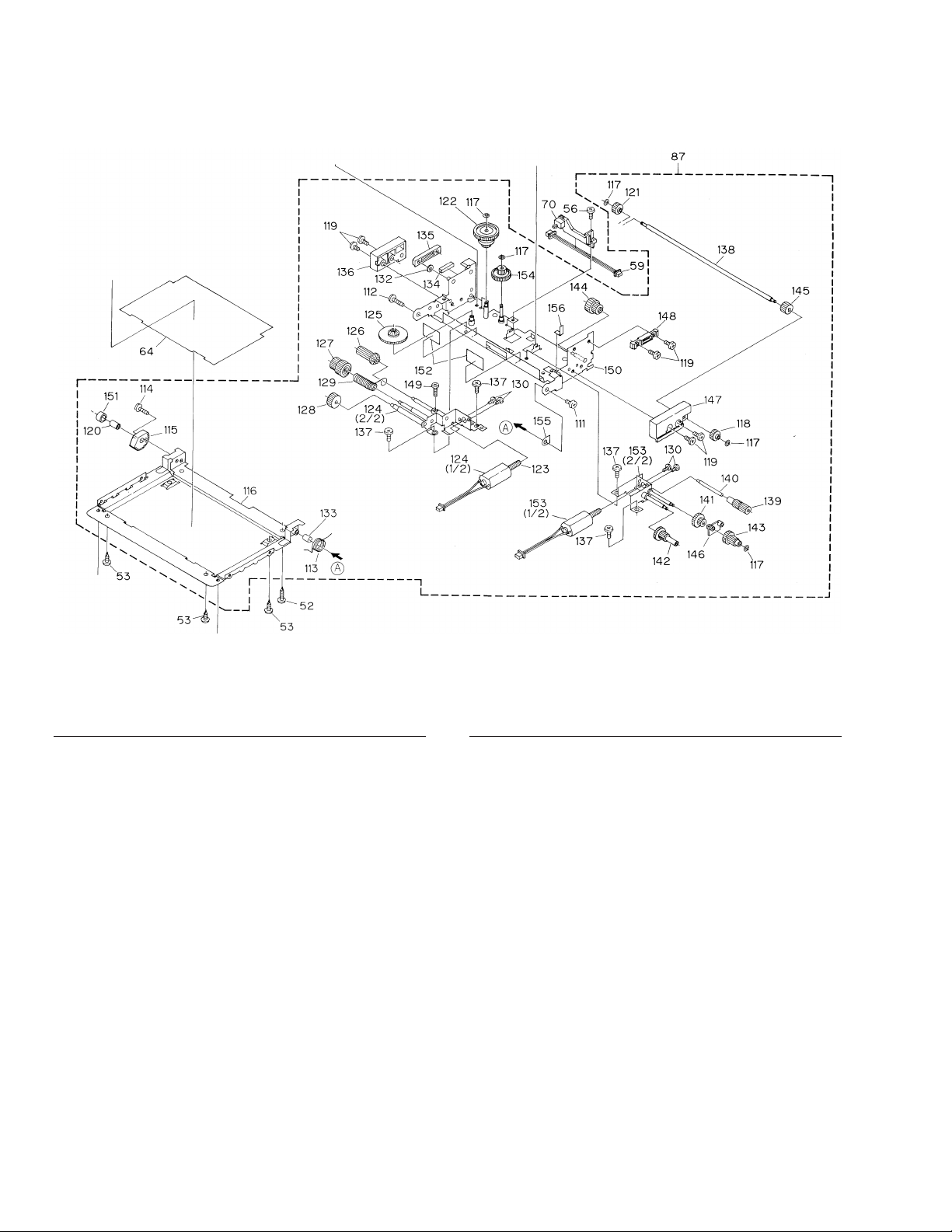
1. EXPLODED VIEWS AND PARTS LIST
111 ScrewM2X3 FB1521
112 ScrewM2X9 FB1523
113 Spring FS1573
114 ScrewM2X5.5 FB1522
115 Gear FH1267
116 Cover Unit(UC,EW model) FK1850
Cover Unit(ES model) FK1887
117 Washer FX1055
118 Gear 374K
119 ScrewM2.6X3.5 FB1520
120 Collar FH1268
121 Gear 374M
122 Torque Limiter 376F
123 Gear 376J
124 Motor Assy CXX1398
125 Gear 376T
126 Gear 376U
127 Gear 376V
128 Gear FH1266
129 Spring FS1574
130 ScrewM2X3 FB1031
132 Collar FX2631
133 Pipe FX2619
134 Cushion FX2483
135 Guide 377A
136 Guide 376Y
137 ScrewM2.6X2.5 FB1519
138 Shaft FD1233
139 Worm Wheel 373V
140 Gear Shaft FD1232
141 Gear 373W
142 Gear 374F
143 Gear 374G
144 Gear 374H
145 Gear 374J
146 Toe Gear 376W
147 Guide 376Z
148 Guide 376X
149 ScrewM1.7X6 FB1524
150 Try Assy FK1847
151 Spacer HF1282
152 Sheet FX2482
153 Motor Assy CXX1399
154 Worm Wheel 373T
155 Nonwoven Fabric FX2618
156 Sheet FX2594
1.1 DRIVE MECHANISM UNIT
- DRIVE MECHANISM UNIT SECTION PARTS LIST
Mark No. Description Part No. MarkNo.Description Part No.
Page 3
3
AVX-P7000CD,AVX-7000
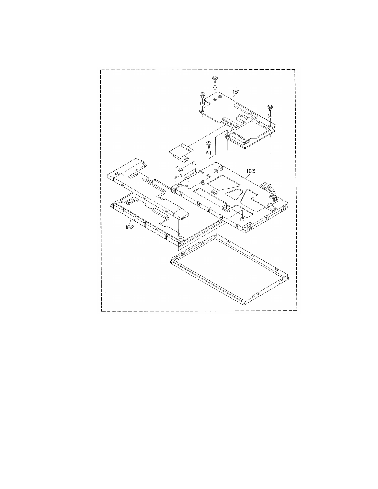
1.2 LCD MODULE
181 Video Unit NMP70-8398-112
182 TFT-LCD Module TFD70W14A
183 B/L Unit NMP75-8376-211
- LCD MODULE SECTION PARTS LIST
Mark No. Description Part No.
Page 4
4
AVX-P7000CD,AVX-7000
1
23
4
1
234
D
C
B
A
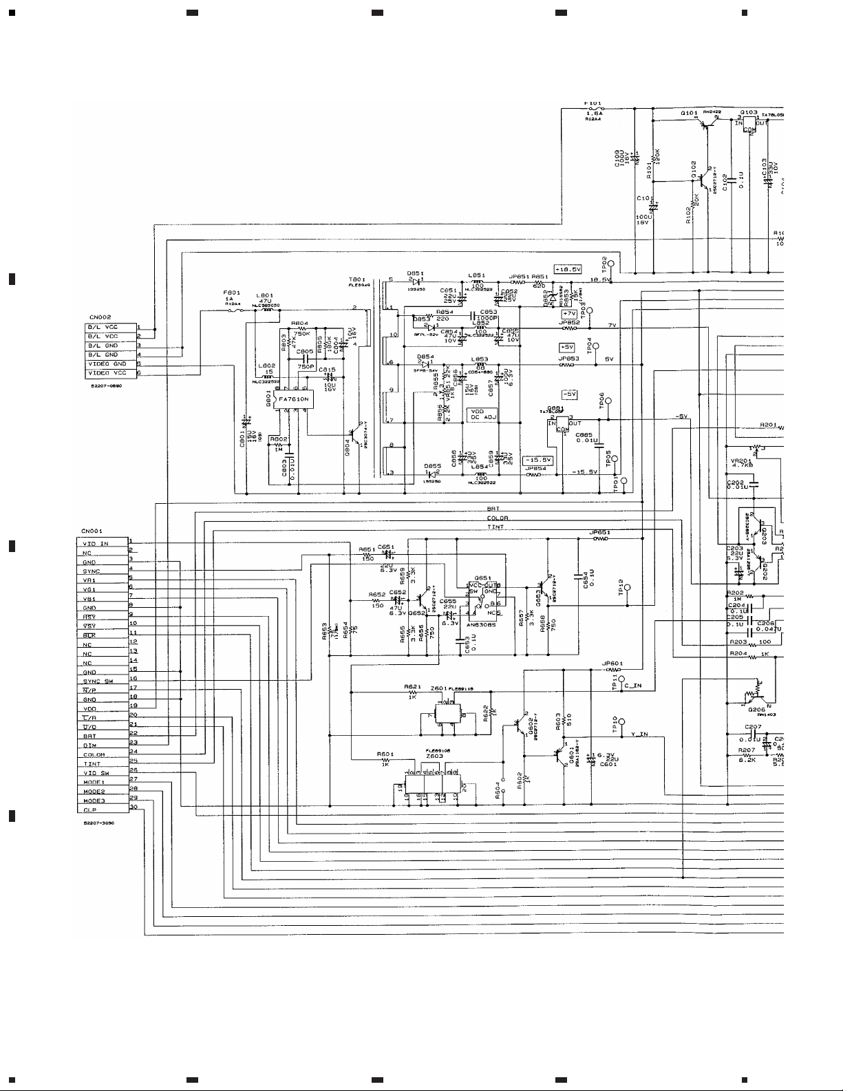
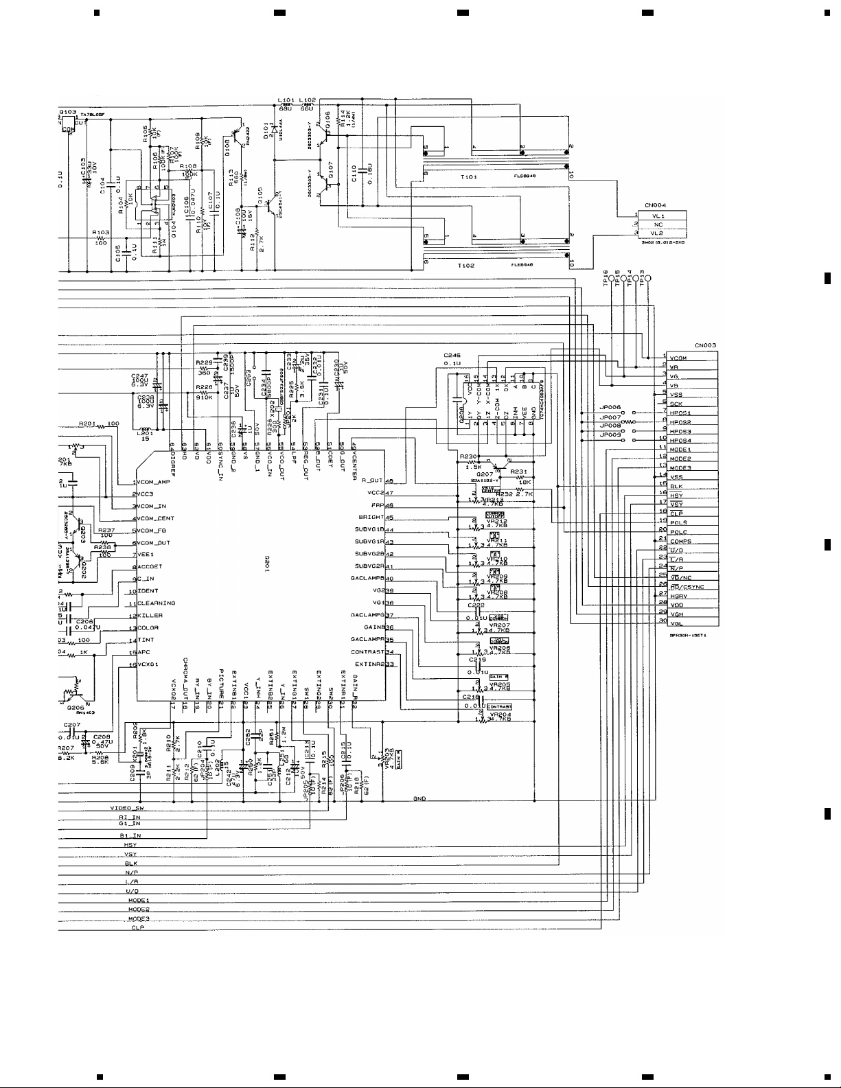
2. SCHEMATIC DIAGRAM
2.1 VIDEO UNIT
Page 5
5
AVX-P7000CD,AVX-7000
5
6
78
5
6
78
D
C
B
A
Page 6

6
AVX-P7000CD,AVX-7000
1
23
4
1
234
D
C
B
A
3. PCB CONNECTION DIAGRAM
3.1 VIDEO UNIT
IC,Q
Q881
Q801 Q206
Q201 Q202
Q203
Q601
Q107 Q106
Q602
Q804 Q201
Q105 Q208
Q104
Q108
Q103
Q653
Q652
Q102
Q651
Q101
Page 7

7
AVX-P7000CD,AVX-7000
5
6
78
5
6
78
D
C
B
A
NOTE FOR PCB DIAGRAMS
1. The parts mounted on this PCB
include all necessary parts for
several destination.
For further information for
respective destinations, be sure
to check with the schematic diagram.
2. Viewpoint of PCB diagrams
Capacitor
Connector
P.C.Board
Chip Part
SIDE A
SIDE B
SIDE A
Page 8

8
AVX-P7000CD,AVX-7000
1
23
4
1
234
D
C
B
A
Page 9

9
AVX-P7000CD,AVX-7000
5
6
78
5
6
78
D
C
B
A
SIDE B
Page 10

10
AVX-P7000CD,AVX-7000
Unit Number :
Unit Name : Video Unit
MISCELLANEOUS
Q 101 RN2422
Q 102 2SC2712-Y
Q 103 TA78L05F
Q 104 NJM2403M
Q 105 2SC4541-Y
Q 106 2SC3303-Y
Q 107 2SC3303-Y
Q 108 RN2422
Q 201 NJW1300A
Q 202 2SA1298-Y
Q 203 2SC3265-Y
Q 206 RN1403
Q 207 2SA1162-Y
Q 208 TC74HC4053AFS
Q 601 2SA1162-Y
Q 602 2SC2712-Y
Q 651 AN6308S
Q 652 2SC2712-Y
Q 653 2SC2712-Y
Q 801 FA7610N
Q 804 2SC3074-Y
Q 881 TA79L05F
D 101
D 851
D 852
D 853
D 854
D 855 1SS250
F 101
F 801 CEK1173
L 101
L 102
L 201 LCTA150J3225
L 202 LCTA150J3225
L 251
L 801
L 802 LCTA150J3225
L 851 LCTA101J3225
L 852 LCTA101J3225
L 853
L 854 LCTA101J3225
T 101 FLE6948
T 102 FLE6948
T 801 FLE6949
VR 201
VR 203
VR 204
VR 205
VR 206
VR 207
VR 208
VR 209
VR 210
VR 211
VR 212
VR 213
VR 851
X 201 NR18-GW3.58
X 202 CSBF503JF502
Z 601 FLE6911B
Z 603 FLE6910B
JP 006 RS1/16S0R0J
JP 007 RS1/16S0R0J
JP 008 RS1/16S0R0J
JP 009 RS1/16S0R0J
JP 201 RS1/16S202J
JP 204 RS1/16S10R0F
JP 205 RS1/16S10R0F
JP 206 RS1/16S10R0F
JP 601 RS1/16S0R0J
JP 602 RS1/16S0R0J
JP 651 RS1/16S0R0J
JP 851 RS1/16S0R0J
JP 852 RS1/16S0R0J
JP 853 RS1/16S0R0J
JP 854 RS1/16S0R0J
CN 001
CN 002
CN 003
CN 004
RESISTORS
R 101 RS1/16S124J
R 102 RS1/16S203J
R 103 RS1/16S101J
R 104 RS1/16S103J
R 105 RS1/16S1002F
R 106 RS1/16S1003F
R 107 RS1/16S1003F
R 108 RS1/16S1003F
R 109 RS1/16S1002F
R 110 RS1/16S1002F
5. ELECTRICAL PARTS LIST
NOTE:
- Parts whose parts numbers are omitted are subject to being not supplied.
- The part numbers shown below indicate chip components.
Chip Resistor
RS1/_S___J,RS1/__S___J
Chip Capacitor (except for CQS.....)
CKS....., CCS....., CSZS.....
=====Circuit Symbol and No.===Part Name Part No.
--- ------ ------------------------------------------ -------------------------
=====Circuit Symbol and No.===Part Name Part No.
--- ------ ------------------------------------------ -------------------------
Page 11

11
AVX-P7000CD,AVX-7000
R 111 RS1/16S105J
R 112 RS1/16S272J
R 113 RS1/8S561J
R 114 RS1/4S122J
R 201 RS1/16S101J
R 202 RS1/16S105J
R 203 RS1/16S101J
R 204 RS1/16S102J
R 207 RS1/16S822J
R 208 RS1/16S562J
R 209 RS1/16S182J
R 210 RS1/16S272J
R 211 RS1/16S222J
R 212 RS1/16S62R0F
R 214 RS1/16S62R0F
R 215 RS1/16S101J
R 218 RS1/16S62R0F
R 225 RS1/16S472J
R 226 RS1/16S301J
R 228 RS1/16S911J
R 229 RS1/16S361J
R 230 RS1/16S152J
R 231 RS1/16S183J
R 232 RS1/16S272J
R 237 RS1/16S101J
R 238 RS1/16S101J
R 250 RS1/16S122J
R 251 RS1/16S105J
R 601 RS1/16S102J
R 602 RS1/16S102J
R 603 RS1/16S511J
R 604 RS1/16S102J
R 621 RS1/16S102J
R 622 RS1/16S102J
R 651 RS1/16S151J
R 652 RS1/16S151J
R 653 RS1/16S750J
R 654 RS1/16S750J
R 655 RS1/16S332J
R 656 RS1/16S751J
R 657 RS1/16S332J
R 658 RS1/16S751J
R 659 RS1/16S332J
R 802 RS1/16S105J
R 803 RS1/16S473J
R 804 RS1/16S754J
R 805 RS1/16S184J
R 851 RS1/16S621J
R 853 RS1/16S153J
R 854 RS1/16S221J
R 855 RS1/16S223J
R 856 RS1/16S222J
CAPACITORS
C 101 CEHV101M16
C 102 CKSRYF104Z25
C 103 CEHV330M10
C 104 CKSRYF104Z25
C 105 CKSRYF104Z25
C 106 CKSRYB473K16
C 107 CKSRYF104Z25
C 108 CEHV100M16
C 109 CEHV101M16
C 110
C 202 CKSRYB103K50
C 203
C 204 CKSRYF104Z25
C 205 CKSRYF104Z25
C 206 CKSRYB473K16
C 207 CKSRYB103K50
C 208 CEHV4R7M50
C 209 CCSRCH030C50
C 210 CKSRYF104Z25
C 212 CEHV1R0M50
C 213 CKSRYF104Z25
C 215 CKSRYF104Z25
C 218 CKSRYB103K50
C 219 CKSRYB103K50
C 222 CKSRYB103K50
C 230 CEHV1R0M50
C 231 CKSRYF104Z25
C 232 CKSRYB103K25
C 233 CEHV2R2M50
C 234 CKSRYB682K50
C 236 CEHV1R0M50
C 237 CEHV1R0M50
C 238 CEHV101M6R3
C 239 CKSRYB152K50
C 242 CEHV470M6R3
C 246 CKSRYF104Z25
C 247 CEHV101M6R3
C 251 CCSRCH220J50
C 252 CCSRCH220J50
C 253
C 601 CEHV220M6R3
C 651 CEHV220M6R3
C 652 CEHV470M6R3
C 653 CKSRYF104Z25
C 654 CKSRYF104Z25
C 655 CEHV220M6R3
C 801
C 803 CKSRYB103K50
C 804
C 805 CCSRCH751J25
C 815
C 851
C 852
C 853 CKSRYB102K50
C 854
C 855
C 856
C 857
C 858
C 859
C 885 CKSRYB103K50
=====Circuit Symbol and No.===Part Name Part No.
--- ------ ------------------------------------------ -------------------------
=====Circuit Symbol and No.===Part Name Part No.
--- ------ ------------------------------------------ -------------------------
1st production Running change
(TFD70W14-MM1) (TFD70W14-MM2)
HPOS JP007: 0Ω Resistor JP008:0Ω Resistor
(HPOS2=Hi) (HPOS3=Hi)
Page 12

12
AVX-P7000CD,AVX-7000
5. GENERAL INFORMATION
5.1 DISASSEMBLY
- Removing the Back Light Unit
1. Remove the four screws.
2. Disconnect the two connectors.
3. Remove the rear shield and front shield.
4. Disconnect the connector and remove the PCB.
5. Remove the TFD-LCD Module.
Front Shield
Rear Shield
PCB
TFD-LCD Module
Back Light Unit
Page 13

13
AVX-P7000CD,AVX-7000
- CWX2389 LCD module troubleshooting
No images with the
composite signal
1No images with the composite signal
Back light turns ON?
Circuit current flows normally?
Video signal is obtained at R654 (75 ohms)?
Video signal is obtained at Q653 (TR)?
Chroma signal is obtained at
Pin-9 of Q201 (NJW1300A)?
Y-signal is obtained at Pin24 of Q201 (NJW1300A)?
5V is obtained at Pin-23 and Pin-61 of Q201 (NJW1300A)?
7V is obtained at Pin-2 of Q201 (NJW1300A)?
POLC signal is obtained at Pin-46
of Q201 (NJW1300A)?
Sync pulses in synchronization with the input signal are
obtained at Pin-62 and Pin-63 of Q201 (NJW1300A)?
(-5)V is obtained at Pin-7
of Q201 (NJW1300A)?
Normal V-COM signal is obtained at TP13?
Go to Item 2 Back light doesn't turn ON.
Go to Item3 No power.
Check the input connecting flexible cables and its periphery.
Check Sync SW (Q651) and its periphery.
Check Delay line (Z601) and its periphery.
Go to Item3 No power.
Check CN003 (30-pin flexible connector) and its periphery.
Go to Item4 Out of Sync
Go to Item3 No power.
Check Q202, Q203 (Buffer), and their periphery.
Check Delay line (Z603) and its periphery.
NO
NO
YES
NO
Page 14

14
AVX-P7000CD,AVX-7000
RGB signal for LCD is obtained at Pin-48,
Pin-50, and Pin-52 of Q201 (NJW1300A)?
Replace Q201 (NJW1300A).
Blanking (BLK) signal is obtained at
Pin-9 to Pin-11 of Q208 (74HC4053)?
RGB signal for LCD is obtained at Pin-2 to
Pin-4 of CN003 (30-pin flexible connector)?
Normal signal is obtained at each terminals of CN003?
Replace LCD module.
Check CN003 (30-pin flexible connector) and its periphery.
Check Q208 (74HC4053) and its periphery.
Check CN003 (30-pin flexible connector) and its periphery.
2Back light doesn't turn ON.
F101 (fuse) is broken out? Replace F101.
NO
NO
Back light doesn't turn ON.
Dimmer voltage (1.35V to 3.9V) is
obtained at pin-2 of Q104 (NJM2403)?
At Dimmer mode, triangular waves are
obtained at Pin-6 of Q104 (NJM2403)?
At Dimmer mode, 0/5V rectangular
waves are obtained at Q108 (TR)?
At 100% dimmer mode, ON voltage (about
0.7V) is obtained at the base of Q105 (TR)?
Half-wave oscillating waveform is obtained at
both ends of C110 (film capacitor)?
High voltage is obtained at pin-1 and Pin-3 of CN004?
Check CN004 and replace back light.
Check Q103 (3-terminal regulator) and its periphery.
Check Q104 (NJM2403) and its periphery.
Check input flexible cables and their periphery.
Check Q104 (NJM2403) and its periphery.
5V is obtained at Pin-8 of Q104 (NJM2403)?
Check Q105, Q108, and their periphery.
Check the primary windings of Inverter transformer.
Replace T101 and T102 (Inverter transformer).
YES
NO
YES
NO
Page 15

15
AVX-P7000CD,AVX-7000
3No power
F801 (fuse) is broken out? Replace F801.
NO
NO
No power
18.5V is obtained at TP02? If not, the resistance
between TP02 and GND is 100k ohms or more?
7V is obtained at TP03? if not, the resistance
between TP03 and GND is 500 ohms or more?
5V is obtained at TP04? If not, the resistance
between TP04 and GND is 35 ohms or more?
(-15.5)V is obtained at TP05? If not, the resistance
between TP05 and GND is 950 ohms or more?
(-5)V is obtained at TP06? If not, the resistance
between TP06 and GND is 400 ohms or more?
Input voltage 9V is obtained at
Pin-5 of Q801 (FA7610N)?
Triangular waves are obtained at
Pin-6 of Q801 (FA7610N)?
Switching waves are obtained at Q804 (TR)?
Check Transformer (T801) and replace it.
Check 18.5V line to remove short-circuits. (CN003 and its periphery)
Check 7V line to remove short-circuits.
(Q201, Q202, Q203, and their periphery)
Check 5V line to remove short-circuits.
(Q201, Q208, Q651, and their periphery)
Check (-15.5)V line to remove short-circuits.
(Q881, CN003, and their periphery)
Check (-5)V line to remove short-circuits.
(Q201, Q202, Q203, and their periphery)
Check F801, input flexible cables, and their periphery.
Check Q801 and its periphery.
Go to item3 No power.
4Out of Sync
Video signal is obtained at Q653 (TR)? Check input flexible cables, Q651, and their periphery.
YES
NO
Out of Sync
Video signal is obtained at Pin-60
of Q201 (NJW1300A)?
Full-wave oscillating waveform is obtained at
Pin-55 and Pin-56 of Q201 (NJW1300A)?
5V is obtained at Pin-61 of
Q201 (NJW1300A)?
Check R229 (LPF, 360 ohms) and its periphery.
Check X202 (Ceramic resonator) and its periphery.
Check Q801 and its periphery.
YES
NO
Page 16

AVX-P7000CD,AVX-7000
Video signal is obtained at Q653 (TR)?
Chroma signal is obtained at
Pin-9 of Q201 (NJW1300A)?
X'tal oscillating waves are obtained at Pin-16
and Pin-17 of Q201 (NJW1300A)?
Sync pulses in synchronization with Input signal are
obtained at Pin-62 and Pin-63 of Q201 (NJW1300A)?
Check CN003 and LCD.
Check Z601 (delay line) and its periphery.
Check X201 (X'tal) and its periphery.
Check Q201 (NJW1300A) and replace it.
5No color with Composite signal
NO
NO
No color with composite signal
Chroma signal is obtained at Pin18 of Q201 (NJW1300A)?
Check Q201 (NJW1300A) and replace it.
Check input flexible cables, Q651 and their periphery.
Check Pin-12 to Pin-15 of
Q201 (NJW1300A).
YES
NO
YES
NO
 Loading...