

Page 1
PIONEER CORPORATION 4-1, Meguro 1-chome, Meguro-ku, Tokyo 153-8654, Japan
PIONEER ELECTRONICS (USA) INC. P.O. Box 1760, Long Beach, CA 90801-1760, U.S.A.
PIONEER EUROPE NV Haven 1087, Keetberglaan 1, 9120 Melsele, Belgium
PIONEER ELECTRONICS ASIACENTRE PTE. LTD. 253 Alexandra Road, #04-01, Singapore 159936
PIONEER CORPORATION 2002
ORDER NO.
CRT2876
AVR-W6100/UC
OVERHEAD DISPLAY
AVR-W6100
OVERHEAD DISPLAY
AVR-W6100
EW
UC
For details, refer to "Important symbols for good services".
K-ZZS.MAY 2002.printed in Japan
Page 2
f
1234
SAFETY INFORMATION
UC model
CAUTION
A
This service manual is intended for qualified service technicians; it is not meant for the casual do-it-yourselfer.
Qualified technicians have the necessary test equipment and tools, and have been trained to properly and safely repair
complex products such as those covered by this manual.
Improperly performed repairs can adversely affect the safety and reliability of the product and may void the warranty.
If you are not qualified to perform the repair of this product properly and safely, you should not risk trying to do so
and refer the repair to a qualified service technician.
WARNING
This product
California to cause cancer, birth defects or other reproductive harm.
Health & Safety Code Section 25249.6 - Proposition 65
contains lead in solder and certain electrical parts contain chemicals which are known to the state o
EW model
B
Danger of explosion if battery is incorrectly replaced.
Replaced only with the same or equivalent type recommended by the manufacture.
Discord used batteries according to the manufacture's instructions.
[ Important symbols for good services ]
In this manual, the symbols shown-below indicate that adjustments, settings or cleaning should be made securely.
When you find the procedures bearing any of the symbols, be sure to fulfill them:
1. Product safety
You should conform to the regulations governing the product (safety, radio and noise, and other regulations), and
should keep the safety during servicing by following the safety instructions described in this manual.
2. Adjustments
To keep the original performances of the product, optimum adjustments or specification confirmation is indispensable.
C
In accordance with the procedures or instructions described in this manual, adjustments should be performed.
CAUTION
3. Cleaning
For optical pickups, tape-deck heads, lenses and mirrors used in projection monitors, and other parts requiring cleaning,
proper cleaning should be performed to restore their performances.
4. Shipping mode and shipping screws
To protect the product from damages or failures that may be caused during transit, the shipping mode should be set or
the shipping screws should be installed before shipping out in accordance with this manual, if necessary.
5. Lubricants, glues, and replacement parts
D
2
Appropriately applying grease or glue can maintain the product performances. But improper lubrication or applying
glue may lead to failures or troubles in the product. By following the instructions in this manual, be sure to apply the
prescribed grease or glue to proper portions by the appropriate amount.For replacement parts or tools, the prescribed
ones should be used.
AVR-W6100/UC
1234
Page 3

A
B
5678
CONTENTS
SAFETY INFORMATION. . . . . . . . . . . . . . . . . . . . . . . . . . . . . . . . . . . . . 2
1. SPECIFICATIONS . . . . . . . . . . . . . . . . . . . . . . . . . . . . . . . . . . . . . . . 4
2. EXPLODED VIEWS AND PARTS LIST . . . . . . . . . . . . . . . . . . . . . . . . . . . . 6
2.1 PACKING . . . . . . . . . . . . . . . . . . . . . . . . . . . . . . . . . . . . . . . . . 6
2.2 EXTERIOR . . . . . . . . . . . . . . . . . . . . . . . . . . . . . . . . . . . . . . . . 8
3. BLOCK DIAGRAM AND SCHEMATIC DIAGRAM . . . . . . . . . . . . . . . . . . . . . . .10
3.1 BLOCK DIAGRAM. . . . . . . . . . . . . . . . . . . . . . . . . . . . . . . . . . . . .10
3.2 OVERALL CONNECTION DIAGRAM . . . . . . . . . . . . . . . . . . . . . . . . . . .12
3.3 MOTHER PCB(GUIDE PAGE). . . . . . . . . . . . . . . . . . . . . . . . . . . . . . .14
3.4 IR PCB,RCA PCB . . . . . . . . . . . . . . . . . . . . . . . . . . . . . . . . . . . . .20
3.5 MONITOR UNIT . . . . . . . . . . . . . . . . . . . . . . . . . . . . . . . . . . . . . .22
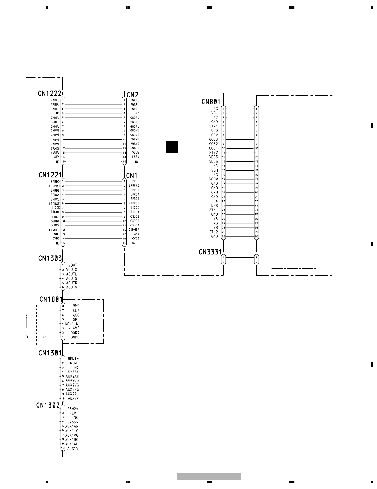
4. PCB CONNECTION DIAGRAM . . . . . . . . . . . . . . . . . . . . . . . . . . . . . . . .28
4.1 MOTHER PCB. . . . . . . . . . . . . . . . . . . . . . . . . . . . . . . . . . . . . . .28
4.2 IR PCB. . . . . . . . . . . . . . . . . . . . . . . . . . . . . . . . . . . . . . . . . . .30
4.3 MONITOR UNIT . . . . . . . . . . . . . . . . . . . . . . . . . . . . . . . . . . . . . .32
4.4 RCA PCB . . . . . . . . . . . . . . . . . . . . . . . . . . . . . . . . . . . . . . . . .34
5. ELECTRICAL PARTS LIST . . . . . . . . . . . . . . . . . . . . . . . . . . . . . . . . . .35
6. ADJUSTMENT. . . . . . . . . . . . . . . . . . . . . . . . . . . . . . . . . . . . . . . . .45
6.1 MOTHER PCB ADJUSTMENT . . . . . . . . . . . . . . . . . . . . . . . . . . . . . .46
6.2 IR PCB ADJUSTMENT . . . . . . . . . . . . . . . . . . . . . . . . . . . . . . . . . .48
6.3 MONITOR SECTION ADJUSTMENT . . . . . . . . . . . . . . . . . . . . . . . . . . .50
6.4 EEPROM SETTING MODE . . . . . . . . . . . . . . . . . . . . . . . . . . . . . . . .54
7. GENERAL INFORMATION . . . . . . . . . . . . . . . . . . . . . . . . . . . . . . . . . .57
7.1 DIAGNOSIS . . . . . . . . . . . . . . . . . . . . . . . . . . . . . . . . . . . . . . . .57
7.1.1 DISASSEMBLY . . . . . . . . . . . . . . . . . . . . . . . . . . . . . . . . . . . . .57
7.1.2 CONNECTOR FUNCTION DESCRIPTION . . . . . . . . . . . . . . . . . . . . . . .59
7.2 IC . . . . . . . . . . . . . . . . . . . . . . . . . . . . . . . . . . . . . . . . . . . . .60
7.3 OPERATIONAL FLOW CHART . . . . . . . . . . . . . . . . . . . . . . . . . . . . . .68
8. OPERATIONS . . . . . . . . . . . . . . . . . . . . . . . . . . . . . . . . . . . . . . . . .69
AVR-W6100/UC
56
C
D
7
3
8
Page 4

1234
1. SPECIFICATIONS
AVR-W6100/UC
General
Power source ...................................................................... 14.4 V DC (10.8 — 15.1 V allowed)
Grounding system ................................................................ Negative type
A
Max. current consumption .................................................. 3 A
Backup current .................................................................... Less than 1 mA
Display Unit
Screen size/Aspect ratio ...................................................... 6.5 inch wide/16:9
Pixels .................................................................................... 336,960 (1,440 × 234)
Type .................................................................................... TFT active matrix, transmissive type
Color system ........................................................................ NTSC
Operating temperature range .............................................. –10 — +50 °C [+14 to +122 °F ]
Storage temperature range .................................................. –40 — +80 °C [-40 to +176 °F ]
Angle adjustment
Flip angle ........................................................................ 0 — 105 °
Swivel ............................................................................ 25 ° (R) — 25 ° (L)
Dimensions .......................................................................... 260 (W) ×50 (H) × 220 (D) mm
Display ................................................................................ 105 (W) × 25 (H) × 180 (D) mm
Weight ................................................................................ 1.1 kg [2.4 lbs]
B
(effective display area: 154× 87 mm)
[ 6-1/8 × 3-3/8 in. ]
[ 10-1/4(W) × 2(Η) × 8-5/8(D) in. ]
[ 4-1/8(W) × 1(Η) × 7-1/8(D) in. ]
AVR-W6100/EW
General
Power source ...................................................................... 14.4 V DC (10.8 — 15.1 V allowed)
Grounding system ................................................................ Negative type
Max. current consumption .................................................. 3 A
Backup current .................................................................... Less than 1 mA
Display Unit
Screen size/Aspect ratio ...................................................... 6.5 inch wide/16:9
Pixels .................................................................................... 336,960 (1,440 × 234)
Type .................................................................................... TFT active matrix, transmissive type
Color system ........................................................................ NTSC/PAL compatible
Operating temperature range .............................................. –10 — +50 °C
Storage temperature range .................................................. –40 — +80 °C
Angle adjustment
C
Flip angle ........................................................................ 0 — 105 °
Swivel ............................................................................ 25 ° (R) — 25 ° (L)
Dimensions .......................................................................... 260 (W) ×50 (H) × 220 (D) mm
Display ................................................................................ 105 (W) × 25 (H) × 180 (D) mm
Weight ................................................................................ 1.1 kg
(effective display area: 154× 87 mm)
D
4
1234
AVR-W6100/UC
Page 5

A
B
5
5678
C
AVR-W6100/UC
56
D
7
8
Page 6
1234
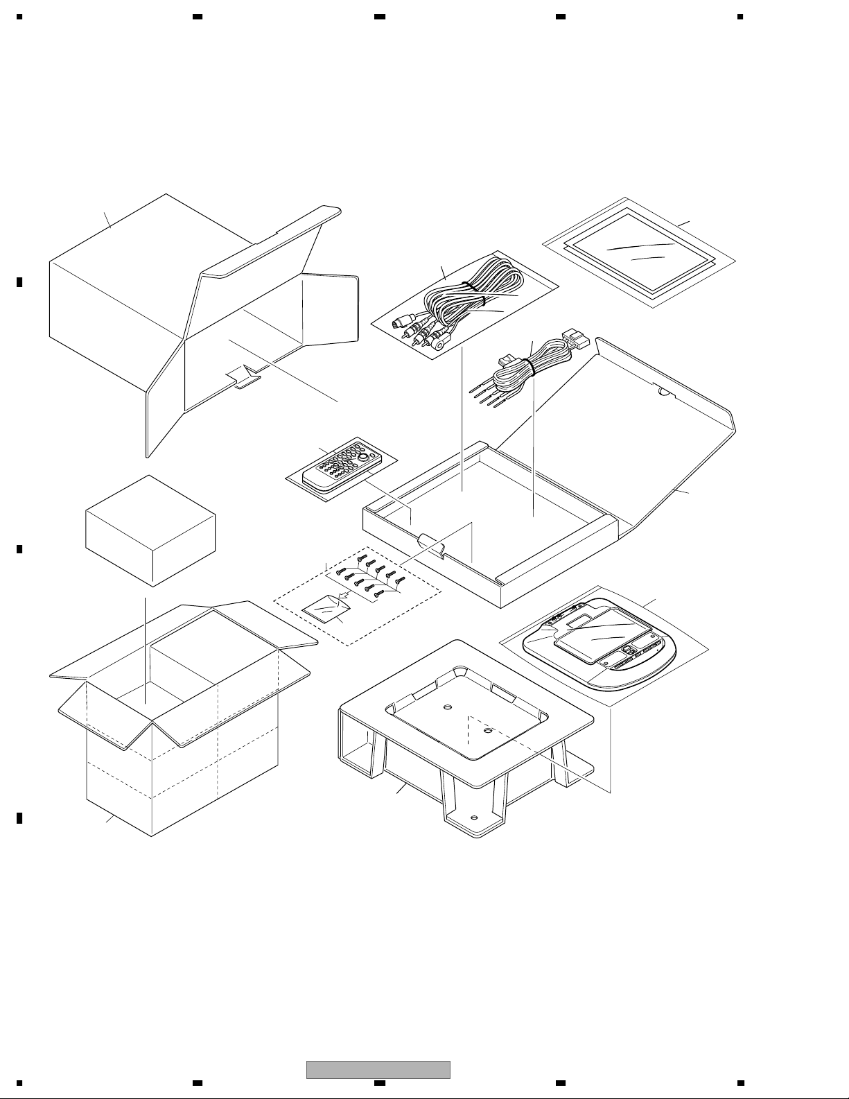
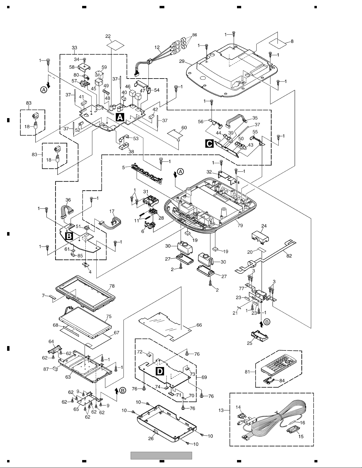
2. EXPLODED VIEWS AND PARTS LIST
NOTES : • Parts marked by " * " are generally unavailable because they are not in our Master Spare Parts List.
• Screw adjacent to mark on the product are used for disassembly.
• For the applying amount of lobricants or glue, follow the instructions in this manual.
A
(In the case of no amount instructions,apply as you think it appropriate.)
"
2.1 PACKING
12
5
4
B
3
1
11
6
7
10
8
C
2
9
D
6
1234
AVR-W6100/UC
Page 7
A
B
5678
(1) PACKING SECTION PARTS LIST
Mark
No. Description Part No.
* 1-1 Card See Contrast table(2)
1-2 Owner's Manual See Contrast table(2)
1-3 Owner's Manual See Contrast table(2)
1-4 Polyethylene Bag CEG1116
* 1-5 Warranty Card See Contrast table(2)
2 Protector CHP2567
3 Remote Control Assy CXB9056
4 Cord Assy CDE6979
5 Cord Assy CDE7013
Mark No. Description Part No.
6 Screw Assy CEA3252
7 Screw BPZ26P100FMC
* 8 Polyethylene Bag E36-613
9 Contain Box See Contrast table(2)
10 Polyethylene Bag See Contrast table(2)
11 Sub Carton CHG4722
12 Carton See Contrast table(2)
(2) CONTRAST TABLE
AVR-W6100/UC, and AVR-W6100/EW are constructed the same except for the following:
k NO Symbol and Description AVR-W6100/UC AVR-W6100/EW
Mar
* 1-1 Card ARY1048 Not used
1-2 Owner's Manual CRD3660 CRD3643
1-3 Owner's Manual Not used CRD3644
* 1-5 Warranty Card Not used CRY1157
9 Contain Box CHL4720 CHL4721
10 Polyethylene Bag CEG1185 CEG1042
12 Carton CHG4720 CHG4721
Owner's Manual,Installation Manual
Part No. Language
CRD3643 English, Spanish, German
CRD3644 French, Italian, Dutch
CRD3660 English, French, Spanish
C
AVR-W6100/UC
56
D
7
7
8
Page 8
1234
2.2 EXTERIOR
A
B
C
D
8
1234
AVR-W6100/UC
Page 9

A
B
5678
EXTERIOR SECTION PARTS LIST
Mark
No. Description Part No.
1 Screw BPZ26P080FMC
2 Screw BPZ30P100FNI
3 Screw BPZ30P100FZK
4 Knob(LAMP) CAA2728
5 Button CAC7558
6 Button(OPEN) CAC7559
* 7 Badge CAH1754
* 8 Label(AVR-W6100/UC) CAN1478
9 Screw(M2.6x4) CBA1156
10 Screw(M2x6) CBA1594
11 Spring CBH2579
12 Cord Assy CDE5901
13 Cord Assy CDE6979
14 Fuse(4A) CEK1001
15 Cap CNS1472
16 Resistor RS1/2P102JL
17 Cord Assy CDE7068
18 Lamp(IL1801,1802) CEL1735
19 Cushion CNM8065
20 Spacer CNM7918
21 Spacer CNM7919
22 Spacer CNM7920
23 Spacer CNM8009
24 Cover CNS7038
25 Cover CNS7039
26 Case CNS7042
27 Plate CNS7043
28 Lever CNV7139
29 Cover CNV7140
30 Reflector CNV7142
31 Cover CNV7188
32 Cover CNV7191
33 Mother Unit(UC model) CWM8247
Mother Unit(EW model) CWM8250
34 Screw BMZ30P080FMC
35 Cord Assy(CN1581) CDE6834
36 Cord Assy(CN1411) CDE7067
37 Clamper CEF1005
38 Plug(CN1801) CKM1135
39 Pin Jack(CN1582) CKS1825
40 Connector(CN1371) CKS3232
41 Connector(CN1501) CKS3235
42 Connector(CN1303) CKS3586
43 Connector(CN1584) CKS4124
44 Connector(CN1585) CKS4124
45 Connector(CN1201) CKS4598
46 Connector(CN1301) CKS4599
47 Connector(CN1302) CKS4599
48 Connector(CN1221) CKS4600
49 Connector(CN1222) CKS4600
56
Mark
50 Pin Jack(CN1583) CKS4601
51 Connector(CN1591) CKS4633
52 Connector(CN1802) CKS4634
53 Bracket CNC5862
54 Holder CNC9877
55 Holder CNC9878
56 Holder CNC9879
57 Holder CNC9880
58 Heat Sink CNC9881
59 Holder CND1097
60 Insulator CNM7916
61 Cushion CNM8008
62 Screw(M2x2.5) CBA1371
63 Holder CND1072
64 Holder CND1073
65 Holder CND1074
66 Insulator CNM7678
67 Insulator CNM7742
68 Spacer CNM8010
69 Monitor Unit CWM8246
70 Terminal(CN802) CKF1064
71 Connector(CN801) CKS3991
72 Connector(CN3331) CKS4428
73 Connector(CN1) CKS4618
74 Connector(CN2) CKS4618
75 LCD Panel CWX2671
76 Screw IMS20P025FMC
77 Hinge Unit CXB8657
78 Grille Unit CXB8725
79 Grille Unit CXB8736
80 Transistor(Q1813) 2SD2375
81 Remote Control Assy CXB9056
82 PCB Unit CXB9066
83 Lamp CEL1714
84 Cover CZN5357
85 IC(IC1501) TSOP4840SB1
86 Cap CNV6727
87 Spacer CNM8064
AVR-W6100/UC
No. Description Part No.
7
C
D
9
8
Page 10
1234
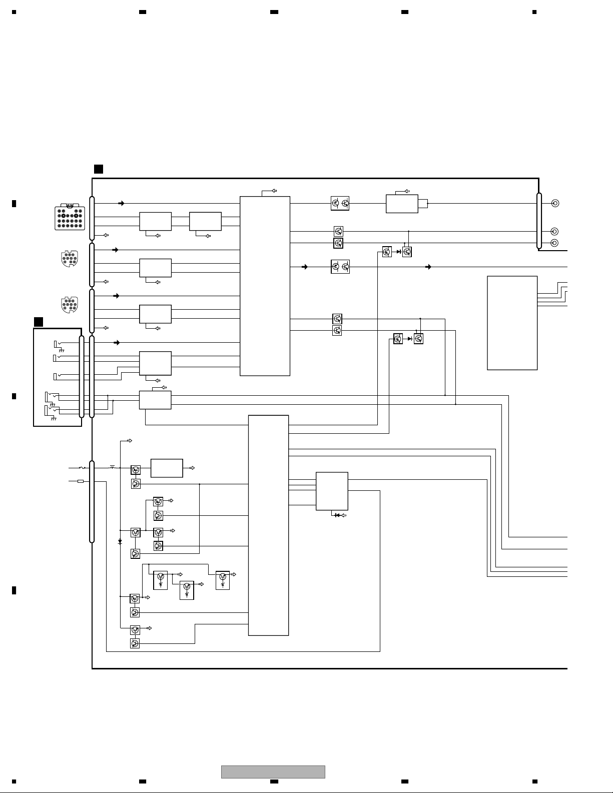
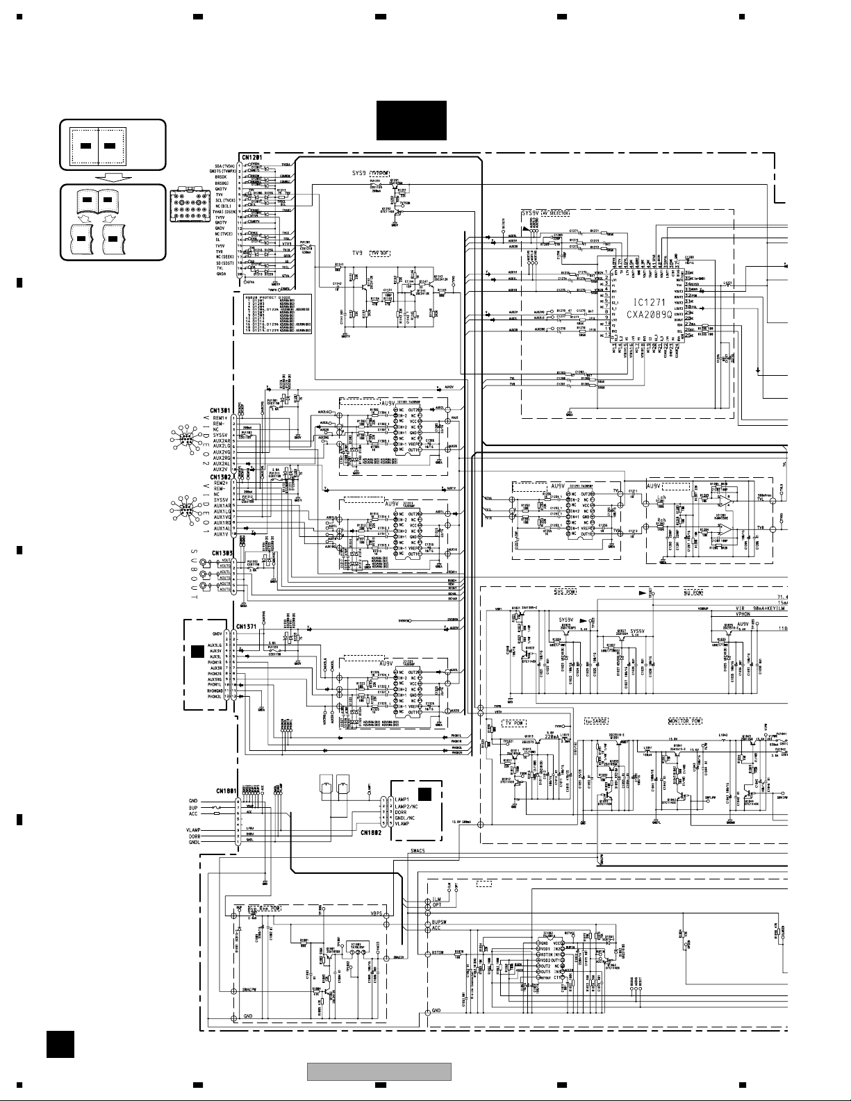
3. BLOCK DIAGRAM AND SCHEMATIC DIAGRAM
3.1 BLOCK DIAGRAM
A
MOTHER PCB
A
15
V3
16
LV3
18
RV3
8
V2
9
LV2
11
RV2
1
V1
2
LV1
4
RV1
47
TV
46
LTV
48
RTV
34
AV
SELECTOR
IC 1271
CXA2089Q
5
EVOL
65
SWACPW
20
MVIPW
SYSTEM
CONTROLLER
IC 1601(1/2)
PE5304B
21
MFLPW
VOUT1
LOUT1
ROUT1
VOUT2
LOUT2
ROUT2
MUTEB
MUTEA
KDT0
KDT1
RESET
BSENS
ASENS
VBUP5
40
39
41
33
30
32
35
36
78
79
60
62
63
68
AUX3V
AUX3L
AUX3R
BUP
ACC
CN1201
TVV
6
TVL
19
TVR
16
10
CN1301
AUX2V
10
AUX2AL
9
AUX2AR
5
4
CN1302
AUX1V
10
AUX1AL
9
AUX1AR
5
4
CN1311
AUX3V
4
4
AUX3L
5
5
3
3
AUX3R
7
7
9
9
1L
10
10
1R
6
6
2L
12
12
2R
8
8
CN1801
BUP
7
ACC
6
TV AUDIO ISOLATION
12 8
13 1
TV9V
AUX AUDIO2 ISOLATION
12 8
13 1
SYS5V
AUX AUDIO1 ISOLATION
12 8
13 1
SYS5V
AUX AUDIO3 ISOLATION
12 8
10
13
15
17 4
14
BUP
Q1801
Q1891
Q1893
IC 1251
TA2050F
6
IC 1301
TA2050F
6
IC 1311
TA2050F
6
IC 1321
TA2050F
6
15,16
IC 1371
TDA7496L
6
HEAD PHONE AMP
EVOL
REGULATOR
13
TA78L05F
Q1802
Q1843
Q1841
TV AUDIO AMP
57
IC 1201
31
NJM4558E
Q1844
VSWBUP
1
9
8
ACHAL
ACHAR
SWAC5V
PWRVI
PWRFL
VAU9V
VAU9V
VAU9V
VAU9V
IC 1801
Q1842
VAU9V
TO TUNER UNIT
VIDEO2
VIDEO1
B
RCA PCB
C
CN1581
PHONE1L
PHONE1R
PHONE2L
PHONE2R
C
VSYS9V
AV SELECTOR
AV SELECTOR
SENSE
7
IC 1861
5
PAJ001A
6
2
BUFFER
Q1264 Q1262
Q1131
BUFFER
Q1263 Q1261
Q1111
Q1112
14
BUFFER
Q1132
BUFFER
3
9
BUP
RSTSW
ACC
SYS5V
7
1
IC 1221
NJM2267M
MONITOR 75Ω DRIVE
MUTE
Q1133
Q1621
Q1113
Q1622
3
4
MUTE
SYSTEM
CONTROLLER
IC 1601(2/2)
PE5304B
CN1303
VOUT
AOUTL
AOUTR
OSDCS
OSDDT
OSDCK
DIMMER
1
3
5
14
12
13
6
Q1821
Q1813
Q1822
Q1812
Q1823
VSWBUP
TV9V
VSYS9V
Q1827
SYS5V
Q1835
VAU9V
66
SYSPW
64
TVPW
D
10
AVR-W6100/UC
1234
Page 11
A
B
5678
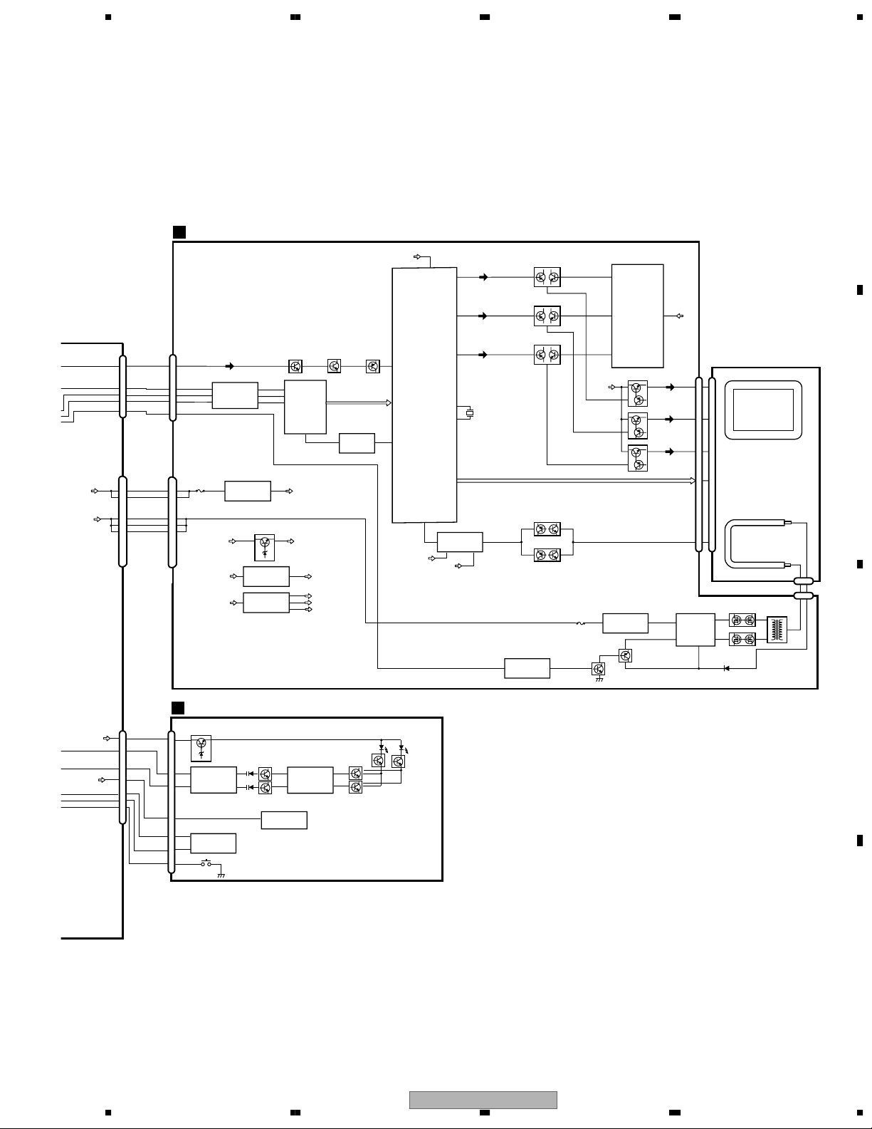
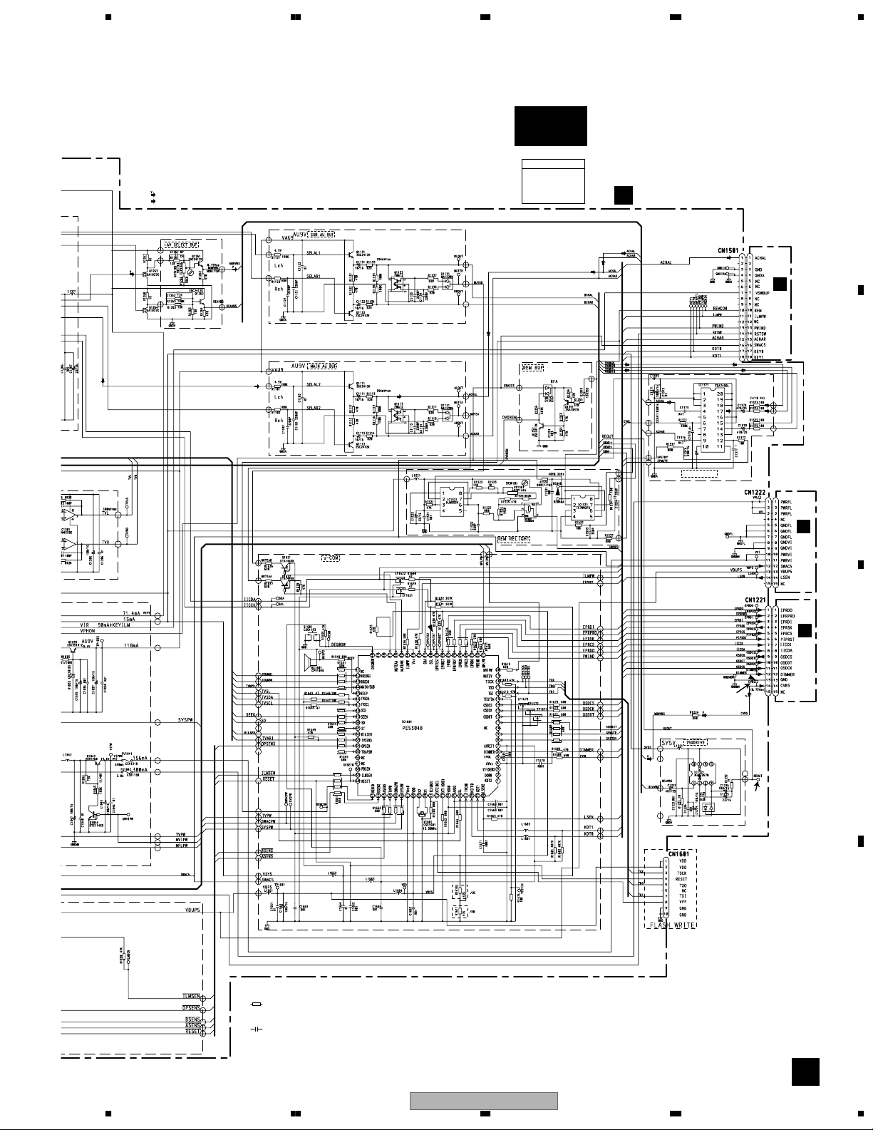
MONITOR UNIT
D
V25VCC
6,12
ROUT
Q153
RGB AMP
734
PWRVI
PWRFL
VSWBUP
SWAC5
CN1221
CN1222
PWRVI
PWRFL
CN1501
ACHAL
ACHAR
KEY0
KEY1
RSTSW
6
IC 901
NJM2903V
Q152
Q151
Q182
Q183
7
36 4
GOUT
CN1
14
9
10
11
12
10
11
1
2
3
CVBS
14
CSDCS
3
9
OSDDT
10
OSDCK
11
12
DIMMER
CN2
V14VCC
10
11
VFLVCC
1
2
3
6
TC7WH34FU
1
14.4V
2
V8VCC
V33VCC
V33VCC
IC82
LT1376CS8
5
2
7
IC 851
Q835
IC 841
2
R1130H251B
IC 861
4
MAX1748EUE
3
5
4
3
POWER SUPPLY
IR PCB
B
CN1411
7
1
15
16
17
18
14
Q1451
7
AMP AMP
9
1
IC1411
BA3308FV
13
15
16
17
KEY
MATRIX
18
14
S1531 RESET
Q1431
7
1
1
3
Q1441
REMOTE CONTROL SENSOR
3
IC1501
TSOP4840SB1
Q101
CSSIN
PD5582A
SCK
OSC1
1
V33VCC
V5VCC
1
15
7
8
TC7W04FU
OSD
IC 601
IC1471
V25VCC
V8VCC
V18VCC
VM12VCC
Q103
4
7
5
R,G,B
IC 92
TC7S08FU
Q1481
Q1482
Q1491
Q102
65
CVI1
1
SCKE
101
2 SCREEN IC
IC 1
TC90A64AF
POLC
28
6
V8VCC
VM12VCC
Q1492
BOUT
82
X0
X1
83
VCOM AMP
IC 181
NJM082BV
8
X1
42MHz
1
4
1
1438
V8VCC
FU3311
3 1 5,14,15
Q3331
IC 151
NJM2138V
Q156
Q155
Q154
INVERTER FOR BACK LIGHT
IC 3332
TA78L05F
Q3332
CN801
7
V8VCC
VR
VG
VB
VCOM
IC 3331
OZ960IS
28
27
26
17
LCD MODULE
Q3333
20
Q3334
11
10
LCD
LCD
BACK LIGHT
CN3331
T3331
1
2
FL1
FL2
C
AVR-W6100/UC
56
D
11
7
8
Page 12
1234
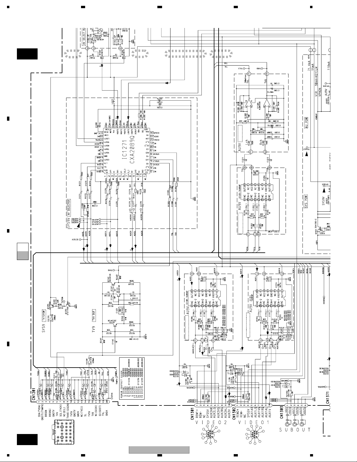
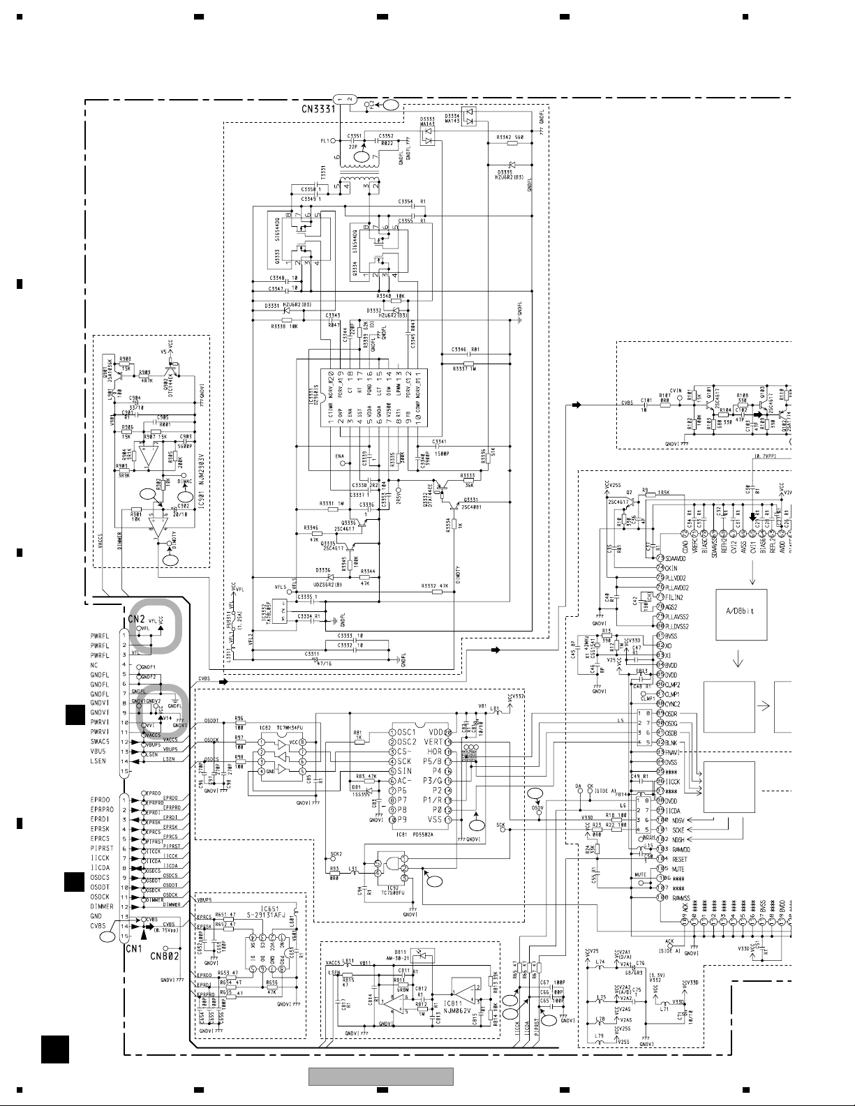
3.2 OVERALL CONNECTION DIAGRAM
A
OPTION TV TUNER
GEX-6100TV/UC
GEX-6100TVP/EW
B
A
MOTHER PCB
B
IR PCB
C
C
RCA PCB
VIDEO3
D
12
1234
AVR-W6100/UC
VIDEO3
& HP OUTPUT
Page 13
A
B
5678
D
CB
SUB OUT
POWER
SUPPLY
MONITOR
PCB
LCD
MODULE
BACK
LIGHT
C
VIDEO2
VIDEO1
AVR-W6100/UC
56
D
7
13
8
Page 14
A-a
A-b
A-b
A-a
1234
3.3 MOTHER PCB(GUIDE PAGE)
Note: When ordering service parts, be sure to refer to " EXPLODED VIEWS AND PARTS LIST" or
"ELECTRICAL PARTS LIST".
VIDEO2 ISOLATOR
VIDEO1 ISOLATOR
A-a
>
TV AUDIO
ISOLATOR
TV AUDIO
AMP
Large size
A-b
A-b
SCH diagram
Guide page
Detailed page
17 18 19 20
13 14 15 16
7 8 9 10 11 12
123456
9
10
6
7
3
9
10
6
7
3
>
>
8
5
4
1
2
8
5
4
1
2
>
>
>
A
A-a A-b
A-a
A-a
B
>
C
CN1581
>
VIDEO3 ISOLATOR
C
>
>
>
CEK1001 4A
1K
IL1801
CEL1735
12V, 5W
IL1802
CEL1735
B
CN1591
BU
SENSE
D
A
14
AVR-W6100/UC
1234
Page 15
A
B
5678
A-b
B
CN1411
2L
1L
2R
1R
: Video Signal
: Audio Signal
MOTHER UNIT
Consists of
MOTHER PCB
IR PCB
RCA PCB
MOTHER PCB
A
HEADPHONE AMP
D
CN2
IICDA
IICCK
D
VAU9
NC
NC
IICRST
MUTEX
SYSTEM CONTROLLER
CRSW
MUTE2
>
>
PWRVI
PWRFL
MUTE1
1-1
1-2
CN1
C
NOTE :
Symbol indicates a resistor.
No differentiation is made between chip resistors and
discrete resistors.
Symbol indicates a capacitor.
No differentiation is made between chip capacitors and
discrete capacitors.
Decimal points for resistor
and capacitor fixed values
are expressed as :
←
2.2 2R2
←
0.022 R022
AVR-W6100/UC
56
The > mark found on some component parts indicates
the importance of the safety factor of the part.
Therefore, when replacing, be sure to use parts of
identical designation.
7
D
A
15
8
Page 16
1234
VAU9
A
B
A-b
1
2
3
4
TV AUDIO
AMP
TV AUDIO
ISOLATOR
A-b
A-a
A-a
C
>
VIDEO2 ISOLATOR
>
>
>
>
VIDEO1 ISOLATOR
>
>
D
A-a
16
17 18 19 20
13 14 15 16
7 8 9 10 11 12
123456
5
4
1
8
2
9
10
3
6
7
5
4
1
8
2
9
10
3
6
7
AVR-W6100/UC
1234
Page 17
A
B
VAU9
5678
PWRVI
PWRFL
5
>
>
6
7
A-b
>
C
VIDEO3 ISOLATOR
CN1581
12V, 5W
IL1802
CEL1735
IL1801
CEL1735
B
CN1591
>
CEK1001 4A
SENSE
A-b
A-a
A-a
C
BU
D
1K
AVR-W6100/UC
56
A-a
7
17
8
Page 18
N
1234
C
CN2
D
1R
2R
1L
A
B
CN1411
2L
HEADPHONE AMP
D
MOTHER PCB
A
B
MOTHER UNIT
Consists of
MOTHER PCB
IR PCB
RCA PCB
A-b
A-a
C
: Video Signal
: Audio Signal
IICDA
IICCK
D
A-b
18
VAU9
1
2
3
4
AVR-W6100/UC
1234
Page 19
A
B
D
CN1
5678
1-2
1-1
The > mark found on some component parts indicates
the importance of the safety factor of the part.
Therefore, when replacing, be sure to use parts of
identical designation.
A-b
MUTE1
MUTE2
CRSW
Decimal points for resistor
IICRST
MUTEX
NC
NC
SYSTEM CONTROLLER
←
←
and capacitor fixed values
are expressed as :
2.2 2R2
0.022 R022
A-a
C
VAU9
PWRVI
PWRFL
5
6
AVR-W6100/UC
56
Symbol indicates a resistor.
No differentiation is made between chip resistors and
discrete resistors.
Symbol indicates a capacitor.
No differentiation is made between chip capacitors and
discrete capacitors.
NOTE :
D
7
A-b
19
7
8
Page 20
1234
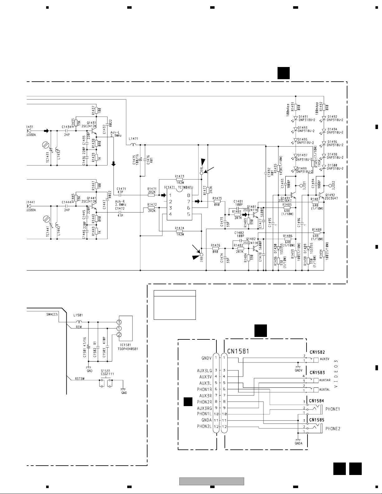
3.4 IR PCB,RCA PCB
10.5V
9.3V
A
B
5V
CN1501
.
C
.
A
CN1802
D
LAMP SWITCH
B
20
1234
AVR-W6100/UC
Page 21
A
B
5678
2-2
2-1
B
IR PCB
MOTHER UNIT
Consists of
MOTHER PCB
REMOTE CONTROL SENSOR
RESET
IR PCB
RCA PCB
CN1371
A
AVR-W6100/UC
56
C
7
C
RCA PCB
D
B C
21
8
Page 22
1234
T
3.5 MONITOR UNIT
A
DIMMER
INVERTER
LCD MODULE
10-1
10-2
FILTER and SYNC AMP
B
2-2
2-1
2-3
>
C
CN1222
5→3V CONVERT
OSD
Y/C SEP.
N
A
OSD
7-3
Interface
7-2
CN1221
A
3-1
D
EEP-ROM
7-4
LIGHT SENSE
9-3
9-4
9-2
D
22
1234
AVR-W6100/UC
Page 23
A
B
5678
MONITOR UNIT
D
YNC AMP
3-2
>
9-1
3.3V
1-1
2.5V
2 SCREEN IC
POWER SUPPLY
1-2
5V
1-3
1-4
RGB AMP
18.5V
8V
-12V
3-3
3-4
5-3
/C SEP.
SD
nterface
NTSC Dec
P in P
Video
Processor
TFT
Controller
VCOM AMP
6-2
5-2
8-3
C
LCD MODULE
5-4
D
: The power supply is shown with the marked box.
AVR-W6100/UC
56
D
7
23
8
Page 24

1234
Note: The encircled numbers denote measuring points in the circuit diagram.
- Mother PCB - IR PCB
CH1 : 1- 1 CVBS
CH2 : 1- 2 REOUT
A
CH1 : 2- 1 IRL
CH2 : 2- 2 IRR
B
C
D
24
1234
AVR-W6100/UC
Page 25

A
B
5678
- Monitor Unit
Note: The encircled numbers denote measuring points in the circuit diagram.
CH1 : 1-1 IC851 Pin3 CH1 : 1-2 IC861 Pin15
CH3 : 1-3 IC861 Pin12
CH1 : 2-1 DIMAC CH3 : 2-3 DIMDTY
CH2 : 2-2 IC901 Pin 6
CH1 : Input (10 step VTRIN) CH3 : 3-2 CVBS2
CH2 : 3-1 CVBS
CH2 : 1-4 IC861 Pin10
CH1 : Input (10 step VTRIN) CH3 : 3-3 GOUT
CH2 : 3-1 CVBS
56
CH4 : 3-4 VG
CH1 : 9-1 V33 CH3 : 9-3 PIPCK
CH2 : 9-2 PIPRST
AVR-W6100/UC
C
CH4 : 9-4 PIPDA
D
25
7
8
Page 26

1234
CH1 : 9-1 V33 CH3 : 9-3 PIPCK
CH2 : 9-2 PIPRST
A
B
CH1 : Input (10 step VTRIN) CH3 : 7-3 OSDV
CH2 : 7-4 POL
CH4 : 9-4 PIPDA
CH4 : 7-2 P0
CH1 : Input (10 step VTRIN) CH3 : 7-3 OSDV
CH2 : 7-4 POL
CH4 : 7-2 P0
CH1 : Input (10 step VTRIN) CH3 : 8-3 VCOM
CH2 : 7-4 POL
CH4 : 3-4 VG
C
CH1 : Input (10 step VTRIN) CH3 : 5-3 STH1
CH2 : 5-2 CX
D
26
1234
CH4 : 3-4 VG
AVR-W6100/UC
CH1 : Input (10 step VTRIN) CH3 : 5-4 STV1
CH2 : 5-2 CX
CH4 : 3-4 VG
Page 27

A
B
5678
CH1 : Input (10 step VTRIN) CH3 : 3-4 VG
CH2 : 6-2 CPH
CH1 : 10-2 FL2
CH1 : 10-1 D3333 Cathode
AVR-W6100/UC
56
C
D
27
7
8
Page 28

1234
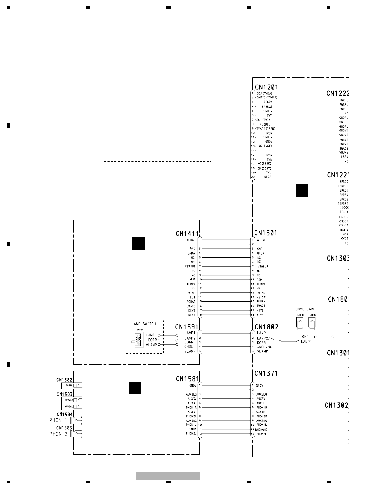
4. PCB CONNECTION DIAGRAM
4.1 MOTHER PCB
NOTE FOR PCB DIAGRAMS
1.The parts mounted on this PCB
include all necessary parts for
A
several destination.
For further information for
respective destinations, be sure
to check with the schematic dia gram.
2.Viewpoint of PCB diagrams
Connector
Capacitor
SIDE A
P.C.Board
A
B
C
Chip Part
MOTHER PCB
SIDE B
D
CN2
C
CN1581
VIDEO2
SIDE A
VIDEO1
SUB OUT
CORD
CN1
D
POWER
SUPPLY
CORD
D
B
CN1411
B
CN1591
A
28
1234
AVR-W6100/UC
Page 29

A
B
MOTHER PCB
A
5678
SIDE B
REM40
AUX3VO
EPRTST
CVBS
C
TP1823
AVR-W6100/UC
56
TP1827
7
D
A
29
8
Page 30

1234
4.2 IR PCB
IR PCB
B
A
B
ADJ
RESET
SIDE A
SOURCE
LAMP
C
TC1431
TC1441
D
B
30
1234
AVR-W6100/UC
Page 31

A
B
5678
B
IR PCB
VIR
A
A
SIDE B
CN1501
CN1802
IRL
IRR
AVR-W6100/UC
56
C
D
B
7
31
8
Page 32

1234
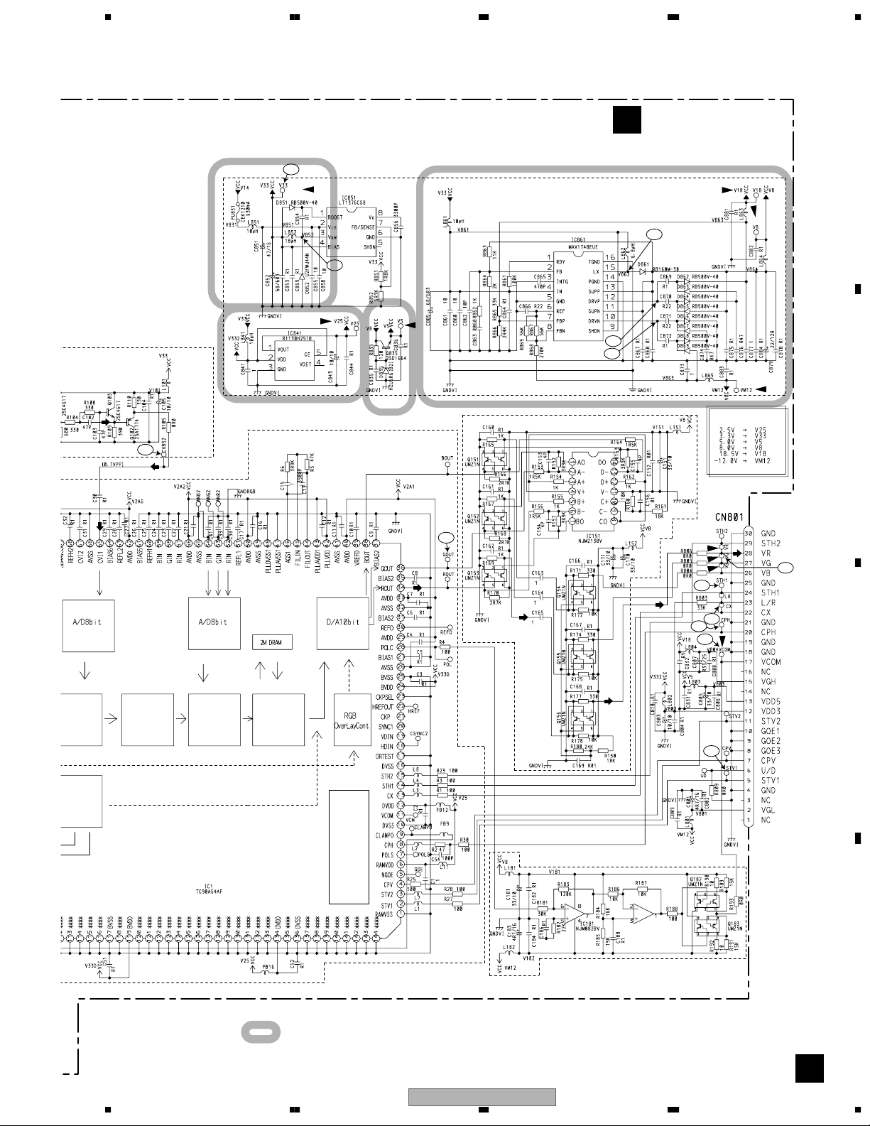
4.3 MONITOR UNIT
MONITOR UNIT
D
A
LCD MODULE
B
SIDE A
A
CN1221
A
C
LCD MODULE
D
CN1222
D
32
AVR-W6100/UC
1234
Page 33

A
B
5678
MONITOR UNIT
D
V33
V25
V8
SIDE B
VM12
V18
V5
VB
VG
VR
VCOM
AVR-W6100/UC
56
C
D
D
7
33
8
Page 34

1234
4.4 RCA PCB
RCA PCB
C
A
PHONE1
B
R
L
SIDE A
C
RCA PCB
SIDE B
1
4
3
6
5
8
7
10
C
D
12
9
11
V
A
PHONE2
CN1371
C
34
AVR-W6100/UC
1234
Page 35

A
B
5678
5. ELECTRICAL PARTS LIST
NOTE:
• Parts whose parts numbers are omitted are subject to being not supplied.
• The part numbers shown below indicate chip components.
Chip Resistor
RS1/_S___J,RS1/__S___J
Chip Capacitor (except for CQS.....)
CKS....., CCS....., CSZS.....
Circuit Symbol and No. Part Name Part No.
D
Unit Number:CWM8246
Unit Name:Monitor Unit
MISCELLANEOUS
IC 1 IC TC90A64AF
IC 81 IC PD5582A
IC 82 IC TC7WH34FU
IC 92 IC TC7S08FU
IC 151 IC NJM2138V
IC 181 IC NJM082BV
IC 651 IC S-29131AFJ
IC 811 IC NJM062V
IC 841 IC R1130H251B
IC 851 IC LT1376CS8
IC 861 IC MAX1748EUE
IC 901 IC NJM2903V
IC 3331 IC OZ960IS
IC 3332 IC TA78L05F
Q 2 Transistor 2SC4617
Q 101 Transistor 2SC4617
Q 102 Transistor 2SA1774
Q 103 Transistor 2SC4617
Q 151 Transistor UMZ1N
Q 152 Transistor UMZ1N
Q 153 Transistor UMZ1N
Q 154 Transistor UMZ1N
Q 155 Transistor UMZ1N
Q 156 Transistor UMZ1N
Q 182 Transistor UMZ1N
Q 183 Transistor UMZ1N
Q 835 Transistor 2SD1664
Q 901 Transistor 2SA1036K
Q 902 Transistor DTC144EK
Q 3331 Transistor 2SC4081
Q 3332 Transistor DTA144EE
Q 3333 FET SI6544DQ
Q 3334 FET SI6544DQ
Q 3335 Transistor 2SC4617
Q 3336 Transistor 2SC4617
D 81 Diode 1SS355
D 811 AM-30-21
D 835 Diode HZU5R6(B2)
D 851 Diode RB500V-40
D 852 Diode U2FWJ44N
D 861 Diode RB160M-30
D 862 Diode RB500V-40
D 863 Diode RB500V-40
D 864 Diode RB500V-40
D 865 Diode RB500V-40
56
D 866 Diode RB500V-40
D 867 Diode RB500V-40
D 868 Diode RB500V-40
D 869 Diode RB500V-40
D 3331 Diode HZU6R2(B3)
D 3332 Diode HZU6R2(B3)
D 3333 Diode MA143
D 3334 Diode MA143
D 3335 Diode HZU6R2(B3)
D 3336 Diode UDZS6R2(B)
L 1 Inductor CTF1306
L 2 Inductor CTF1306
L 3 Inductor CTF1306
L 4 Inductor CTF1306
L 5 Inductor-Array CTF1421
L 6 Inductor-Array CTF1421
L 7 Inductor CTF1306
L 8 Inductor CTF1306
L 11 Inductor CTF1306
L 15 Inductor CTF1306
L 71 Inductor LCKA100J2520
L 74 Inductor LCKA100J2520
L 75 Inductor LCKB100K2520
L 78 Inductor LCKA100J2520
L 79 Inductor CTF1306
L 81 Inductor LCKA101J2520
L 91 Inductor CTF1306
L 101 Inductor LCKB100K2520
L 151 Inductor LCKA100J2520
L 152 Inductor LCKB100K2520
L 181 Inductor LCKA101J2520
L 182 Inductor LCKA101J2520
L 601 Inductor LCKA100J2520
L 801 Inductor LCKA100J2520
L 802 Inductor LCKA100J2520
L 803 Inductor LCKA100J2520
L 804 Inductor LCKA100J2520
L 811 Inductor LCTB100K1608
L 841 Choke Coil 10µH CTH1249
L 851 Choke Coil 10µH CTH1259
L 852 Choke Coil 18µH CTH1250
L 861 Choke Coil 10µH CTH1249
L 862 Choke Coil 6.8µH CTH1248
L 863 Inductor LCTB100K1608
L 864 Inductor LCKB100K2520
L 865 Inductor LCKA100J2520
L 901 Inductor LCKB100K2520
L 3311 Inductor CTH1256
T 3331 T r ansf ormer CTT1103
X 1 Crystal Resonator 42MHz CSS1541
FU831 Fuse 630mA CEK1210
FU3311 Fuse 1.25A CEK1205
AVR-W6100/UC
Circuit Symbol and No. Part Name Part No.
7
C
D
35
8
Page 36

1234
Circuit Symbol and No. Part Name Part No.
FB13 Ferrite Beed CTF1528
FB16 Ferrite Beed CTF1528
FB12 Ferrite Beed CTF1528
FB14 Ferrite Beed CTF1528
FB9 Ferrite Beed CTF1528
A
RESISTORS
R 1 RS1/16S101J
R 2 RS1/16S470J
R 3 RS1/16S101J
R 4 RS1/16S101J
R 5 RS1/16S473J
R 6 RS1/16S392J
R 9 RS1/16S152J
R 10 RS1/16S331J
R 12 RS1/16SS105J
R 13 RS1/16S391J
R 18 RS1/16S101J
R 22 RS1/16S101J
R 23 RS1/16S0R0J
R 24 RS1/16S333J
R 25 RS1/16S101J
R 27 RS1/16S101J
B
R 28 RS1/16S101J
R 29 RS1/16S101J
R 30 RS1/16S101J
R 65 RS1/16S470J
R 66 RS1/16S470J
R 67 RS1/16S470J
R 81 RS1/16S102J
R 83 RS1/16S473J
R 93 RS1/16S0R0J
R 96 RS1/16S101J
R 97 RS1/16S101J
R 98 RS1/16S101J
R 101 RS1/16S1502F
R 102 RS1/16S1003F
R 103 RS1/16S681J
R 104 RS1/16S331J
R 105 RS1/16S0R0J
R 107 RS1/16S0R0J
C
R 108 RS1/16S331J
R 109 RS1/16S391J
R 110 RS1/16S391J
R 150 RS1/16S183J
R 152 RS1/16S3901F
R 153 RS1/16S1501F
R 154 RS1/16S102J
R 155 RS1/16S102J
R 156 RS1/16S1501F
R 157 RS1/16S3901F
R 160 RS1/16S1002F
R 161 RS1/16S1802F
R 162 RS1/16S102J
R 163 RS1/16S3901F
R 164 RS1/16S1501F
R 165 RS1/16S102J
R 166 RS1/16S272J
D
R 167 RS1/16S102J
R 168 RS1/16S272J
R 169 RS1/16S102J
R 170 RS1/16S272J
R 171 RS1/16S331J
R 172 RS1/16S103J
Circuit Symbol and No. Part Name Part No.
R 174 RS1/16S331J
R 175 RS1/16S103J
R 177 RS1/16S331J
R 178 RS1/16S103J
R 180 RS1/16S243J
R 181 RS1/16S3002F
R 182 RS1/16S223J
R 183 RS1/16S1203F
R 184 RS1/16S1602F
R 185 RS1/16S1502F
R 186 RS1/16S1002F
R 187 RS1/16S1002F
R 188 RS1/16S101J
R 189 RS1/16S153J
R 190 RS1/16S100J
R 191 RS1/16S153J
R 192 RS1/16S100J
R 193 RS1/16S0R0J
R 651 RS1/16S470J
R 652 RS1/16S470J
R 653 RS1/16S470J
R 654 RS1/16S470J
R 655 RS1/16S470J
R 656 RS1/16S473J
R 803 RS1/16S333J
R 804 RS1/16S0R0J
R 805 RS1/16S0R0J
R 806 RS1/16S0R0J
R 809 RS1/16S0R0J
R 811 RS1/16S685J
R 812 RS1/16S105J
R 813 RS1/16S393J
R 814 RS1/16S103J
R 815 RS1/16S470J
R 835 RS1/16S121J
R 851 RS1/16S182J
R 852 RS1/16S512J
R 861 RS1/16S104J
R 862 RS1/16S102J
R 863 RS1/16S1102F
R 864 RS1/16S2001F
R 865 RS1/16S3302F
R 866 RS1/16S2401F
R 867 RS1/16S5602F
R 868 RS1/16S2703F
R 869 RS1/16S5602F
R 901 RS1/16S103J
R 902 RS1/16S103J
R 903 RS1/16S392J
R 904 RS1/16S912J
R 905 RS1/16S2003F
R 906 RS1/16S153J
R 907 RS1/16S153J
R 908 RS1/16S153J
R 909 RS1/16S472J
R 3331 RS1/16S105J
R 3332 RS1/16S473J
R 3333 RS1/16S363J
R 3334 RS1/16S102J
R 3335 RS1/16S304J
R 3336 RS1/16S513J
R 3337 RS1/16S105J
R 3338 RS1/16S103J
R 3339 RN1/16SC6202D
36
AVR-W6100/UC
1234
Page 37

A
B
5678
Circuit Symbol and No. Part Name Part No.
R 3340 RS1/16S103J
R 3342 RS1/16S561J
R 3344 RS1/16S473J
R 3345 RS1/16S104J
R 3346 RS1/16S473J
CAPACITORS
C 1 CKSRYB105K10
C 2 CKSSYF104Z16
C 3 CKSSYF104Z16
C 4 CKSSYF104Z16
C 5 CKSSYF104Z16
C 6 CKSSYF104Z16
C 7 CKSSYF104Z16
C 8 CKSSYF104Z16
C 9 CKSSYF104Z16
C 10 CKSSYF104Z16
C 11 CKSSYF104Z16
C 12 CKSSYF104Z16
C 13 CKSRYB392K50
C 15 CKSRYB105K10
C 16 CKSSYF104Z16
C 17 CKSSYF104Z16
C 21 CKSSYF104Z16
C 22 CKSSYF104Z16
C 23 CKSSYF104Z16
C 24 CKSSYF104Z16
C 25 CKSSYF104Z16
C 26 CKSSYF104Z16
C 27 CKSSYF104Z16
C 28 CKSSYF104Z16
C 29 CKSSYF104Z16
C 30 CKSRYB104K16
C 31 CKSSYF104Z16
C 32 CKSSYF104Z16
C 33 CKSSYF104Z16
C 34 CKSSYF104Z16
C 35 CKSRYB103K25
C 36 CCSRCH4R0C50
C 37 CKSSYF104Z16
C 38 CKSSYF104Z16
C 39 CKSSYF104Z16
C 40 CKSSYF104Z16
C 41 CKSSYF104Z16
C 42 CCSRCH181J50
C 45 CCSRCH8R0D50
C 46 CCSRCH8R0D50
C 47 CKSSYF104Z16
C 48 CKSSYF104Z16
C 49 CKSSYF104Z16
C 50 CKSRYB105K10
C 51 CKSSYF104Z16
C 52 CKSSYF104Z16
C 54 CCSRCH101J50
C 55 CKSRYF104Z25
C 65 CCSRCH101J50
C 66 CCSRCH101J50
C 67 CCSRCH101J50
C 71 CSZS100M10
C 75 CKSRYB105K10
C 76 68µF/6.3V CCH1440
C 81 CSZS100M10
C 82 CKSRYF104Z25
C 83 CKSRYB105K10
Circuit Symbol and No. Part Name Part No.
C 85 CKSRYF104Z25
C 94 CKSRYF104Z25
C 96 CCSRCH271J50
C 97 CCSRCH271J50
C 98 CCSRCH271J50
C 101 CKSYF106Z10
C 102 CCSRCH470J50
C 103 CCSRCH470J50
C 104 CKSRYF104Z25
C 105 CSZS100M10
C 151 CSZSR330M10
C 152 CKSRYB103K25
C 153 CCSRCH4R0C50
C 154 CCSRCH4R0C50
C 155 CCSRCH4R0C50
C 156 CKSRYF104Z25
C 160 CKSRYF104Z25
C 161 CKSRYF104Z25
C 162 CKSRYF104Z25
C 163 CKSRYB105K10
C 164 CKSRYB105K10
C 165 CKSRYB105K10
C 166 CKSRYF104Z25
C 167 CKSRYF104Z25
C 168 CKSRYF104Z25
C 169 CKSRYB103K25
C 170 CSZSR330M10
C 171 CSZSR330M10
C 181 CSZSR330M10
C 182 CKSRYF104Z25
C 183 CSZSR4R7M16
C 184 CKSRYF104Z25
C 186 CKSRYF104Z25
C 188 CKSRYF104Z25
C 651 CKSRYF104Z25
C 652 CCSRCH101J50
C 653 CCSRCH101J50
C 654 CCSRCH101J50
C 655 CCSRCH101J50
C 656 CCSRCH101J50
C 801 CSZSR4R7M16
C 802 CKSRYF104Z25
C 803 CSZS100M10
C 804 CKSRYF104Z25
C 805 CSZSR330M10
C 806 CKSRYF104Z25
C 807 CSZSR33M25
C 808 CKSRYF104Z25
C 809 CKSSYF104Z16
C 810 CKSSYF104Z16
C 811 CKSRYB104K16
C 812 CKSRYF104Z25
C 813 CKSRYF104Z25
C 814 CKSRYF104Z25
C 815 CKSRYF104Z25
C 817 CKSRYF104Z25
C 831 CKSSYF104Z16
C 832 CKSRYF104Z25
C 835 CKSRYB104K16
C 836 CKSRYB104K16
C 841 CKSRYB105K10
C 843 CSZS100M10
C 844 CKSRYF104Z25
C 851 47µF/16V CCH1446
C
D
AVR-W6100/UC
56
7
8
37
Page 38

1234
Circuit Symbol and No. Part Name Part No.
C 852 68µF/6.3V CCH1440
C 853 CKSRYB104K16
C 854 CKSRYB104K16
C 855 10µF CCG1170
C 856 CKSRYB332K50
C 858 10µF CCG1170
A
C 859 CKSRYB104K16
C 860 CKSYB106K6R3
C 861 CKSYB106K6R3
C 862 CCSRCH100D50
C 863 CKSRYB683K16
C 864 CKSRYB104K16
C 865 CKSRYB471K50
C 866 CKSRYB224K16
C 867 CKSRYB104K16
C 868 CKSRYB104K16
C 869 CKSRYB104K16
C 870 CKSRYB224K16
C 871 CKSRYB224K16
C 872 CKSRYB104K16
C 873 CKSQYB105K16
C 874 CKSQYB474K25
C 875 CKSRYB104K16
C 876 CKSQYB474K25
B
C 877 CKSQYB105K16
C 878 CKSRYB104K16
C 879 22µF/12V CCH1359
C 881 CKSRYF104Z25
C 882 CKSRYF104Z25
C 883 CKSRYF104Z25
C 884 CKSRYB104K16
C 885 68µF/6.3V CCH1440
C 901 CKSRYF104Z25
C 902 CSZSR220M10
C 903 CFHSQ562J16
C 904 CSZSR330M10
C 905 CCSRCH102J50
C 3311 47µF/16V CCH1446
C 3332 10µF CCG1170
C 3333 10µF CCG1170
C 3334 CKSRYF104Z25
C
C 3335 CKSQYB105K16
C 3336 CKSRYB105K10
C 3337 CKSQYB105K16
C 3338 CKSQYB225K10
C 3339 CKSQYB105K16
C 3340 CKSRYB392K50
C 3341 CKSRYB152K50
C 3343 CKSRYB473K25
C 3344 CCSRCH221J50
C 3345 CKSRYB473K25
C 3346 CKSRYB103K25
C 3347 10µF CCG1170
C 3348 10µF CCG1170
C 3349 CKSQYB105K16
C 3350 CKSQYB105K16
C 3351 22pF CCG1140
C 3352 CKSRYB223K50
C 3353 CKSRYF104Z25
D
C 3354 CKSRYB104K16
C 3355 CKSRYB104K16
Circuit Symbol and No. Part Name Part No.
ABC
Mother Unit
Consists of
Mother PCB
IR PCB
RCA PCB
Unit Number:
CWM8247 (AVR-W6100/UC)
:CWM8250 (AVR-W6100/EW)
Unit Name:Mother Unit
MISCELLANEOUS
IC 1201 IC NJM4558E
IC 1221 IC NJM2267M
IC 1251 IC TA2050F
IC 1271 IC CXA2089Q
IC 1301 IC TA2050F
IC 1311 IC TA2050F
IC 1321 IC TA2050F
IC 1371 IC TDA7496L
IC 1411 IC BA3308FV
IC 1471 IC TC7W04FU
IC 1501 IC TSOP4840SB1
IC 1521 IC NJM555V
IC 1522 IC TC7S66FU
IC 1531 IC TC7W02FU
IC 1601 IC PE5304B
IC 1801 IC TA78L05F
IC 1861 IC PAJ001A
Q 1111 Transistor 2SC2412K
Q 1112 Transistor 2SC2412K
Q 1113 Transistor FMG12
Q 1131 Transistor 2SC2412K
Q 1132 Transistor 2SC2412K
Q 1133 Transistor FMG12
Q 1141 Transistor 2SC2412K
Q 1142 Transistor 2SC2412K
Q 1151 Transistor 2SC2412K
Q 1261 Transistor 2SC2412K
Q 1262 Transistor 2SC2412K
Q 1263 Transistor 2SA1037K
Q 1264 Transistor 2SA1037K
Q 1291 Transistor 2SA1036K
Q 1292 Transistor DTC114EK
Q 1351 Transistor 2SA1037K
Q 1352 Transistor 2SC2412K
Q 1401 Transistor 2SD1664
Q 1431 Transistor 2SC2412K
Q 1441 Transistor 2SC2412K
Q 1451 Transistor 2SC3518-Z
Q 1461 Transistor 2SD1664
Q 1481 Transistor 2SC2411K
Q 1482 Transistor 2SC2411K
Q 1491 Transistor 2SC3647
Q 1492 Transistor 2SC3647
Q 1621 Transistor DTA144EK
Q 1622 Transistor DTA144EK
Q 1801 Transistor 2SA1036K
Q 1802 Transistor 2SC2412K
Q 1811 Transistor 2SA1036K
Q 1812 Transistor DTC114EK
Q 1813 Transistor 2SD2375
38
AVR-W6100/UC
1234
Page 39

A
B
5678
Circuit Symbol and No. Part Name Part No.
Q 1821 Transistor 2SA1385-Z
Q 1822 Transistor DTC114EK
Q 1823 Transistor 2SD1760F5
Q 1827 Transistor 2SD1664
Q 1835 Transistor 2SC3518-Z
Q 1841 Transistor 2SA1615-Z
Q 1842 Transistor DTC114EK
Q 1843 Transistor 2SB1260
Q 1844 Transistor DTC114EK
Q 1862 Transistor DTC114EK
Q 1891 Transistor 2SC3518-Z
Q 1892 Transistor 2SA1036K
Q 1893 Transistor DTC114EK
D 1111 Diode MA152WA
D 1131 Diode MA152WA
D 1201 Diode HZU5R6(B2)
D 1203 Diode HZU5R6(B2)
D 1204 Diode HZU5R6(B2)
D 1206 Diode HZU2R0(B)
D 1207 Diode HZU5R6(B2)
D 1209 Diode HZU5R6(B2)
D 1213 Diode HZU5R6(B2)
D 1214 Diode HZU5R6(B2)
D 1216 Diode HZU5R6(B2)
D 1218 Diode HZU5R6(B2)
D 1219 Diode HZU5R6(B2)
D 1226 Diode HZU2R0(B)
D 1231 Diode MA153
D 1236 Diode HZU5R6(B2)
D 1239 Diode HZU5R6(B2)
D 1271 Diode HZU2R0(B)
D 1272 Diode HZU2R0(B)
D 1275 Diode HZU2R0(B)
D 1276 Diode HZU2R0(B)
D 1301 Diode HZU5R6(B2)
D 1302 Diode HZU5R6(B2)
D 1303 Diode HZU5R6(B2)
D 1304 Diode HZU5R6(B2)
D 1311 Diode HZU5R6(B2)
D 1312 Diode HZU5R6(B2)
D 1313 Diode HZU5R6(B2)
D 1314 Diode HZU5R6(B2)
D 1321 Diode HZU5R6(B2)
D 1322 Diode HZU5R6(B2)
D 1323 Diode HZU5R6(B2)
D 1324 Diode HZU5R6(B2)
D 1331 Diode HZU2R0(B)
D 1332 Diode HZU2R0(B)
D 1333 Diode HZU2R0(B)
D 1334 Diode HZU2R0(B)
D 1352 Diode MA153
D 1353 Diode 1SS355
D 1401 Diode HZU5R6(B2)
D 1431 Diode HVU200A
D 1441 Diode HVU200A
D 1451 Diode HZU11(B2)
D 1461 Diode UDZ10(B)
D 1489 Diode 1SS355
D 1490 Diode 1SS355
D 1491 LED DNP318U-2
D 1492 LED DNP318U-2
D 1493 LED DNP318U-2
D 1494 LED DNP318U-2
D 1495 LED DNP318U-2
Circuit Symbol and No. Part Name Part No.
D 1496 LED DNP318U-2
D 1497 LED DNP318U-2
D 1498 LED DNP318U-2
D 1499 LED DNP318U-2
D 1500 LED DNP318U-2
D 1551 Diode HZU5R6(B2)
D 1553 Diode HZU5R6(B2)
D 1561 LED CL191G1C
D 1562 LED CL191G1C
D 1563 Chip LED CL190SDCD
D 1564 LED CL191G1C
D 1565 Chip LED CL190SDCD
D 1569 LED CL191G1C
D 1801 Diode SC016-2
D 1811 Diode UDZ10(B)
D 1823 Diode UDZ10(B)
D 1827 Diode HZU5R6(B2)
D 1835 Diode UDZ10(B)
D 1861 Diode SC016-2
D 1862 Diode UDZS18(B)
D 1891 Diode PTZ18A
L 1221 Inductor LCKA150J2520
L 1271 Inductor LCKA100J2520
L 1371 Inductor CTH1256
L 1431 Inductor LCYC100K2125
L 1432 Inductor LCKA680J2520
L 1441 Inductor LCYC100K2125
L 1442 Inductor LCKA470J2520
L 1471 Inductor LCKB100K2520
L 1491 Inductor LCKB6R8M2520
L 1501 Inductor LCKA101J2520
L 1521 Inductor LCKA100J2520
L 1601 Inductor CTF1306
L 1602 Inductor CTF1306
L 1661 Inductor LCKA150J2520
L 1662 Inductor LCKA150J2520
L 1663 Inductor LCKA150J2520
L 1664 Inductor LCKA2R2J2520
L 1801 Choke Coil 2.4mH CTH1101
L 1819 Choke Coil 2.2mH CTH1277
L 1841 Choke Coil 100µH CTH1140
L 1842 Inductor CTH1256
TC1431 Trimmer CCL1057
TC1441 Trimmer CCL1057
X 1601 Radiator 12.58MHz CSS1601
S 1531 Push Switch CSG1111
S 1561 Push Switch CSG1111
S 1562 Push Switch CSG1111
S 1564 Push Switch CSG1111
S 1565 Push Switch CSG1111
S 1566 Push Switch CSG1111
S 1567 Push Switch CSG1111
S 1568 Push Switch CSG1111
S 1591 Switch(LAMP) CSH1061
S 1601 Push Switch(DEG0) CSG1153
VR1261 Semi-fixed 4.7kΩ(B) CCP1446
VR1361 Semi-fixed 3.3kΩ(B) CCP1445
FU1201 Fuse 630mA CEK1210
FU1291 Fuse 200mA CEK1189
FU1301 Fuse 2A CEK1190
FU1302 Fuse 200mA CEK1189
FU1311 Fuse 2A CEK1190
FU1312 Fuse 200mA CEK1189
FU1331 Fuse 2A CEK1190
C
D
AVR-W6100/UC
56
7
8
39
Page 40

1234
Circuit Symbol and No. Part Name Part No.
FU1332 Fuse 2A CEK1190
FU1841 Fuse 630mA CEK1210
FU1842 Fuse 2A CEK1190
EF1621 Filter CCG1067
EF1622 Filter CCG1067
EF1671 Filter CCG1067
A
EF1672 Filter CCG1067
EF1679 Filter CCG1067
BZ1601 Buzzer CPV1050
RESISTORS
R 1101 RS1/16S182J
R 1102 RS1/16S182J
R 1111 RS1/16S471J
R 1112 RS1/16S471J
R 1113 RS1/16S821J
R 1114 RS1/16S821J
R 1115 RS1/16S104J
R 1116 RS1/16S104J
R 1117 RS1/16S821J
R 1118 RS1/16S821J
R 1121 RS1/16S182J
R 1122 RS1/16S182J
B
R 1131 RS1/16S471J
R 1132 RS1/16S471J
R 1133 RS1/16S821J
R 1134 RS1/16S821J
R 1135 RS1/16S104J
R 1136 RS1/16S104J
R 1137 RS1/16S821J
R 1138 RS1/16S821J
R 1141 RS1/10S0R0J
R 1142 RS1/16S223J
R 1143 RS1/16S223J
R 1145 RS1/16S102J
R 1146 RS1/16S102J
R 1147 RS1/16S220J
R 1148 RS1/16S332J
R 1149 RS1/16S0R0J
R 1151 RS1/16S223J
R 1152 RS1/16S223J
C
R 1153 RS1/16S222J
R 1154 RS1/16S471J
R 1155 RS1/16S471J
R 1201 RS1/16S182J
R 1202 RS1/16S182J
R 1203 RS1/16S103J
R 1204 RS1/16S103J
R 1205 RS1/16S822J
R 1206 RS1/16S822J
R 1207 RS1/16S223J
R 1208 RS1/16S103J
R 1209 RS1/16S103J
R 1210 RS1/16S103J
R 1213 RS1/16S750J
R 1224 RS1/16S0R0J
R 1231 RS1/16S105J
R 1232 RS1/16S750J
D
R 1251 RS1/16S101J
R 1252 RS1/16S101J
R 1253 RS1/16S223J
R 1254 RS1/16S223J
R 1255 RS1/16S102J
R 1256 RS1/16S102J
Circuit Symbol and No. Part Name Part No.
R 1261 RS1/16S123J
R 1262 RS1/16S471J
R 1263 RS1/16S103J
R 1264 RS1/16S471J
R 1265 RS1/16S103J
R 1266 RS1/16S562J
R 1267 RS1/16S102J
R 1268 RS1/16S102J
R 1269 RS1/16S104J
R 1271 RS1/16S562J
R 1272 RS1/16S562J
R 1273 RS1/16S470J
R 1274 RS1/16S562J
R 1275 RS1/16S562J
R 1276 RS1/16S470J
R 1277 RS1/16S562J
R 1278 RS1/16S562J
R 1279 RS1/16S470J
R 1280 RS1/16S562J
R 1281 RS1/16S562J
R 1282 RS1/16S470J
R 1285 RS1/16S101J
R 1286 RS1/16S101J
R 1287 RS1/16S750J
R 1288 RS1/16S750J
R 1289 RS1/16S271J
R 1291 RS1/16S223J
R 1292 RS1/16S332J
R 1301 RS1/16S101J
R 1302 RS1/16S101J
R 1303 RS1/16S223J
R 1304 RS1/16S223J
R 1305 RS1/16S102J
R 1306 RS1/16S102J
R 1311 RS1/16S101J
R 1312 RS1/16S101J
R 1313 RS1/16S223J
R 1314 RS1/16S223J
R 1315 RS1/16S102J
R 1316 RS1/16S102J
R 1321 RS1/16S101J
R 1322 RS1/16S101J
R 1323 RS1/16S223J
R 1324 RS1/16S223J
R 1325 RS1/16S102J
R 1326 RS1/16S102J
R 1333 RS1/16S750J
R 1352 RS1/16S473J
R 1353 RS1/16S473J
R 1354 RS1/16S473J
R 1355 RS1/16S473J
R 1356 RS1/16S472J
R 1371 RS1/16S334J
R 1372 RS1/16S103J
R 1373 RS1/10S101J
R 1374 RS1/10S101J
R 1375 RS1/10S101J
R 1376 RS1/10S101J
R 1377 RS1/16S0R0J
R 1401 RS1/16S821J
R 1411 RS1/16S183J
R 1412 RS1/16S183J
R 1413 RS1/16S561J
R 1414 RS1/16S561J
40
AVR-W6100/UC
1234
Page 41

A
B
5678
Circuit Symbol and No. Part Name Part No.
R 1415 RS1/16S124J
R 1416 RS1/16S124J
R 1417 RS1/16S221J
R 1418 RS1/16S221J
R 1419 RS1/16S222J
R 1420 RS1/16S222J
R 1421 RS1/16S564J
R 1422 RS1/16S184J
R 1423 RS1/16S184J
R 1431 RS1/16S103J
R 1432 RS1/16S104J
R 1433 RS1/16S473J
R 1435 RS1/16S393J
R 1437 RS1/16S101J
R 1438 RS1/16S0R0J
R 1439 RS1/16S102J
R 1441 RS1/16S103J
R 1442 RS1/16S104J
R 1443 RS1/16S473J
R 1445 RS1/16S393J
R 1447 RS1/16S101J
R 1448 RS1/16S0R0J
R 1449 RS1/16S102J
R 1451 RS1/10S681J
R 1461 RS1/10S681J
R 1471 RS1/16S222J
R 1472 RS1/16S222J
R 1473 RS1/16S125J
R 1474 RS1/16S125J
R 1475 RS1/16S0R0J
R 1476 RS1/16S0R0J
R 1477 RS1/16S222J
R 1481 RS1/16S272J
R 1482 RS1/16S272J
R 1483 RS1/16S391J
R 1484 RS1/16S391J
R 1485 RS1/10S6R8J
R 1486 RS1/10S6R8J
R 1487 RS1/10S6R8J
R 1488 RS1/10S6R8J
R 1491 RS1/4S0R0J
R 1492 RS1/4S0R0J
R 1493 RS1/10S101J
R 1494 RS1/10S101J
R 1495 RS1/10S152J
R 1496 RS1/10S331J
R 1497 RS1/10S152J
R 1498 RS1/10S331J
R 1521 RS1/16S473J
R 1522 RN1/16SE1302D
R 1523 RN1/16SE1001D
R 1524 RN1/16SE8201D
R 1525 RN1/16SE4700D
R 1526 RN1/16SE1501D
R 1527 RS1/16S0R0J
R 1531 RS1/10S0R0J
R 1533 RS1/16S101J
R 1534 RS1/16S101J
R 1537 RS1/16S0R0J
R 1551 RS1/10S102J
R 1552 RS1/10S102J
R 1553 RS1/10S102J
R 1554 RS1/10S102J
R 1555 RS1/4S181J
Circuit Symbol and No. Part Name Part No.
R 1556 RS1/10S0R0J
R 1557 RS1/10S0R0J
R 1558 RS1/10S0R0J
R 1562 RS1/16S152J
R 1563 RS1/16S332J
R 1564 RS1/16S103J
R 1566 RS1/16S152J
R 1567 RS1/16S332J
R 1568 RS1/16S103J
R 1601 RS1/16S472J
R 1602 RS1/16S472J
R 1604 RS1/16S681J
R 1605 RS1/16S471J
R 1609 RAB4CQ681J
R 1610 (AVR-W6100/UC) RS1/16S473J
R 1611 (AVR-W6100/EW) RS1/16S473J
R 1612 RS1/16S473J
R 1613 RS1/16S473J
R 1615 RS1/16S681J
R 1621 RS1/16S681J
R 1622 RS1/16S681J
R 1623 RS1/16S681J
R 1624 RAB4CQ681J
R 1628 RS1/16S473J
R 1629 RS1/16S473J
R 1630 RS1/16S473J
R 1631 RS1/16S272J
R 1632 RS1/16S272J
R 1634 RS1/16S681J
R 1635 RS1/16S473J
R 1636 RS1/16S681J
R 1637 RS1/16S681J
R 1638 RS1/16S471J
R 1639 RS1/16S470J
R 1640 RS1/16S470J
R 1641 RAB4CQ681J
R 1642 RS1/16S470J
R 1643 RS1/16S470J
R 1644 RAB4CQ681J
R 1645 RAB4CQ681J
R 1646 RS1/16S103J
R 1647 RS1/16S103J
R 1648 RS1/16S0R0J
R 1649 RS1/16S473J
R 1661 RAB4CQ681J
R 1662 RAB4CQ681J
R 1663 RS1/16S0R0J
R 1664 RS1/16S681J
R 1665 RS1/16S471J
R 1666 RS1/16S0R0J
R 1671 RS1/16S681J
R 1672 RS1/16S681J
R 1676 RS1/16S103J
R 1679 RS1/16S681J
R 1695 RS1/16S473J
R 1801 RS1/16S0R0J
R 1802 RS1/16S562J
R 1803 RS1/16S153J
R 1804 RS1/16S473J
R 1805 RS1/16S473J
R 1811 RS1/16S223J
R 1812 RS1/16S182J
R 1813 RS1/10S102J
R 1816 RS1/10S104J
C
D
AVR-W6100/UC
56
7
8
41
Page 42

1234
Circuit Symbol and No. Part Name Part No.
R 1821 RS1/16S153J
R 1822 RS1/4S301J
R 1823 RS1/4S301J
R 1824 RS1/10S681J
R 1827 RS1/10S681J
R 1829 RS1/4S0R0J
A
R 1830 RS1/4S0R0J
R 1835 RS1/10S681J
R 1841 RS1/16S153J
R 1842 RS1/4S301J
R 1843 RS1/4S301J
R 1844 RS1/16S153J
R 1845 RS1/4S152J
R 1863 RN1/10SE1001D
R 1864 RS1/16S223J
R 1865 RS1/16S103J
R 1866 RS1/16S104J
R 1867 RS1/16S104J
R 1868 RS1/16S104J
R 1870 RS1/16S101J
R 1871 RS1/16S104J
R 1872 RS1/16S563J
R 1873 RS1/16S393J
R 1874 RS1/16S363J
B
R 1875 RS1/16S753J
R 1884 RS1/16S473J
R 1890 RS1/16S473J
R 1891 RS1/4S100J
R 1892 RS1/10S103J
R 1893 RS1/10S103J
R 1894 RS1/4S100J
CAPACITORS
C 1101 CKSRYB222K50
C 1102 CKSRYB222K50
C 1103 CKSRYB104K25
C 1111 CEV100M16
C 1112 CEV100M16
C 1113 CKSRYB222K50
C 1114 CKSRYB222K50
C 1121 CKSRYB222K50
C
C 1122 CKSRYB222K50
C 1123 CKSRYB104K25
C 1131 CEV100M16
C 1132 CEV100M16
C 1133 CKSRYB222K50
C 1134 CKSRYB222K50
C 1141 CKSQYB103K50
C 1142 10µF/16V CCG1138
C 1143 CKSQYB105K16
C 1144 CCSRCH100D50
C 1151 CCSRCH101J50
C 1201 CKSRYB222K50
C 1202 CKSRYB222K50
C 1203 CCSRCH101J50
C 1204 CCSRCH101J50
C 1205 100µF/16V CCH1228
C 1206 CKSRYB104K25
D
C 1207 100µF/16V CCH1228
C 1211 10µF/16V CCG1138
C 1212 10µF/16V CCG1138
C 1221 CKSRYB103K50
C 1225 100µF/16V CCH1228
C 1226 CKSRYB103K50
Circuit Symbol and No. Part Name Part No.
C 1231 CEV4R7M35
C 1235 CEV220M16
C 1236 100µF/16V CCH1228
C 1251 CKSRYB105K10
C 1252 CKSRYB105K10
C 1253 CKSRYB105K10
C 1254 CKSRYB105K10
C 1255 100µF/16V CCH1228
C 1256 10µF/16V CCG1138
C 1257 CCSRCH471J50
C 1261 CCSRCH8R0D50
C 1262 CCSRCH120J50
C 1271 CKSRYB105K10
C 1272 CKSRYB105K10
C 1273 CKSRYB474K10
C 1274 CKSRYB105K10
C 1275 CKSRYB105K10
C 1276 CKSRYB474K10
C 1277 CKSRYB105K10
C 1278 CKSRYB105K10
C 1279 CKSRYB474K10
C 1280 CKSRYB105K10
C 1281 CKSRYB105K10
C 1282 CKSRYB474K10
C 1286 CKSRYB103K50
C 1287 CEV220M16
C 1288 CEV100M16
C 1289 CCSRCH221J50
C 1290 CCSRCH101J50
C 1301 CKSRYB105K10
C 1302 CKSRYB105K10
C 1303 CKSRYB105K10
C 1304 CKSRYB105K10
C 1305 CEV220M16
C 1306 CEV100M16
C 1307 CCSRCH471J50
C 1308 CCSRCH471J50
C 1311 CKSRYB105K10
C 1312 CKSRYB105K10
C 1313 CKSRYB105K10
C 1314 CKSRYB105K10
C 1315 CEV220M16
C 1316 CEV100M16
C 1317 CCSRCH471J50
C 1318 CCSRCH471J50
C 1321 CKSRYB105K10
C 1322 CKSRYB105K10
C 1323 CKSRYB105K10
C 1324 CKSRYB105K10
C 1325 CEV220M16
C 1326 CEV100M16
C 1327 CCSRCH471J50
C 1328 CCSRCH471J50
C 1351 CKSRYB103K50
C 1371 CEHAT102M16
C 1372 CKSQYB104K50
C 1373 CKSQYB474K25
C 1374 CKSQYB474K25
C 1375 CKSQYB104K50
C 1376 CEHAT331M16
C 1377 CKSQYB105K16
C 1378 CEHAT471M25
C 1379 CEHAT471M25
C 1401 CKSRYB105K10
42
AVR-W6100/UC
1234
Page 43

A
B
5678
Circuit Symbol and No. Part Name Part No.
C 1402 CKSRYB103K50
C 1403 100µF/16V CCH1228
C 1405 100µF/16V CCH1228
C 1411 CCSRCH221J50
C 1412 CCSRCH221J50
C 1413 CCSRCH101J50
C 1414 CCSRCH101J50
C 1415 CKSRYB393K16
C 1416 CKSRYB393K16
C 1417 CEV4R7M25
C 1418 CEV4R7M25
C 1421 CEV470M16
C 1422 100µF/16V CCH1228
C 1423 CKSRYB103K50
C 1431 CKSRYB103K50
C 1432 CCSRCH471J50
C 1434 CCSRCH240J50
C 1435 CCSRCH221J50
C 1436 CCSRCH221J50
C 1437 CKSRYB223K50
C 1438 CKSQYB225K10
C 1441 CKSRYB103K50
C 1442 CCSRCH471J50
C 1444 CCSRCH240J50
C 1445 CCSRCH221J50
C 1446 CCSRCH221J50
C 1447 CKSRYB223K50
C 1448 CKSQYB225K10
C 1451 100µF/16V CCH1228
C 1452 CKSRYB103K50
C 1453 CKSRYB103K50
C 1454 100µF/16V CCH1228
C 1461 100µF/16V CCH1228
C 1462 CKSRYB103K50
C 1463 CKSRYB103K50
C 1464 100µF/16V CCH1228
C 1471 CCSRCH470J50
C 1472 CCSRCH470J50
C 1473 CCSRCH330J50
C 1474 CCSRCH330J50
C 1475 100µF/16V CCH1228
C 1476 CKSRYB103K50
C 1477 CKSRYB562K50
C 1478 CKSRYB562K50
C 1481 CCSRCH101J50
C 1482 CCSRCH101J50
C 1491 CKSYB105K25
C 1492 CKSRYB103K50
C 1493 CKSRYB182K50
C 1494 CKSRYB182K50
C 1495 CKSQYB105K10
C 1496 CKSQYB105K10
C 1501 CEV470M16
C 1502 CKSRYB104K25
C 1503 CCSRCH471J50
Circuit Symbol and No. Part Name Part No.
C 1664 CKSRYB104K25
C 1665 CKSRYB103K50
C 1666 CKSRYB103K50
C 1667 CKSRYB103K50
C 1668 CKSRYB103K50
C 1669 CKSRYB103K50
C 1670 CCSRCH102J50
C 1671 CCSRCH102J50
C 1801 3300µF/16V CCH1125
C 1802 CKSRYF104Z25
C 1803 CKSRYF104Z25
C 1804 CKSRYF104Z25
C 1805 100µF/16V CCH1228
C 1806 CKSRYB103K50
C 1811 100µF/16V CCH1228
C 1812 100µF/16V CCH1228
C 1813 CKSRYF104Z25
C 1819 CEHAT471M25
C 1821 100µF/16V CCH1228
C 1822 CKSRYB103K50
C 1823 100µF/16V CCH1228
C 1824 CKSRYB103K50
C 1825 CKSRYB103K50
C 1826 100µF/16V CCH1228
C 1827 100µF/16V CCH1228
C 1828 CKSRYB103K50
C 1829 CKSRYB103K50
C 1830 100µF/16V CCH1228
C 1835 100µF/16V CCH1228
C 1836 CKSRYB103K50
C 1837 100µF/16V CCH1228
C 1838 CKSRYB103K50
C 1840 100µF/16V CCH1228
C 1841 CEHAT102M16
C 1842 CKSRYF104Z25
C 1843 100µF/16V CCH1228
C 1844 CKSRYF104Z25
C 1845 100µF/16V CCH1228
C 1846 CKSRYF104Z25
C 1847 100µF/16V CCH1228
C 1848 CKSRYF104Z25
C 1861 CKSRYB103K50
C 1862 CKSRYB104K25
C 1863 CEV100M16
C 1864 100µF/16V CCH1228
C 1871 CKSRYB103K50
C 1872 2200µF/16V CCH1012
C 1873 CKSRYB103K50
C 1874 CKSRYB103K50
C 1891 CEV330M25
C 1892 CKSRYB104K25
C 1893 CKSRYB104K25
C 1894 CKSRYB104K25
C 1899 100µF/16V CCH1228
C
C 1521 CKSRYB103K50
C 1522 CFHSQ821J50
C 1523 CEV220M16
C 1531 CKSRYB103K50
C 1533 CCSRCH331J50
C 1534 CCSRCH331J50
C 1601 CKSRYB103K50
C 1661 CKSRYB104K25
C 1662 100µF/16V CCH1228
C 1663 CKSRYB103K50
56
MISCELLANEOUS PARTS LIST
AVR-W6100/UC
Lamp 12V 5W CEL1735
7
D
43
8
Page 44

1234
A
B
C
D
44
1234
AVR-W6100/UC
Page 45

A
B
5678
6. ADJUSTMENT
[Preparation]
1) In the normal mode
Supply 14.4V to the BU and ACC lines via the unit connectors.
Press the Power button on the unit or on the remote control to start the normal mode.
Input the video signal to the VIDEO3 RCA terminal on the unit.
Select the VIDEO3 by switching the source.
When the video signal of 2Vp-p (via 75ohms, white 100%) is applied, the
video signal waveform of 1Vp-p will be obtained at the test point AUX3V0 as shown on the
adjustment item 2.1.
After completing the preparation, follow each adjustment method.
2) In the TEST mode
Shift the probe land EPRTST to "L" on the Mother PCB.
Supply 14.4V to the BU and ACC lines via the unit connectors.
Press the Power button on the unit or on the remote control to start the EPROM TEST mode.
Input the video signal to the VIDEO3 RCA terminal on the unit.
When the video signal of 2Vp-p (via 75ohms) is applied, the video signal
waveform of 1Vp-p will be obtained at the test point AUX3V0 as shown on the adjustment item 2.1.
After completing the preparation, follow each adjustment method.
AVR-W6100/UC
56
C
D
7
45
8
Page 46

1234
6.1 MOTHER PCB ADJUSTMENT
Connection Diagram
A
MOTHER PCB(SIDE B)
AUX3VO
B
Oscilloscope
C
REM40
Frequency
Counter
EPRTST
CVBS
TP1823
TP1827
Oscilloscope
DC V
Meter
DC V
Meter
D
46
1234
AVR-W6100/UC
Page 47

A
B
5678
g
point
Adjusting
Specs
Measuring
instruments
DC V Meter 9.5V ± 0.5V
Adjusting
Specs
5.0 ± 0.5V
DC V Meter
Measuring
point
instruments
VR1261
VR1361
40kHz ± 200Hz
0.75V ± 0.03Vp-p
Measure between the
sync tip and 100 IRE
(top level).
Oscilloscope
Frequency
counter
Output
waveform)
(measuring point,
Input
other conditions)
BU, ACC, 14.4V
(input test pin,specs,
Mode
Mother PCB
adjustment
preparation
Adjustment item
Output
waveform)
(measuring point,
Measuring point :TP1823
Measuring point : TP1827
Input
other conditions)
(input test pin,specs,
VTR
SYS9V
verification
VTR
SYS5V
verification
Mode
adjustment
Mother PCB
Measuring point: CVBS
BU, ACC, 14.4V
adjustment
preparation
Mother PCB
Input test pin:
100 IRE
(white 100%),
1.0Vp-p,
(input via 75ohms)
Shift the 11 pin of
VTR
Main video level
Measuring point:
TP REM40 or TP
REM40A or the 3 pin of
IC1521
IC1601 to "H" or
select "TYPE1"as
"CARRER TYPE" on
the MENU screen.
CARRIER
frequency
C
her than +3kHz: No remote control
D
Step
1
56
1.1
1.2
Step
2
AVR-W6100/UC
2.1
2.2
7
(1) The Video level (Vlevel) is out of spec.
When the Vlevel is more than 0.75Vp-p, the images become whitish.
When the Vlevel is less than 0.75Vp-p, the images become blackish.
(2) The CARRIER frequency is out of spec.
Between -2kHz and +2kHz: Normal operation
-2kHz to -3kHz or +2kHz to +3 kHz: Normal operation but poor sensitivity
Lower than -3kHz or hi
47
8
Page 48

1234
6.2 IR PCB ADJUSTMENT
A
B
Connection Diagram
IR PCB(SIDE B)
VIR
DC V
Meter
C
IRL
IRR
D
48
1234
AVR-W6100/UC
Frequency
Counter
Frequency
Counter
Page 49

A
B
5678
Adjusting point or
VR preset position
Specs
Measuring
instruments
TC1431
10.5V ± 1.0V
DC V Meter
2.3MHz ±
counter
Frequency
0.05MHz
2.8MHz ±
Frequency
TC1441
0.05MHz
counter
Output
waveform)
(measuring point,
Input
other conditions)
BU, ACC, 14.4V
(input test pin,specs,
Adjustment item
IR adjustment
Measuring point: TP VIR
Probe VVI: 14.4V
Input level
verification
Measuring point: TP IRL
Input signal: OFF
LCH frequency
Measuring point: TP IRR
Input signal: OFF
RCH frequency
C
D
Step
1
56
1.1
1.2
1.3
AVR-W6100/UC
7
49
8
Page 50

1234
6.3 MONITOR SECTION ADJUSTMENT
[Preparation]
A
Shift the probe land EPRTST on the Mother PCB to "L".
Aupply 14.4V to the BU and ACC lines via the unit connectors.
Press the Power button on the unit or on the remote control to start the EPROM TEST mode.
Input the video signal to the VIDEO3 RCA terminal on the unit.
When the video signal of 2Vp-p (via 75 ohms) is applied, the prescribed level will be obtained at
the test point
CVBS in the adjustment items 8 and after.
The video source VIDEO3 should be switched depending on the items to be adjusted.
After completing the preparation, follow each adjustment method.
Connection Diagram
MONITOR UNIT (SIDE B)
DC V
B
DC V
Meter
Meter
VM12
DC V
Meter
V18
DC V
Meter
DC V
Meter
C
DC V
Meter
V33
V8
V25
V5
Oscilloscope
Oscilloscope
VB
VG
VR
Oscilloscope
D
Oscilloscope
50
1234
VCOM
AVR-W6100/UC
Page 51

A
B
5678
Remarks
and specs.
Measuring method
V33 : 3.3V ± 0.3V
V25 : 2.5V ± 0.2V
V5 : 5.0V ± 0.3V
V8 : 8.0V ± 0.6V
V18 : 18.5V ± 0.8V
VM12 : -12.0V ± 0.6V
point
Adjusting
point
Measuring
C852 hot side
(TP V33)
IC841
(TP V25)
(TP V5)
(TP V8)
(TP V18)
(TP VM12)
C
Input
Apply 14.4V
Apply 14.4V
to TP VVI.
Adjustment item
No
Notes:
1) When the power supply for TC90A64AF(IC1) is OFF, be careful not to apply any voltage to its terminals except for IIC
lines(SDA and SCL). The IIC lines can accept a maximum of 5V.
2) In the following table, SA**h is a sub-address of TC90A64AF.(IC1)
3.3V power supply
verification
1
Apply 14.4V
to TP VVI.
2.5V power supply
verification
2
Apply 14.4V
to TP VVI.
5V power supply
verification
3
Apply 14.4V
to TP VVI.
8V power supply
verification
4
to TP VVI.
18.5V power supply
verification
5
Apply 14.4V
to TP VVI.
-12V power supply
verification
6
D
AVR-W6100/UC
56
7
51
8
Page 52

1234
A
Remarks
2 inflection point:
γ
The signal generator
shouldbe used via
75 ohms.
The input signal
has no setup.
The input 10-step signal
has no setup.
The input 10-step signal has no setup.
If the measured value is out of specs,
change the setting of SA24h
D11 - 8 (
GAMMA2 in the line adjustment 1 mode)
(Register setting specs: 4 ± 1)
A2
3.9 ± 0.2V
0.75V ± 0.02V
A2
A1
B
and specs.
Measuring method
4.50 ± 0.20V
The first-step A = 0.50V ± 0.1V
A1
A=
(A1+A2)/2
The 10th-step A = 3.10V ± 0.15V
A=
(A1+A2)/2
point
Adjusting
C
point
Measuring
Input
R193
(TP VCOM)
signal
Any input
TP CVBS
toTP CVBS.
100% signal
Apply a white
TP VG
signal
to TP CVBS.
Apply a black
(Video level:0%)
TP VG
10-step
Apply a
signal to
TP CVBS.
TP VG
10-step
Apply a
signal to
TP CVBS.
verification
Vcom check
D
Notes:
1) When the power supply for TC90A64AF (IC1) is OFF, be careful not to apply any voltage to its terminals except for IIC
lines(SDA and SCL). The IIC lines can accept a maximum of 5V.
52
Adjustment item
No
7
2) In the following table, SA**h is a sub-address of TC90A64AF (IC1).
1234
(composite)
Input waveform
8
AVR-W6100/UC
verification
RGB amp output
voltage waveform
9
Gamma 0
verification
10
Gamma 2
verification
11
Page 53

A
B
5678
Remarks
The luminance level of the
input signal: 50%.
In the flicker adjustment
mode, COM DC can be used
Register setting specs : 8 ± 2
In the Line adjustment
2 mode, SUB BRI B can be
(specs in designing: 8 ± 1)
used as the adjusting point.
Register setting specs: 64 ± 3
(specs in designing: 64 ± 2)
In the Line adjustment
Register setting specs: 8 ± 2
(specs in designing: 8 ± 1)
In the Line adjustment
2 mode, SUB BRI R can be
2 mode, SUB CON B can be
used as the adjusting point.
used as the adjusting point.
Register setting specs: 64 ± 3
(specs in designing: 64 ± 2)
In the Line adjustment
2 mode, SUB CON R can be
used as the adjusting point.
as the adjusting point.
and specs.
Measuring method
Adjust the first step levels
of the G waveform and the B waveform.
Adjust the 10th step levels of the
G waveform and the B waveform.
Adjust the first step levels
of the G wave form and the
R waveform.
Adjust the 10th step levels
of the G waveform and the
R waveform.
Keep the unit in the
operation mode for
30 minutes or longer.
Adjust so that the flickers
become minimum in all
point
Adjusting
Measuring
point
Register
setting of
SA39h
D11 - 8
TP VG and VB
Register
setting of
SA26h
D7 - 1
TP VG and VB
Register
setting of
SA39h
D15 - 12
TP VG and VR
Register
setting of
SA26h
D15 - 9
TP VG and VR
Register
setting of
SA22h
D15 - 8
Screen
Input
Apply a
10-step
signal to
Apply a
10-step
signal to
TP CVBS.
Adjustment item
No
Notes:
1) When the power supply for TC90A64AF is OFF, be careful not to apply any voltage to its terminals except for IIC
lines(SDA and SCL). The IIC lines can accept a maximum of 5V.
2) In the following table, SA**h is a sub-address of TC90A64AF.
B SUB BRIGHT
12
TP CVBS.
B SUB
CONTRAST
13
Apply a
10-step
signal to
TP CVBS.
R SUB BRIGHT
14
Apply a
10-step
signal to
TP CVBS.
R SUB
CONTRAST
15
Any input
signal
Aging
16
Input a signal
for alternate
white and
black lines
to TP CVBS.
Flicker
17
Flicker adjustment has been deviated.
The images flicker.
C
D
AVR-W6100/UC
56
7
53
8
Page 54

1234
6.4 EEPROM SETTING MODE
[Preparation]
The operation is possible only with the remote control (CXB9056) supplied with the AVR-W6100,
which uses remote control codes for the rear monitor.
Any key inputs from the main unit are not acceptable.
A
[Operations]
To enter the setting mode, while keeping the EPRTEST terminal
(probe land EPRTSTA) at "Low", turn on the power.
To switch between the adjustment modes, use the MENU button.
Flicker adjustment mode
Line adjustment 1 mode
Line adjustment 2 mode
Dimmer parameter setting mode
[ ↑ ↓ ] button: Used to select a desired adjustment item in each mode
[ ←→ ] button: Used to adjust the selected item
Notes:
1) The setting values are written in the EEPROM,and then the read-out data is displayed
on the screen. WRITE and READ operations are processed by the block data of 16 bits.
The total bits for the settings depend on adjusting items.
2) For CS (Check Sum) items, when the settings are changed, the CS value is written in
8 bits by applying the exclusive OR (XOR). The CS value is first written in the EEPROM,
B
and then the read-out data is displayed. If the written data is different from the read-out data,
the letter color for the read-out data is changed.
[Memory items and addresses on the EEPROM (S-29131AFJ: IC651)]
Memory
array
C
D
Bank 1
Bank 2
Notes:
1) The Bank 1 (with memory protection) items can be adjusted only in the line adjustment modes.
EEPROM
address
00H
01H
02H
03H
04H
05H
06H
07H
08H
09H
0AH
0BH
0CH
0DH
0EH
0FH
10H
11H
12H
1FH
20H
21H
22H
23H
3FH
Memory item
Dimmer external light threshold (high)
Dimmer external light threshold (low)
Backlight output (upper limit)
Backlight output (lower limit)
Common reverse output center (COM DC)
Common reserve output amplitude (COM AMP)
Output clamp DC (RGB BIAS)
γ
0 inflection point (GAMMA 0)
γ
3 inflection point (GAMMA 3)
γ
2 inflection point (GAMMA 2)
γ
1 inflection point (GAMMA 1)
Output sub contrast R (SUB CON R)
Output sub contrast B (SUB CON B)
Sub brightness R after γ circuit (SUB BRI R)
Sub brightness B after γ circuit (SUB BRI B)
Clock phase adjustment (DOT CLK)
Sharpness (SHARPNESS)
Check sum for 00H to 10H
Not used
External light for dimmer adj. coordinates (high)
External light for dimmer adj. coordinates (middle)
External light for dimmer adj. coordinates (low)
Not used
Backlight for dimmer adj. coordinates (high)
Backlight for dimmer adj. coordinates (middle)
Backlight for dimmer adj. coordinates (low)
CS
(Check Sum)
2) For the Bank 2 (without memory protection) items, the initial values are written in the line
adjustment modes, and then are adjustable by the user.
54
AVR-W6100/UC
1234
Page 55

A
B
5678
[Displays in each mode]
In the following figures, the letters and numbers surrounded by a large square are for OSD examples.
On the screen, the adjustment names and the settings (or written data) are listed.
The settings (or written data) will change when some adjustments are made in each mode.
(The following examples show the maximum values.)
(1) Flicker adjustment mode
Adjustment item
Common reverse output center
(2) Line adjustment 1 mode
Adjustment item
Bright (SA22: B7-2)
Contrast (SA25: B7-1)
Common reverse output center
Common reverse output amplitude
Output clamp DC
γ
0 inflection point
γ
3 inflection point
γ
2 inflection point
γ
1 inflection point
Adjustment
range
[0 - 255] 255COM DC
Adjustment
item
[0 - 63]
[0 - 127]
[0-255]
[0-63]
[0-63]
[0-15]
[0-15]
[0-15]
[0-31]
Adjustable name
Adjustable range
BRIGHT
CONTRAST
COM DC
COM AMP
RGB BIAS
GAMMA0
GAMMA3
GAMMA2
GAMMA1
Settings or
written data
(DEC)
Settings or
written data
(DEC)
63
127
255
63
63
15
15
15
31
LINE1
FFCS
Notes:
1) CONTRAST data
The CONTRAST data is adjustable, and used as reference data for other adjustment items,
which is not memorized in the EEPROM.
2) BRIGHT and COM AMP data
The BRIGHT and COM AMP adjustments are made by using the same 2-screen IC register
(SA22h B7-2: common reverse output amplitude).
Therefore, adjusting one of the data will change the other one.
C
D
AVR-W6100/UC
56
7
8
55
Page 56

1234
(3) Line adjustment 2 mode
Adjustment item
Bright (SA22: B7-2)
Contrast (SA25: B7-1)
Output sub contrast R
Output sub contrast B
A
Sub brightness R after γ circuit
Sub brightness B after γ circuit
Sharpness
Adjustment
range
[0 - 63]
[0 - 127]
[0 - 127]
[0 - 127]
[0 - 15]
[0 - 15]
[0 - 3]
Adjustable name
BRIGHT
CONTRAST
SUB CON R
SUB CON B
SUB BRI R
SUB BRI B
SHARPNESS
Settings or
written data
(DEC)
63
127
127
127
15
15
3
LINE2
FFCS
Notes:
1) CONTRAST data
The CONTRAST data is adjustable, and used as reference data for other adjustment items,
which is not memorized in the EEPROM.
2) SUB BRI R and SUB BRI B data
The displayed value or EEPROM written data is different from the setting value for the 2-screen
IC register (TC90A64F: IC1). (Before displayed on the screen, the setting value is converted via some software.)
B
Displayed value
(adjusting value) (DEC)
15
14
EEPROM written value.
(DEC)
15
14
2-screen IC register
setting (BIN)
0111
0110
(MAX)
9
8
7
1
0
(4) Dimmer parameter setting mode
C
Adjustment item
Backlight output (MAX)
Backlight output(MIN)
Dimmer threshold (high)
Dimmer threshold (low)
External light point (high)
External light point (middle)
External light point (low)
Backlight point (high)
Backlight point (middle)
Backlight point (low)
9
8
7
1
0
Adjustment
item
[0 - 255]
[0 - 255]
[0 - 255]
[0 - 255]
[0 - 255]
[0 - 255]
[0 - 255]
[0 - 255]
[0 - 255]
[0 - 255]
Adjustable range
BL MAX
BL MIN
REF H
REF L
LUM H
LUM M
LUM L
BL H
BL M
BL L
0001
0000
1111
1001
1000
Settings or
written data
(DEC)
FF
FF
FF
FF
FF
FF
FF
FF
FF
FF
(TIP)
(MIN)
DIMMER
FFCS
Note: The dimmer point data is memorized in the EEPROM, but not treated as a CS item.
It's because the settings are adjustable by the user.
D
56
AVR-W6100/UC
1234
Page 57

A
B
5678
7. GENERAL INFORMATION
7.1 DIAGNOSIS
7.1.1 DISASSEMBLY
- Removing the Cover (Fig.1)
1
Remove the four screws and then
remove the Cover.
Cover
- Removing the Mother PCB(Fig.2)
1
Remove the three screws.
Disconnect the connector and then remove the
Mother PCB.
1
1
1
1
Fig.1
RCA PCB
3
3
1
- Removing the IR PCB(Fig.2)
2
Remove the four screws.
Disconnect the connector and then remove the
IR PCB.
- Removing the RCA PCB(Fig.2)
3
Remove the two screws.
Disconnect the connector and then remove the
RCA PCB.
C
2
1
2
2
1
2
Mother PCB
IR PCB
Fig.2
D
AVR-W6100/UC
56
7
57
8
Page 58

1234
-
)
-
)
emove the Case.
s
Removing the Case (Fig.3
Remove the four screws and then
r
A
1
1
Case
1
1
Fig.3
Removing the Monitor Unit (Fig.4
B
Remove the four screw
Disconnect the connector and then remove the
Monitor Unit.
1
1
1
Monitor Unit
C
D
1
Fig.4
58
AVR-W6100/UC
1234
Page 59

A
B
5678
7.1.2 CONNECTOR FUNCTION DESCRIPTION
1
2345678
1. GNDL
2. DORR
3. VLAMP
4. NC
5. NC
6. ACC
7. BUP
8. GND
17 18 19 20
13 14 15 16
7 8 9 10 11 12
123456
9
10
6
7
3
VIDEO OUTPUT(YELLOW)
AUDIO OUTPUT(WHITE)
AUDIO OUTPUT(RED)
8
5
4
1
2
1. REM2+
2. REM-
3. GNDV
4. SYS5V
5. AUXAR
6. AUXLG
7. AUXVG
8. AUXRG
9. AUXAL
10. AUXV
1. SDA
2. GND75
3. BRSDK
4. BRSGI
5. GNDTV
6. TVV
7. SCL
8. NC
9. TVARI
10. TV9V
11. GVDTV
12. GNDV
13. NC
14. SL
15. TV9V
16. TVR
17. NC
18. SD
19. TVL
20. GNDA
C
AVR-W6100/UC
56
D
59
7
8
Page 60

1234
7.2 IC
- Pin Functions (PE5304B)
Pin No. Pin Name I/O Format Function and Operation
1 KDT2
2 DORN
A
B
C
D
3 VI5SENS
4 AVss
5 EVOL O C V
6 DIMMER O
7 AVREF1
8,9 MUTE1,2 O C
10 NC
11 CRSW O C
12 OSDDT O C
13 OSDCK O C
14 OSDCS O C
15 TESTIN I
16 TSI I Te
17 TSO O C T
18 TSCK O C T
19 MUTEV
20 MVIPW O C Vi
21 MFLPW O C
22 PWIND O C
23 EPRDO O C
24 EPRCS O C
25 EPRCK O C
26 EPRPROT O C
27 EPRDI I
28 EPRRST I
29 EPRTEST I
30 SCL O ZL I
31 SDA I/O /ZL I
32 IICRST O C
33 Vss
34 ILMPW O O
35 MUTEAA O C
36 MUTEAB O C Stereo audio mute output (B ch
37 MUTEX O C
38 NC
39 OVICHK I
40 DEG0SW I AV flap 0°
41 NC
42 BRSBGI O C TV tuner country cord output for BD
43 BRSDK O C
44 MAIN/SUB O C
45 BEEP O C
46 TVSDA O C
47 TVSCL O C TV tuner clock output (IIC
48 SCE O C
49 SEEK O C
50 SD I
51 ST
52 BILSEN
53 TVSENS I T
54 OPSEN
55-57 NC
58 PBSEN
59 ILMSEN
Open
Open
Open
A/D converter (GND)
olume output for headphone
Backlight control output
D/A converter reference voltage input
headphone mute output
Open
Frequency change output (37:L, 40:H)
OSD serial data output
OSD serial clock output
OSD chip select output
Chip test input
st mode data input
est mode data output
est mode clock output
Open
deo power supply control output
Backlight power supply control output
PW indicator ON signal output
EEPROM serial data output
EEPROM chip select output
EEPROM serial clock output
EEPROM memory protect output
EEPROM serial data input
EEPROM data initialize mode input
EEPROM data set up mode input
2C-BUS clock output
2C-BUS data input / output
I2C-BUS reset output
GND
Illumination power supply control output
Stereo audio mute output (A ch)
)
AUXI/O change mute output
Open
Backlight overcurrent protection input
detect switch input
Open
I
TV tuner country cord output for DK
MAIN/SUB change output
Beep sound output
TV tuner data output
)
TV tuner PLL chip select output
SEEK output
SD input
Open
Not used
V sense input
Not used
Open
Open
Not used
60
AVR-W6100/UC
1234
Page 61

A
B
5678
1
20
21
40
41
60
61
80
ALC
V
cc
1
2
3
4
5
6
7
14
13
12
11
10
9
8
+
+
−
−
N.C.
N.C.
N.C.
N.C.
N.C.
Pin No. Pin Name I/O Format Function and Operation
60 RESET I Reset input
61 REMIN I Remote control input
62 BSENS I Back up sense input
63 ASENS I ACC sense input
64 TVPW O C TV power supply control output
65 SWACPW O C Key power supply control output
66 SYSPW O C System power supply control output
67 Vss0 GND (µcom)
68 VDD Power supply (µcom)
69 X2 Crystal oscillator connection pin
70 X1 Crystal oscillator connection pin
71 IC(GND) IC test terminal
72 XT2(NC) Open
73 XT1(GND) Sub clock input (GND)
74 VDD0 Power supply (Port)
75 AVDD A/D converter power supply
76 SL I Signal level input
77 TVCHK I TV tuner discrimination input
78,79 KDT0,1 I Key sense input
80 LSENS I Light sense input
*PE5304B
Format Meaning
C C MOS
ZL Hi-z / Low change
IC's marked by * are MOS type.
Be careful in handling them because they are very
liable to be damaged by electrostatic induction.
C
BA3308FV
D
56
AVR-W6100/UC
7
8
61
Page 62

1234
1
10
11 20
GND
GND
GND
INL
VAROUT_L
VAROUT_R
VOLUME
N.C.
INR
1
3
2
4
5
6
7
8
9
MUTE
GND
OUTR
V
S
V
S
OUTL
GND
GND
GND
20
19
18
17
16
14
15
13
12
SVR
10
STBY
11
VOLUME
OP AMP
+
-
MUTE/STBY
PROTECTIONS
VOLUME
OP AMP
+
-
- Pin Functions(PD5582A)
Pin No. Pin Name I/O
1 OSC1 I
2 OSC2 O
3 cs I
A
*PD5582A
B
4 SCK I
5SI I
6 ac IA
7-10 P6-P9 O
11 VSS
12 P0 O
13 P1/R O
14 P2 O
15 P3/G O
16 P4 O
17 P5/B O
18 HOR I
19 VERT I Ve
20 VDD Positive power supply terminal
Function and Operation
External terminal of oscillator circuit for display
External terminal of oscillator circuit for display
Chip select input
Serial clock input
Serial data input
uto clear input
Port output
GND
Port output
Port output or R output
Port output
Port output or G output
Port output
Port output or B output
Horizontal synchronous signal input
rtical synchronous signal input
TDA7496L
C
D
62
1234
AVR-W6100/UC
Page 63

A
B
*OZ960IS
OUT GND VCC
PIN
1
2
3
Control
Circuit
Band
Pass
AGC
Input
Demodu-
lator
CTIMR
OVP
ENA
ACTIVE
"HIGH"
SST
5678
I=3uA
1
2V
+
OVP
2
3
4
1.5V
+
-
-
hys.
COMP
ENA
hys.
COMP
Protection
POFF
I=6uA
Soft
Start
NDR_B
PDR_A
HF
OSC
20
19
18
17
NDR_B
PDR_A
CT
RT
VDDA
GNDA
REF
RT1
FB
CMP
5
6
7
8
9
10
*TSOP4840SB1
sub.
1.25V
2.50V
-
+
Reference
Ignition
EA
2V
POFF
OPLAMP
+
ZVS
Phase-Shift
Controller
Control
PDR_C
NDR_D
BurstMode
16
15
14
13
12
11
PGND
LCT
DIM
LPWM
PDR_C
NDR_D
C
56
D
AVR-W6100/UC
7
63
8
Page 64

1234
GND
TRIGGER
OUTPUT
RESET
V+
DISCHARGE
THRESHOLD
CONTROL
1
2
3
4
5
6
7
8
TIMER
6413275
9
1114 1213
8
10
D OUTPUT
D -INPUT
D +INPUTV-C +INPUT
C -INPUT
C OUTPUT
A OUTPUT
A -INPUT
A +INPUT
V+
B +INPUT
B -INPUT
B OUTPUT
A
B
NJM4558E
V+
132
B OUTPUT
B -INPUT
5678
+
+
4
NJM555V
V- B +INPUT
NJM2138V
C
A -INPUT
A OUTPUT
A +INPUT
D
64
1234
AVR-W6100/UC
Page 65

A
B
LT1376CS8
BOOST
1
5678
Vc
8
2.9V BIAS
REGULATOR
INTERNAL
V
CC
+
–
CURRENT
SENSE
AMPLIFIER
VIN
Vsw
BIAS
SLOPE COMP
2
500kHz
OSCILLATOR
SHUTDOWN
COMPARATOR
+
–
0.4V
3
3.5mA
+
–
LOCKOUT
COMPARATOR
4
2.38V
S
0.9V
FOLDBACK
CURRENT
+
–
CURRENT
COMPARATOR
LIMIT
CLAMP
Q2
S
R
S
FLIP-FLOP
R
FREQUENCY
SHIFT CIRCUIT
ERROR
AMPLIFIER
DRIVER
CIRCUITRY
–
+
2.42V
Q1
POWER
SWITCH
7
6
5
FB/SENSE
GND
shdn
AVR-W6100/UC
56
C
D
65
7
8
Page 66

*R1130H251B
LX
shdn
PGND
1.25V
rdy
Q
R
S
I
LIM
INTG
+
+
+
-
+
-
-
Gm
-
+
-
15
14
1
3
OSC
DRVP
GND
2
4
5
6
7
8
9
10
11
12
13
16
TGND
SUPP
SUPN
DRVN
FB
IN
REF
FBP
FBN
A
VOUT
1234
1
5
CE
B
*MAX1748EUE
C
VDD
GND
2
3
VREF
+
Current
Limit
4
NC
D
66
1234
AVR-W6100/UC
Page 67

A
B
99
98
97
96
95
94
92
93
91
90
89
88
87
86
85
84
83
82
81
80
79
78
77
76
75
74
73
72
71706968676665
64
6362616059585756555453525137 38 39 40 41 42 43 44 45 46 47 48 49 50
10
11
12
13
14
15
16
17
18
19
20
30
1
2
3
4
5
6
7
8
9
R Signal Out
D/A Bias 3
D/A Bias Out
Analog Vss
G Signal Out
Main A/D Verf.Low
RIN1
GIN1
BIN1
Main A/D Verf.High
A/D Bais.5
A/D Verf.Low
C.Video Signal IN2
A/D Vref.High
RIN2
GIN2
BIN2
Reset IN
Bus Data I/O
Bus Serial Clock IN
RGB Over lay Cont.IN
Digital VDD(2.5V)
OSD Blank IN
OSD R IN
X'tal IN
X'tal OUT
OSD G IN
OSD B IN
Digital Vss
C.Video Signal IN1
Buffer Vss
A/D A/D A/D
A/D 8bi
t
XO
Digtal
PL
L
Sub Timing
Pulse Gene
H/V Sep
NTSC:2line
Y/C Sep
PAL:LPF/BPF
Color
Decode
2M
Memory
PIP
Process
Matrix
Control
NGOE
CPV
CX
CPH
POLS
STV1
STV2
STH1
STH2
POLC
FNAVI
CLMPO
γ Process
Signal
Polarity
D/
A
OSD
NDSH
NDSV
SCKE
Bus
Inte
r
Face
Inter
Face
Color
Palette
Output
Switch
YU V
C
R
G
B
C.Sync1
C.Sync2
VD2
HD2
x 4
HD2
VD2
C.Video
RGB
Side
OSD
Side
Side
D/A
8bi
t
10bit
VCO
48M
PD1/PD2
Analog
1/ 5
1/ 2
1/
6
Ped.Clamp(63.5LSB)
1/ 2
Analog
PLL
31
32
33
34
35
36
21
22
23
24
25
26
27
28
29
100
101
102
103
104
105
106
107
108
109
11 011111211311411511611711811912012112 212312412512612 712812913013113213 313 413513 613713 813914 014114 214 3
144
Analog Vss
Analog VDD(2.5V)
Analog VDD(2.5V)
Buffer Vss
Buffer VDD(3.5V)
Digital VDD(2.5V)
Clock D/A Bias
Clock D/A Vref.
Digital VDD(2.5V)
D/A
42M
13. 5 M
27M
Vss
Vss
Vss
Vss
Vss
VssVss
VDD
VDD
VDDVDD
VD
D
RGB
Analog Vss
Analog VDD(2.5V)
Analog VDD(2.5V)
Analog Vss
Digital Vss
DRAM Vss
DRAM VDD (DR.2.5V)
D.RAM Test
Dispaly Mute
Test mode2
Test mode3
Digital VSS
Digital VDD(2.5V)
Digtal Vss
Buffer VDD(3.3V)
Buffer Vss
D/A Bias 1
Common Polality Out
Analog VDD(2.5V)
Ext.Clamp Bias Out
D/A Bias.4
B.Signal Out
Vref.IN
PLL Digital VDD(2.5V)
PLL Analog VDD(2.5V)
H.PLL Filter Out
H.PLL Filter IN
A.G.S.1
PLL Analog Vss
PLL Digital Vss
Analog VDD(2.5V)
A/D Bais.6
Analog Vss
CK D/A Analog VDD(2.5V)
Sub PLL Filter
Sub PLL Analog VDD(2.5V)
Sub PLL Digital VDD(2.5V)
Sub PLL IN
A.G.S.2
Sub PLL Analog Vss
Sub PLL Digital Vss
C.Video Sync IN
DRAM Vss
DRAM VDD(DR.2.5V)
Buffer VDD(3.3V)
Gate Enable Out
Gate Clock Out
H.Sampling Start1
H.Sampling Start2
Signal Polality Out
Output Signal Clamp Pulse
Gate Scan Start 1
Gate Scan Start 2
H.Sampling Latch Select
H.Sampling Clock
Analog Vss
VCO Moniter
H.Sync IN
V.Sync IN
RGB 2 C.V.Sync IN
Ext.PLL Clock
Ext.PLL H.ref.
Ext.PLL Select
OSD Clock Out
OSD V.Sync Out
OSD H.Sync Out
Test9
Test10
Test11
Test12
Test13
Test14
Test15
Test17
Test18
Test19
Test20
Test21
Test22
Test23
Test24
Test26
Test27
Test28
Test29
Test30
Test16
Test
25
Vss
VCOM
VDD
Vss
VD
D
VDD
Vs
s
VDD
VD
D
AGS
VCO
54M
PC1,CP
1
1/
4
1/
2
Li
m
VssVDDVssAGS1
1/
3048
CP1/CP2
H/V Sep
PLL
8. 0 M
9. 6 M
4. 8 M
VD
D
HD1
VD1
CKP
HREF
CKPSEL
1/3050
REFO
Red
Gree n
Blue
Vss
Vss
Vs
s
VDD
VDD
VDD
VCO Monitor
Vss
VD
D
Nagative ACK Out
ACK
Clock D/A Out
CK D/A Analog Vss
Test mode1
Test mode0
C.Video Signal IN1 Cl amp Out1
C.Video Signal IN2 Cl amp Out
1
Vss
Ped.Clamp(8LSB)
Ped.Clamp(8LSB)
Cont./Bright
RGB
OSD
Cont./Bright
C.Video
VD
D
Mute
VDDVDDVDD Vss
Test8
Test6
Test5
Test4
Test3
Test2
Test1
Test0
Test7
D/A
D/A
D/A
Main Timing
Pulse Gene
*TC90A64AF
5678
C
D
56
AVR-W6100/UC
7
8
67
Page 68

1234
7.3 OPERATIONAL FLOW CHART
Power ON
A
VDD=5V
Pin 68,74
BSENS
Pin 62
bsens=L
ASENS
Pin 63
asens=L
SWACPW←H
B
Pin 65
POWER keys
operative
POWER ON
SYSPW←H
Pin 66
C
MVIPW←H
Pin 20
The flap is open?
Open
DEG0SW= L
Close
DEG0SW= H
MFLPW←H
Pin 21
Completes power-on operation.
(After that, proceed to each source operation)
D
68
AVR-W6100/UC
1234
Page 69

A
B
5678
!2
!4
!5
!6
!7
!8
!9
!3
!1
@0
@2
e
r
t
y
u
o
!0
w
i
q
@1
8. OPERATIONS
Key Finder
Remote Control
Point the Remote Control towards
@9.
To Operate This Product
Set the remote control operation mode switch to “DISP/TV”.
w VOLUME buttons
u 2/3 buttons
i MENU button
!1 SUB SOURCE button
!2 SOURCE button
To Operate Pioneer DVD player
Set the remote control operation mode switch to “DVD”.
q Remote control code
selection switch
w VOLUME buttons
e MENU button
r AUDIO button
t SUBTITLE button
y ANGLE button
u FORWARD/REVERSE
buttons
Note:
• For details concerning Pioneer DVD Player operation, refer to the Pioneer DVD Player’s manual.
!3 BACK button
!55 CH CALL button
!6 Remote control operation
mode switch
i PLAY/PAUSE button
o PREVIOUS/NEXT
buttons
!0 Number buttons
!1 TOP MENU button
!2 SOURCE button
!3 RETURN button
!4 Joystick
!5 DISPLAY button
!7 5/∞ buttons
!8 POWER button
!9 BAND button
@0 WIDE button
!6 Remote control operation
mode switch
!7 STEP buttons
!8 POWER button
@1 STOP button
@2 CLEAR button
C
D
AVR-W6100/UC
56
7
69
8
Page 70

This Product
#1
w
@8
@6
@7
#0
!2 !8 @4
@5
@3
@9
A
B
1234
C
D
@3 RESET button
@4 WIDE/MENU button
@5 CH button
@6 Dome Light switch
@7 OPEN button
@8 Dome Light
Note:
• Obstacles between the wireless headphones and output section may prevent reception.
70
1234
@9 Remote control signal
#0 Wireless headphone output
#1 Optical sensor
sensor
section
AVR-W6100/UC
Page 71

A
B
5678
Basic Operation
Turn On Power
Remember to start the car engine before turning on the power to preserve battery life.
1. Start the car engine.
O
N
C
S
C
T
A
A
K
C
O
L
2. Pull down the display.
R
T
3. Open the display to a position where it is easy to see, and adjust the direction
it is pointing in.
4. Turn on the system.
Each press of the POWER button, the power of the system ON/OFF.
Note:
• Press the remote control’s POWER button to switch ON/OFF.
C
AVR-W6100/UC
56
D
71
7
8
Page 72

1234
VIDEO1
VOL
12
Volume Adjustment
Adjust the volume of audio output from the wired headphones.
A
For details concerning volume adjustment with wireless headphones, refer to the instructions included with the headphones.
• Raise or lower the wired headphone volume.
The volume of the headphone can be adjusted in a range of 0 to 30. (The volume level will
be displayed for about 4 seconds.)
Selecting the Source
You can select a source you want to view or listen to.
• Select the desired source.
B
Each press changes the source ... Icons indicate the selected sources.
Each press of the SOURCE button selects the desired source in the following order:
[TV] = [VIDEO1] = [VIDEO2] = [VIDEO3] = Exit to [TV]
Notes:
• In the following cases, the source will not change:
* When a product corresponding to each source is not connected to this product.
* When the [VIDEO2] and [VIDEO3] is set to OFF.
• When the [SUB SOURCE SETTING] is [AUTO], video and audio output from the RCA output
also change.
• When the [SUB SOURCE SETTING] is [AUTO], if you switch the RCA output source with the
C
SUB SOURCE button, this product’s source also changes.
14
D
72
AVR-W6100/UC
1234
Page 73

A
B
5678
JUST
Basic Operation
Changing the Wide Screen Mode
You can change the way in which normal video (aspect ratio 4:3) enlarges to wide video
(16:9). Select wide modes to suit the kind of video you are viewing, such as news programs and movies.
1. Display video to view.
2. Select a wide mode.
Each press changes the mode ...
Each press of the WIDE/MENU button selects the wide mode in the following order:
[FULL] = [JUST] = [CINEMA] = [ZOOM] = [NORMAL] = Exit to [FULL]
Notes:
• Settings are stored for each source.
• The setup menu screen always appears in FULL mode.
• When video is viewed in a wide mode that does not match its original aspect ratio, it may appear
differently.
• Remember that using the wide mode feature of this system for commercial or public viewing purposes may constitute an infringement on the author’s rights protected by the Copyright Law.
AVR-W6100/UC
56
C
D
73
7
8
Page 74

1234
W
ide Modes Available
FULL
A
Video with an aspect ratio of 4:3
enlarges only horizontally. Enjoy
viewing video widened without
missing parts.
JUST
Video appears more extended horizontally as it gets closer to both
edges of the screen. Because video
appears in about the same size as
regular video around the middle of
the screen, enjoy viewing it without feeling out of place.
CINEMA
Video enlarges vertically with an
aspect ratio falling between FULL
B
and ZOOM. This wide mode is
suited for horizontally long video,
such as movies, in which titles are
displayed in black areas outside
the video.
ZOOM
Video with an aspect ratio of 4:3
enlarges with the same aspect ratio
in both vertical and horizontal
directions. This wide mode is suited for horizontally long video,
such as movies, in which titles
overlap the video.
NORMAL
Video with an aspect ratio of 4:3
appears without enlarging. Enjoy
C
viewing TV in the same video as it
is broadcast.
Note:
• Video will appear roughened when viewed in CINEMA or ZOOM mode (When PAL video is displayed).
16
D
74
1234
AVR-W6100/UC
Page 75

A
B
5678
Connecting the System
Connecting the Power Cable
This product
Power cable
30 cm
30 cm
30 cm
6 m
Fuse resistor
6 m
Fuse holder (4 A)
1.5 m
Light green/black
Connect to the Dome Light Switch’s – lead
wire.
White/yellow
Connect to the Door Switch.
Light green/red
Connect to the Dome Light Switch’s + lead
wire.
Red
To the electric terminal controlled by the ignition switch (12 V DC) ON/OFF.
Do not connect this lead to power source terminals to which power is continuously supplied.
If the lead is connected to such terminals, the
battery may be drained.
Yellow
To the terminal always supplied with power
regardless of ignition switch position.
C
Black (ground)
To vehicle (metal) body.
AVR-W6100/UC
56
D
75
7
8
Page 76

1234
Connection Diagram (VIDEO input)
Usually [VIDEO1] is ON, so connect the cord supplied with this product to the VIDEO1
A
input.
This product
VIDEO3 RCA
video input (yellow)
VIDEO2
B
Supplied or separately
sold CD-AR600
C
Remote control signal transmitter
For transmission of an auxiliary components remote control signals, perform Remote Control Setting. Also, be
sure to locate the remote control signal transmitter so
that the auxiliary component can receive signals from it.
VIDEO3 RCA
audio input (white, red)
VIDEO1
6m6m
Commercial RCA cable
(sold separately)
Commercially
available portable
video component
with RCA output
WARNING
Make sure the RCA cable connected to VIDEO3 does not obstruct the
driver’s field of vision.
D
76
1234
AVR-W6100/UC
 Loading...