Philips NE8392CN, NE8392CA Datasheet

Philips Semiconductors Product specification
NE8392CCoaxial transceiver interface for Ethernet/Thin Ethernet
1
1995 May 1 853-1693 15180
DESCRIPTION
The NE8392C Coaxial Transceiver Interface (CTI) is a bipolar
coaxial line driver/receiver for Ethernet (10base5) and Thin Ethernet
(10base2) local area networks. The CTI is connected between the
coaxial cable and the Data Terminal Equipment (DTE) and consists
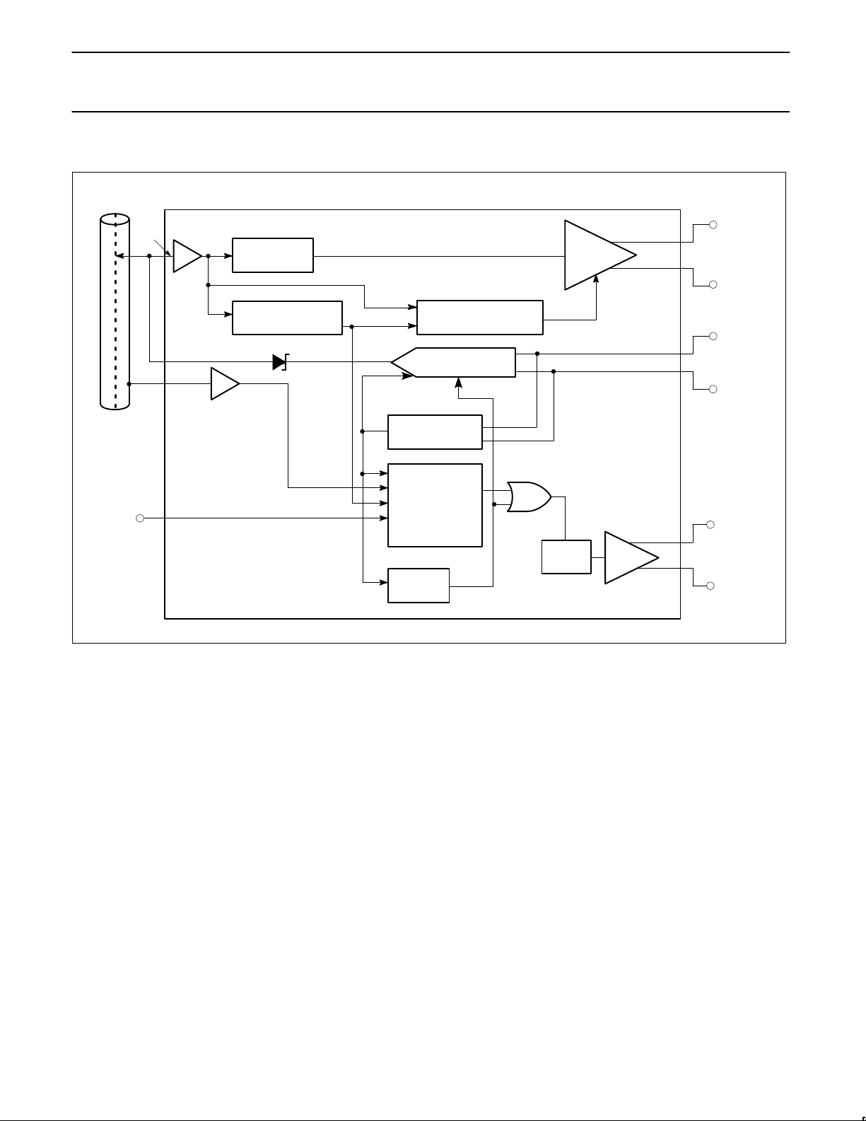
of a receiver, transmitter, receive-mode collision detector, heartbeat
generator and jabber timer (see Block Diagram). The transmitter
output connects directly to a doubly terminated 50Ω cable, while the
receiver output, collision detector output and transmitter input are
connected to the DTE through isolation transformers. Isolation
between the CTI and the DTE is an IEEE 802.3 requirement that
can be met on signal lines by using a set of pulse transformers
normally available in a standard 16-pin DIP. Power isolation for the
CTI is achieved using DC-to-DC conversion through a power
transformer (see Figure 1, Connection Diagram).
During transmission the jabber timer is initiated to disable the CTI
transmitter in the event of a longer than legal length data packet.
Receive-mode collision detection circuitry monitors the signals on
the coaxial cable to determine the presence of colliding packets and
signals the DTE in the event of a collision. At the end of every
transmission the heartbeat generator creates a pseudo collision for
a short time to ensure that the collision circuitry is functioning
correctly. The heartbeat function can be disabled for repeater
applications.
The CTI is normally part of a three chip set that implements a
complete Ethernet/ Thin Ethernet network interface for a DTE (see
Figure 2, Interface Diagram). The other chips are a Serial Network
Interface (SNI) and a Network Interface Controller (NIC). The SNI
provides Manchester Encoding and Decoding while the NIC handles
the media access protocol and buffer management tasks.
FEATURES
•Compatible with Ethernet II IEEE 802.3 10base5 and 10base2,
and ISO 8802/3 interface specifications
•100% drop-in compatible with industry standard 8392 sockets
•Integrates all transceiver electronics except signal and power
isolation
•Only one external resistor required for setting coaxial signaling
current
•Jabber timer function integrated on chip
•Heartbeat generator can be externally disabled for operation as
IEEE 802.3 compatible repeaters
PIN CONFIGURATION
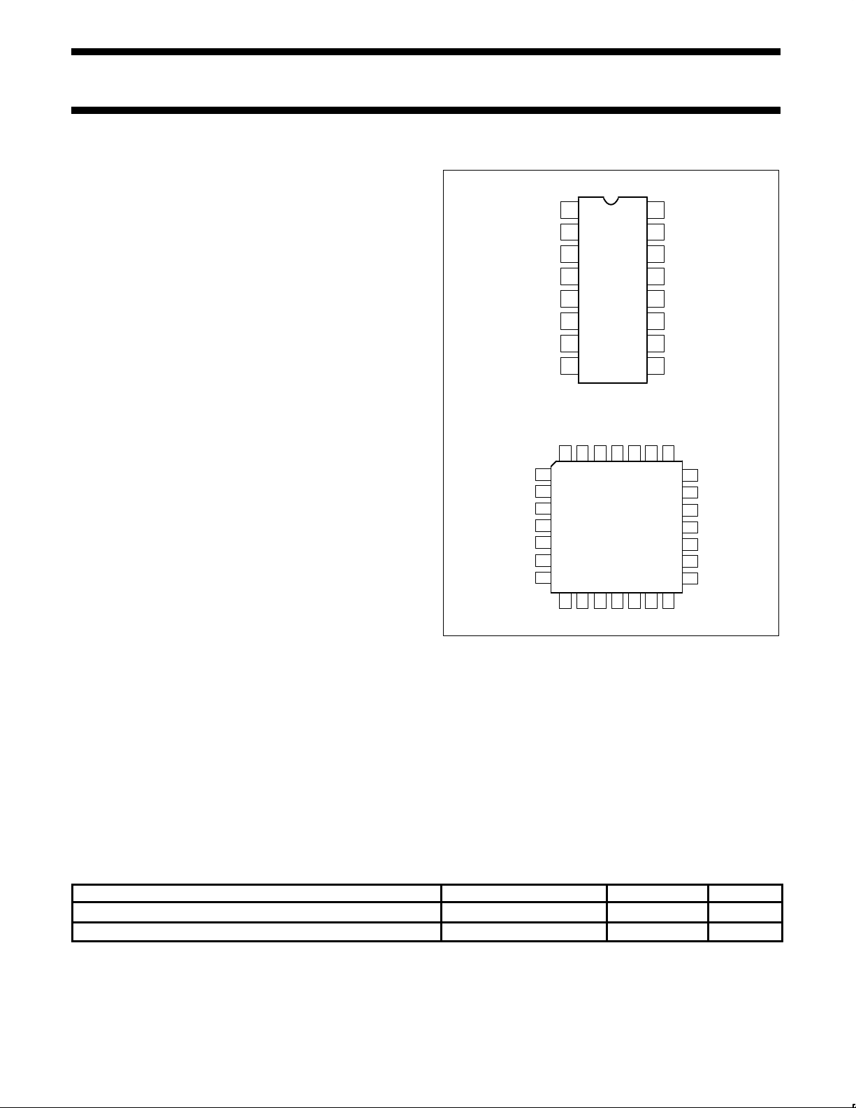
CD+ 1
CD– 2
RX+ 3
V
EE
4
V
EE
5
RX– 6
TX+ 7
TX– 8
16 CDS
15 TXO
14 RXI
13 V
EE
12 RR–
11 RR+
10 GND
9 HBE
N PACKAGE
1234
5
6
7
8
9
10
11
12 13 14 15 16 17 18
19
20
21
22
23
24
25
262728
V
EE
V
EE
V
EE
V
EE
V
EE
V
EE
V
EE
V
EE
V
EE
V
EE
V
EE
V
EE
V
EE
RR–
RX+
CD–
CD+
CDS
TXO
N/C
RXI
RX–
TX+
TX–
HBE
GND
GND
RR+
A PACKAGE
SD00283
•On-chip precision voltage reference for receive mode collision
detection
•Squelch circuitry on all signal inputs rejects noise
•Full ESD protection
•Standard 16-pin DIP and 28-pin PLCC packages
•Power-on reset prevents glitches on coaxial cable during power
up.
•Also available in advanced low-power BiCMOS technology. (See
selection chart and data sheets for the NE83C92, NE83Q92 or
NE83Q93 for appropriate optimal usages)
ORDERING INFORMATION
DESCRIPTION TEMPERATURE RANGE ORDER CODE DWG #
16-Pin Plastic Dual In-Line Package (DIP)
0 to +70°C
NE8392CN SOT28-4
28-Pin Plastic Lead Chip Carrier (PLCC)
0 to +70°C
NE8392CA SOT261-3

Philips Semiconductors Product specification
NE8392CCoaxial transceiver interface for Ethernet/Thin Ethernet
1995 May 1
2
PIN DESCRIPTIONS
PIN NO.
N PKG
PIN NO.
PLCC
SYMBOL DESCRIPTION
1
2
2
3
CD+
CD–
Collision Outputs. Balanced differential line driver outputs which send a 10MHz oscillation signal to
the DTE in the event of a collision, jabber interrupt or heartbeat test.
3
6
4
12
RX+
RX–
Receiver Outputs. Balanced differential line driver outputs which send the received signal to the
DTE.
7
8
13
14
TX+
TX–
Transmitter Inputs. Balanced differential line receiver inputs which accept the transmission signal
from the DTE and apply it to the coaxial cable at TXO once it meets Tx squelch threshold.
9 15 HBE
Heartbeat Enable. The heartbeat function is disabled when this pin is connected to VEE and enabled
when connected to GND or left floating.
11
12
18
19
RR+
RR–
External Resistor. A 1kΩ (1%) resistor connected between these pins establishes the signaling
current at TXO. RR– is internally connected to V
EE
.
14 26 RXI
Receiver Input. This pin is connected directly to the coaxial cable. Received signals are equalized,
amplified, and sent to the DTE through the RX+ pins once it meets Rx squelch threshold.
15 28 TXO
Transmitter Output. This pin is connected directly (Thin Ethernet) or through an external isolating
diode (Ethernet) to the coaxial cable.
16 1 CDS
Collision Detect Sense. Ground sense connection for the collision detection circuitry. This pin
should be directly connected to the coaxial cable shield to prevent ground drops affecting the
collision threshold voltage.
10
16
17
GND Positive Supply Pin.
4
5
13
5 to 11
20 to 25
V
EE
Negative supply pins. These pins also serve as a low thermal resistance path for extracting heat
from the die. They should, therefore, be connected to a large metal area on the PC board.
NOTE:
1. The IEEE 802.3 name for CD is CI; for RX is DI; for TX is DO.
ABSOLUTE MAXIMUM RATINGS
SYMBOL PARAMETER RATING UNIT
V
EE
Supply voltage
1
–12 V
V
IN
Voltage at any input
1
0 to –12 V
T
STG
Storage temperature range –65 to +150
°C
T
SOLD
Lead soldering temperature (10sec.) +300
°C
T
J
Recommended max junction temperature
2
+130
°C
θ
JA
Thermal impedance (N and A packages) 60
°C/W
NOTE:
1. 100% measured in production.
2. The junction temperature is calculated from the following expression:
T
J
= TA + θ
JA
[VEE (0.08 + n x 0.05/100) + 8(VEE –2) / R]
where
T
A
= Ambient temperature in °C.
θ
JA
= Thermal resistance of package.
V
EE
= Normal operating supply voltage in volts.
n = Percentage transmitter duty cycle.
R = Pull down resistors on the RX and CD pins in Ω.
The N package is specially designed to have a low θ
JA
by directly connecting the four center Pins 4, 5, 12, and 13 to the die attachment area.
These four pins then provide a conductive heat flow path from the die to the PCB where they should be soldered to a large area V
EE
track. For
the A package, Pins 5 to 11 and 19 to 25 should similarly be soldered to a large area V
EE
and rack.

Philips Semiconductors Product specification
NE8392CCoaxial transceiver interface for Ethernet/Thin Ethernet
1995 May 1
3
BLOCK DIAGRAM
RECEIVER
AC–DC SQUELCH
TRANSMITTER
TRANSMITTER
SQUELCH
COLLISION
COMPARATOR
&
HEARTBEAT
GENERATOR
JABBER
TIMER
RECEIVER
EQUALIZER
4–POLE BESSEL
LOW PASS FILTER
SENSE
BUFFER
10MHz
OSC
LINE
DRIVER
COAX
CABLE
BUFFER
LINE
DRIVER
HEARTBEAT ENABLE
COLLISION
PAIR
(CD+, CD–)
TRANSMIT
PAIR
(TX+, TX–)
RECEIVE
PAIR
(RX+, RX–)
DTE
INTERFACE
RXI
TXO
CDS
SD00274
 Loading...