

Page 1

Colour television Chassis
EM1.1A
AA
CL 36532061_000.eps
280803
Contents Page Contents Page
1 Technical Specifications, Connections, and Chassis
Overview 2
2 Safety Instructions, Warnings, and Notes 4
3 Directions for Use 6
4 Mechanical Instructions 7
5 Service Modes, Error Codes, and Faultfinding 11
6 Block Diagrams, Testpoint Overviews, and
Waveforms
Wiring Diagram 17
Block Diagram LSP Supply and Deflection 18
Testpoint Overview LSP and CRT 19
Block Diagram Video 20
Testpoint Overview SSB 21
Block Diagram Audio 22
2
I
C Overview 23
Supply Lines Overview 24
7 Circuit Diagrams and PWB layouts Diagram PWB
Large Signal Panel (Diagram A1-11)25-34 35-41
Large Signal Panel (FL13B) (Diagram A1-11)42-51 52-57
Small Signal Board (Diagram B1-7) 58-63 64-73
Small Signal Board (FL13B) (Diagram B1-6) 74-78 79-80
Side I/O Panel (Diagram D) 81 82
CRT Panel (Diagram F) 83 84
CRT Panel (FL13B) (Diagram F) 85 86
DC Shift Panel (Diagram G) 87 87
VDAF + 2nd Orders (Diagram I) 88 89
VDAF + 2nd Orders (FL13B) (Diagram I) 90 91
Mains Switch (FL9) (Diagram J) 92 93
Mains Switch (PV2) (Diagram J) 94 94
Mains Switch (FL13B) (Diagram J) 95 96
HD Jack Panel (Diagram N1-4) 97-99 100-102
HD Jack Panel (FL13B) (Diagram N1-4) 103-105 106
Side I/O Panel (Diagram O) 107 108
Side I/O Panel (FL13B) (Diagram O) 109 110
©
Copyright 2004 Philips Consumer Electronics B.V. Eindhoven, The Netherlands.
All rights reserved. No part of this publication may be reproduced, stored in a
retrieval system or transmitted, in any form or by any means, electronic,
mechanical, photocopying, or otherwise without the prior permission of Philips.
Top Control Panel (PV2) (Diagram P) 111 112
Top Control Panel (PV0) (Diagram P) 111 113
Top Control Panel (FL13B) (Diagram P) 114 115
8 Alignments 117
9 Circuit Descriptions 122
List of Abbreviations 136
IC Data Sheets 138
10 Spare Parts List 140
11 Revision List 148
Published by BB 0472 Service PaCE Printed in the Netherlands Subject to modification EN 3122 785 13871
Page 2
EN 2 EM1.1A AA1.
Technical Specifications, Connections, and Chassis Overview
1. Technical Specifications, Connections, and Chassis Overview
Index of this chapter:
1.1 Technical Specifications
1.2 Connections
1.3 Chassis Overview
1.1 Technical Specifications
1.1.1 Reception
Tuning system : PLL
Color systems (off-air) : PAL B/G/D/K/I/M/N,
Sound systems : FM/FM,
: 2SC B/G,
: NICAM B/G/D/K/I/L
A/V connections : PAL B/G,
Channel selections : 100 channels,
: UVSH-channels
Frequency range : 44.25 - 855.25 MHz
Aerial input : 75 ohm, Coax
1.1.2 Miscellaneous
AC voltage : 160 - 276 V (± 10 %),
AC frequency : 50 / 60 Hz (± 5%)
Ambient temperature : + 5 to + 45 deg. C.
Standby Power consumption : 1 W
1.2 Connections
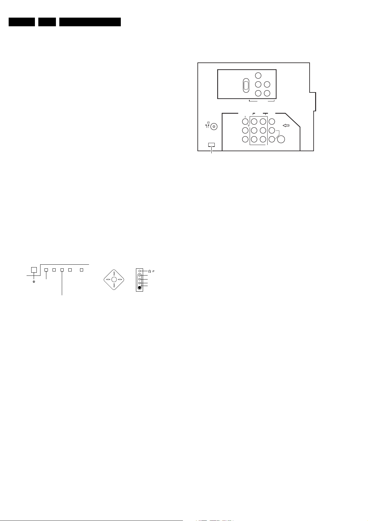
1.2.1 Front and Top Controls / Side Connections
P/CH+
'IR-
RECEIVER'
SK 1
LED
Figure 1-1 Front/Top controls and Side I/O
S-Video
1 - Gnd H
2 - Gnd H
3 -Y 1 Vpp / 75 ohm j
4 -C 0.3 Vpp / 75 ohm j
Audio / video
- - Video 1 Vpp / 75 ohm jq
- - Audio L (0.5 Vrms / 10 kohm) jq
- - Audio R (0.5 Vrms / 10 kohm) jq
- - Headphone
(3.5mm) (32 - 2000 ohm / 10 mW) rt
M
P/CH-
V+V-
3.5
AUDIO R
AUDIO L
VIDEO
SVHS
CL26532072_009.eps
140602
Rear Connections
Y
75
9
SERVICE
CONNECTOR
(COMPAIR)
RGB
MONITOR
OUT
AUDIO
Pb
Pr
VIDEO 2FH - 480p/1080i
V
L
R
AV3 IN
AV1
AV2
IN
IN
Y
PbPrLRL
L
R
CL 36532061_043.eps
R
VIDEO
AUDIO
S-VIDEO
030903
Figure 1-2 Rear View
Monitor out
1 - Video 1 Vpp / 75 ohm kq
2 - Audio L (0.5 Vrms / 10 kohm) kq
3 -Audio R (0.5 Vrms / 10 kohm) kq
AV1 in
1 - Y 0.7 Vpp / 75 ohm jq
2 - Pb 0.7 Vpp / 75 ohm jq
3 - Pr 0.7 Vpp / 75 ohm jq
AV1 in
4 - Video 1 Vpp / 75 ohm jq
5 - Audio L (0.5 Vrms / 10 kohm) jq
6 -Audio R (0.5 Vrms / 10 kohm) jq
AV2 in
1 - Video 1 Vpp / 75 ohm jq
2 - Audio L (0.5 Vrms / 10 kohm) jq
3 -Audio R (0.5 Vrms / 10 kohm) jq
AV2 in (SVHS)
1 - Gnd H
2 - Gnd H
3 - Y 1 Vpp / 75 ohm j
4 - C 0.3 Vpp / 75 ohm j
AV3 in (D-sub connector)
1 - Pr (R) 0.35 Vpp (0.7 Vpp) / 75 ohm jq
2 - Y (G) 0.7 Vpp (0.7 Vpp) / 75 ohm jq
3 - Pb (B) 0.35 Vpp (0.7 Vpp) / 75 ohm jq
4 - H 5 Vpp / 1 kohm jq
5 - V 5 Vpp / 1 kohm jq
AV3 in (cinches)
1 - Y (G) 0.7 Vpp (0.7 Vpp) / 75 ohm jq
2 - Pb (B) 0.35 Vpp (0.7 Vpp) / 75 ohm jq
3 - Pr (R) 0.35 Vpp (0.7 Vpp) / 75 ohm jq
AV3 in
1 - Audio L (0.5 Vrms / 10 kohm) jq
2 -Audio R (0.5 Vrms / 10 kohm) jq
Page 3
Technical Specifications, Connections, and Chassis Overview
1.3 Chassis Overview
EN 3EM1.1A AA 1.
&
SIDE I/O PANEL
OD
JACK HIGH
N
DEFINITION INTERFACE
Figure 1-3 PWB location
TOP CONTROL PANEL
TOP CONTROL PANEL
SMALL SIGNAL BOARD
MAINS SWITCH (PV2 & FL9)
LARGE SIGNAL PANEL
VDAF + 2nd ORDERS PANEL
(styling FL9)
(styling PV2)
CRT/SCAVEM PANEL
DC-SHIFT (optional)
CL 36532061_042.eps
or
020903
P
P
P
P
F
B
P
J
A
G
I
Page 4
EN 4 EM1.1A AA2.
Safety Instructions, Warnings, and Notes
2. Safety Instructions, Warnings, and Notes
2.1 Safety Instructions
Index of this chapter:
2.1 Safety Instructions
2.2 Maintenance Instructions
2.3 Warnings
2.4 Notes
Safety regulations require that during a repair:
• Due to the chassis concept, a very large part of the chassis
(including horizontal and vertical deflection) is 'hot.'
Connect the set to AC power via an isolation transformer.
• Safety components, indicated by the symbol h, must be
replaced with original PCEC components.
• Wear safety goggles when you replace the CRT.
Safety regulations require that after a repair, you must return
the set in its original condition. Pay particular attention to the
following points:
• General repair instruction: as a strict precaution, we advise
you to resolder the solder connections through which the
horizontal deflection current is flowing, in particular:
1. All pins of the line output transformer (LOT.)
2. Flyback capacitor(s.)
3. S-correction capacitor(s.)
4. Line output transistor.
5. Pins of the connector with wires to the deflection coil.
6. Other components through which the deflection current
flows.
Note: This resoldering is advised to prevent bad connections
due to metal fatigue in solder connections and is therefore only
necessary for television sets more than two years old.
• Route the wire trees and EHT cable correctly and secure
them with the mounted cable clamps.
• Check the insulation of the AC power cord for external
damage.
• Check the strain relief of the AC power cord for proper
function, to prevent the cord from touching the CRT, hot
components, or heat sinks.
• Check the electrical DC resistance between the AC plug
and the secondary side (only for sets that have an isolated
power supply.) To do this:
1. Unplug the AC power cord and connect a wire between
the two pins of the AC plug.
2. Set the AC power switch to the “on” position (keep the
AC power cord unplugged.)
3. Measure the resistance value between the pins of the
AC plug and the metal shielding of the tuner or the
aerial connection of the set. The reading should be
between 4.5 Mohm and 12 Mohm.
• Check the cabinet for defects, to prevent the customer from
touching any inner parts of the television set.
3. Clean the picture tube panel and the neck of the picture
tube.
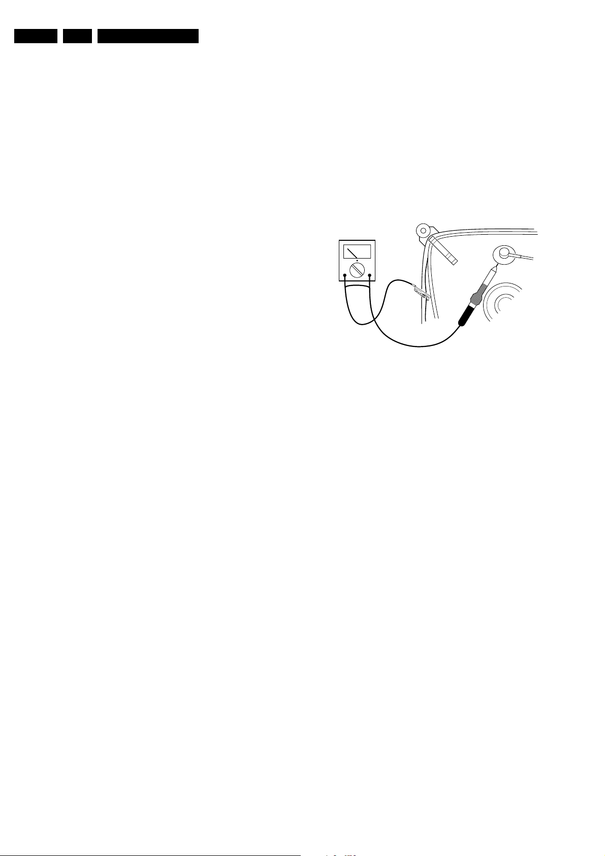
2.3 Warnings
• In order to prevent damage to ICs and transistors, avoid all
high voltage flashovers. In order to prevent damage to the
picture tube, use the method shown in Fig. 2-1 to discharge
the picture tube. Use a high voltage probe and a multimeter
(position Vdc.) Discharge until the meter reading is 0 V
(after approx. 30s.)
V
Figure 2-1 Discharge picture tube
• All ICs and many other semiconductors are susceptible to
electrostatic discharges (ESD. w) Careless handling
during repair can reduce life drastically. When repairing,
make sure that you are connected with the same potential
as the mass of the set by a wristband with resistance. Also
keep components and tools at this potential.
• Available ESD protection equipment:
– Complete kit ESD3 (small table mat, wristband,
connection box, extension cable, and ground cable)
4822 310 10671.
– Wristband tester 4822 344 13999.
• Together with the deflection unit and any multi-pole unit,
flat square picture tubes form an integrated unit. The
deflection and the multi-pole units are set optimally at the
factory. Adjustment of this unit during repair is therefore not
recommended.
• Be careful during measurements in the high voltage
section and on the picture tube.
• Never replace modules or other components while the unit
is switched “on.”
• When you align the set, use plastic rather than metal tools.
This will prevent any short circuits and the danger of a
circuit becoming unstable.
CL96532156_040.eps
140501
2.2 Maintenance Instructions
It is recommended to have a maintenance inspection carried
out by qualified service personnel. The interval depends on the
usage conditions:
• When the set is used under normal circumstances, for
example in a living room, the recommended interval is
three to five years.
• When the set is used in an environment with higher dust,
grease or moisture levels, for example in a kitchen, the
recommended interval is one year.
• The maintenance inspection includes the following actions:
1. Perform the “general repair instruction” noted above.
2. Clean the power supply and deflection circuitry on the
chassis.
2.4 Notes
2.4.1 General
• Measure the voltages and waveforms with regard to the
chassis (= tuner) ground (H), or hot ground (I), depending
on the area of circuitry being tested.
• The voltages and waveforms shown in the diagrams are
indicative. Measure them in the Service Default Mode with
a color bar signal and stereo sound (L: 3 kHz, R: 1 kHz;
unless stated otherwise) and picture carrier at 61.25 MHz
(NTSC, channel 3.)
• Where necessary, measure the waveforms and voltages
with (D) and without (E) aerial signal. Measure the
voltages in the power supply section both in normal
operation (G) and in standby (F.) These values are
indicated by means of the appropriate symbols.
Page 5

Safety Instructions, Warnings, and Notes
EN 5EM1.1A AA 2.
• The picture tube panel has printed spark gaps. Each spark
gap is connected between an electrode of the picture tube
and the Aquadag coating.
• The semiconductors indicated in the circuit diagram and in
the parts lists are interchangeable per position with the
semiconductors in the unit, irrespective of the type
indication on these semiconductors.
• DOLBY, the double D symbol and PRO LOGIC are
trademarks of Dolby Laboratories Licensing Corporation.
Manufactured under license from Dolby Laboratories
Licensing Corporation.
Figure 2-2 Dolby Pro Logic Symbol
2.4.2 Schematic Notes
• All resistor values are in ohms and the value multiplier is
often used to indicate the decimal point location (e.g. 2K2
indicates 2.2 kOhm).
• Resistor values with no multiplier may be indicated with
either an "E" or an "R" (e.g. 220E or 220R indicates 220
Ohm).
• All Capacitor values are expressed in Micro-Farads (µ =
-6
x10
), Nano-Farads (n = x10-9), or Pico-Farads (p = x10
12
).
• Capacitor values may also use the value multiplier as the
decimal point indication (e.g. 2p2 indicates 2.2 pF).
• An "asterisk" (*) indicates component usage varies. Refer
to the diversity tables for the correct values.
• The correct component values are listed in the Electrical
Replacement Parts List. Therefore, always check this list
when there is any doubt.
2.4.3 Lead Free Solder
Philips CE is going to produce lead-free sets (PBF) from
1.1.2005 onwards.
Lead-free sets will be indicated by the PHILIPS-lead-free logo
on the Printed Wiring Boards (PWB):
P
b
Figure 2-3 Lead-free logo
This sign normally has a diameter of 6 mm, but if there is less
space on a board also 3 mm is possible.
In case of doubt wether the board is lead-free or not (or with
mixed technologies), you can use the following method:
• Always use the highest temperature to solder, when using
SAC305 (see also instructions below).
• De-solder thoroughly (clean solder joints to avoid mix of
two alloys).
Caution: For BGA-ICs, you must use the correct temperatureprofile, which is coupled to the 12NC. For an overview of these
profiles, visit the website www.atyourservice.ce.philips.com
(needs subscription, but is not available for all regions)
You will find this and more technical information within the
"Magazine", chapter "Workshop information".
For additional questions please contact your local repairhelpdesk.
Due to lead-free technology some rules have to be respected
by the workshop during a repair:
• Use only lead-free soldering tin Philips SAC305 with order
code 0622 149 00106. If lead-free solder paste is required,
please contact the manufacturer of your soldering
equipment. In general, use of solder paste within
workshops should be avoided because paste is not easy to
store and to handle.
• Use only adequate solder tools applicable for lead-free
soldering tin. The solder tool must be able
– To reach at least a solder-tip temperature of 400°C.
– To stabilise the adjusted temperature at the solder-tip.
– To exchange solder-tips for different applications.
• Adjust your solder tool so that a temperature around 360°C
- 380°C is reached and stabilised at the solder joint.
Heating time of the solder-joint should not exceed ~ 4 sec.
Avoid temperatures above 400°C, otherwise wear-out of
tips will rise drastically and flux-fluid will be destroyed. To
avoid wear-out of tips, switch “off” unused equipment or
reduce heat.
• Mix of lead-free soldering tin/parts with leaded soldering
tin/parts is possible but PHILIPS recommends strongly to
avoid mixed regimes. If not to avoid, clean carefully the
solder-joint from old tin and re-solder with new tin.
• Use only original spare-parts listed in the Service-Manuals.
Not listed standard material (commodities) has to be
purchased at external companies.
-
• Special information for lead-free BGA ICs: these ICs will be
delivered in so-called "dry-packaging" to protect the IC
against moisture. This packaging may only be opened
short before it is used (soldered). Otherwise the body of the
IC gets "wet" inside and during the heating time the
structure of the IC will be destroyed due to high (steam)pressure inside the body. If the packaging was opened
before usage, the IC has to be heated up for some hours
(around 90°C) for drying (think of ESD-protection !).
Do not re-use BGAs at all!
• For sets produced before 1.1.2005, containing leaded
soldering tin and components, all needed spare parts will
be available till the end of the service period. For the repair
of such sets nothing changes.
2.4.4 Practical Service Precautions
• It makes sense to avoid exposure to electrical shock.
While some sources are expected to have a possible
dangerous impact, others of quite high potential are of
limited current and are sometimes held in less regard.
• Always respect voltages. While some may not be
dangerous in themselves, they can cause unexpected
reactions - reactions that are best avoided. Before reaching
into a powered TV set, it is best to test the high voltage
insulation. It is easy to do, and is a good service precaution.
• Before powering up the TV set with the back cover off
(or on a test fixture), attach a clip lead to the CRT DAG
ground and to a screwdriver blade that has a well insulated
handle. After the TV is powered on and high voltage has
developed, probe the anode lead with the blade, starting at
the case of the High Voltage Transformer (flyback - IFT.)
Move the blade to within two inches of the connector of the
CRT. If there is an arc, you found it the easy way,
without getting a shock! If there is an arc to the
screwdriver blade, replace the part which is causing the
problem; the High Voltage Transformer or the lead (if it is
removable.
Page 6

EN 6 EM1.1A AA3.
3. Directions for Use
You can download this information from the following websites:
http://www.philips.com/support
http://www.p4c.philips.com
Directions for Use
Page 7
4. Mechanical Instructions
Mechanical Instructions
EN 7EM1.1A AA 4.
Index of this chapter:
4.1 Service Connector (for ComPair)
4.2 Set Disassembly
4.3 Service Positions
4.4 Assembly / Board Removal
4.5 Set Reassembly
Note: Figures below can deviate slightly from the actual
product, due to different set designs.
4.1 Service Connector (for ComPair)
To perform service diagnostics with ComPair, it is not
necessary to disassemble the set. You simply have to connect
the ComPair interface box with the appropriate cable, to the
service connector. This connector is located on the rear of the
set behind a small plastic cover plate (see figure below.) Then
start the ComPair program (see chapter 5.)
4.2 Set Disassembly
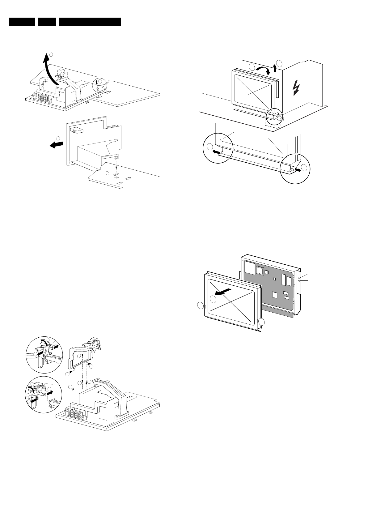
Follow the disassembly instructions below.
4.2.1 Back Cover Removal
3
4.3.1 Control-Jack-High-Definition-Interface Panel Solder Side
2
1
4
4
3
2
CL 26532072_013.eps
140602
Figure 4-2 Service position 1
To remove or access the “Control-Jack-High-DefinitionInterface” panel, do the following:
1. Remove screw [1.]
2. To release the peg, push it toward the CRT [2.] At the same
time use a screwdriver to release the clamp at the right side
of the bracket.
3. Now, pull the complete module away from the LSP [3.] It
hinges in the LSP bracket.
4. To remove the panel, remove the four panel screws [4.]
1
Figure 4-1 Rear Cover Removal
Warning: Disconnect the mains power cord before you remove
the back cover.
To access the electronics of the set, you must remove the back
cover:
1. Remove the screws [1] of the rear jack panel cover plate.
2. Remove the remaining screws [2] at the two sides, and the
top of the back cover.
3. Remove the back cover. Make sure that wires and cables
are not damaged while removing the cover.
4. Remove the rear jack panel cover plate by removing
screws [3.] Pull the plate backwards.
4.3 Service Positions
This chassis has several predefined service positions, for
better accessibility. They are explained below in more detail.
CL 26532072_012.eps
180602
12
4.3.2 LSP Component Side
SSB - bracket
1
2
SSB
LOT - bracket
LSP
1
2
Bottom tray
CL 26532072_018.eps
180602
Figure 4-3 Service position 2
To better access the component side of the LSP, do the
following (see figure above):
1. Remove the LSP bracket from the bottom tray by pulling it
backwards.
2. Hook the bracket in the first row of holes of the bottom tray.
In other words, reposition the bracket from [1] to [2.]
Page 8
EN 8 EM1.1A AA4.
Mechanical Instructions
4.3.3 LSP Solder Side
2
4
Figure 4-4 Service position 3
5. Now you can remove the complete bracket. Push it, at the
height of the LSP-bracket, towards the CRT [6] and lift it out
of the LSP-bracket [7.]
1
1
1502
SSB
3
2
2
3
CL 26532072_014.eps
180602
CL 26532072_016.eps
140602
Figure 4-6 SSB removal (part 2)
To access the bottom side (solder side) of the LSP, do the
following (see figure above):
1. Remove the DAF module (see paragraph “DAF Assembly/
Panel” below.)
2. To disconnect the degaussing coil from the LSP, remove
the cable from connector 1502 [1.]
3. Release the wires from their clamps to make room to
reposition the LSP.
4. Turn the LSP 90 degrees clockwise [2], and place it in the
hole at the left side of the bottom tray [3.]
4.3.4 Small Signal Board (SSB)
There is no predefined service position for the SSB. Most test
points are located on the A-side (the side that faces the tuner.)
If you have to replace ICs, you must take the complete SSB
module out of the SIMM-connector.
To access the SSB test points, do the following:
3
2
2
5
4
4
1
6
6
7
3
7
Figure 4-5 SSB removal (part 1)
1. Put the LSP in service position 2 (as described above.)
2. Remove the fixation screw, which holds the SSB-bracket
[1.]
3. Release the clamping jaw at the top of the SSB bracket [2]
and [3.]
4. Push the two clamping lugs outwards, and pull the top of
the bracket at the same time upwards [4] and [5.]
CL 26532072_015.eps
180602
1. Push the top of the SSB toward the LOT [1.]
2. Due to the pressure, the two metal clamps at both sides of
the SIMM-connector will release [2.]
3. Take the complete SSB out [3.]
2
1
1
Figure 4-7 SSB removal (part 3)
1. Once you have taken out the SSB, remove the A-side
shielding [2.] Sometimes it is necessary to unsolder some
solder tags before doing this [1.]
2. Replace the SSB module in the SIMM-connector in reverse
order.
Notes:
• For better access to the SSB, it is possible to order an
“extension board,” which is part number 9965 000 05769.
• If it is necessary for measurements, you can put the LSP in
“service position 3” (as described above.)
4.4 Assembly / Board Removal
Sometimes, it may be necessary to swap a complete assembly
or Circuit Board Assembly (CBA.) This procedure is explained
below.
SDM (4006)
SAM (4005)
CL 16532044_008.eps
090501
Page 9
Mechanical Instructions
EN 9EM1.1A AA 4.
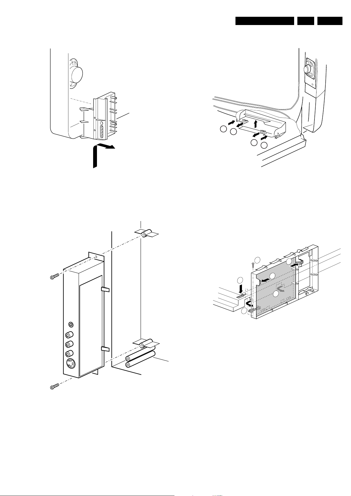
4.4.1 Top Control Assembly/Panel
CL 96532023_009.ai
Figure 4-8 Top control assembly
1. Remove the two fixation screws.
2. Pull the board backward.
4.4.2 Side-I/O Assembly and Panel
230399
4.4.3 Mains Switch Assembly/Panel
N
P
P
N
CL 96532023_010.ai
Figure 4-10 AC Power Switch / LED Panel
1. Release the fixation clamps by pushing them upward [1.]
2. At the same time, pull the complete assy backward [2.]
Note: Be aware that the degaussing coil may hamper this.
3. Now release the two fixation clamps [3], in order to remove
the print from its bracket [4.]
Note: If necessary, you can replace the light guide.
230399
CL 96532099_030.eps
200999
Figure 4-9 Top control assembly
1. Remove the fixation screws
2. Pull the assembly backward.
3. Release the cable from its clamp.
4. Release the two clamps on the front side of the bracket (the
board hinges at the back side.)
5. Remove the board from the bracket.
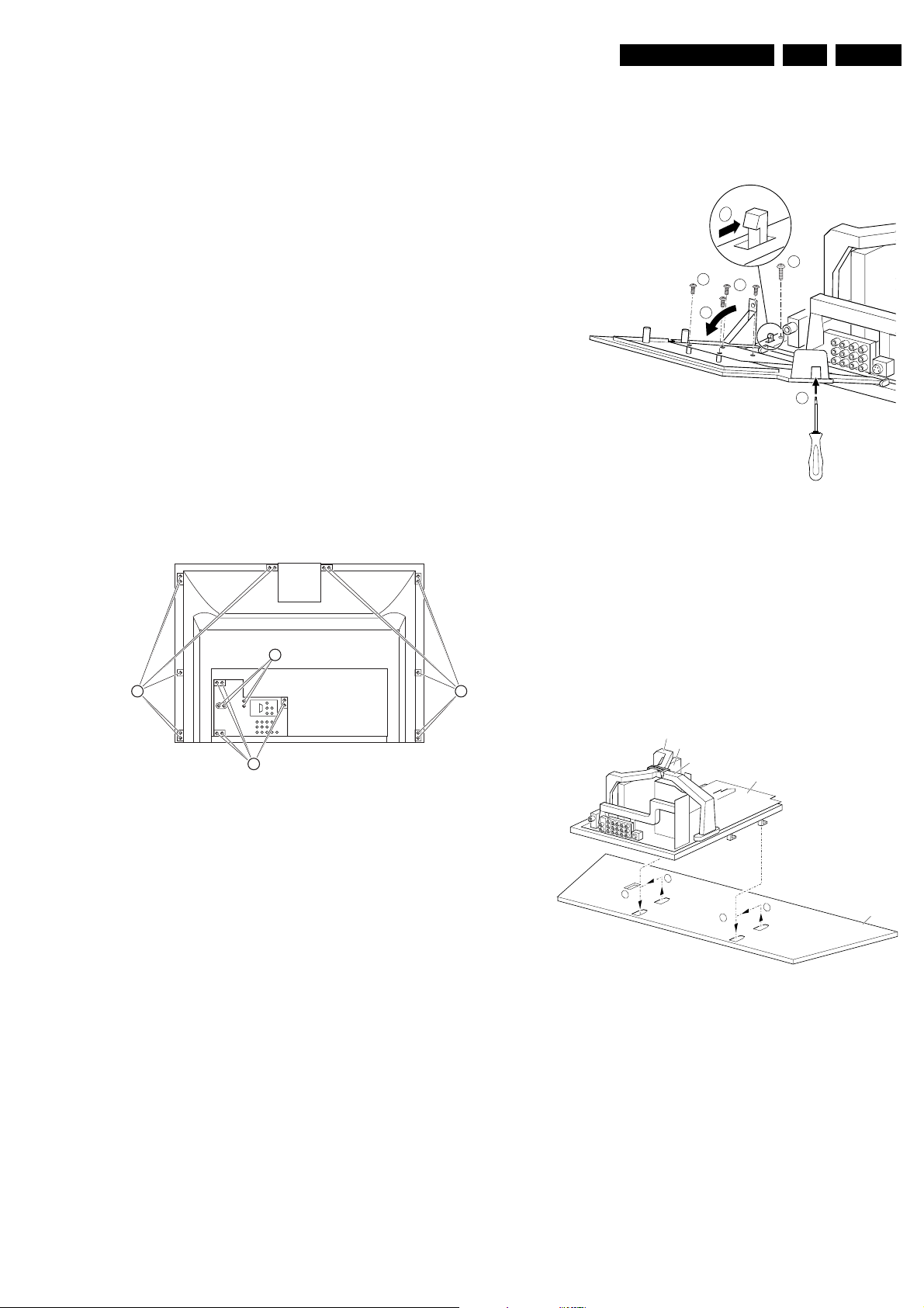
4.4.4 DAF Assembly/Panel
1
2
4
4
3
3
CL 16532044_011.eps
Figure 4-11 DAF module
1. Remove the screw [1] (if present.)
2. Push the clamp [2] down, and, at the same time, pull the
complete bracket away from the CRT [3.] The module is
now free from the LSP bracket.
3. Release the clamps [4], in order to remove the board from
its bracket.
4.4.5 Small Signal Board (SSB)
See section “Small Signal Board (SSB)” above.
4.4.6 Large Signal Panel (LSP)
1. Remove the SSB (see paragraph “Small Signal Board
(SSB)” above.)
2. Remove the DAF-module (see paragraph “DAF Assembly/
Panel” above.)
3. Disconnect the necessary cables.
4. Release the clamps on the left of the LSP-bracket (the
board hinges at the right side.)
5. Remove the board from the bracket.
150501
Page 10

EN 10 EM1.1A AA4.
4.5 Set Reassembly
To reassemble the set, perform all disassembly processes in
reverse order.
Before replacing the back cover:
• Be sure the mains power cord is mounted correctly in its
guiding brackets.
• Be sure all wires/cables are returned to their original
positions. This is very important due to the large “hot” area
of the set
Mechanical Instructions
Page 11

Service Modes, Error Codes, and Fault Finding
5. Service Modes, Error Codes, and Fault Finding
EN 11EM1.1A AA 5.
Index of this chapter:
5.1 Test conditions
5.2 Service Modes
5.3 Problems and Problem Solving Tips
5.4 ComPair
5.5 Error Buffer
5.6 The 'Blinking LED' Procedure
5.7 Protections
5.8 General tips and repair tips
5.1 Test conditions
Perform measurements under the following conditions:
• Service mode: SDM (Service Default Mode).
• Video: color bar signal.
• Audio: 1kHz, mono.
5.2 Service Modes
The Service Default Mode (SDM) and Service Alignment Mode
(SAM) offer several features for the service technician, while
the Customer Service Menu (CSM) is used for communication
between the servicer and the customer.
There is also the option of using ComPair, a hardware interface
between a computer (see requirements below) and the TV
chassis. It offers the ability of structured troubleshooting, error
code reading, and software version readout for this chassis.
Minimum requirements: a 486 processor, Windows 3.1 and a
CD-ROM drive (see 'ComPair' section).
5.2.1 Service Default Mode (SDM)
Purpose
• Provide a situation with predefined settings in order to
retrieve the same measurement results as published in this
manual.
• Start the “blinking LED” sequence procedure.
• Have the possibility to override the 5V protection.
Specifications
• Tuning frequency: 475.25 MHz for PAL.
• Colour system: PAL B/G.
• All picture settings at 50% (brightness, color, picture).
• All sound settings at 50% except volume at 25% (bass,
treble, and balance at 50%, volume at 25%).
• All service-unfriendly modes (if present) are disabled, such
as:
– (sleep) timer,
– child/parental lock,
– blue mute,
– hotel/hospitality mode,
– auto switch-off (when no video signal is received for 15
minutes),
– skip/blank of non-favorite presets/channels,
– auto store of personal presets,
– auto user menu time-out.
How to enter SDM
Use one of the following methods:
• Press the following key sequence on the remote control
transmitter:
• 0-6-2-5-9-6-MENU Do not allow the display to time out
between entries while keying the sequence.
Note: It is possible that the main menu will appear when
entering SDM. To switch it off, push the ‘MENU’ button
again.
• Via ComPair (simulating the DST).
• Via short-circuiting the solder pads on the SSB (next to
connector 1304). Disconnect the set from the mains, short
circuit pads, then reconnect the set to the mains.
Caution: Entering SDM by short-circuiting the solder pads on
the SSB will override the 5V protection. This should only be
done for a short period. In case of SW protections (errors 1,2,4
and 8), the set will shut down in 15 seconds.
When doing this, the service technician must know what
he is doing, as it could lead to damaging the set.
After entering SDM, 'SDM' will appear at the upper right corner
of the screen for recognition.
How to navigate in SDM
When you press the 'MENU' button on the remote control
transmitter, the set toggles between the SDM and the normal
user menus (with the SDM mode still active in the background).
When you press the 'STATUS/EXIT' button on the remote
control transmitter, the set shows/hides the error buffer. To
prevent interference with oscilloscope measurements, it is
possible to hide the OSD.
How to exit SDM
Switch the set to STANDBY by pressing the ‘POWER’ button
on the remote control transmitter or press the 'POWER' switch
on the set.
5.2.2 Service Alignment Mode (SAM)
Purpose
• To perform alignments.
• To change option settings.
• To display/clear the error code buffer.
Specifications
• Software alignments.
• Option settings.
• Error buffer reading and erasing. The most recent error
code is displayed on the left side.
• Hours counter (in hexadecimal format)
• Software version.
How to enter SAM
Use one of the following methods:
• Press the following key sequence on the remote control
transmitter:
• 0-6-2-5-9-6-STATUS/EXIT Do not allow the display to time
out between entries while keying the sequence.
• Via ComPair (simulating the dealer remote).
• By using the 'ALIGN' button on the dealer remote while the
set is in normal operation mode.
• Via short-circuiting the solder pads on the SSB (next to
connector 1304). Disconnect the set from the mains, short
circuit pads, then reconnect the set to the mains. The set
will startup in SDM, press 0-6-2-5-9-6-STATUS/EXIT to
switch to SAM.
After entering SAM, 'SAM’ will appear at the upper right corner
of the screen for recognition.
Explanation of SAM menu
The Service Alignment Mode menu will now appear on the
screen. The following information is displayed:
1. ‘Operation hours’ timer (hexadecimal)
2. Software identification of the main microprocessor
(AAABBC-X.Y, example: EM12U1-1.0)
• AAA is the chassis name.
Page 12

EN 12 EM1.1A AA5.
Service Modes, Error Codes, and Fault Finding
• BB = Software code belonging to a certain stroke
number.
• C = language cluster number.
• X = main software version number.
• Y = software sub-version number.
3. Error buffer (7 errors possible).
4. Option bytes (8 codes possible); options are explained
below.
5. Sub menus are listed in a scroll menu.
How to navigate in SAM
Select menu items with the 'MENU UP/DOWN' keys. This will
highlight the selected item. When not all menu items fit on the
screen, use the 'MENU UP/DOWN' keys to display the next/
previous menu items.
With the 'MENU LEFT/RIGHT' keys, it is possible to:
• (De)activate the selected menu item (for example, SERVBLK).
• Change the value of the selected menu item (for example,
VER-SLOPE).
• Activate the selected sub menu (for example,
GEOMETRY).
Pressing the 'MENU/SELECT' button on the remote control
transmitter switches between the SAM and the normal user
menus (with the SAM mode still active in the background).
Press the 'MENU/SELECT' key in a sub menu to return to the
previous menu.
How to exit SAM
Switch the set to STANDBY by pressing the power button on
the remote control transmitter or press the 'POWER' switch on
the set.
5.2.3 Customer Service Mode (CSM)
Purpose
When a customer is having problems with his TV set, the
service technician can ask the customer to activate the CSM,
in order to identify the status of the set. Now, the service
technician can judge the severity of the complaint. In many
cases, he can advise the customer how to solve the problem,
or he can decide if it is necessary to visit the customer.
The CSM is a read only mode; therefore, modifications are not
possible in this mode.
How to enter CSM
The CSM will be turned on after pressing the ‘MUTE’ key on the
remote control transmitter and any of the control buttons on the
TV for at least 4 seconds simultaneously. This activation only
works if there is no menu on the screen.
Line 1:
HRS: Hexadecimal counter of operating hours. Example: 1B
(hex)= 0001 1011 (binary)= 27 (decimal).
Standby hours are not counted as operating hours.
Note: every time the set is turned on, the counter will advance
one hour.
SWID: Software identification of the main microprocessor (see
explanation of software version in the “Service Alignment
Mode” section).
Line 2:
Error code buffer (for more details see “Error buffer” section).
Displays the last 7 errors of the error code buffer.
Line 3:
Option bit setting controls the software and hardware
functionality. An option byte or option number represents 8 of
those bits. Each option number is displayed as a decimal
number between 0 and 255. The set may not work correctly
when an incorrect option code is set. See “Alignments” section
for more information on correct option settings.
Line 4:
Not valid in this set. No message here.
Line 5:
Indicates that the set is not receiving a signal on the selected
source.
Note: On some models, BLUE MUTE is displayed (if the BLMU
option is ON) when no signal is received.
If there is no signal, 'NO SIGNAL' is displayed.
Line 6:
Indicates whether the SLEEPTIMER function is ON/OFF. This
is displayed by 'TIMER ON.'
Line 7:
Indicates whether the CHILD LOCK function is ON/OFF. This
is displayed by 'CHANNEL LOCKED.'
Line 8:
Indicates whether the current channel is defined as SKIPPED
or NOT PREFERRED.
Line 9:
Not valid.
Line 10:
Indicates the source at entry to CSM: Channel number or
External source name (AV1, AV2, AV3, AV4, CVI).
Line 11:
Indicates which sound mode is installed for this channel: Mono,
Stereo, or SAP.
Line 12 to 17:
Values indicate parameter levels of volume, balance, hue,
color, brightness, and picture at CSM entry.
How to exit CSM
The Customer Service Mode will switch off after pressing any
key on the remote control transmitter (except the 'channel +' or
'channel -' key) or turning off the TV set with the 'POWER'
button on the remote control transmitter or the television set.
5.3 Problems and Problem Solving Tips
5.3.1 Picture Problems
TV switches off or changes channel without any user action
The TV set switches off after 'TV SWITCHING OFF' was
displayed.
Auto standby switched the set off because:
• There was no signal identification signal for more than 15
minutes.
• There was no remote control transmitter signal received or
local key pressed for over 2 hours.
See “Alignments” section for a description of the options to
enable/disable auto standby (option SBNP).
Picture too dark or too bright
• Press the 'Smart Picture' button on the remote control
transmitter. If the picture improves, increase/decrease the
brightness value or increase/decrease the contrast value.
• If the picture is OK after entering Customer Service Mode,
increase/decrease the brightness value or increase/
decrease the contrast value.
Page 13

Service Modes, Error Codes, and Fault Finding
EN 13EM1.1A AA 5.
White line around picture elements and text
• Press the 'Smart Picture' button on the remote control
transmitter. If the picture improves, decrease the
sharpness value.
• If the picture is OK after entering Customer Service Mode,
decrease the sharpness value.
Snowy picture
Check CSM line 5. If this line indicates 'NO SIGNAL', check the
following:
• no antenna signal or bad antenna signal; connect a proper
antenna signal
• antenna not connected; connect the antenna
• no broadcast on this channel.
• the tuner is faulty (in this case the 2: CODES line will
contain number 13 (Main Tuner 'A'); check the tuner and
replace/repair the tuner if necessary
Snowy picture and/or unstable picture
• A scrambled or decoded channel is being received.
Black and white picture
• Press the 'Smart Picture' button on the remote control
transmitter. If the picture improves, increase the color
value.
• If the picture is OK after entering Customer Service Mode,
increase the color value.
Menu text not sharp enough
• Press the 'Smart Picture' button on the remote control
transmitter. If the picture improves, decrease the contrast
value.
• If the picture is OK after entering Customer Service Mode,
decrease the contrast value.
5.3.2 Sound Problems
No sound or sound too loud (after channel change/ switching on)
• If the volume is OK after entering Customer Service Mode,
increase/decrease the volume level.
the TV communicate via a bi-directional service cable via the
service connector at the rear side of the set.
The ComPair faultfinding program is able to detect and
diagnose problems occurring in the product. ComPair can
gather diagnostic information in two ways:
• Automatic (by communication with the television):
ComPair can automatically read out the contents of the
entire error buffer. Diagnosis is done on I
can access the I
and receive I
2
C bus of the television. ComPair can send
2
C commands to the microprocessor of the
television. In this way, it is possible for ComPair to
communicate (read and write) to devices on the I
2
C level. ComPair
2
C busses
of the television set.
• Manually (by asking questions to you): Automatic
diagnosis is only possible if the microprocessor of the
television is working correctly and only to a certain extent.
When this is not the case, ComPair will guide you through
the faultfinding tree by asking you questions (for example,
Does the screen give a picture? Click on the correct
answer: YES/NO) and showing you examples (for
example, Measure test point I7 and click on the waveform
you see on the oscilloscope). You can answer by clicking
on a link (for example, text or a waveform picture) that will
bring you to the next step in the faultfinding process.
By a combination of automatic diagnostics and an interactive
question/answer procedure, ComPair will enable you to find
most problems in a fast and effective way.
Besides fault finding, ComPair provides some additional
features like:
• Emulation of the Dealer Service Tool (DST).
• If both ComPair and SearchMan / Force (Electronic
Service Manual) are installed, all the schematics and the
CBAs of the set are available by clicking on the appropriate
hyperlink. Example: Measure the DC-voltage on capacitor
C2568 (Schematic/Panel) at the Monocarrier.
– Click on the “Panel” hyperlink to automatically show
the CBA with a highlighted capacitor C2568.
– Click on the “Schematic” hyperlink to automatically
show the electronic position of the highlighted
capacitor.
5.4 ComPair
5.4.1 Introduction
ComPair (Computer Aided Repair) is a service tool for Philips
Consumer Electronics products. ComPair is a further
development of the DST (special remote control transmitter for
Service), which allows faster and more accurate diagnostics.
ComPair has three big advantages:
ComPair helps you to quickly get an understanding how to
repair this chassis in a short time by systematically guiding you
through the repair procedures.
ComPair allows very detailed diagnostics (on I
therefore capable of accurately indicating problem areas. You
do not have to know anything about I
because ComPair takes care of this.
ComPair speeds up the repair time since it can automatically
communicate with the chassis (when the microprocessor is
working) and all repair information is directly available. When
ComPair is installed together with the SearchMan/ EM1.1A
electronic service manual, schematics and CBAs are only a
mouse-click away.
5.4.2 Specifications
ComPair consists of a Windows based faultfinding program
and an interface box between PC and the (defective) product.
The ComPair interface box is connected to the PC via a serial
or RS232 cable. In this chassis, the ComPair interface box and
2
C commands yourself
2
C level) and is
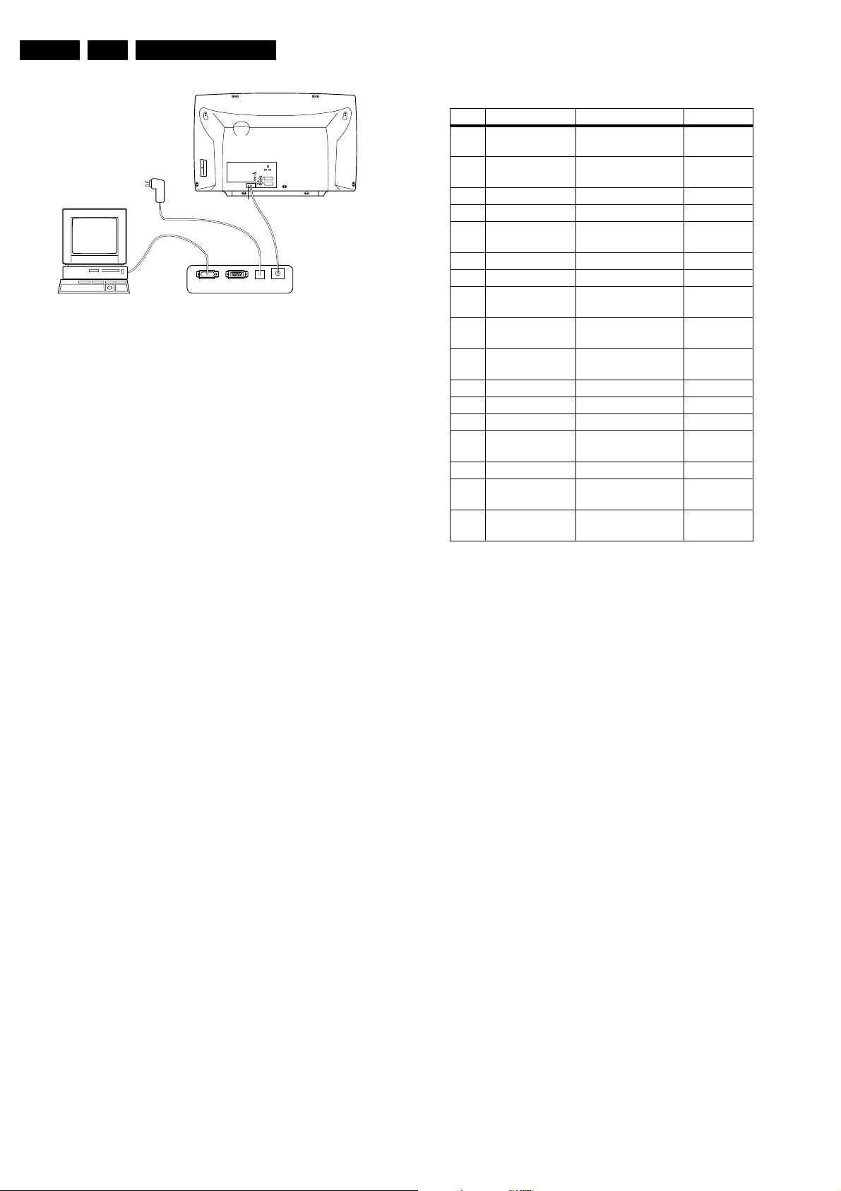
5.4.3 How to connect the ComPair Interface
1. First, install the ComPair Browser software on your PC
(read the installation instructions carefully).
2. Connect the RS232 interface cable between a free serial
(COM) port of your PC and the PC connector (marked 'PC')
of the ComPair interface.
3. Connect the AC power adapter to the supply connector
(marked with 'POWER 9V DC') on the ComPair interface.
4. Switch the ComPair interface OFF.
5. Switch the television set OFF.
6. Connect the ComPair interface cable between the
connector on the rear side of the ComPair interface
(marked with ' I
2
C ') and the ComPair connector on the
mono carrier (see “ComPair interface connection” figure).
7. Plug the AC power adapter in the AC power outlet and
switch on the interface. The green and red LEDs light up
together. The red LED extinguishes after approx. 1 second
while the green LED remains lit.
8. Start ComPair and select 'File' menu, 'Open...' select
'EM1.1A Fault finding' and click 'OK'.
9. Click on the icon to switch the communication mode 'ON'
(the red LED on the ComPair interface will light up).
10. Apply AC power to the television set with the 'POWER'
switch.
11. If the set is in STANDBY, click on 'Start up in ComPair
mode from standby' in the ComPair EM1.1A faultfinding
tree; otherwise, continue.
Page 14
EN 14 EM1.1A AA5.
EXTERNAL 2
L
R
AUDIO EXTERNAL 1
SERVICE
CONNECTOR
PC VCR I2CPower
9V DC
Figure 5-1 ComPair interface connection
The set has now started up in ComPair mode. Follow the
instructions in the faultfinding tree to diagnose the set. Note
that the OSD works, but the actual user control is disabled
5.5 Error Buffer
5.5.1 Introduction
The error code buffer contains all detected errors since the last
time the buffer was erased. The buffer is written from left to
right. When an error occurs that is not yet in the error code
buffer, it is written at the left side and all other errors shift one
position to the right.
Service Modes, Error Codes, and Fault Finding
Table 5-1 Error Codes
Error Device Description Remarks
1 FBX 3V3 protec-
tion
2 No HFB No Horizontal Fly-
4 5V protection 5V protection -
5 No HOP POR Startup failure -
6 General I2C bus
error
7 Mains Dip error HW error -
CL96532159_029.eps
190601
9 TEDE9 Tuner protection -
10 MC24C32 NVM communica-
11 MC24C32 NVM identification
12 SAA5667 Main uP, int. RAM
14 MSP3451 MSP34xx -
15 CY7C1019 SRAM test failure EM1.1A only
22 TDA9178 Histogram IC -
30 TDA9320 HIP I/O video
31 SAA4978 PICNIC -
32 TDA9330 HOP video control/
35 M62320 I/O expander HD
FBX 3V3 protection -
back
General I2C bus error
tion error
error
test failure
processing
geometry
Jack
-
-
-
-
-
-
-
-
5.5.2 How to Read the Error Buffer
Use one of the following methods:
• On screen via the SAM (only if you have a picture).
Examples:
– ERROR: 0 0 0 0 0 : No errors detected
– ERROR: 6 0 0 0 0 : Error code 6 is the last and only
detected error
– ERROR: 9 6 0 0 0 : Error code 6 was detected first and
error code 9 is the last detected (newest) error
• Via the blinking LED procedure (when you have no
picture). See 'The Blinking LED Procedure' section.
•Via ComPair.
5.5.3 How to Clear the Error Buffer
Use one of the following methods to clear the error buffer:
• Activate the 'CLEAR ERRORS' command in the SAM
menu.
• Transmit the command 'DIAGNOSE-99-OK' with ComPair.
• If the contents of the error buffer have not changed for 50
hours, the error buffer resets automatically.
5.5.4 Error Codes
If the set has non-intermittent faults, clear the error buffer
before starting repairs. This is to ensure that “old” error codes
are not present.
If possible, check the entire contents of the error buffer. In
some situations, an error code is only the result of another error
code (and not the actual cause of the problem). For example,
a fault in the protection detection circuitry can also lead to a
protection.
Explanation of error codes:
Error 0
No errors
Error 1
‘FBX 3V3 protection’
This protection is activated when the PICNIC (pos. 7709 on
diagram B3) cannot communicate via I
2
C for a certain time.
This could mean that stabilizer 7009 (B7) or 7713 (B3) on SSB
(depending on the set) is defective. When there is a short circuit
to ground behind the stabilizer, 7009 or 7713 could become
very hot. For safety reasons, the set will switch to protection
mode.
Error 2
‘No Horizontal Flyback protection’
The HOP (pos. 7301 on diagram B4 detects the absence of an
HFB pulse (pin 3 of connector 1424 on LSP, diagram A3)). A
bit will be set in the HOP. After filtering by the software, the set
will switch to protection mode.
Error 4
‘+5V protection’
When the +5V protection is active, the set is switched to
protection mode and error code 4 is placed in the error buffer.
The LED will blink 4 times (repeatedly).
A 5V failure can cause a drop in the 5V supply output, resulting
in an undefined behavior of the set. Therefore, some I
2
C
devices (Tuner and MSP) connected to the 5V supply are
constantly monitored. When none of these devices responds to
the microprocessor for a prolonged time, the microprocessor
assumes that there is a failure in the 5V supply.
By starting up (by disconnecting/reconnecting the set from the
mains) the set while short-circuiting the SDM solder pads on
the SSB, the +5V protection will be overridden, and it will be
easier to determine the cause. The +5V protection will be
activated when these I
2
C devices fail (no I2C communication):
– Main Tuner (pos. 1200 on the LSP),
– MSP3452 sound processor (pos. 7651 on the SSB).
Page 15

Service Modes, Error Codes, and Fault Finding
EN 15EM1.1A AA 5.
The following tips are useful to isolate the problem area, after
overriding the +5V protection. Determine whether:
– The MSP sound processor is loading the +5V; isolate 3650
and/or 4604 (see diagram B6).
– The main Tuner is loading the +5V source; isolate coil
5901.
Error 5
‘HOP POR error’
When the POR bit is not communicated during startup, the
processor will generate 'HOP POR not successful.'
Error 6
‘General I
2
C error’
This will occur in the following cases:
– SCL or SDA is shorted to ground.
– SCL is shorted to SDA.
– SDA or SCL connection at the microprocessor is open.
Error 7
‘Mains Dip error’ Hardware error; this error indicates
problems with the mains.
Error 9
‘TEDE9’ Tuner protection of the main tuner.
Error 10
‘NVM error’
Non Volatile Memory (EEPROM - pos. 7012) does not respond
to the microprocessor.
Error 11
‘NVM Identification error’
During the last startup, the NVM and the microprocessor did
not recognize each other (for example, one of them was
replaced, or the NVM memory has been changed/adapted or
lost), therefore the NVM was loaded with default values.
Error 12
‘Painter error’
Microprocessor (Painter - pos. 7001) internal RAM test failure.
Error 14
MSP error
Sound controller MSP34xx (pos. 7651) does not respond to the
microprocessor.
Error 22
Histogram IC error
Error 30
HIP I/O error
TDA 9321 HIP I/O video processing I
2
C communication failure.
Error 31
PICNIC error
SAA4978 PICNIC I
2
C communication failure.
Error 32
HOP error
TDA 9330 HOP video control/geometry I
2
C communication
failure (pos. 7301 on the SSB).
Error 35
I/O expander error
I/O expander IC M62320P I
2
C communication failure.
Note: Error codes 1, 2, 4, and 7 are protection codes, and in
this case supplies of some circuits will be switched off. Also, in
protection, the LED will blink the number of times equivalent to
the most recent error code.
5.6 The 'Blinking LED' Procedure
Via this procedure, you can make the contents of the error
buffer visible via the front LED. This is especially useful for fault
finding when there is no picture.
When the SDM is entered, the LED will blink the contents of the
error buffer.
Error codes > 10 are shown as follows:
– a long blink of 750ms (which is an indication of the decimal
digit),
– a pause of 1.5s,
– n short blinks (n = 1 - 9),
– when all the error codes are displayed, the sequence
finishes with a blink of 3s,
– the sequence starts again.
Example of error buffer: 12 9 6 0 0
After entering SDM:
– 1 long blink of 750ms followed by a pause of 1.5s,
– 2 short blinks followed by a pause of 3s,
– 9 short blinks followed by a pause of 3s,
– 6 short blinks followed by a pause of 3s,
– 1 long blink of 3s to finish the sequence,
– the sequence starts again.
Note: If errors 1, 2, 4 or 7 occur, the LED always gives the most
recent error, even if the set is NOT in service mode.
5.7 Protections
5.7.1 General
This chassis has only one microprocessor (Painter) which
remains active during Standby. This is because power for the
microprocessor and the memories comes from the 3V3 supply,
which is derived from the 5V Standby circuitry. Therefore, in
both Power On and Standby mode the microprocessor is
connected to this power supply.
If a fault situation is detected, an error code will be generated,
and if necessary, the set will be put in the protection mode. The
protection mode is indicated by blinking of the LED (at a
frequency of 3Hz). In some error cases, the microprocessor
does not put the set in the protection mode. The error codes of
the error buffer can be read via the service menu (SAM), the
blinking LED procedure, or via DST/ComPair.
To get a quick diagnosis, this chassis has 3 service modes
implemented:
• The Customer Service Mode (CSM).
• The Service Default Mode (SDM). Startup of the set in a
predefined way.
• The Service Alignment Mode (SAM). In this mode, items of
the set can be adjusted via a menu and with the help of test
patterns.
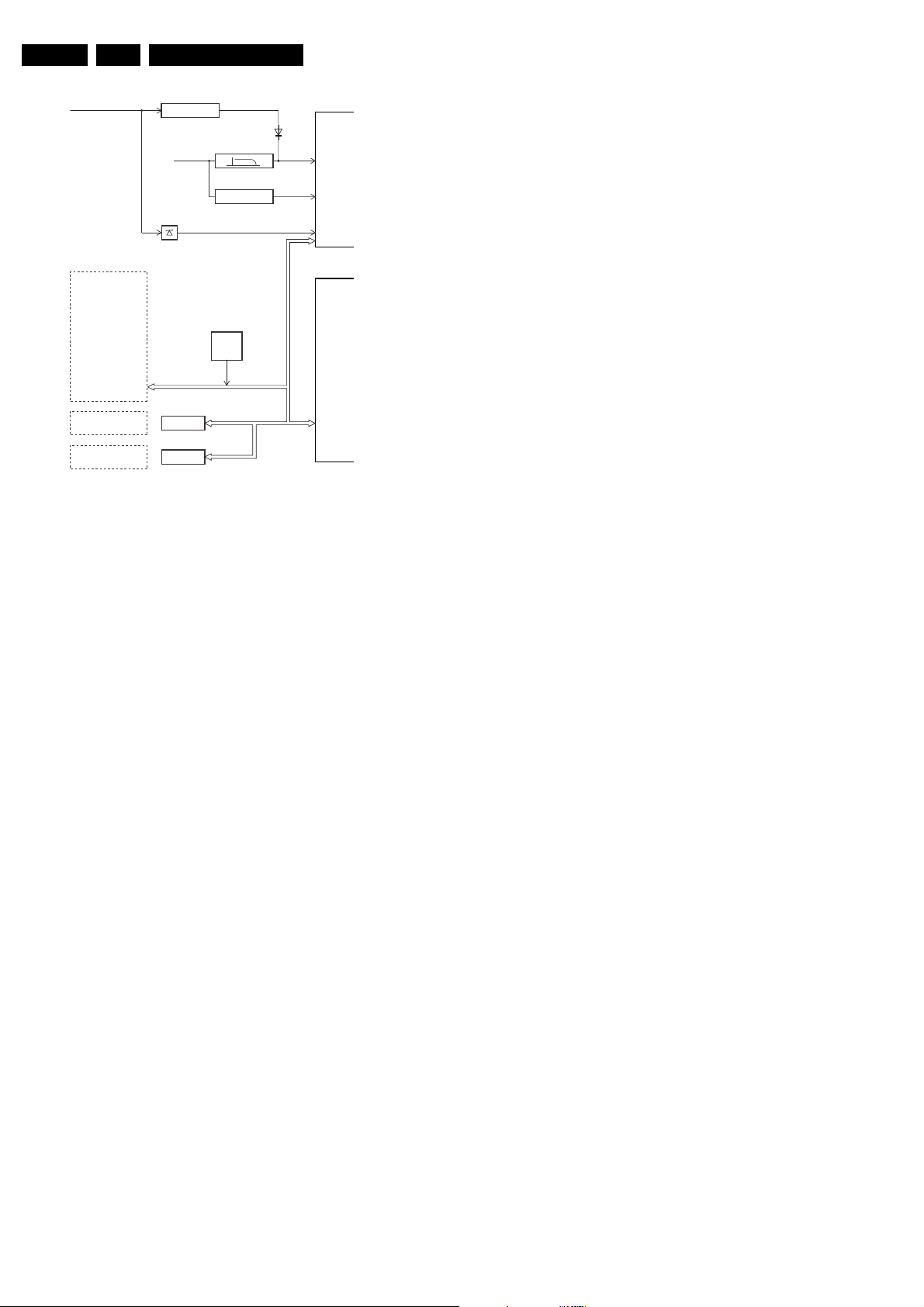
The “Protection Diagram” shows the structure of the protection
system. See diagram below.
Page 16
EN 16 EM1.1A AA5.
Service Modes, Error Codes, and Fault Finding
HFB X-RAY PROTECT
I2C SLOW BUS
HIP
HOP
PICNIC
TUNER
NVM
MSP
BOCMA DW
IO-EXPANDER DW
TUNER - DW
MULTI-PIP PROC. DW
IO-EXPANDER HD-JACK
V-CHIP
FBX
PROTECTION
TUNER
PROTECTION
X-RAY PROTECT
EHT-INFO BCL
FLASH DETECT
HFB
+5V2
PICNIC 3V3
TUNER 8V
I2C
XPR (43)
FLS (5)
NHF (13)
I2C
I2C
CL 16532043_013.eps
HOP
PAINTER
190601
Figure 5-2 Protection diagram
There are several types of protections:
2
•I
C related protections (for example, +5V supply check).
• HOP related protections (mainly for deflection items).
• Hardware errors which are not sensed by the Painter (for
example, BRIDGE_PROT)
2
I
C related protections
In normal operation, some registers of the I
will be refreshed every 200ms. During this sequence, the I
busses and the I
take place if the SDA and SCL are short-circuited to ground or
to each other. An I
2
C ICs will be checked. The I2C protection will
2
C error can also occur if the power supply
2
C controlled ICs
2
C
of the IC is missing (for example, FBX_PROT: error 1).
HOP related protections
Every 200ms, the status register of the HOP is read by the
Painter via I
2
C. If a protection signal is detected on one of the
inputs of the HOP, the relevant error bit in the HOP register is
set to “high.” If the error bit is still “high” after 1s, the Painter will
store the error code in the error buffer (NVM) and, depending
on the relevance of the error bit, the set may or may not go into
protection mode.
• HFB: Horizontal Flyback. If the horizontal flyback is not
present, then this is detected via the HOP (HFB_XRAY_PROT). One status bit is set to “high.” The error code
is stored in the error buffer and the set will go into the
protection mode.
• Flash detection. From the EHT info, via D6303 and T7303,
a flash will stop the H-drive and line output stage
immediately. The FLS bit in the status register of the HOP
is set to “high.” As the duration of a flash is very short, the
FLS bit will be reset to “low” again after the flash refresh,
and the set will be started again via a slow start.
Hardware related protections
Due to the architecture (with “hot” deflection) there are two
protections that are “unknown” to the microprocessor, namely
the 'BRIDGE_PROT' (coming from the line stage) and the
'DEFL_PROT' protection (coming from the frame deflection
stage).
If one of these protections is triggered, the set is switched to
“Standby” mode. The Painter will now try to restart the set. If
this does not succeed after 5 times (after 30 - 60 seconds), the
Painter will generate error 2 (this error can have several
causes, such as repeating flashes, BRIDGE_PROT/Non VFB
leading to DEFL_PROT, or a serious AC power dip). The red
LED will start blinking.
5.8 General tips and repair tips
5.8.1 General
Notice that a very large part of the set (Large Signal Panel) is
“hot,” meaning the primary part of the Standby supply, the
whole Main supply (except for the secondary Audio supply),
and the complete deflection circuit are "hot."
Note: The deflection-coil is hot.
This set is not equipped with an IR transmitting LED. Instead,
a Service (ComPair) connector is implemented at the rear of
the set, which is directly accessible (it is not necessary to
remove the back cover to access the connector).
In addition to this, there is a blinking LED procedure to show the
contents of the error buffer.
The relay you hear during switching the set “on” (via the power
switch) is from the degaussing circuitry. So it is not used for
switching the supply as in the MG chassis.
When there is a menu on the screen, it is not possible to enter
a service mode. Be sure there is no menu on the screen when
attempting to enter a service mode.
5.8.2 Main Power Supply
The simplest way to repair the main supply is to check (and
replace, if necessary) the gray marked components on the
Main Supply.
Do not try to perform measurements on the side of the SSB
connected to the "hot" heatsink. This is dangerous. Most
relevant service test points are connected to the Tuner side
and are pointed out by service printing. Where the circuitry was
too crowded to place this service printing, it has been explained
on the Test Point Overviews in this manual. It is also possible
to use the SSB extension panel (part number: 9965 000
05769), so that all test points are easily accessible.
5.8.3 Standby Power Supply
The simplest way to repair the standby supply is to check (and
replace, if necessary) the gray marked components on the
Standby Supply.
5.8.4 Horizontal Deflection
The simplest way to repair the horizontal deflection is to check
(and replace, if necessary) the gray marked components on the
Horizontal Line Deflection circuitry.
5.8.5 Vertical Deflection
Caution: When you suspect the Vertical Deflection circuitry,
please be careful. Since there is a DC voltage on the vertical
deflection, the beam current can damage the CRT neck,
leading to a defective CRT.
The best thing to do is:
1. Interrupt pin 2 of connector 1424 on the CRT panel
(diagram F), in order to remove the 'filament' voltage from
the tube (there is no beam current, so there is no chance of
destroying the CRT).
2. Measure the functionality of the Frame stage with a
multimeter or with an oscilloscope.
3. After you have found the cause, exchange the defective
component (for example, TDA8177), and resolder the
interrupted pin 2.
Page 17
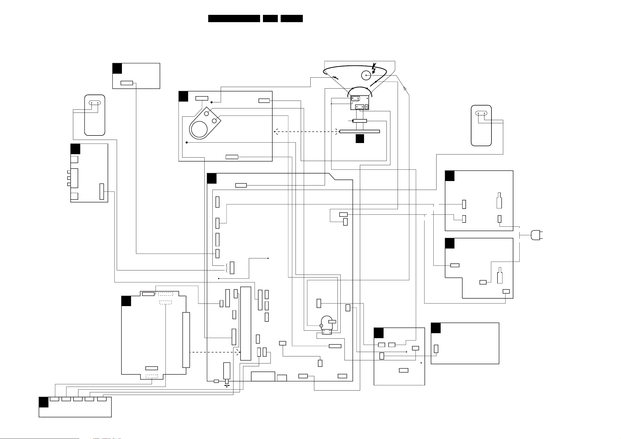
Block Diagrams, Testpoint Overviews, and Waveforms
6. Block Diagrams, Testpoint Overviews, and Waveforms
Wiring Diagram
17EM1.1A AA 6.
CVBS (YELLOW)
LEFT (WHITE)
RIGHT (RED)
HEADPHONE
SVHS
O
BLUE
BLUE
RIGHT
SPEAKER
SIDE
I/O PANEL
1936
11P
TOP CONTROL
P
PANEL
0215
3P
(COMPONENT VIEW)
1940
F
F
11X
1435
CRT
PANEL
CRT
SOCKET
1434
A
8335
1483
3P
BLACK
RED
1424
7X
LSP(LARGE SIGNAL PANEL)
1620
3P
1146
N.C.
5P
1947
5P
PV2 MODEL
1946
9P
1945
3P
1735
2P
2P
4P
AQUADAG
1505
1502
DEGAUSSING COIL
CRT
BROWN
BLUE
SCAVEM
COIL
CRT PANEL
2P
2P
FRAME
ROTATION
COIL
1010
2P
1009
3P
F
1008
2P
8502
EHT
CRT
A (LOT)
BROWN
BROWN
LEFT
SPEAKER
MAINS SWITCH PANEL
J
(PV2 MODEL)
0247
OR
OR
OR
OR
J
5P2P
0212
MAINS SWITCH PANEL
(FL9 MODEL)
0247
5P
0211
MAINS
SWITCH
2P
OR
OR
MAINS
CORD
6P
7P
1680
1304
N
JACK HD PANEL
1934
0201
1205
1951
3X
SSB
B
5P
4P
6P
1933
1104
1681
1303
5P
1304
7P
N.C.
10P
3P
10P
1937
1955
N.C.
1940
TUNER
SPLITTER
5P
3P
11P
N.C.
1682
6P
1680
1000
80P
8937
8940
1943
3P
compair
interface
1948
80P
SSB
PANEL
1935
1934
1936
5P
CINCH
N.C.
6P
11P
12x
1933
N.C.
3P3P3P
N.C.
1953
N.C.
1499
2P
4P
1625
SVHS
3P
8424
1417
2P
LOT
1424
1498
2P
1P
1419
HORIZONTAL
I
DAF PANEL
1417 1418
2P
7P
1492
N.C.
3P
2P
2P
1419
1492
3P
1491
N.C.
1497
1P
8418 (30")8417
1693
N.C.
DC SHIFT
G
(IF APPLICABLE)
0317
2P
2P
-CL 36532061_001.eps
MAINS
0202
2P
030903
SWITCH
Page 18
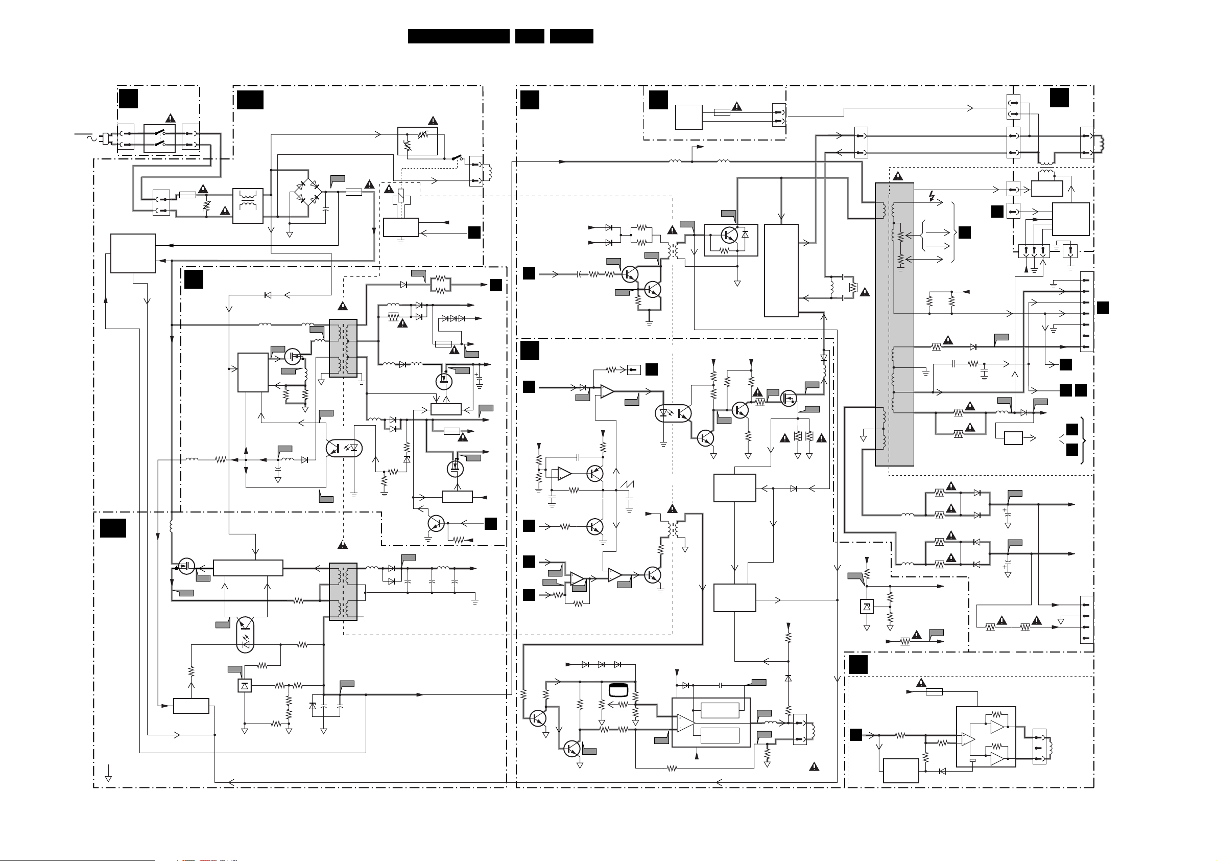
Block Diagrams, Testpoint Overviews, and Waveforms
18EM1.1A AA 6.
Block Diagram LSP Supply and Deflection
SUPPLY DEFLECTION
J
0201
OR
0211
2
1
7505, 7506, 7503
QUICK
SWITCH
MAIN SUPPLY
+VBATT
A1B
MAINS
SUPPLY
HOT GROUND
FRONT
INTERFACE
0231
OR
1051
2
1
1505
OFF
SUP-ENABLE
+375V
-20V
-20V
SUP-ENABLE
2
1
0202
OR
0212
2
4
1
3
1501
T5AH
A2
5517
7504
STP5NB60FP
D
G
S
A3
3531
7529
ACTIVATING
CIRCUIT
A1A
5502
5511
5503
5516
5504
3509
V
STAND-BY SUPPLY
A2
TCET1103
31205106
7502
7530
A4
7507
7506
TL431CZP
MAINS
FILTER
STARTUP
7100
7101
7105
7120
CONTROL
CIRCUIT
-20V
CONTROL
CIRCUIT
324
A5
1
2
SUP-ENABLE
6109
7102
STP3NB60
-20V
MAIN SUPPLY
1
3506
3
MAIN SUPPLY
6525
GBU4J
V-START
A11
3108 3118
3530
3510
3526
GND-SUPGND-FB
4
-
GND-STB
V-START
51095101
D
G
S
A12
5113
GND-STB
A13
6103
5102
2102
GND-STB
3514
3520
VBATT
ADJUSTMENT
3507
6514
3527
2
+
3
A10
5104
GND-STB
GND-FB
A1
1
+
2516
3
2
1
A15
7103 OR
5
4
A16
5506 OR
5
4
3
1
HOT
2523 2515
1503
F2.5AH FOR
AP (PAL)
F4AH FOR
AP (NTSE)
5100
7104
5512
COLD
A6
+375V
65
7
8
10
1
2
6
7
9
10
3550
21
RP
0+
RS
3
1
1550
4
7501
7528
ACTIVATING
CIRCUIT
A17
6110
6113
5112
3161
5111
5103
3114
5507
N.C.
6107
6111
3124
6535
6539
6130
3113
6122
6148
5130
STP16NE06
STP16NE06
A7
+
2512
+VBATT
8+
DEGAUSSING
3115
3116
6117
1148
1A25
+8V6-SWITCH
7131
D
G
CONTROL
1147
1A6
+5V-SWITCH
7141
D
CONTROL
7132
5514
+
2546
2
+5.2V_MP
PAINTER
VTUN
6119
6118
A20
S
7133
7130
S
G
7140
3173
+
2542
1502
3
2
1
HOT
COLD
B7
+11V_STBY
+11V_ROT
+11V
A18
+5.2V_MP
A21
STANDBY
+11V_STBY
+28V
GND-AUD
A8
+8V6
2126
A19
+5.2V
+5V
+8V6
B7
PAINTER
COLD
HOT
DEG.
COIL
LINE DEFLECTION
A3
+VBATT
HOT
COLD
LINEDRIVE 1
B4
HOP
FRAME DEFLECTION
A4
E/W DRIVE
EW-DRIVE 1
B4
HOP
CURRENT
+8Vb
SOURCE
3455
3456
A3
HOP
FRAMEDRIVE +
7440-B
5
6
3419
2404
HFB_X-RAY-PROT
3459
B4
A34
+8V-S
A33
3658
3640
3
2
3631
7612
HOP
B4
HOP
FRAMEDRIVE -
COLD
HOT
3660
7611
+11D
+5.2V
+
6456
5
6
A37
+8Vb
3457
2403
7
7441
7455
7440-A
1
A35
3657
6627 6626 6625
3642
3632
A39
6408
6407
341434062492
3654
7450-B
3
2
3415
3416
A22
7409
A23
3404
1693
7
A38
FRAME DEFLECTION
2457
+8V6
7614
7450-A
1
A36
TV
3638
3643
3630
3634
DC-SHIFT (OPTIONAL)
G
DC-
SHIFT
CIRCUIT
5400
A25
5410
94
A24
61
7408
COLD HOT
E/W - DRIVE
TO 1693
I
DAF
7482
1
2
7487
5621
6
1
5
10
3641
+13V-LOT
6620
7620
TDA8177
7
OP. AMP
1
A40
-15V-LOT
3623
1430
400 mA
+141V
5401
7421
BU2520DX
SUP-ENABLE
+8V-S +141V
3492
3484
5
A45
4
7442, 7654
7653
PROTECTION
7641
7443
7652
PROTECTION
2622
62
FLYBACK
GENERATOR
THERMAL
PROTECTION
4
A26
3493
7486
EW
CIRCUIT
ARC-PROT
CIRCUIT
1419
TO
A4
E/W
DRIVE
A28
2443
5461
A30
1492
7445
1
2
1417
1
2
1497
1
1693
1
+11D
A31
2462
A32
2464
6460
5
8
FILAMENT
34993498
HOR. DAF
CIRCUIT
+11D
312
HFB_X-RAY-PROT.
HFB_X-RAY-PROT.
A29
1620
1
2
3
CL 36532061_002.eps
0317
1
2
LINE
OUTPUT
CIRCUIT
+
EW
CORR.
7480
3488
STP3NB60
A46
G
3481
3479
3483
SUP-ENABLE
-15V_LOT
A42
3
3647
A43
5
5620
A44
3620
6491
3627
6619
1625
5421
6480
5467
A47
D
S
A48
3480
EW
1
2
VERT.
DEFL.
COIL
2430
2431
1417
1
2
5430
LOT
5
1
3431
3
4
6
HOT COLD
5463
+13V-LOT
A50
1
7613
TL431
2
ROTATING CIRCUITRY
A5
TILT
B4
HOP
5465
3635
3636
3
3637
3449
+11D +8Vb
+11V_ROT
3686
7681
7682
SWITCH OFF
CIRCUIT
IN STAND-BY
EHT
VG2
10
8
11
9
12
FOCUS A
FOCUS B
3400
3463
3462
3465
3464
A49
1601
125mA
3685
DYNAMIC FOCUS
TO
F
CRT
3450 3451
6400
3437
2442
FILAMENT
3460
3461
+8V-S
7680
TDA7052
2
3
3684
6080
+11D
EHT-INFO
6463
6462
6465
6464
1
+Vp
6
I
5800
VER. DAF
CIRCUIT
(OPTIONAL)
FILA-
MENT
EHT-INFO
HOP
+11D
PORPOR
+13V - LOT
-15V - LOT
+13V LOT
-12V8
ROTATION
DEFLECTION
COIL
DAF
HOT
COLD
1491
1
PULSES
200V
B4
3X
A4 B4
B4
HOP
A6
AUDIO
COLD
HOT
HOT
COLD
020903
1418
1424
1495
1
2
1
2
3
4
5
6
7
1
2
3
4
LINE
DEFLECTION
COIL
TO
1224
F
CRT
TO
PANEL
ON
CRT
NECK
(optional)
Page 19
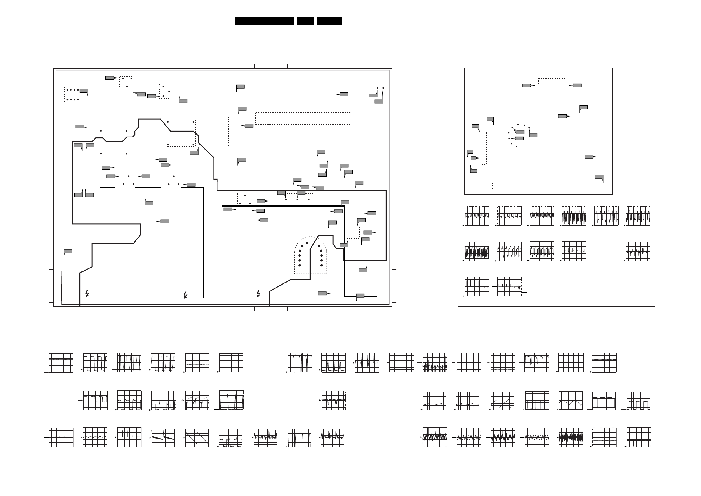
Block Diagrams, Testpoint Overviews, and Waveforms
Testpoint Overview LSP and CRT
LSP COPPER TRACK SIDE
2 3 4 5 6 7 8 9 10
S
A20
D
STANDBY
SUPPLY
TRAFO
5100
A10
A11
G
7131
+8V6
106
15
D
7102
STANDBY
SUPPLY
G
A19
A12
S
A
B
C
D
E
F
G
1
1
A18
8
7680
ROTATION
A17
A15 A16
A13
A14
A71
1 2 3 4 5 6 7 8 9 10
G
A21
D
7141
S
+5V
SUPPLY
TRAFO
A4
A5
D
G
7504
MAIN
A2
SUPPLY
A1
ATTENTION:
LIVE PARTS
A7
MAINS
5506
S
19EM1.1A AA 6.
A1
E4
A58
A2
D3
A3
D4
A4
A5
A6
A7
A10
A11
A12
A13
A14
A15
A16
A17
A18
A19
A20
A21
A22
A23
A24
A25
A26
A28
A29
A30
A31
A32
A33
A34
A35
A36
A37
A38
A39
A40
A41
A42
A43
A44
A45
A46
A47
A48
A49
A50
A56
A57
C4
C4
C5
A4
C2
C2
D3
D1
D1
C1
C1
B1
A1
A3
A2
A3
D8
D8
D8
D8
D7
G9
G10
G10
E9
E9
C8
D9
C9
D10
D9
C9
D10
E10
E10
E10
F10
E10
D7
E6
E7
E7
C9
D9
C6
B6
A69
A70
45
A
B
A59
A56
14
610
7701
AUDIO
12
A58
80
SSB
11
TUNER
A68
1
AMPL
51
A6
A3
A46
1
A33
A57
A23
D
E/W
A45
S
A48
A47
G
7480
A22
A26A25
7421
LINE
58
49
3
2
1
LOT 5430
A35
A34
A24
ECB
6
A31
A32
7620
FRAME
A38
A39
A41
A37
A36
1
7
A42
A40
A44
A43
10
11
12
A29
C
D
E
F
G
A28
A30
COLDHOTCOLD HOT
A59
A68
A69
A70
C6
B5
A9
A10
A10
CRT PANEL (COPPER TRACK SIDE)
1424
7
F15
F13
F5
9
F6
F1
1
F3
F1
1 V / div DC
20µs / div
F7
20 V / div DC
20µs / div
F13
1 V / div DC
20µs / div
F4
7307
R
F9
B
F8
1435
11 1
F2
1 V / div DC
20µs / div
F8
20 V / div DC
20µs / div
SC3
20 V / div AC
20µs / div
G
F7
F3
1 V / div DC
20µs / div
F9
20 V / div DC
20µs / div
Measured across
6, 10, 5300
1
F10
F4
20 V / div DC
20µs / div
F10
50mV / div DC
20µs / div
F12
F14
SC3
F5
20 V / div DC
20µs / div
F1
E4
F2
D3
F3
D4
F4
C4
F5
C4
F6
C5
F7
A4
F10
C2
F12
D3
F13
D1
14
D1
A15
C1
A16
C1
A17
B1
A18
A1
A19
A3
A20
A2
A21
A3
A22
D8
A23
D8
A24
D8
F6
20 V / div DC
20µs / div
F12
1 V / div DC
20µs / div
A1
PM3394B
50V / div DC
2us / div
A21: 5V1 DC
A40
PM3394B
2 V / div AC
5ms / div
A2
50V / div DC
5us / div
A22
1V / div DC
10us / div
A41
2 V / div AC
5ms / div
PM3394B
PM3394B
PM3394B
A3
PM3394B
50V / div DC
5us / div
A23
PM3394B
200mV / div DC
10us / div
A42
PM3394B
10 V / div AC
5ms / div
A4
50V / div DC
5us / div
A24
5V / div DC
10us / div
A43
10V / div DC
2ms / div
PM3394B
PM3394B
A5
PM3394B
5V / div DC
10us / div
A25
PM3394B PM3394B
1V/div DC
10us/div
A44
PM3394B
200mV / div DC
2ms / div
A6 A7: 33V DC
PM3394B
20V / div DC
10us / div
A28: 206 V DCA26: A29: 11V4 DC
200 V / div DC
10µs / div
A45
1V / div DC
10µs / div
PM3394B
A46
500mV / div DC
10µs / div
PM3394B
A10
50V / div DC
5us / div
A47
50V / div DC
10µs / div
PM3394B
PM3394B
A11
PM3394B
5V / div DC
5us / div
A30
PM3394B
50 V / div DC
10µs / div
A48
PM3394B
500mV / div DC
10µs / div
A12
PM3394B
2V / div DC
5us / div
A31: 13V DC A32: 15V DC
A13
5V / div DC
10us / div
PM3394B
A14
PM3394B PM3394B PM3394B
200mV / div DC
10us / div
A33
PM3394B
500mV / div DC
2ms / div
A56
PM3394B
20mV / div AC
1ms / div
A15
500mV / div DC
5ms / div
A34
PM3394B
500mV / div DC
2ms / div
A57
PM3394B PM3394B PM3394B PM3394B
500mV / div AC
1ms / div
A16
5V / div DC
5ms / div
A35
PM3394B
500mV / div DC
2ms / div
A58
20mV / div AC
200µs / div
A17
PM3394B
20V / div DC
5us / div
A36
PM3394B
200mV / div DC
10us / div
A59
500mV / div AC
1ms / div
A18
PM3394B
5V / div DC
5us / div
A37
PM3394B
500mV / div DC
2ms / div
A68
500mV / div AC
20µs / div
A19
PM3394B
1V / div DC
5us / div
A38
PM3394B
200mV / div DC
10us / div
A69
PM3394B
2 V / div DC
100ms / div
A20: 8V DC
A39
PM3394B
2V / div DC
10us / div
A70
PM3394B
2 V / div DC
100ms / div
CL 36532058_007.eps
030903
Page 20
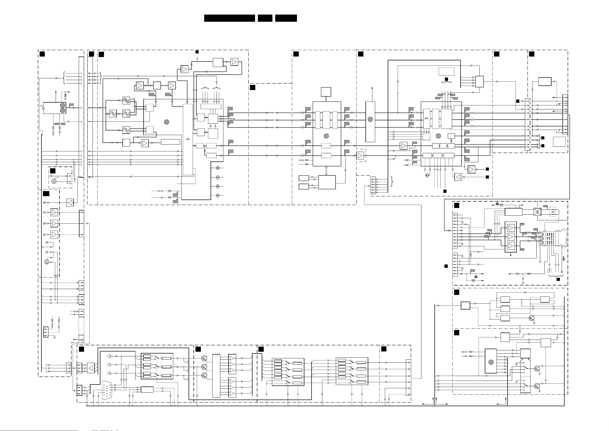
Block Diagrams, Testpoint Overviews, and Waveforms
Block Diagram Video
20EM1.1A AA 6.
VIDEO
TUNER, I/O,
A8
SIMM-CONN.
1200
TUNER
F
B
A
D
C
E
154
I/O
A11
MONITOR
OUT
7992
7993
U/B
7994
7995
Y/G
7990
7991
V/R
AV1
CVBS
B
B
AV2
CVBS
32
154
SVHS-AV2
C
D
B
E
A
1943
1
2
3
F
R-SC1
B-SC1
G-SC1
FBL-SC1
+5VT
6200
BZM55-C33
9
7.3
ERR
9
11
ERR
13
15
4
AGC
A69 A70
3201
3200
SDA
SDL
CVBS-SC1-AV1-IN
Y-CVBS-SC2
Y-CVBS-FRONT-IN
C-FRONT-IN
C-SC2-SVHS-IN
SIDE I/O
O
Y-CVBS-FRONT
32
C-FRONT-IN
SVHS
7902
CVBS
SC1-B-IN-U-IN
SC1-G-IN-Y-IN
SC1-R-IN-V-IN
CVBS-SC1-AV1-IN
C-FRONT-IN
Y-CVBS-FRONT-IN
CVBS-SC1-AV1-IN
C-SC2-SVHS-IN
Y-CVBS-SC2-AV2-IN
SDA-S
SCL-S
32623261
COMPAIR CONN.
(SERVICE)
SC1-R-IN-V-IN
SC1-G-IN-Y-IN
SC1-B-IN-U-IN
7320
EF
26 29 28
VIDEO
SWITCH
+
CONTROL
12
1
1
2
2
3
3
B7
CVBS TXT
COMB-C-OUT
Y
PROC.
C
PROC.
SYNC
SEPAR.
N4
Y-G
Y
C
7451
7452
7453
N.C.
41 42 43
MATRIX
12
RGB
MATRIX
Y
Y/U/V
SWITCH
U
DECODER
PAL
NTSC
SECAM
V-SYNC
PROC.
H-SYNC
PROC.
54
55
56
57
7307
TDA9181
COMB
FILTER
RGBRGB
36
37 38
UV
Y
U
V
V
1315
4.4342
1318
3.582056
1318
3.575611
1318
3.579545 MHz
-MATRIX-
YPBPR
YUV
MATRIX
7412
14
16
COMB-Y-CVBS-OUT
V6
Y50
V7
49
50
U50
51
V8
V50
F14
61
VA50
L8
60
HA50
PAL BG
PAL N
PAL M
NTSC M
7400
5
6
10
9
12
13
7450
5
6
10
9
12
13
3747
Y100
3748
U100
3749
V100
7704
5
IO-2
1110
VIDEO CONTROL+
B4
GEOMETRY
+8VS
7302
20
TDA9178
TOPIC
6
(OPTIONAL)
ERR
8
22
9
1304
1
2
3
4
5
6
R-OUT
12
3-STATE
G-OUT
11
3-STATE
B-OUT
10
3-STATE
13
3-STATE
16
DECODING
I0-3
91312
19
17
16
R-2FH
G-2FH
B-2FH
FBL-2FH
HD100
VD
FBL
VD
HD100
2x
INPUTS / OUTPUTS
N2
R-OUT
G-OUT
B-OUT
FBL
H-OUT
V-OUT
2429
FBL-2FH
R-2FH
G-2FH
B-2FH
SDA
SCL
SIM CONN.
B1
YLTP
FROM
BLOCKDIAGRAM
CONTROL
B7
CONTROL
R-TXT
G-TXT
B-TXT
FBL-TXT
V24 V26
V25
7301
TDA9330H
V19
2323
Y100
U100
V100
7304
28
V20
2322
V21
2321
F17
L12
V23
3321
V22
3320
Y/U/V
RGB
27
MATRIX
26
YUV
33
30
RGB
YUV
MATRIX
PH1-1
1301
12M
V-DRIVE
PROC.
2120
SANDCASTLE
PH1-2
91413
ERR
32
HFB-X-RAY-PROT
31
32
23
24
11
10
35 36 37 38
RGB
INSERTION
OUTPUT
AMPL.
CATHODE
CALIBR.
DRIVE
RAMP
FRAME
GEN
STARISTOP
H-DRIVE
29
22
DYN-PHASE-COR
POR
B5
V27
R
G
B
E/W
5
7303
F
1940
1
2
3
4
5
6
7
8
9
10
11
1424
1
2
FROM
3
1424
OF
4
A3
5
(LINE
6
DEFL.)
7
200V
N3
Y-G
14
2
N1
SDA
1304
1
2
14.2.3
V
3
V-770
17
H-770-3
15
H
2
H-770-2
16
15.16.17
3
4
5
6
SCL
7305
7306
R-2FH
G-2FH
B-2FH
V28
V29
V30
F20
F18
FRAMEDRIVE +
F19
L13
7310, 7311
+
3340
R-CRT
3341
G-CRT
3342
B-CRT
E/W DRIVE
FRAMEDRIVE -
LINEDRIVE
VSYNC
EHT-INFO
FBL-2FH
43
40
41
42
44
3
2
1
8
CRT/SCAVEM PANEL
N.C.
Y-SCAVEM
+8V
R-CRT
G-CRT
B-CRT
3417
F15
N.C.
3341
SYNC SLICER
7700
LM1881M
1
SYNC
PROC
3
CONTROL
3132
3130
B7
B4
B7
+8V
F1
F2
F3
CUTOFF
HFB_X-RAY_PROT
FILAMENT
EHT-INFO
+200V
+200V (6-7307)
7106
M62320
3
2
I/O
EXPANDER
ERR
35
Y-SCAVEM
3300
7300 : 7340
SCAVEM
PROC.
7307
TDA6108JF
37
28
1
5
6
(1)
+180V
+8V
7750-A
3
6
O.S.
4
7750-B
13
10
O.S.
11
3
6
O.S.
5
7751-A
7160
7109, 9110
PULS
FORMER
7
IO-4
9
IO-5
6
IO-3
4
IO-1
9
8
5
IO-2
11
10
IO-6
5
1112IO-7
6
IO-8
4
8.9
4.5.6
3334
B4
9
10
12
14
15
11
7102
74HC4052D
9
6
1
5
2
4
SIM CONN.
A8
1000 1205
HFB-X-RAY-PROT
32
33
41
25
24
23
21
31
26
29
28
+200V
5300
F6
F9
3352
R
F5
F8
3351
LOGIC
6
F7
3350
11
3349
2318
12
11
7713
MR
7108
3
7105
13
G
B
F4
CL 36532061_008.eps
6402
6901
PROTECTION
CIRCUIT
EHT-INFO
Y-SCAVEM
R-CRT
G-CRT
B-CRT
CUTOFF
TO
A3
TO
A4
SC3
8
7751-B
O.S.
7166
74HC4024
TIMER
CIRCUIT
+11V5
LINE
DEFL.
FRAME
DEFL.
VG1
CP
+8V
1483
1
2
3
VG2
1434
SIN
FROM
LOT
9
10
NO-FBL YPbPr
NO-FBL-RGB
020903
SEE
BLOCK-
DIAGRAM
DEFLECTION
SCAVEM
COIL
FG-A
FG-B
EHT
A3
LINE
DEFL.
H-770-3
H-770-2
V-770
NO-FBL
V-OUT
H-OUT
1940
1
2
3
4
5
6
7
8
9
10
11
HOT
COLD
CRT
15
16
7
17
10
13
12
FEATUREBOX
B3
EF
B6
4609
4608
4607
VA50
HA50
CONTROL
N1
7107
7
RA
8
BA
14
GA
7
RN
8
BN
14
GN
TDA8601T
2
RA
CLAMP
6
RN
CLAMP
3
GA
CLAMP
7
GN
CLAMP
4
BA
CLAMP
8
BN
CLAMP
15
14
Y-PIP-MAIN-IN
U-PIP-MAIN-IN
V-PIP-MAIN-IN
VA50
HA50
SDA-F
SCL-F
3-STATE
3-STATE
3-STATE
3-STATE
5
IO-1
8714654
3755
3757
3759
3733
3728
7714
FIELD
MEMORY
7715
FIELD
MEMORY
16
DECODING
I0-3
9
3705
3703
12
11
10
13
7716
PICNIC
EEPROM
7709
SAA4978H
7708
SAA4990H
41
7101
TDA8601T
2
6
3
7
4
8
15
14
Y
U
V
CLAMP
CLAMP
CLAMP
CLAMP
CLAMP
CLAMP
V14
12
V16
14
V15
15
S4
19
VD100
S3
18
HD100
V11
23
V12
3X
SIGNAL
25
ADC
V13
S7
S6
PROC.3XDAC
26
PICNIC HOP
ERR
31
V-SYNC
29
PROC.
H-SYNC
28
PROC.
5
4
PROZONIC
PR-R
1
R-MATRIX
Y-G
2
G-MATRIX
PB-B
3
B-MATRIX
NO-FBL-RGB
B1
1205 1000
3
1
2
4
VTUN
A68
13
IF
15
10
6
63
64
7
1936
2
9
4
1933
1
2
3
1953
1
2
N.C.
3
1935
1
3
N.C.
5
1937
SDA-5
1
SCL-5
2
N.C.
8
+8V
INPUTS/
N2
OUTPUTS
1934 7990 : 79951934
2
2
3
3
4
4
1933
1
2
3
IF, I/O,
B2
VIDEOPROC.
3
1
2
4
SAW FILTER
SAW FILTER
13
15
10
6
63
64
7
9
Pr-IN
1
Pb-IN
2
3
Y-IN
1990
1
2
13
14
3
H
V
32
2(2x)1
1410
SAW FILTER
5403
1408
40,4
1
2
3
R-IN
G-IN
B-IN
SAW FILTER
AUDIO
1409
1411
SOUND
BAND
PASS
TUNER AGC
H
1
3
2
1
SC1-G-IN
7411
VIF2
VIF1
SIF2
-Y-IN
EF
2
3
62
6364SIF1
7410
7901
TDA8601T
2
6
3
7
4
8
7904 : 7909
DETECTION
7323
TDA9320H
CLAMP
CLAMP
CLAMP
CLAMP
CLAMP
CLAMP
SIGNAL
1406
SOUND
FILTER
I6
10 14
PLL
DEM
QSS
MIXER
AM
DEMO
CVBS-SC1-AV1-IN
Y-CVBS-SC2-AV2-IN
Y-CVBS-FRONT-IN
C-FRONT-IN
C-SC2-SVHS-IN
CVBS-SC2-MON-OUT
SDA-F
SCL-F
5
V2
HIP
ERR
30
QSS-AM
5
QSS-AM
TO BLOCK DIAGRAM
3-STATE
3-STATE
3-STATE
7322
EF
AUDIO
16
20
23
24
21
34
32
N.C.
3377
47
V9
3376
46
V10
- HIGH DEFINITION INTERFACE - -
PR-R
12
YG
11
10
PB-B
IO-7
IO-6
IO-8
Page 21

Block Diagrams, Testpoint Overviews, and Waveforms
Testpoint Overview SSB
SSB
21EM1.1A AA 6.
TUNER SIDE
S3
64 41
65 40
PROZONIC
80 25
7708
124
64 49
1
48
MSP
7651
16
17 32
33
S4
PICNIC
EPROM
7716
1701
1
7012
C3
7005
1
76100
C7
751
51
C11
1001
C5
C4
S5
V12
S6
V15 V16S8
V13
S7
V14
25
C6
PAINTER
7001
26 50
C9
LOT SIDE
V13
V14
V15
V17
V18
S3
S5
S8
26
12
14
4
5
18
25
34
160
121
1 120
PICNIC
7709
40 81
8041
40 21
120
401
FM
7714
2120
FM
7715
C8
C10
V24
V26
V27
V28
V30
1
V19
HOP
V20
7301
V6
V21
11
V7
22
12
L8
V8
F14
1408
I6
V1
V2
64 62 60
1
10
12
14
19
20 32
F14
HIP
7323
L8
51
33
51
50
49
47
46
V8
V7
V6
V9
V10
C3
500mV/div DC
10µs/div
C4
200mV/div DC
10µs/div
C4 HSYNC
V22
V23
80 41 40 1
C11
200mV/div DC
250ns/div
F03
200mV / div AC
100ns / div
F14
L13
1V/div DC
10µs/div
S03
1V/div DC
10µs/div
S04
S6 H-A
2V / div AC
10µs / div
S7 V-A
1V / div AC
5ms / div
S8
V7
500mV/div DC
20µs/div
V8
500mV/div DC
20µs/div
V13 V-IN
V16
500mV/div DC
5µs/div
V19
1V/div DC
10µs/div
V20
V22 SCL
1V / div DC
0.2ms / div
V23 SDA
1V / div DC
0.2ms / div
V28
V30
1V/div DC
10µs/div
F14
2V/div DC
10ms/div
I6 VIF-Out
0.5V / div AC
10µs / div
L8
1404180
S5 Y-IN
0.2V / div AC
10µs / div
S8
1V/div DC
250ns/div
V1
PM3394B
V6
500mV/div DC
20µs/div
V7
500mV/div DC
20µs/div
V8
V10 SCL
1V / div DC
0.2ms / div
V13 V-IN
0.2V / div AC
10µs / div
V14
V17 SCL
1V / div DC
0.2ms / div
V18
0,5V / div DC
10µs / div
1V / div DC
20µs / div
C5 VSYNC
1V / div DC
10ms / div
2V/div DC
10ms/div
L12
1V/div DC
50µs/div
1V/div DC
5ms/div
S5 Y-IN
0.2V / div AC
10µs / div
1V/div DC
250ns/div
V6
500mV/div DC
20µs/div
0.2V / div AC
10µs / div
V14
500mV/div DC
5µs/div
1V/dic DC
10µs/div
V21
1V/div DC
10µs/div
1V/div DC
10µs/div
V29
1V/div DC
10µs/div
1V/div DC
20µs/div
S3
1V/div DC
10µs/div
1V / div DC
10us / div
V2 CVBS_INT
0.5V / div AC
10µs / div
500mV/div DC
20µs/div
V9 SDA
1V / div DC
0.2ms / div
500mV/div DC
5µs/div
V15
500mV/div DC
5µs/div
CL 36532061_007. eps
030903
Page 22
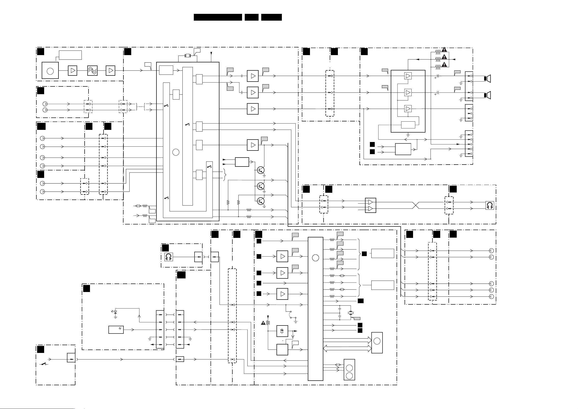
Block Diagrams, Testpoint Overviews, and Waveforms
Block Diagram Audio
22EM1.1A AA 6.
AUDIO
IF
B2
7323
TDA9320H
I/O HD
N2
AV3
R
AV3
L
I/O
A11
AV1
L
R
AV2
L
R
SIDE I/O
O
L
R
HOP
ERR
30
SND2_R_IN
SND1_L_IN
BLOCK DIAGRAM
VIDEO
7411 74101410
10
L_SC1_AV1_IN
R_SC1_AV1_IN
L_SC2_AV2_IN
R_SC2_AV2_IN
L_FRONT_IN
R_FRONT_IN
SIMM
CONN.
1680
1
3
B6
SEE
1680
0240
1
3
A8
1936
6
8
B1
10001205
52
60
53
58
65
66
SND_R_IN
SND_L_IN L
AUDIO DEMODULATOR
7651
MSP34XXG
B65
QSS-AM
R
SDA-F
SCL-F
SNDR-SC3-IN
SNDL-SC3-IN
3655
3656
B74
B75
50
DEMO-
DULATOR
36
35LR
44
45
41
42
38
39
2
1
ADC
MSP
ERR
14
18.432MHz
54
DIGITAL
SOUND
PROC.
DSP
B76
55 31
DAC
DACM-SUB
DAC
DAC
DAC
+8VC
DACM-S
R
L
R
L
R
L
R
L
20
21
23
17
18
24
+5V_AWD
+5V2
28
29
25
26
B66
2643
B67
2699
HEADPHONE-R
HEADPHONE-L
7668
MUTE
CIRCUIT
(ANTI PLOP CIRCUIT)
N.C.
3582
3580
7664
BC847BPN
2
7669
BC847BPN
2
7666
BC847BPN
7656
BC847BPN
2
3578
3579
B68
3
3
3 AUDIO-SW
B72
3
AUDIO-R
B69
AUDIO-L
AUDIO-SL (OPTIONAL)
7677
R-CL-VL-OUT
7682-A
L-CL-VL-OUT
7682-B
R-SC2-OUT
L-SC2-OUT
B1
SIM
A6A8B1
AUDIO AMPLIFIER
SIMM
CONN.
76
75
74
12051000
AUDIO-R
AUDIO-L
AUDIO-SW
A8
A3
A56
1
A58
5
6
9
10
SOUND-ENABLE
POR
7700
TDA7497
7710, 7711
PROCESSING
MUTE/STBY
PROTECT
MUTE
CIRCUIT
24
4, 8, 11, 15,
AUDIO-SW
A8
12051000
67
68
HEADPHONE-L
HEADPHONE-R
7751
NJM4556AM
3
+
2
-
5
+
6
-
1 HP_AMPL_L
HP_AMPL_R
7
3720
3721
+28V
3722
1735
2714
14
12
3
A57
4
3
A59
1
2
1738
1
2
3
1740
1
2
3
4
5
1739
SIDE I/O
O
02401936
SOUND R-HEADPHONE-OUT
11
SOUND L-HEADPHONE-OUT
10
R
L
FOR
PASSIVE
SUBWOOFER
(optional)
FOR
ACTIVE
SUBWOOFER
(optional)
10W/
8Ω
10W/
8Ω
TOP CONTROL
P
5x
CHANNEL+
CHANNEL-
VOLUME+
VOLUME-
MENU
KEYBOARD
0215
2
MAINS SWITCH PANEL
J
(VERSION 1 FOR PV2 MODEL)
(VERSION 2 FOR FL9 MODEL)
6001 OR 6691
ON/OFF LED
1010 OR 6692
IR-
RECEIVER
SIMM
CONN.
SIDE I/O
O
FRONT DETECT
A10
0247
RC5
5
4
3
2
1
N.C.
ON/OFF LED
1
COLD
+5V2
1947
5
4
3
2
1
2
7
FRONT
N.C.
+5V2.
1945
19361936
7
B1A8
SIMM
CONN.
1205 1000
62
77
78
79
SIMM
CONN.
PAINTER
B7
CVBS TXT
B2
HIP
HFB
B3
FEATURE BOX
VSYNC
B4
HOP
B2
IF
POR FLASH
B4
HOP
FRONT DETECT
+5V2-CON
7007
7006
ATT_SWITCH
7013
SAM
SDM
7005
3054
MC33269D
42
7002 :
7004
RESET
ON/OFF LED
RC5
KEYBOARD
4006
C6
C4
C5
C3
HS
VS
+3V3
INTPAINTER
RESET
7001
SAA5667HL
31
53
55
2
79
6
73
28
76
5
PAINTER
ERR
12
47
46
52
84
83
18
70
69
71
13
80
78
97
3062
3063
3064
3006
3029
3027
3028
3026
A0 - A15
D0 - D7
SDA
SCL
WC
C7
C8
C9
C10
DEGAUSSING
2001
2002
STANDBY
SOUND ENABLE98
7012
M24C32
EEPROM
5
6
7
FB-TXT
SDA-F82
SDA-S
SCL-S
(NVM)
ERR
10
ERR
11
R-TXT48
G-TXT
B-TXT
SCL-F81
A1A
1001
C11
A2
A6
ADDRESS
DATA
B4
HOP
SEE
BLOCK DIAGRAM
VIDEO
SEE
I2C DIAGRAM
7011
C47C1019V3332
SRAM
(NVM)
ERR
15
128Kx8
B1
R-SC2-OUT
L_SC2-OUT
AUDIO-SL
R-CL-VL-OUT
L-CL-VL-OUT
SIM
IMPUTS/OUTPUTS
A8
12051000
70
69
72
70
69
A11
AV2-OUT
R-SC2-OUT
L_SC2-OUT
AUDIO-OUT
OPTIONAL
AUDIO-SL
R-CL-VL-OUT
L-CL-VL-OUT
CL 36532061_009.eps
L
R
L
R
R
020903
Page 23
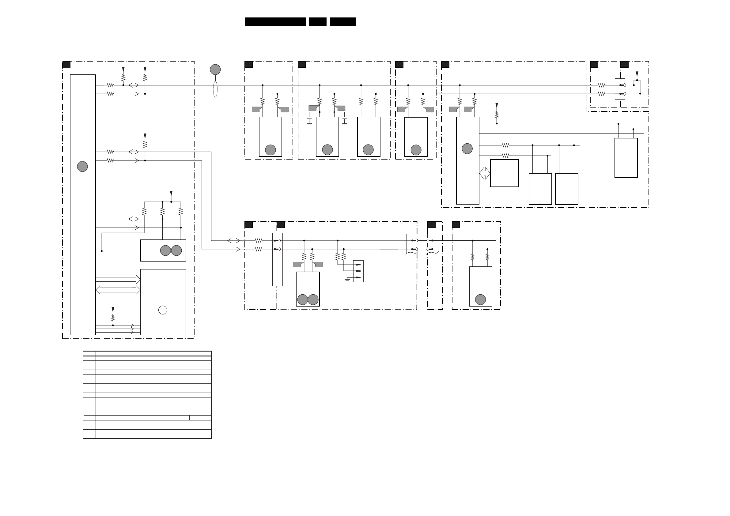
Block Diagrams, Testpoint Overviews, and Waveforms
I2C Overview
23EM1.1A AA 6.
I2C Overview
PAINTER HOP AUDIO
7001
SAA5667HL
SET
PROCESSOR
(PAINTER)
+5V2_CON +5V2_CON
3029
82
3027
81
3032
3033
SDA-F
SCL-F
ERR
6
GENERAL
I2C
+5V2_CON
3031
SDA-S
SCL-S
ERR
12
3028
84
3026
83
+3V3-INTPAINTER
30013074 3002
80
SDA NVM
SCL NVM
78
5
97
WC NVM
7
7012
M24C32
(NVM)
EEPROM
ERR10ERR
6
11
SDA-S
SCL-S
ADDRESS
7011
5
12
28
C47C1019V3332
SRAM
(NVM)
ERR
15
128Kx8
DATA
+3V3_INTPANTER
3061
100
10
9
CEN
WRN
RCN
IF, I/O,
B2 B4 B6
VIDEOPROCESSING
B1
V9
SIMM.
CONN.
3908
3902
3377
47
7323
TDA9320H
HIP
ERR
30
3376
V10
46
A7
12051000
48
49
TUNER, I/O
3201
A69 A70
ERR
C23
TDA9330H
3200 3261 3262
54
1200
TUNER
TEDE9
ERR
13
9
11
7301
HOP
ERR
32
33203321
C22
10
23092310
COMPAIR
CONNECTOR
FOR SERVICE
(REACHABLE VIA
HOLE IN REAR
COVER)
14
7302
TDA9178
TOPIC
(OPTIONAL)
ERR
22
1943
1
2
3
34553454
11
SDA-S
SCL-S
DEMODULATOR
3655
B74
2
7651
MSP3452G
AUDIO
DECODER
ERR
14
1951
1
2
1
3656
B75
1104
1
2
FEATURE BOX
3705
V17V18
54
7709
SAA4978H
PICNIC
ERR
31
CONTROL
N1N2A8B1
SDA-S
SCL-S
3703
1
2
89
88
3132
3
7106
M6232O
I/O
EXPANDER
ERR
35
2
3130
+5P
EPROM
PICNIC
3746
SNERT-DA
SNERT-CL
3702
3739
7716
CLK32
CLK16
26
7714
MSM54V
12222A
FIELD
MEMORY
15
26
7715
MSM54V
12222A
FIELD
MEMORY
SIMM
B1 A8B3B7
CONN.
SIMM
+3V3
12051000
3906
46
3911
47
61 62
7708
SAA4990H
PROZONIC
15
Error Device Description Remarks
1 FBX 3V3 protection FBX 3V3 protection 2 No HFB No Horizontal Flyback
4 5V protection 5V protection
5 No HOP POR Startup failure
6 General IIc bus error General IIC bus error 7 Mains Dip error HW error 9 TEDE9 Turner protection -
MC24C32
10
11 MC24C32 NVM identification error
12 SAA5667 Main uP, int. RAM test failure
14 MSP3451 MSP34xx
15 SRAM test failureCY7C1019
22 TDA9178 Histogram IC
30 TDA9320 HIP I/O video processing
31 SAA4978 PICNIC
32 TDA9330 HOP video control/geometry
M62320
35
NVM communication error
I/O expander HD Jack
-
-
-
-
-
-
-
EM1.1A
only
-
-
-
-
-
CL 36532061_010.eps
020903
Page 24
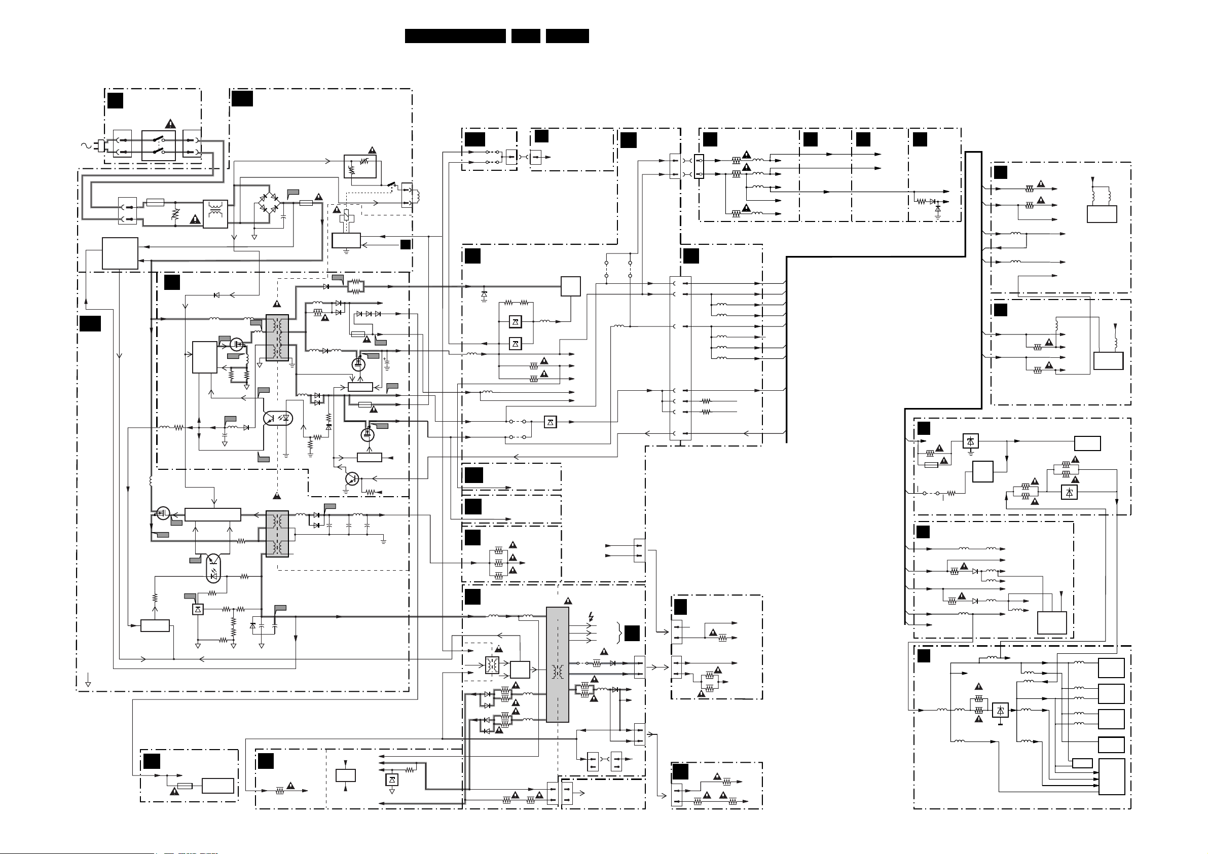
Block Diagrams, Testpoint Overviews, and Waveforms
Supply Lines Overview
24EM1.1A AA 6.
+VBATT
A1B
MAINS
SUPPLY
HOT GROUND
FRONT
J
INTERFACE
0201
OR
0211
2
1
1505
2
1
7505, 7506, 7503
QUICK
SWITCH
OFF
MAIN SUPPLY
SUP-ENABLE
-20V
-20V
SUP-ENABLE
2
1
+375V
3531
ACTIVATING
A5
+11V_ROT
0231
OR
1051
1501
T5AH
5517
7504
STP5NB60FP
D
S
A3
7529
CIRCUIT
ROTATING
CIRCUITRY
0202
OR
0212
2
4
1
3
5502
5503
5504
3509
V
A2
31205106
G
A2
7506
TL431CZP
MAINS
FILTER
STAND-BY SUPPLY
STARTUP
7100
7101
7105
7120
CONTROL
CIRCUIT
-20V
-20V
7502
7530
CONTROL
CIRCUIT
324
A4
7507
TCET1103
3506
A5
1
3
2
SUP-ENABLE
+11V_ROT
1601
1
TDA7052
125mA
A1A
5511
5516
V-START
V-START
6109
7102
STP3NB60
A11
G
A12
5113
3108 3118
GND-STB
A13
5102
2102
GND-STB
MAIN SUPPLY
3514
3520
1
VBATT
ADJUSTMENT
3507
3530
3510
3527
3526
GND-SUPGND-FB
7680
MAIN SUPPLY
6525
GBU4J
4
GND-STB
51095101
A10
3
5104
D
2
S
1
GND-STB
A15
7103 OR
5
6103
4
A16
5506 OR
5
4
3
1
HOT
6514
2523 2515
GND-FB
A4
+11D
2
A1
1503
1
++-
3
2516
5100
65
7
8
10
5103
1
7104
2
3114
5512
5507
6
7
9
10
N.C.
COLD
A6
+VBATT
FRAME
DEFLECTION
E/W DRIVE
3449
+375V
5112
3161
6130
5111
6107
6111
3113
6122
3124
6535
6539
+8Vb
COLD HOT
3550
21
RP
0+
RS
3
1
1550
4
7501
7528
ACTIVATING
CIRCUIT
3115
A17
6110
3116
6113
6117
6118
6148
1148
1A25
5130
+8V6-SWITCH
7131
S
D
STP16NE06
G
7133
7130
CONTROL
1147
1A6
+5V-SWITCH
7141
D
STP16NE06
G
CONTROL
7132
3173
A7
5514
+
+
2512
2546
+VBATT
+141V
+13V-LOT
+13V-LOT
2
+8V-S
7620
TDA8177
4
-15V-LOT
-15V-LOT
8+
2
+5.2V_MP
DEGAUSSING
VTUN
+11V_STBY
6119
+11V_ROT
+11V
A18
A20
A21
S
7140
STANDBY
+11V_STBY
+28V
+
2542
GND-AUD
3
COLD
PAINTER
+8V6
2126
A19
+5.2V
+5.2V_MP
+5V
+8V6
PAINTER
COLD
HOT
7813
1502
HOT
B7
2
1
3635
DEG.
COIL
FRONT
A10
+5V2
+8V
A8
VTUN 9
6200
-C33
5902
+11V
+5V2
+5V
A11
1947
9970
9972
TUNER SIM CONN.
3907
MC78M05
+8V
+8V
5903
INPUTS/OUTPUTS
1
7911
L78L05
7912
9909
9980
3910
OUTIN
STANDBY
3941
3904
0214
J
1
5901
+8VS
HEADPHONE AMPL.
A7
+5V
AUDIO AMPLIFIER
A6
3720
3721
+28V
LINE
A3
DEFLECTION
+VBATT
SUP-ENABLE
HOT
COLD
+5V2
LINE
DRIVE
+11D
COLD
HOT
-15V-LOT
6464
6465
+13V-LOT
6462
6463
+13V-LOT
-15V-LOT
3722
5400 5401
5410
EW
+141V
3464
3465
3462
3498
3463
LINE
OUTPUT
STAGE
13-7701
(AUDIO AMPL.)
7421
5465
5463
3499
MAINS
SWITCH PANEL
+5V2
1200
TEDE9
TUNER
7.3
+5VT
+8V
+8VS
+8VS2
+11V5
+11V
7910
5
1
3
6
1485
HOT COLD
5430
LOT
COLD
HOT
131
3
+3V3OUTIN
9410
8
9
12
+11D +11D
9904
5904
+11V5
+8V
EHT
FOCUS 1
FOCUS 2
3400
6400
FILAMENT
3460
6460
5461
3461
FILAMENT
PULSES
1498
1499
1
1
PANEL ON CRT
NECK
(IF APPLICABLE)
TUNER
A8
SIM CONN.
9203
+3V3
1940
1
6
F
1424 1424
7
2
+11D
TO
3450
3451
5441
1492
1
3
+11D
+5V2
+8V
+5VA
HD PANEL
INPUT/OUTPUTS
N2
1940
1492
4
5
1
6
7
2
1
3
B1
1000
40
43
45
44
46
47
36
F
+8V_+12V
I
1104
+5VS
4
+8VS
5
SIM
5903
5904
5900
5901
5902
3906
3911
STANDBY
CRT
N.C.
3300
3404
3403
DAF
3809
3807 3808
3940
3941
3942
+5V2
+8V
+8V_AUD
+8V_VDP
+5V
+5V_CON
+5V_VDP
+5V_AUD
+3V3_SIM
SDA-F
SCL-F
+8V
SCAVEM
200V
FILAMENT CRT
11VDC
5903
5904
5900
5901
5902
N.C.
+8V
+8V
+8V
5VS
8VS
video
D
audio
1951
+5V
+8V
1205
CONTROL
N1
+5Vs
+8V
video
2x
1x
1x
2x
1x
2x
1x
1x
1x
N3
SYNC
SLICER
+5Vs
+8Vs
6703
MATRIX
N4
+8V
3424
STANDBY
video
VREF
-/C3V9
PAINTER
B7
1003
T315mA
B6
B3
+5VF
+5V2_CON
3054
4007
+3V3_SIM
+5V_AUD
+8V_AUD
+5V
+5V2
4
13
3041
STANDBY-INFO
AUDIO DEMODULATOR
3650
3644
5654
FEATURE BOX
5703 5704
5706
6650
6653
+5VA
1x
2,3
6,7
7001
PAINTER
3719
3720
+5M
B2
+5V_VDP
+8V_VDP
+5V2
+5V2_CON
+8V
B4
+8V_VDP
+5V_VDP
7005
+3V3-INTPAINTER
63
75
+5V_PA
56645669
5651
5652
5653
5798
7713
(OPTINAL)
4
IF/IO
5303
5416
HOP
+3V3_INT
+5V_AUD
+5DA
+5DB
+8V-AUD
5656
+5VF
+5V_PA
2
3070
3071
5702
5705
3464
3400
5701
5799
+8VC
+8VA
3329
3304
MSP3452G
+5VA
+5P
3V3_PA
3V3_INT
+3D
+3A
+5VCOM
+8VP
+8V_VDP
+5VS
5301
3072
3073
7009
42
+5DB
31 1049
7651
AUDIO
PROC.
+8VP
+5V2_CON
+8V_CON
+8V_VDP
+8VS
+5V_VDP
+5VS
8
7012
NVM
5720
5716
20,21
5711
5717
20,21
5713
7701
CL 36532061_011.eps
5407
11
7323
TDA9320H
HIP
TDA9330H
+3V3_PA
32
5,12
149
5409
45
+8VS
7301
HOP
7716
PICNICEPROM
7714
FIELD
MEMORY
7715
FIELD
MEMORY
7708
PROZONIC
7709
PICNIC
020903
3917
5302
Page 25
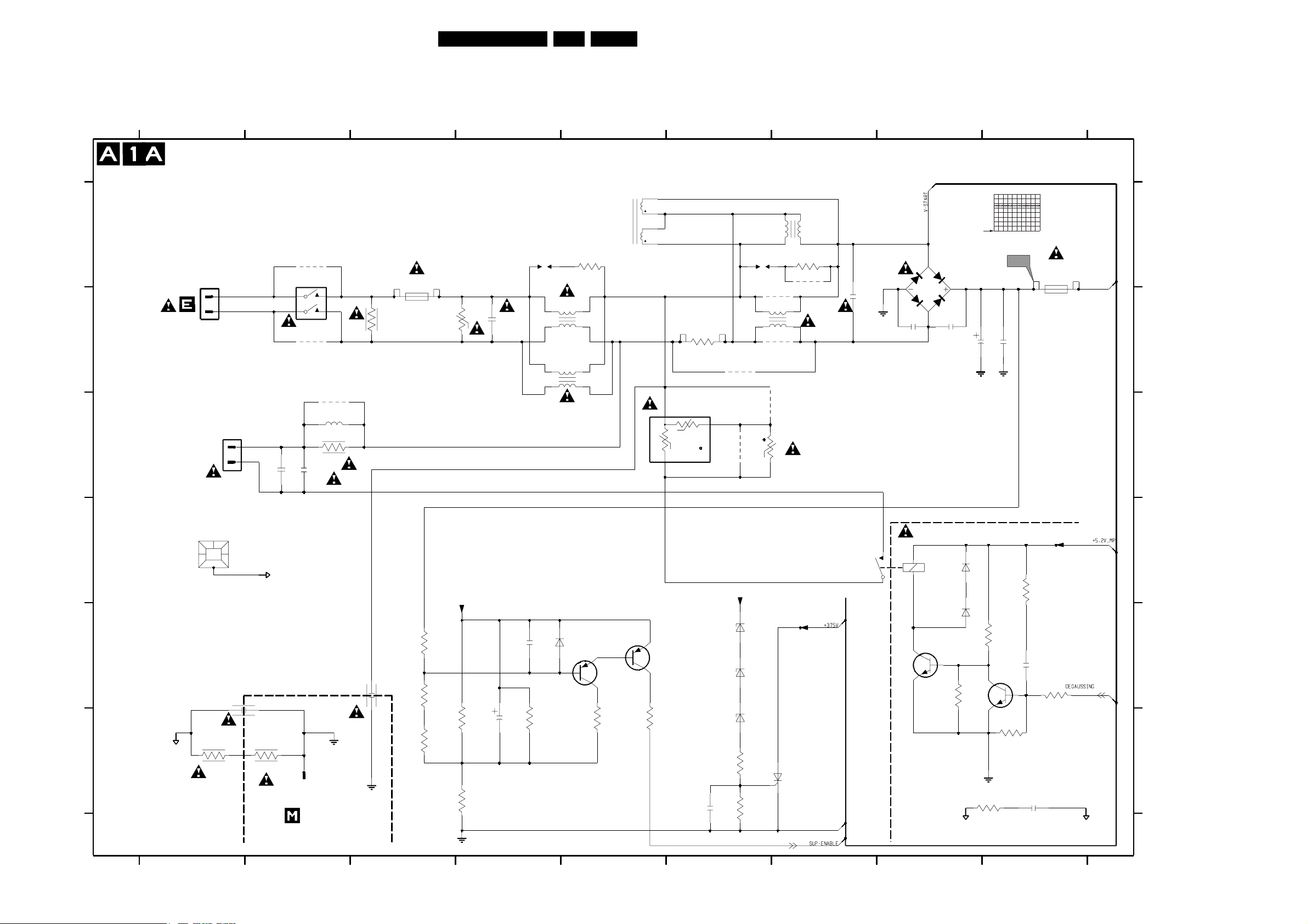
Circuit Diagrams and PWB Layouts
7. Circuit Diagrams and PWB Layouts
Large Signal Panel: Main Supply
25EM1.1A AA 7.
A
B
C
D
E
F
3139 123 5522.2
12 9876543
MAIN SUPPLY
1505
FROM
0202 OF
2
MAINS SWITCH
PANEL
DEGAUSSING
GND-SUP
1
1502
TO
COIL
0043
HEATSINK
123
2505
3503
4M7
HOT
12 9876543
1
2
GND-STB
*
3502
4M7
FOR LATAM - AP SETS
COLD
9501
1500
SDDF
13
RES
24
56
9502
9516
5515
33u
3537
1K
2520
100n
100n
2547
TUNERGND
1510
TO
0301 OF
2521
470p
GND-SSP
T5AH- 250V FOR AP
T6,3AH-250V
3521
4M7
COLD
HOT
1501
for US
3554
6M8
3555
680K
3560
1M2
3509
VBATT
3556
3557
220K
GND-FB
*
47K
0043 D1
1500 A2
1501 B3
1502 C1
A
B
C
1503 A9
1505 A1
1510 F2
1550 D8
1590 A4
1591 A6
2505 E1
2507 B4
2508 B8
2509 B8
2516 B8
2517 B9
2520 C2
2521 E3
2528 E9
2529 F6
2533 F9
2537 B7
2539 F4
2545 E4
2547 C2
3500 B6
3501 A5
3502 F2
3503 F1
3509 B3
3516 C7
5516
54A-0018
1
4
3
2
1590
DSP
2507
V
470n
2
3501
100R
5503
3
14
3500
DSP
1591
23
1
9503
5502
9504
342
4
1
5511
3562
100R
9507
2537
22n
GND-STB
2509
22n
A2-42
GBU4J
6525
2508
22n
1R
2
1
5504
3
4
3550
*
2
232266296
Rs
Rp
+t
1
9513
3
9518
2 9519
+t
3516
1
GND-STB
2516
A1
50V / div DC
2us / div
*
2517
GND-STB
PM3394B
A1
10n
F2,5AH-250V
for AP-PAL
1503
F4AH-250V for
US AP NTSC
143V FOR 120V SETS
277V FOR 230V SETS
A1-8
+375V
7501 E9
7503 F7
7505 E5
7508 E5
7528 E8
9501 A2
9502 B2
9503 B7
9504 B7
9507 A7
9513 B6
9516 C2
9518 C6
9519 C7
3521 B3
3524 E9
3528 E8
VBATT
3
2
1550
14
6511
BAS216
3532
47K
HOT
COLD
A2-43
D
3529 E9
3532 D9
3534 F9
3537 C2
3541 F9
3548 F6
3550 C6
3551 F6
3554 E3
E
F
3555 E3
3556 F4
3557 F4
3558 F5
3559 E5
3560 F3
3561 F4
3562 A7
5502 B7
5503 B5
5504 B5
5511 A7
5515 C2
5516 A5
6507 E6
6508 E6
6511 D8
6512 E8
6513 F6
6522 E5
6525 B8
2539
10u
2545
1n
3561
1M
6522
MCL4148
7505
BC857B
3558
47K
7508
BF423
3559
10K
2529
100n
6507
BZX384-C47
6508
BZX384-C56
6513
BZX384-C56
3548
1K
3551
330R
7503
BT151
GND-FB
A1-8
A3-A4-23
HOT
COLD
7528
BC337-25
3528
10K
GND-SUP
6512
BAS216
7501
3541
3529
4K7
BC847B
GND-SSP
22R
3534
47K
2528
1u
3524
33K
2533
4n7
CL 36532038_083.eps
A8-30
GND-SUP
150703
Page 26
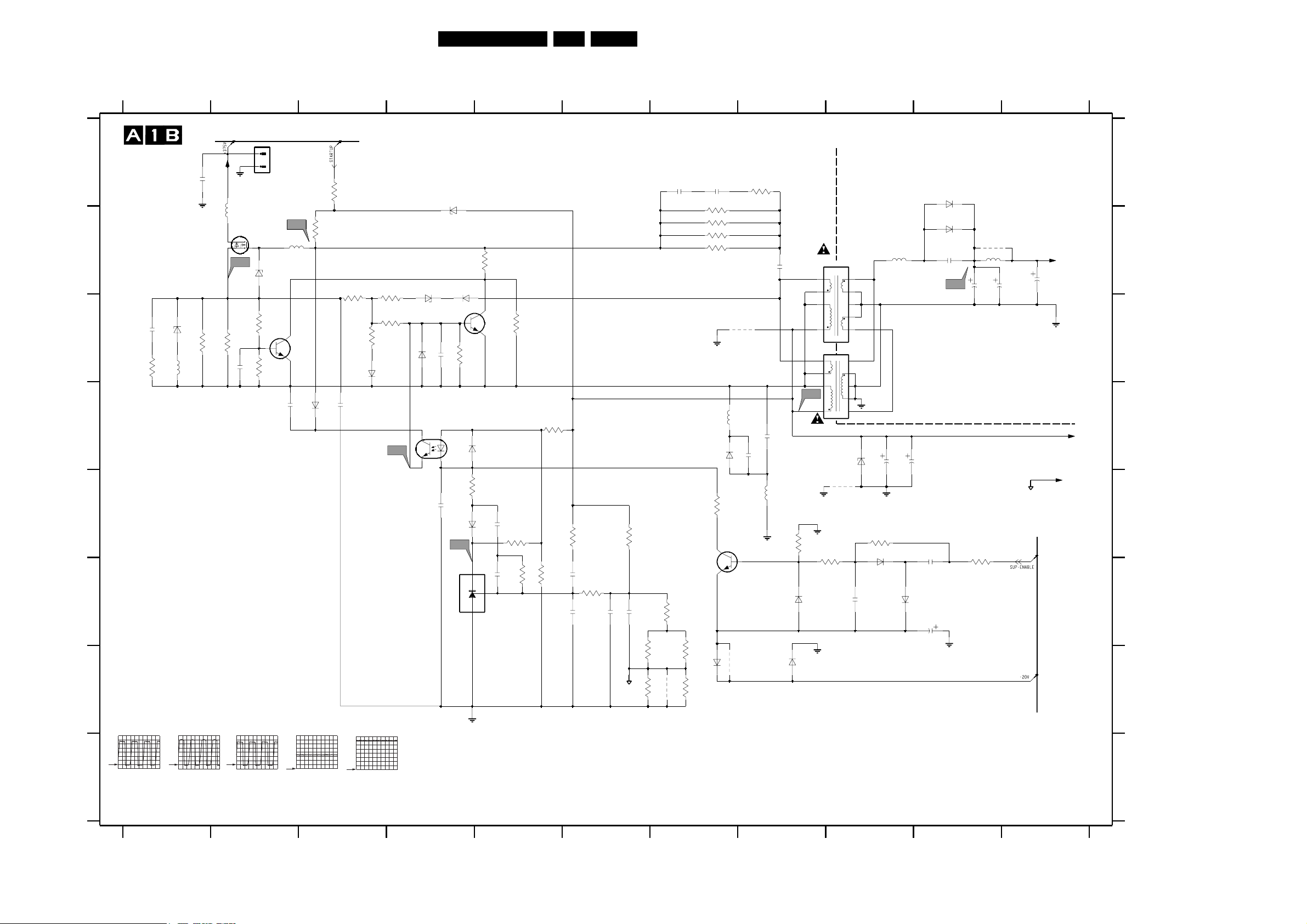
Circuit Diagrams and PWB Layouts
Large Signal Panel: Main Supply
26EM1.1A AA 7.
A
B
C
D
E
F
G
A2
H
50V / div DC
5us / div
3139 123 5522.2
12345678A391011
MAIN SUPPLY
1506
2
2535
4n7
3535
47R
PM3394B
2526
2n2
GND-FB
6515
BZV85-C6V8
5518
A3
50V / div DC
5us / div
3515
*
PM3394B
A1-8
GND-STB
5517
83R
0V
3514
277V
*
A4
50V / div DC
7504
2544
*
5us / div
1
6505
VA
BZX79-C15
3552
*
3553
*
2504
22n
PM3394B
A2
5519
30R
7530
BC847B
A5
5V / div DC
3518
143V
6530
10us / div
*
BYV95C
PM3394B
A2-12
3513
330K
3547
220R
2501
1n
3545
15K
BZX284-C27
3504
2K2
3546
*
6520
1N4148
TCET1103(G)
A4
A6 A7 = +28 VDC
PM3394B
20V / div DC
10us / div
6506
4
3
6518
7507
144V
BZX79-C33
2525
1n5
BAT254
1
2
2538
10n
6510
6519
BYD33D
3505
*
A5
7506
TL431
GND-FB
BAS316
3525
47R
6509
16V6
1
2
0V
3508
15R
7502
BC547B
6538
BAS216
3
2V5
2513
470p
2514
2n2
3512
5K63506
*
3523
1M
3520
33K
3522
6K8
3540
*
2531
2502
10n
*
3530
1K
2506
3507
160K
2524
10n
*
GND-SUP
3527
2K
3542
0R15
3510
820R
9571
*
3539 39K
3538 33K
3544 39K
BC546B
Vbe=0V7
(Vbe=0V)
3549
220K
3526
0R1
25182541
330p
GND-STB
7529
BAS216
2K23511
9511
5520
83R
6534
BY359X-1500
3531
*
2V2
6523
9505
3543
2510
220p
GND-FB
HOT
COLD
2523
47u
2532
1u
BAS216
*
2540
BYV28
6539
6535
STPS8H100
2519
2n2
A7
GND-FB
32V
2546
2m2
3533
15R
9572
33u5514
2512
1m
GND-SUP
+28V
2542
470u
GND-AUD
COLD
HOT
VBATT
GND-SUP
A3-A4-23
A2-44
CL 36532038_084.eps
*
GND-AUD
6514
GND-FB
3536
1K5
6517
BAT254
5507
83R
2515
47u
6516
2527
470p
5505
83R
2503
3517
47K
*
6533
6537
A6
GND-STB
GND-FB
BAS316
GND-FB
BAS216
5512
S419C4-01
69
10
5
11
4
12
132
5506
56
4
3
1
*
3519
9510
2530
7
8
9
10
BZT03-C
1u
030903
A
B
C
D
E
F
G
H
1506 A2
2501 D3
2502 F6
2503 B8
2504 D2
2506 F6
2510 D8
2512 B11
2513 E5
2514 F5
2515 D9
2518 A7
2519 B10
2523 D10
2524 F6
2525 C4
2526 A1
2527 D8
2530 F9
2531 F6
2532 F10
2535 C1
2538 E4
2540 F10
2541 A7
2542 B11
2544 C2
2546 B10
3504 C4
3505 C4
3506 E5
3507 E6
3508 B5
3510 F7
3511 B7
3512 C5
3513 A3
3514 C2
3515 C2
3517 E8
3518 B3
3519 F9
3520 D5
3522 F5
3523 F5
3525 E5
3526 G7
3527 F7
3530 F6
3531 E7
3533 F10
3535 C1
3536 E9
3538 B7
3539 B7
3540 E6
3542 G7
3543 A8
3544 B7
3545 C4
3546 C3
3547 C3
3549 F7
3552 C2
3553 C2
5505 E8
5506 C8
5507 B9
5512 B9
5514 B10
5517 A2
5518 C1
5519 B2
5520 D8
6505 B2
6506 C4
6509 E4
6510 A4
6514 D9
6515 C1
6516 F9
6517 E9
6518 B4
6519 B4
6520 C3
6523 G7
6530 D3
6533 G8
6534 D7
6535 B10
6537 F8
6538 D5
6539 B10
7502 C5
7504 B2
7506 F4
7507 D4
7529 F7
7530 C2
9505 G7
9510 E9
9511 C8
9571 G7
9572 B1
0
1234567891011
Page 27
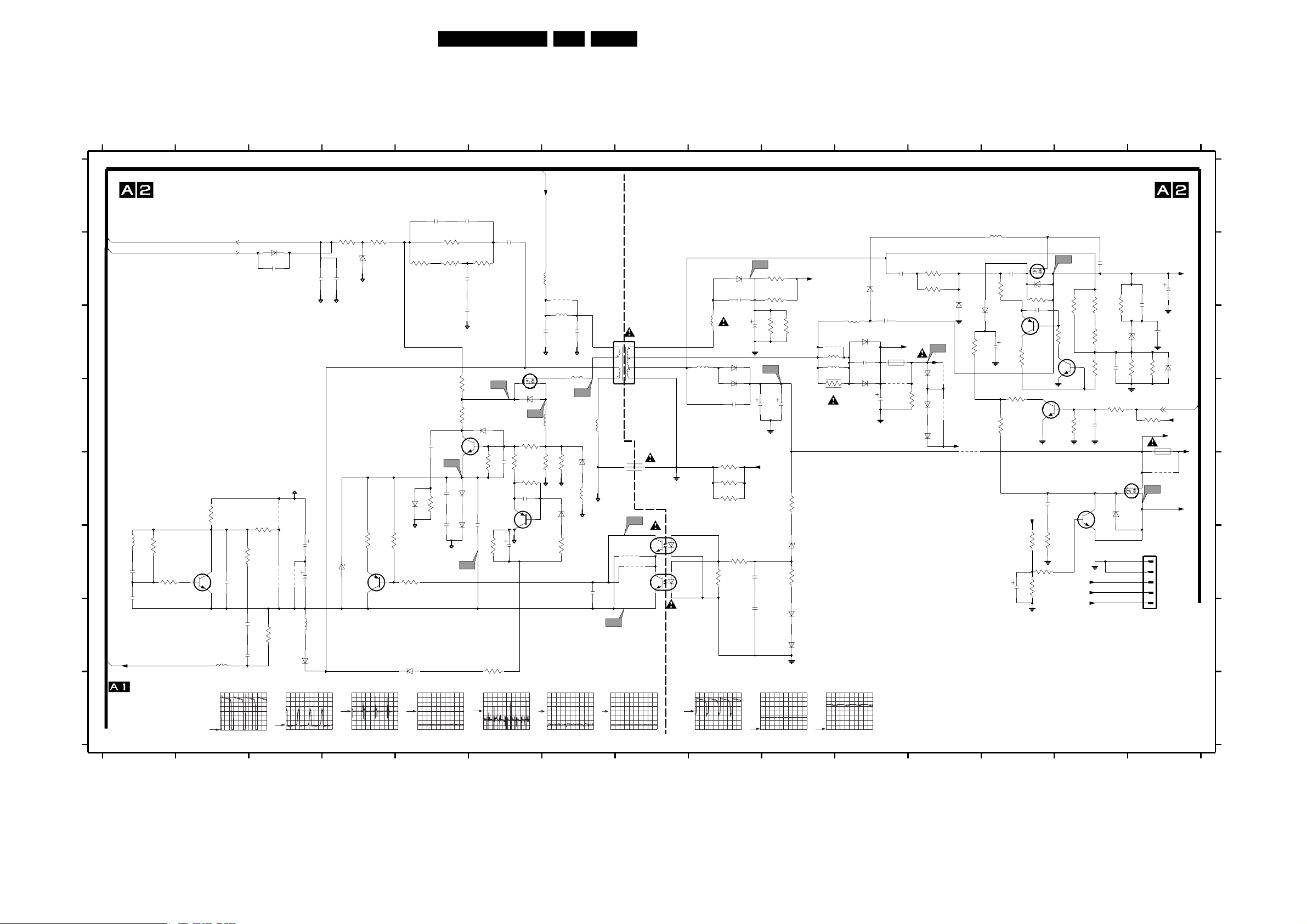
Circuit Diagrams and PWB Layouts
Large Signal Panel: Standby Supply
27EM1.1A AA 7.
A
B
C
D
E
F
G
1146 F15
1147 D15
1148 C11
2100 E8
2101 B6
2102 F3
2103 A5
2104 D9
2105 A5
2106 B15
2107 D9
2108 C6
2109 F9
2110 E5
2111 E6
2112 E6
2114 B4
2115 C9
2116 B9
2118 D11
2119 D10
2120 C11
2121 G2
2122 G2
2123 E6
2124 F6
2126 B15
2130 D14
2131 C13
2132 B14
2140 F13
2141 C13
2143 C11
2144 E5
2145 D5
2147 E13
2148 B11
2149 G9
2150 C14
2151 F3
2152 C7
2153 F7
2154 B13
2155 F1
2156 F1
2157 F2
2159 C5
2160 B5
2161 B3
2162 C15
2163 B4
3101 B4
3102 B5
3103 B6
3104 D6
3105 B5
3106 F3
3107 E2
3108 E7
3109 E9
3111 B5
3113 E10
3114 F9
3115 B10
3116 B10
3117 D5
3118 E7
3120 G3
3121 F3
3123 F10
3124 F9
3125 F4
3126 F4
3127 F5
3130 B13
3131 C12
3132 C13
3133 D15
3134 D14
3135 C14
3136 D13
3137 D11
3138 B4
3140 C14
3141 F13
3142 F13
3143 F13
3144 B12
3145 G6
3146 F7
3147 F6
3148 E6
3149 E6
3150 D6
3151 C14
3152 E5
3153 C14
3155 F13
3156 C14
3157 D14
3158 C15
3159 D13
3160 E6
3161 D10
3162 B12
3164 B13
3165 C15
3166 E9
3167 E9
3168 B14
3169 F1
3170 F1
3171 C10
3172 C10
5100 C7
5101 B6
5102 G3
5103 C9
5104 C7
5105 C10
5106 G2
5107 D7
5108 E7
5109 C7
5110 C9
5111 C11
5112 C10
5113 D7
5130 B13
5131 F1
6103 G3
6104 B4
6105 D6
6106 F4
6107 D9
6108 E5
6109 B3
6110 B9
6111 C9
6112 B13
6113 C11
6114 G5
6115 D6
6116 E7
6117 C12
6118 D12
6119 D12
6120 G10
6121 G10
6122 F10
6130 B11
6132 C14
6133 C12
6134 B12
6141 E14
6142 E5
6144 E5
6147 E7
6148 C11
6149 C15
7100 F4
7101 D5
7102 C6
7103 F8
7104 F8
7105 E6
7120 F2
7130 C14
7131 B13
7132 D14
7133 C13
7140 E14
7141 E14
9101 B7
9102 D12
9103 F8
9106 F8
9107 C12
9108 D12
9112 C10
9122 D11
9123 F3
9126 E15
9128 F3
9129 E3
12 109876543 11 12 13 14 15
HOT
COLD
5100
S22992-02
56
3
2
110
30R
2100
A15
9103
9106
TCDT1102G
15n
A16
A16
7
8
*
4
7104
42
3
5
GND-SSP
TCET1102
1
7103
2
1
5103
A17
BYV27-200
5110
6111
SB360
6107
12
STPS8H100
2107
3n3
3109
680R
3167
680R
3166
680R
3114
220R
PM3394B
6110
2116
100p
3124
68R
A17
GND-SSP
2104
2109
2149
A18
22u2115
3171
A19
2m2
GND-SSP
+5.2V_MP
1u0
1u0
3116
*
3115
*
*
2119
*
3172
2m2
3113
6122
3123
6120
6121
GND-SSP
PM3394B
A8-47
22R
BZX79-B3V9
10R
1N4148
1N4148
35v(0V)
VTUN
A19
9112
5112
83R
5105
3161
100R
5130
13V
83R
STP16NE06
3144
12V
5111
83R
BYW29EX
6113
2143
2n2
2u2
6148
BYV27-200
PM3394B
2148
3n3
220R
+11V_STBY
3137
4K7
6117
6118
6119
3162
470R
A18
A3-48
+11V
BAS316
BAS316
BAS316
6130
STPS8H100
12
2120
1n5
13V1
(0V)
1148
1A25
MP125
9122
2118
1m
GND-SSP
A20 = +8V6 DC A21 = +5 VDC
9107
6134
9108
+11V_ROT
MCL4148
GND-SSP
3131
9102
6133
470R
3130
MCL4148
2141
GND-SSP
3159
2154
33n
47R
7133
BC857B
10u
10K
2140
3136
10R
10V5
3132
47R
18V(0V)
GND-SSP
+8V6
2K7
3141
10u
GND-SSP
7131
6112
BZX384-C10
3164 100K
2131
1n
GND-SSP
3143
100R
3K3
3142
7132
BC847B
2147
3155
GND-SSP
A20
8V5(0V)
+8V SWITCH
3135
100R
BC847B
0V(0V7)
GND-SSP
15n
4V6
(0V)
100R
+5.2V_MP
3140
7130
3157
100K
19v(0V)
7140
BC847B
VTUN
+11V
10K
GND-SSP
3168
3153
3151
2130
4K7
100R
10n
GND-SSP
5V(0V)
A1-12
STARTUP
V-START
A1-42
A1-44
-20V
TO
STAND-BY SUPPLY
5131
3170
100u
47K
2155
100n
3169
1K
2156
10n
7120
BC847B
3107
1K
5106
30R
A10
2157
3n3
2122
2121
PM3394B
1N5062 (COL)
3106
1K
3121
10R
220n
220n
6109
2161
680p
3120
10R
9129
GND-STB
9123
9128
A11
2102
100u
5102
BYD33D
166V
GND-STB
2151
100u
10u
6103
138V
2114
100n
PM3394B
3101
4M7
2163
100n
GND-STB
6106
6104
GND-STB
BZX79-B22
7100
BC557B
A12
3125
3138
1M
PDZ-27B
15R
PM3394B
3126
GND-STB
10K
3127
5K6
6114
BYD33D
MCL41486144
3102
1K
A13
2145
3152 1K
100p
2105
470p
3111
1K5
3105
1K
7101
BC337-25
A14
1u02144
2110
GND-STB
PM3394B
1u0
2103
100p
2159
3117
6142
6108
A13
470p
2160
470p
GND-STB
47R
3104
47R
6115 BAT254
BAT254
BAT254
3103
1K
2111
47n
3160
A14
3145
220R
A11
1K
BC557B
3147
2K2
10n2112
7105
2101
2n2
7102
BZX79-C15
3148
22R
GND-STB
2124
10u
PM3394B
2123
100n
3150
100R
3149
10K
+375V
6105
A12
RES
A1-8
5101
2108
GND-STB
STP3NB60
150V
3108
GND-STB
9101
5109
83R
10n
GND-STB
5113
83R
**
3118
6116
3146
47R
A15
2152
220n
5104
83R
A10
BZX79-C6V8
5108
GND-STB
BZM55-C5V6
5107
6147
GND-STB
2153
2132
2n2
3156
4K7
2150
3134
1K
+5V -switch
STP16NE06
(0V3)
6141
(0V)
100R
6132
10n
3158
GND-SSP
7141
BZM55-C15
2n2
2106
BZX384-C6V8
100R
3165
3133
47K
5V2 (5V3)
A21
5V1 (0V)
1146
1
2
3
4
5
2162
MP160
2126
GND-SSP
1u0
GND-SSP
6149
100R
+11V_STBY
+5.2V
1147
1A6
9126
N.C.
2m2
MCL4148
A8-9
STANDBY
A1-43
+5V
+8V6
+5.2V_MP
A
B
C
D
E
F
G
H
3139 123 5522.2
12 109876543 11 12 13 14 15
50V / div DC
5us / div
5V / div DC
5us / div
2V / div DC
5us / div
5V / div DC
10us / div
200mV / div DC
10us / div
500mV / div DC
5ms / div
5V / div DC
5ms / div
20V / div DC
5us / div
5V / div DC
5us / div
1V / div DC
5us / div
CL 36532038_085.eps
030903
H
Page 28
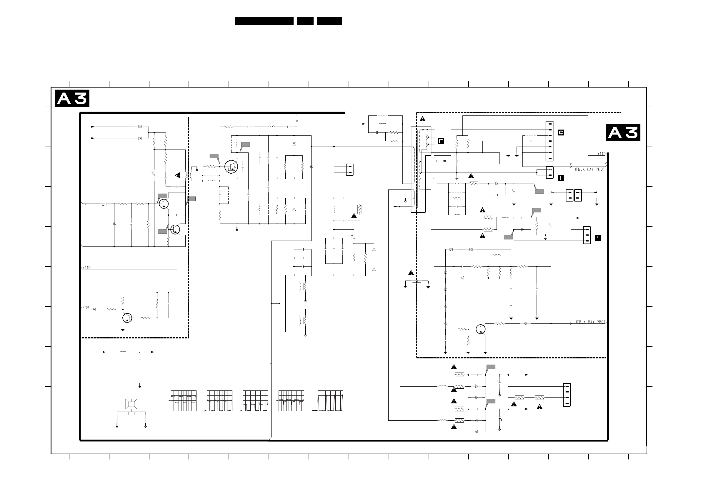
Circuit Diagrams and PWB Layouts
Large Signal Panel: Line Deflection
0040 H2
1492 C13
2400 G2
2412 B3
2418 B5
1417 B7
1424 A12
1430 C9
1491 B13
1493 B10
1495 G13
1498 C13
1499 C13
2401 A8
2402 C12
2405 E9
2409 C3
2413 B3
2414 B3
2415 C2
2417 C4
2419 C6
2420 C5
2421 D6
2422 D6
2423 D6
2424 D8
2425 B5
2426 B5
2430 C7
1234567891011121314
LINE DEFLECTION
A
+11D
+5.2V
11V2
5V2
B
A8-3
LINEDRIVE1
C
GND-LINEDRIVE
A8-4
100u
2492
6406
0V
MCL4148
D
A3-48
E
3440
A6-A8-45
0V
1K
7445
F
VBATT
G
H
123456
GND-SUP
6408
BYD33D
6407
MCL4148
3406
100R
2415
3414
330R
220p
POR-CIRCUIT
22K
3441
0V6
BC847B
5400
33u
2400
0040
HEATSINK
GND-SUP
10V4
2413
0V4
3407
3442
470K
+141V
47u
GND-SUP
2431 C7
2432 D7
2433 D7
2434 D7
2435 B5
3415
10K
3443
15R
10u
3416
3411
47n
A22
0V4
A23
680K
2440 E3
2441 E12
2442 D10
2443 E12
2444 F10
COLD
100R
39R
2412
6V6
7409
BC847B
3404
470R
2440
A22
4
5410
1
2414
47n
2409
47p
6V6
7408
BC368
1u
1V / div DC
10us / div
2445 E12
2450 B10
2460 D13
2461 C12
2462 G11
GND-SUP
A24
PM3394B
HOT
6
CE165T
9
2463 G11
2488 B6
2464 H11
2492 C1
2494 A5
2465 H11
2495 A6
2468 C11
3400 B11
2469 C10
3410
47R
7421
A25
BU2520DX
3409
0V1
1K
9623
5411
560n
9417
220n
2417
10R
3417
GND-SUP
A23
PM3394B
200mV / div DC
10us / div
9426
5426
3401 A9
3402 A9
3404 D3
3406 C2
3407 C2
2494
220n
A26
90R
470p
2418
RES
1n2
A24
5V / div DC
10us / div
2420
3409 B4
3410 A4
3411 B3
3414 C2
3415 A3
*
2425
5425
PM3394B
11n
83R
*
2435
2426
9425
5402
150u
EW
*
9n1
27n
2488
3425
A4-46
3416 A3
3417 C4
3423 B6
3425 C6
3426 C6
430n
10R
RES
A25
2V / div DC
3431 C8
3435 D8
3436 D8
3437 D11
3440 F2
2495
220n
6421
9423
560n
5423
RES
10R
3426
6422
RES
*
*
PM3394B
10us / div
3441 E2
3442 F2
3443 E3
3444 E11
3445 E11
A1-A4-23
SUP-ENABLE
LINE
BY359X-1500
6R8
6423
3423
RES
470p
2419
BY229X-600
2423
470n
*
2422
1u2
*
2421
680n
*
43
21
5424
CU15
GND-SUP
3
5422
CU20
4
12
GND-SUP
28EM1.1A AA 7.
3446 E12
3447 D12
3448 F10
3450 A10
3451 A10
DEFLECTION
BY228/20
2430
3n3
3u6
5421
2431
3n3
*
*
680n
2432
A26:
200 V / div DC
10µs / div
2433
680n
PM3394B
2434
3452 F10
3453 F11
3454 D11
3460 C11
3461 C11
+141V
1417
1
2
LINE
DEFLECTION
COIL
3431
2424
2u2
*
470n
33K
3435
RES
3462 G10
3463 G10
3464 H10
3465 H10
3469 D12
150R
RES
33K
3436
RES
6435
6434
RES
2401
6n8
3498 H12
3499 H12
3689 C10
5400 G2
5401 A8
9401
5401
18u
RES
BYD33J
RES
BYD33J
3401
27R
3402
120R
TO
RES
1430
SIN
5402 A6
5410 B3
5411 B4
5421 C7
5422 F6
1
1
5
4
6
GND-SUP
GND-SUP
5423 B6
5424 E6
5425 C5
5426 A5
5430 A9
2405
1n5
5430
OV2076
8
11
9
123
5461 C11
5463 G10
5465 H10
5466 C10
5469 B10
EHT
FOCUS
G2
CRT PANEL
10
#
#
#
#
TO
1493
#
5463
5465
1
6412
6413
64146415
2444
6400 B11
6401 F12
6406 C2
6407 A2
6408 A2
SIN
RES
RES
6409
3450
2450
5469
9410
3689
1K
2469
3n3
5466
22u
BAS316
BAS316
PDZ-8.2B
PDZ-15B
1u
3462
3463
3464
3465
1R
1R
1R
1R
10K
2442
6n8
6411
RES
3448
2K7
100n
x
#
#
0V4
x
0V
6409 D10
6410 D11
6411 E10
6412 E10
6413 E10
10K
3451
3400
1R
RES
6410
3452
470R
2463
470p
6462
BYW76
6463
BYV29X-500
2465
470p
BYW76
BYV29X-500
3437
10R
6464
6465
x
x
6414 E10
6415 F10
6421 A6
6422 C6
6423 B6
EHT-INFO
3460
3461
x
x
7407
BC817-25
GND-SUP
1R
1R
3444
13V7
#
A31
A32
-15V2
BYV95C
6400
2468
470p
x
3454
1R
1R
3445
3453
100R
2462
2464
6434 E8
6435 D8
6460 C12
6462 G11
6463 H11
5461
A30
RES
x
x
xxx
#
1m
1m
GND-SUP
6464 H11
6465 H11
7407 F11
7408 D3
7409 C3
FILAMENT
33u
2402
2461
470p
6460
BYV95C
FILAMENT PULSES
3447
100R
RES
3446
22n
2441
22n
2445
BAS316
+13V-LOT
3498
5R6
-15V-LOT
6401
9484
7421 B4
7445 F2
9401 A8
9410 C10
9417 C4
0V
0V
-1V4
5V8
0V
0V
233V
0V
0V
A28
A29
1K
3469
2443
560p
3499
5R6
1424
1
2
3
4
5
6
7
1
2
1491
+13V-LOT
9423 B6
9425 C5
9426 A5
9484 A12
9623 B4
2460
13V7
-12V8
CRT
PANEL
VDAF
1m
0V
TO
0224
TO
1491
1
2
3
4
1
2
1495
1498
x
#
x
1499
1
2
NC
+11D
1492
+11D
1
2
3
= AC FILAMENT
= USA XRAY PROT
= DC FILAMENT
N.C
A3-48
A8-20
EHT-INFO
A8-41
+11D+11D
TO
1492
VDAF
A8-41
COLD
HOT
HOT
COLD
A
B
C
D
E
F
G
H
3139 123 5522.2
123456
7 8 9 10 11 12 13 14
CL 36532038_086.eps
030903
Page 29
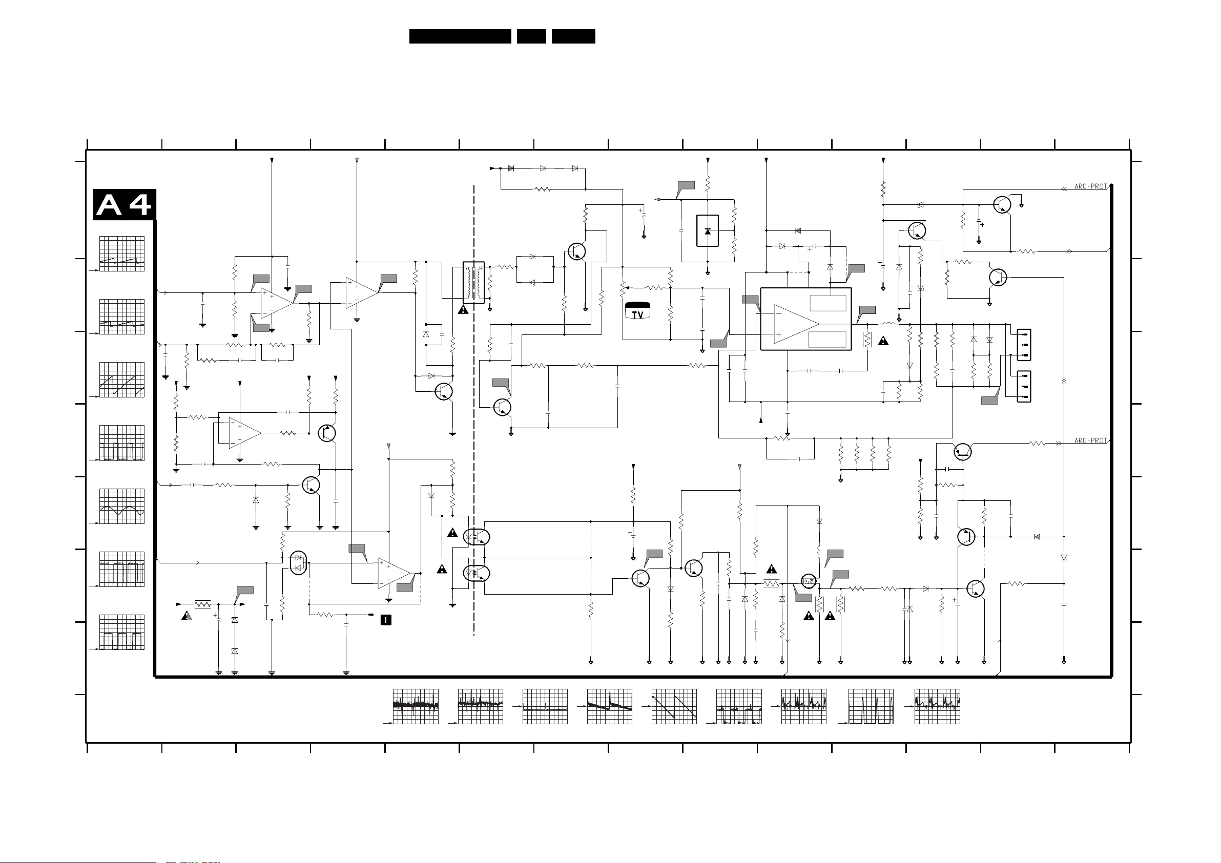
Circuit Diagrams and PWB Layouts
Large Signal Panel: Frame Deflection E/W Drive
8Vb
2657 B3
2659 C2
2660 F11
2661 C8
2662 C3
3403 A13
3412 D5
3418 E9
1625 B13
1627 C13
1693 F4
2403 D3
2404 D2
2448 B12
2451 F2
2454 F3
2457 E4
2458 E2
2466 D12
2480 F9
2481 F9
2482 G10
2487 A13
2490 E8
1234567891011121314
2491 F12
2493 G4
2497 E12
2498 F14
2499 E13
2603 C6
2604 C9
2605 C5
2620 C9
2621 D10
2622 A10
2623 C3
2624 C11
2625 C10
2627 C11
2628 A8
2629 C12
2630 B9
2631 B9
2633 D7
2635 A8
2642 B11
2653 D10
2656 B2
FRAME DEFLECTION
E/W DRIVE
A
A33
PM3394B
10n
A33
3
2
A34
8
4
0V
3657
22K
2623
2n2
2V4
7
3419
470K
MCL4148
15n
2454
2657
1V3
2403
1n
3422
3K3
3458
3486
3487
7440-A
LM358N
7455
PMBT2369
0V5
470R
6K8
1
2
8K2
A35
1
6456
3611
8Vb
3420
7441
BC857B
3
BAV99
2K2
3K3
0V
0V
9405
3654
4K7
(SEE DIAGRAM A3 ALSO)
B
C
D
E
F
G
500mV / div DC
2ms / div
A34
PM3394B
500mV / div DC
2ms / div
A35
PM3394B
500mV / div DC
2ms / div
A36
PM3394B
200mV / div DC
10us / div
A37
PM3394B
500mV / div DC
2ms / div
A38
PM3394B
200mV / div DC
10us / div
A39
PM3394B
2V / div DC
10us / div
NOTE
12K
3664
15K
RES
2656
1V5
1V5
3459
470R
3655
1V1
1K2
3656
1V1
3658
22K
2662
6n8
RES
8Vb
7440-B
5
8
LM358N
6
4
A8-10
FRAMEDRIVE+
A8-11
FRAMEDRIVE-
22n
2659
2K2
3659
8Vb
3K3
3455
3421
470K
6K8
3456
2404
2458
A8-41
560p
HFB_X-RAY-PROT
22n
1n
6455
A8-6
EW-DRIVE
2451
1m
A49
8Vb
6457
+11D
3449
100R
BZX384-C2V7
6458
BZX384-C5V6
BRIDGECOIL PROTECTION (5422) IS TRIGGERED VIA EW
3419 D3
3420 C3
3421 D2
3422 D3
3449 F2
3455 C2
3456 D2
3457 C4
3
1V2
2
1V3
8Vb
3457
2457
1K5
15n
2493
8Vb
A37
3n3
8
4
0V
7V9
1V6
1V2
1693
3458 E3
3459 E2
3466 E12
3467 A12
3472 E12
3474 E13
3475 F11
3476 E12
A36
1
0V4
7450-A
LM393D
8Vb
7V9
5
6
TO
VDAF
8
4
A40
7450-B
LM393D
A38
3478 F11
3479 F10
3480 F11
3481 F10
3482 F9
3483 F9
3484 E8
3485 F7
6K8
3610
MCL4148
BAT254
7
1V2
PM3394B
COLD
7V9
6616
2V6
6614
6615
9481
3486 E3
3487 F3
3488 E9
3489 F10
3490 E5
3491 F12
3492 E8
3493 E8
5621
S13974
56
3
110
GND-SUP
1n
2605
3641
470R
3V5
7614
BC847B
1K8
3412
3K3
3490
MCL4148
7483
0V7
TCET1102
14
0V
15
A41
3495 F13
3496 F8
3497 D13
3610 B5
3611 B3
3620 D11
3621 D11
3622 D11
+8V-S
HOT
3639
A39
-0V9
RES
32
7V8
7482
TCDT1102G
0V6
42
PM3394B
MCL4148
6627
3660
5K6
1K5
3662
56K
2603
4V1
0V1
GND-SUP
MCL4148
MCL4148
220p
7612
BC847B
A42
3623 D10
3624 C11
3625 C12
3626 C12
3627 C12
3628 A7
3629 C12
3630 B8
MCL4148
6618
6617
3632
39K
6626
3628
100R
RES
2633
0V4
3n3
PM3394B
29EM1.1A AA 7.
3631 B7
3632 C7
3633 B7
3634 C9
3635 A9
3636 A9
3637 A9
3638 B8
MCL4148
6625
56K
3633
GND-SUP
GND-SUP
3V
3690
3640
7611
BC847B
1K
RES
RES
3485
A43
2K2
9483
9482
3631
470R
3639 C6
3640 A7
3641 C6
3642 B8
3643 B8
3644 A12
3645 A11
3646 C12
3642
2K2
2661
GND-SUP
BC847B
7487
GND-SUP
PM3394B
GND-SUP
47K
RES
1n
+8V-S
100R
2490
2628
3492
100u
3647 C12
3648 D11
3652 A12
3653 C11
3654 F4
3655 B2
3656 B2
3657 C3
+8V-S
100u
330K
3643
EW
A45
A44
+13V-LOT
A50
2635
12
7613
TL431CZ
3638
470K
33K
3630
GND-SUP
-
FRAME
3493
4K7
3484
BC847B
6482
BAS216
2K7
3496
GND-SUP
PM3394B
3658 C2
3659 C2
3660 B6
3661 C12
3662 B6
3663 C13
3664 C2
3665 B12
100n
3634
39K
150K
7486
2631
2630
3483
3635
5V7
1V
2u2
8V2
1
2
1K8
330R
3
1V9
GND-SUP
2u2
A41
RES
2604
+141V
3482
RES
2n2
2481
2480
A45
3688 G10
3690 C7
5467 F10
5620 B11
5621 A5
6405 A12
6442 B12
6455 E3
22K
3636
10K
3637
220n
3488
100R
4n7
6481
A40
2620
220n
-15V-LOT
680K
3418
BZX284-C15
PM3394B
6456 F3
6457 F2
6458 G3
6480 E10
6481 F9
6482 F8
6483 F10
6491 E13
+13V-LOT
FRAME DEFLECTION
13V7
6620
BYV27-200
7620
TDA8177
VSUP VSUPO
1
IN-
POWER
AMPLIFIER
IN+
7
GND
2621
18K
3623
56K
3481
G
100R
3489 15K
BAT254
47n
3688
2482
GND-SUP
EW
A46
6621
BYD33D
13V5
9620
2
4
-15V2
2625
470n
100n
GND-SUP
2653
3n3
7480
STP3NB60
A46
6483
100K
GND-SUP
A4-46
6493 F12
6494 F12
6499 F14
6614 C5
6615 E5
6616 C5
6617 B6
6618 B6
-3V6
2622
100u
6622
6
FLYBACK
GENERATOR
THERMAL
PROTECTION
GND-SUP
22V5
6480
BYD33D
22V7
5467
D
S
4R7
3479
PM3394B
3
FLYB
A47
2624
470n
3480
9622
BZV85-C
OUT
*
*
3620
A48
GND-SUP
12V3
1R
100R
4R7
A47
A42
5
3621
3478
6619 C11
6620 A10
6621 A10
6622 B10
6623 A11
6624 C12
6625 A7
6626 A7
+141V
GND-SUP
A43
3624
*
1R
3622
3645
2642
GND-SUP
5620
90R
1R5
2627
3R3
3648
3475
4K7
GND-SUP
PM3394B
6627 A6
6628 C13
7440-A B3
7440-B D3
7441 D3
7442 D13
7443 A13
7450-A B4
150K
0V
0V9
6623
100u
2R2
BYD33D
10u
3653
RES
1R
GND-SUP
1n
2660
6405
BZX79-C47
220R
MCL4148
470p
2448
3647
3646
6619
22K
3627
+141V
3476
3472
6493
BAT254
MCL4148
GND-SUP
A48
7450-B F5
7455 D3
7480 F10
7482 F6
7483 E6
7486 F9
7487 F8
7611 A7
7612 D6
7613 A9
7614 C5
7620 B10
7641 A12
7652 B13
7653 F13
7654 E12
PROTECTION CIRCUIT
BC847B
7443
-10V
10u
3467
2487
3665
RES
120R
100R
2629
21V2
2466
100n
3466
4K7
33n
47K
PM3394B
0V3
3629
3652
100R
47R
2491
100R
RES
100n
RES
7654
BC857B
0V3
10u
100K
GND-SUP
7652
BC847B
6624
MCL4148
3661
150R
-11V7
7442
BC857B
21V2
3474
6628
3663
A44
9499
21V1
7653
BC847B
0V
GND-SUP
MCL4148
150R
56K
21V1
BC847B
7641
3644
BZX284-C15
47K
3625
3626
22K
220K
39K
2497
GND-SUP
6494
RES
6442
3491
EW
RES
2499
3495
33K
A4-46
9405 F4
9481 F5
9482 F7
9483 E7
9499 F13
9620 B10
9622 B11
-16V
1625
1
2
3
1627
1
2
3
3n3
3403
100R
GND-SUP
1PS76SB10
(SEE NOTE)
A1-A3-23
SUP-ENABLE
0V7
FRAME
DEFLECTION
COIL
3497
33K
6491
RES
6499
BZX384-C10
2498
470n
GND-SUP
A
B
C
D
E
F
G
3139 123 5522.2
123456789101112 1314
200mV / div DC
2ms / div
200mV / div DC
2ms / div
20V / div DC
2ms / div
10V / div DC
2ms / div
200mV / div DC
2ms / div
1V / div DC
10µs / div
500mV / div DC
10µs / div
50V / div DC
10µs / div
500mV / div DC
10µs / div
CL 36532038_087.eps
150703
Page 30
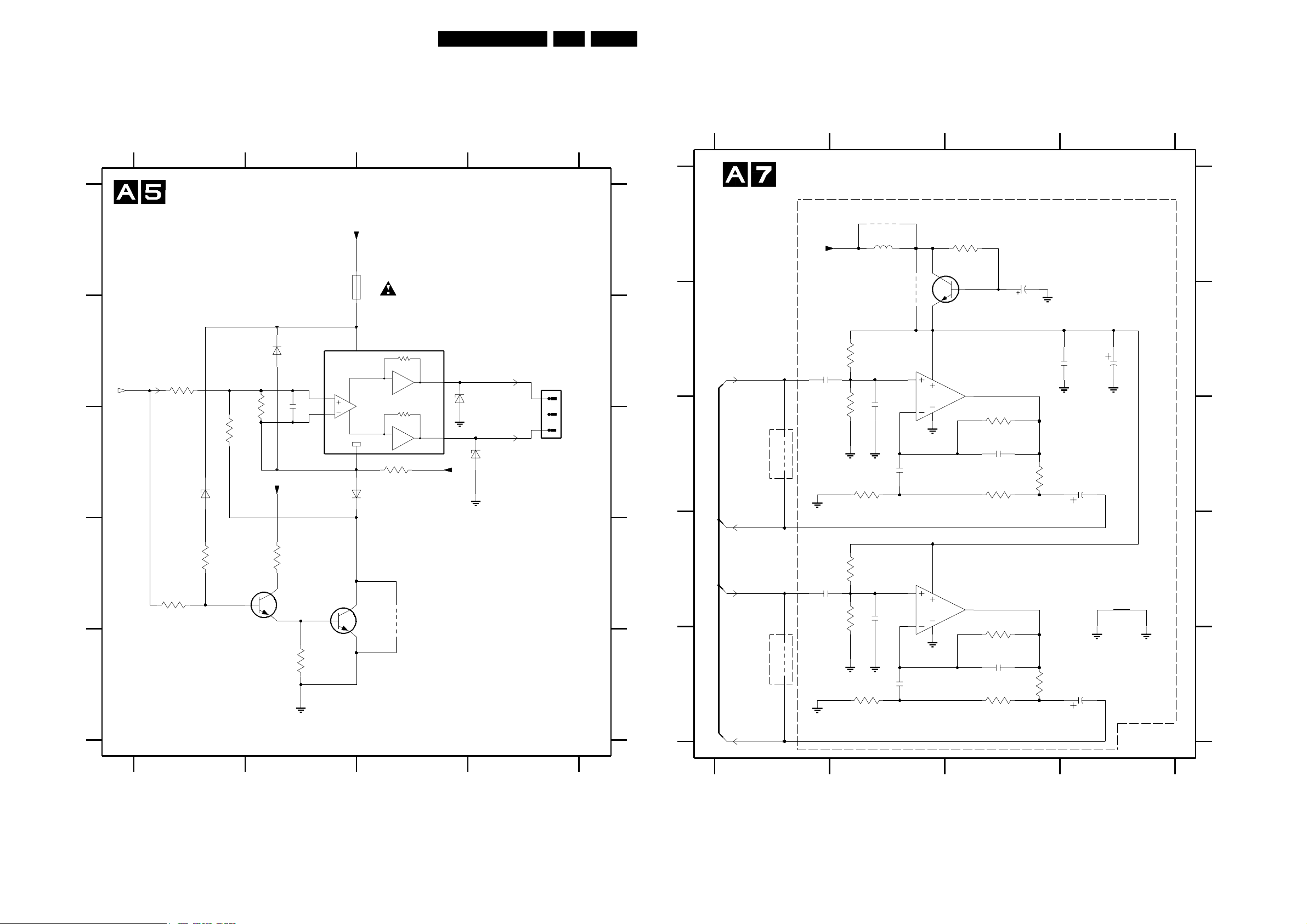
Circuit Diagrams and PWB Layouts
30EM1.1A AA 7.
Large Signal Panel: Rotation Circuitry
1601 A2
1620 C4
2601 B2
3649 D1
3681 D2
3682 E2
3683 D1
3684 B2
1234
ROTATION CIRCUITRY
A
B
FROM A8-49
TILT
3686
56K
3685
27K
3684
BAT254
6K8
C
6084
BZX384-C15
3685 C1
3686 B1
RES
6082
2601
100n
RES
+11V_ROT
3687 C3
4601 D3
+11V_ROT
7680
TDA7052
2
3
OV6
1601
1
+Vp
6080
6080 C2
6081 B3
125mA
13V1
6
OV6
MCL4148
MP13
3687
820R
6082 B2
6083 C4
7
4
+11V_ROT
6084 C1
7680 B2
5
BZM55-C15
8
BZM55-C15
6081
RES
6083
7681 D2
7682 D3
RES
3
OV
2
1
1620
ROTATION
DEFLECTION
COIL
A
B
C
Large Signal Panel: Headphone Amplifier
2751 B4
2752 B4
2754 B1
2755 C4
2756 C3
2757 C2
2758 D1
2759 E4
2760 E3
2761 E2
2762 C2
2763 D2
2764 B3
3752 B2
3753 C2
3754 C3
1234
HEADPHONE AMPLIFIER
3752
100K
47K
3756
12K
9716
5750
0u68
2762
1n
A
B
C
A8-34
HEADPHONE-L
*
A8-37
HEADPH-L
GND-STAR
4704
GND-STAR
+5V
2754
1u
3753
GND-STAR
3
2V5
2
2V5
100n
3755 C3
3756 C2
3757 C3
3758 D2
4705
5V
8
NJM4556AM
4
GND-STAR
2757
3764
470R
7712
BC847B
7751-A
1
3759 D2
3760 E3
3761 E3
3762 E3
2V5
3757
100K
2756
33p
3755
12K
470u10V
2764
GND-STAR
68R
3763 E2
3764 A3
4703 E1
4704 C1
2751
100n
GND-STAR
3754
100u
2755
4705 B2
5750 A2
7712 B3
7751-A B3
FOR EMG-STAR SET
2752
100u
GND-STAR
7751-B D3
9716 A2
c703 D4
A
B
C
D
E
3139 123 5522.2
3683
10K
3649
10K
1V3
3681
OV6
470R
1V2
7681
BC847B
3682
100K
0V1
7682
BC368
0V1
4601
CL 36532038_088.eps
1234
110703
D
E
* FOR A02 SSB
D
A8-35
HEADPHONE-R
E
A8-38
HEADPH-R
3139 123 5522.2
47K
*
4703
2758
1u
GND-STAR
GND-STAR
3758
3759
100K
GND-STAR
3763
12K
2763
2V5
1n
2V5
100n
5V
5
8
6
4
GND-STAR
2761
7751-B
NJM4556AM
7
2V5
12
c703
3762
100K
2760
33p
3761
12K
68R
3760
GND-STAR
100u
2759
GND-AUD
CL 36532038_090.eps
110703
34
D
E
Page 31

Circuit Diagrams and PWB Layouts
Large Signal Panel: Audio Amplifier
1234 56 78 9
AUDIO AMPLIFIER
32V
3724
1u
PM3394B
3720
1R
3721
1R
3722
1R
9722
3707
10K
3719
47K
10K
GND-STAR
3703
1K
3705
1K
3701
1K
A57
500mV / div AC
10K
GND-STAR
10K
10K
GND-STAR
PM3394B PM3394B PM3394B
1ms / div
A
+28V
B
SOUND-ENABLE
A8-2
POR
A8-45
C
AUDIO-R
A8-14
D
AUDIO-SW
A8-19
AUDIO-L
E
A8-13
A56
F
* ONLY FOR SUBWOOFER
3139 123 5522.2
2705
20mV / div AC
1ms / div
1234 56 78 9
3726
50K
3723
GND-STAR
1n
3704
1n
3706
GND-STAR
1n
3702
10K
47K
3708
3711
10K
7710
BC847B
2704
2721
1u
2706
2702
A58
20mV / div AC
200µs / div
2703
220n
470u
2701
220n
100u50V
2722
GND-STAR
A56
2708
A58
47K
7711
BC847B
GND-STAR
A59
500mV / div AC
1ms / div
3710
3716
10K
GND-STAR
1u
2707
GND-STAR
GND-STAR
GND-STAR
3725
4702
10K
9715
14V
9702
14V
14V
GND-SSP
MUTE = 5V
NORMAL = 0V
10 MUTE1
GND-AUD
31EM1.1A AA 7.
7701
TDA7497
1 INR
9 MUTE2
INL
5
INC6
7 SVR
PGND-C
9712
*
32V
*
9710
13
VS2VS-C
OPAMP
CENTER
MUTE/STBY
PROTECT
L/R
OPAMP
OC 3
OPAMP
PGND
SGND
411158
GND-STAR
c701
c702
GND-STAR
2709
GND-STAR
14V
14OR
12OL
14V
14V
1m
GND-STAR
100n
1m
2717
3715
4R7
2710
3714
4R7
1m
2714
1m
2711
3713
4R7
2715
47n
2712
47n
2718
47n
2716
47n
GND-STAR
2713
47n
GND-STAR
2719
47n
GND-STAR
GND-STAR
A59
GND-STAR
GND-STAR
A8-19
AUDIO-SW
GND-STAR
FOR ACTIVE SUBWOOFER
GND-STAR
GND-STAR
A57
SPK-R
SPK-L
FOR PASSIVE SUBWOOFER
1
2
3
5
4
3
2
1
4
3
2
1
1
2
3
1739
N.C.
1740
1735
1738
MAIN SPEAKERS
10W 8E R
10W 8E L
CL 36532038_089.eps
030903
A
B
C
D
E
F
1735 D8
1738 E8
1739 A8
1740 B8
2701 E3
2702 E2
2703 C2
2704 D2
2705 D1
2706 D2
2707 B4
2708 D3
2709 A6
2710 A6
2711 D7
2712 D7
2713 D7
2714 C7
2715 C7
2716 C7
2717 E6
2718 E7
2719 E7
2721 D2
2722 A3
3701 E2
3702 E2
3703 C2
3704 D2
3705 D2
3706 D2
3707 B2
3708 B2
3710 B3
3711 B2
3713 D7
3714 C7
3715 E6
3716 B3
3719 C2
3720 A1
3721 A1
3722 B1
3723 B2
3724 C1
3725 B4
3726 A2
4702 D4
7701 C5
7710 C2
7711 B3
9702 D4
9710 C5
9712 E5
9715 F4
9722 B1
c701 F5
c702 F5
Page 32

Circuit Diagrams and PWB Layouts
Large Signal Panel: Tuner, SIMM Connector (Female)
1234567891011121314
TUNER SIM CONNECTOR (FEMALE)
A
+8V6 +8V
+11V
B
+5V
+5.2V
C
+8V
D
E
F
G
+5VT
1201
TO
1510
SUPPLY
H
GND-LINEDRIVE
components with diversity
*
I
3139 123 5522.2
5902
33u
5903
33u
9980
9909
3910
3907
7V5
1
47R
3904
2915
7912
IN
IN OUT
+8V
GND
MC78M05
GND
7911
L78L05
GND
6R8
10u
TO
1000
68R
OUT
0V
4V9
2201
SIM CONN MALE
4V9
+8VS2
A68
c001
c002
220n
2951
0V
10
11
7
6
+11V5
IN OUT
5901
10u
+8V
3941
2914
FM
2V2
8
NC GND
TUNER
IF1
MB2
MB1
TU2
9
33V
10n
220n
2202
6200
9215
A2-47
VTUN
7910
LD1086
GND
2200
6R8
+8VS
10u
2
TEDE9
1200
AGC
1
BZM55-C33
B-SC1-IN_U-IN
0V
1205
1
+8VS
10u
*
1V7
100u
R-SC1_V-IN
G-SC1-IN_Y-IN
0V
0V
2
3999
1K
100u
2940
+5VT
9906
12131415
5
SDA
4
SCL
AS
3
2203
2950
10n
FBL-SC1-IN
0V
GND-RGB-SC1_YUV
3
+3V3
8V1
7901
BC847B
2V4
9908
3930
560R
1997
1
FROM
2
EXTERNAL
A69
3201
5V
100R
3200
5V
100R
A70
4V9
6201
*
6202
*
3250
22K
C-SC2_SVHS-IN
Y_CVBS-SC2_AV2-IN
CVBS-SC2_MON-OUT
GND-CVBS-IN
0V
0V
0V
2V7
7
9228
9229
9292
2916
330p
3928
3V
100R
10K
3929
CONNECTOR
FM
9
3261
100R
3262
SDA-S
SCL-S
CVBS-SC1_AV1-IN
IF-TER
CVBS-TER-OUT
A11-59
2V7
0V
101112131415161718
GND-CVBS-OUT
0V
0V
0V
GND-CVBS-OUT
AGC
4V1
123456789101112
EHT-INFO
R-SC1_V-IN
G-SC1-IN_Y-IN
B-SC1-IN_U-IN
FBL-SC1-IN
SC1-R_V-IN
A11-53
A11-52
SC1-G-IN_Y-IN
A11-51
CVBS-TER-OUT
TER-CVBS-OUT
SC1-B-IN_U-IN
SC1-FBL-IN
N.C
TO
COMPAIR
1943
SDA-S
1
SCL-S
2
3
100R
1955
SDA-S
1
SCL-S
2
3
N.C.
2V6
A11-69
P50
SC1-STATUS
PIP-CVBS
A8-61
SEL-SVHS-RR_STATUS2
GND-PIP
0V
0V
CVBS-PIP_TUN1-2-CVBS-IN
0V
3V2
19
N.C
Y_CVBS-FRONT-IN
C-FRONT-IN
L-FRONT-IN
FRONT-DETECT
R-FRONT-IN
GND-AUD
HEADPH-L
HEADPH-R
+11V5
HFB_X-RAY-PROT
EHT-INFO
R-CRT
G-CRT
B-CRT
CUTOFF
N.C
CUTOFF
GND-RGB-CRT
0V
5V7
20
21
9989
9990
A7-37
A7-30
+8V
B-CRT
R-CRT
G-CRT
3V
3V
3V
2V5
2223242526
9988
9250
9251
9982
GND-RGB-CRT
A3-4
A3-3
LINEDRIVE1
GND-LINEDRIVE
0V
27
9987
0V
6V
2V8
8V4
3V
3V
3V
0V
5V7
A4-10
A4-11
FRAMEDRIVE-
FRAMEDRIVE+
0V9
1V1
28
29
1934
1
2
3
4
5
6
1933
4
3
2
1
2
1
1965
1936
1
2
3
4
5
6
7
8
9
10
11
1940
1
2
0V
3
4
5
6
7
8
9
10
11
GND
EW-DRIVE
0V
1V6
303132
TO 1934
HD JACK
TO 1933
HD JACK
TO/FROM
SIDE IO
TO
A4-6
A4-41
HFB_X-RAY-PROT
6V
1V4
3427
56K
PANEL
PANEL
N.C.
A11-70
A11-71
0340
CRT
A2-9
A3-20
A5-49
TILT
EHT-INFO
1n
2455
STANDBY
2947
4u7
DYN-FASE-COR
2V3
4V
0V
3334353637
32EM1.1A AA 7.
2496
GND
AUDIO-SL
R-CL_VL-OUT
L-CL_VL-OUT
C-FRONT-IN
Y_CVBS-FRONT-IN
PIP-MONO
PIP-CVBS
TER-CVBS-OUT
CVBS-SC1_AV1-IN
C-SC2_SVHS-IN
Y_CVBS-SC2_AV2-IN
PANORAMA
IRQ-DIGITAL
LIGHT-SENSOR
A10-31
0V
10n
PIP-MONO
2941
100n
0V
5V2
38
394404142
BZX384-C5V6
6901
3428
330K
3429
100K
+5.2V
Y-SCAVEM
2V8
3432
100K
9206
9225
9205
2930
1n
9905
3V2
+8V
2943
100n
2942
8V1
+3V3
3V5
0V
4344454647
1200 F2
9983 C11
1201 G1
9987 B6
1205 I2
9988 B6
1932 F9
A68
PM3394B
200mV / div DC
5us / div
3430
100K
BAS316
6402
2483
4n7
1
2
3
4
5
2931
1n
1
2
3
+8V
9226
1
2
3
1
2
3
4
5
1
2
1
2
SCL-S
SDA-S
+5V
83R
5904
+5VA
+3V3
100n
3V5
5V1
3V5
1961
1953
1952
1935
1932
1966
SDA-S
5V
48
EW-DRIVE
N.C.
TO 0236
OF
2T PIP
DW PANEL
N.C.
TO 0200
OF
2T PIP
DW PANEL
RESERVED
N.C.
A6-2
A3-45
POR
SCL-S
SOUND-ENABLE
5V
0V
0V
495505152
SDA-S
SCL-S
PROT_AUDIOSUPPLY
CVBS-SC2_MON-OUT
A11-55
A11-65
L-SC2_AV2-IN
L-SC1_AV1-IN
0V
0V
0V
535455
VTUN
HFB_X-RAY-PROT
RES
1K
3210
C-FRONT-IN
A11-61
N.C
L-SC2-OUT
L-SC1_AV-OUT
GND-SCART-AV
0V
0V
56
+8V
2K2
3211
7210
BC847B
2929
220n
3938
100R
3939
A11-64
A11-62
R-SC2-OUT
R-SC2_AV2-IN
GND-SCART-AV
0V
0V
0V
58
59660
57
A69
2V / div DC
50us / div
9907
9983
3213
15R
3212
100R
2V7
10K
N.C
R-SC1_AV1-IN
R-SC1_AV-OUT
A11-56
0V0V0V
61
PM3394B
7211
BC847B
3942
100R
8V1
7902
BC847B
2V7
3940
FRONT-DETECT
0V8
62
NOT EUR
3944
AUDIO-SL
+8VS2
10K
3943
8V1
1V7
1V1
2K7
3903
3945
2918
560R
L-FRONT-IN
C-FRONT-IN
Y_CVBS-FRONT-IN
100R
4915
3905
0V
0V
0V
63
65
64
A70
2V / div DC
50us / div
+5.2V
+5VA
10K
+8V
+11V5
VTUN
2917
7908
BC847B
560R
+8VS
100n
A7-34
R-FRONT-IN
HEADPHONE-L
4V5
0V
666768
PM3394B
100n
2944
220n
A11-72
A11-74
A7-35
L-CL_VL-OUT
HEADPHONE-R
4V5
0V
69
SDA-S
SCL-S
9904
9203
9201
9901
9902
9903
NOT EUR
SC2-CVBS_MON-OUT
N.C
AUDIO-C
A11-73
AUDIO-SL
R-CL_VL-OUT
GND-AUD
0V
4V3
0V
0V
7071727374
+5V
+8V
HA
VA
SC2-C-OUT
A11-68
A6-19
A6-13
AUDIO-L
AUDIO-SW
2945
9998
3V5
3V6
75
1
2
3
4
5
1
2
3
4
5
6
7
8
9
10
1
2
3
A6-14
AUDIO-R
2u2
2946
3V5
76
1951
1937
1948
N.C.
A10-27
ON-OFF-LED
2u2
0V
77
TO 1104
N2
OF HD-JACK
PANEL
TO 0201
OF
2T PIP/DW
PANEL
N.C.
N.C.
A1-30
A10-24
A10-25
RC
KEYBOARD
DEGAUSSING
3V
3V3
3V1
78
79880
CL 36532061_039.eps
A
B
C
D
E
F
G
H
.
A11
.
-
-
I
290803
1933 B6
1934 A6
1935 E9
1936 D6
1937 B13
1940 F6
1943 E5
1948 D13
1951 A13
1952 E9
1953 D9
1955 F5
1961 C9
1965 D6
1966 G9
1997 E3
2200 D2
2201 F1
2202 G2
2203 G3
2455 I7
2483 B9
2496 B8
2914 E2
2915 E1
2916 C4
2917 E12
2918 F11
2929 E10
2930 F8
2931 D9
2940 B3
2941 I8
2942 I8
2943 I8
2944 E12
2945 H13
2946 I13
2947 I7
2950 G3
2951 G2
3200 F3
3201 F3
3210 D10
3211 D10
3212 D11
3213 C11
3250 H3
3261 E4
3262 F4
3427 A7
3428 A8
3429 B8
3430 A9
3432 A8
3903 F11
3904 E1
3905 I11
3907 C1
3910 C1
3928 C4
3929 D4
3930 D3
3938 F10
3939 G11
3940 G11
3941 E2
3942 E11
3943 E11
3944 C11
3945 F11
3999 A3
4915 I11
5901 C2
5902 A1
5903 A1
5904 H8
6200 G2
6201 G3
6202 G3
6402 B9
6901 A8
7210 D10
7211 D11
7901 C3
7902 F11
7908 E11
7910 B2
7911 D1
7912 C1
9201 C12
9203 C12
9205 E8
9206 D8
9215 G2
9225 E8
9226 D9
9228 A4
9229 A4
9250 E6
9251 E6
9292 B4
9901 C12
9902 C12
9903 D12
9904 C12
9905 F8
9906 E3
9907 C11
9908 C3
9909 B1
9980 B1
9982 F6
9989 B6
9990 B5
9998 I13
c001 H2
c002 I2
13 14
Page 33

Circuit Diagrams and PWB Layouts
33EM1.1A AA 7.
Large Signal Panel: Receiver
1950 A1 2900 B2 3900 A3 3901 B3 3902 C3 6900 B3
1234
RECEIVER
RES
1950
A
B
C
AGC
CTRL
CIRCUIT
BAND
PASS
M1
M2
45
INP
PIN
RC RECEIVER
DEM
VS 2
OUT 1
GND
3
2900
100u
3900
220R
A71
3901
6900
3902
470R
TLDR5400
1K8
+5.2V_MP
A8-24
A8-27
A
B
C
Large Signal Panel: Front
123
TO
0214
A
FRONT
INTERFACE
PANEL
B
NC
TO
0241
C
MAINS
SWITCH
PANEL
N.C.
D
1947
1949
1946
FRONT
5
4
3
2
1
2
1
1
2
2V
3V1
3
4
5V2
5
0V
0V
6
7
3V3
8
0V
8V2
9
4914
4912
4911
2952
3914
1n
9978
KEYBOARD
ON-OFF-LED
9970
9973
10K
3911
RC
ON-OFF-LED
1K
KEYBOARD
LIGHT-SENSOR
3912
8K2
10K
3913
RC
+5.2V
+8V
+5.2V
RCOUT
+8V
A8-25
A8-27
A8-24
A8-24
A8-27
A8-24
A8-25
A8-31
A
B
C
D
1945 E3
1946 B1
1947 A1
1949 B1
2952 D2
3911 B2
3912 D3
3913 D2
3914 C2
4911 A2
4912 A2
4914 A2
9970 A3
9973 B3
9978 A2
D
3139 123 5522.2
D
CL 36532038_092.eps
021003
1234
E
3139 123 5522.2
KEYBOARD
1945
1
0V
3V3
2
3
0V
A8-25
TO
0215
P
TOP CONTROL
PANEL
CL 36532061_040.eps
290803
123
E
Page 34

Circuit Diagrams and PWB Layouts
Large Signal Panel: Inputs/Outputs
12 78 9
INPUTS/OUTPUTS
1901-A
YKF51-5347
A
8
3
7
2
1
AV2:
CVBS
B
R
L
C
D
AV1:
E
F
3139 123 5522.2
1900-C
1900-A
U
V
CVBS
3
1
1900-B
2
Y
L
R
SVHS-IN:
5104
6
1901-B
9
11
6
1988
4
5
18
15
1900-F
1900-H
14 17
1900-G
13 16
9
1900-I
1900-E
811
1900-D
710
12 78 9
1983
1996
1995
25
12
1994
1993
1992
1990
1989
3950
10K
1991
3969
1K
3970
1K
3958
3960
3962
3964
3965
1K
3966
1K
1987
3968
2998
2999
75R
75R
75R
75R
SEL-SVHS-RR_STATUS2
3996
100R
75R
3995
3967
Y_CVBS-SC2_AV2-IN
100R
75R
100p
100p
3957
100R
3959
100R
3961
100R
3963
100R
2993
2994
CVBS-SC1_AV1-IN
100p
100p
34EM1.1A AA 7.
3 6
A8-69
C-SC2_SVHS-IN
A8-70
A8-71
R-SC2_AV2-IN
A8-64
L-SC2_AV2-IN
A8-65
A8-59
L-SC1_AV1-IN
A8-55
R-SC1_AV1-IN
A8-56
3 6
45
1K
3980
100K
3979
7993
3983
3971
3975
3987
3991
BC847B
27K
100K
7995
BC847B
39K
100K
7991
BC847B
39K
3984
3972
3976
3988
3992
150R
1K
270R
1K
330R
2996
2u2
2995
2u2
4903
2997
2u2
4904
45
3982
10R
4902
3974
10R
3990
10R
3981
3985
180R
3973
3977
470R
3978
3989
3993
100R
3994 3986
1K
BC857B
7992
1K
1K
BC857B
7994
1K
1K
BC857B
7990
1K
SC1-G-IN_Y-IN
A8-52
SC1-B-IN_U-IN
A8-51
SC1-R_V-IN
A8-53
:
A8
2988
SC2-CVBS_MON-OUT
A8-68
L-SC2-OUT
A8-61
R-SC2-OUT
A8-62
AUDIO-SL
A8-73
L-CL_VL-OUT
A8-74
R-CL_VL-OUT
A8-72
100n
2989
100u
3997
150R
3946
150R
3948
150R
5900
5u6
3954
150R
3956
150R
3952
75R
+8VS
2991
2992
2987
2986
2985
330p
330p
330p
330p
330p
3953
150R
3955
150R
3951
150R
3947
150R
3949
150R
AV2 OUT:
1900-L
2124
1984
1900-K
2023
1999
1900-J
1922
1998
AUDIO-OUT
SURROUND
YKC21-2675
1982
YKC21-2675
1981
YKC21-2675
1980
63
1902-C
52
1902-B
41
1902-A
CL 36532038_094.eps
CVBS
L
R
R
110703
1900-A B1
1900-B C1
1900-C B1
1900-D F1
1900-E F1
1900-F D1
1900-G D1
1900-H D1
1900-I E1
A
1900-J C9
1900-K B9
1900-L A9
1901-A A1
1901-B A1
1902-A F9
1902-B E9
1902-C D9
1980 F9
B
1981 E9
1982 D9
1983 D1
1984 B9
1987 A2
1988 B1
1989 C2
1990 B2
1991 B2
C
1992 F1
1993 F1
1994 E1
1995 E1
1996 D1
1998 C9
1999 B9
2985 F8
2986 E8
2987 D8
D
2988 A7
2989 A7
2991 B8
2992 C8
2993 F2
2994 F2
2995 D4
E
F
2996 A4
2997 E4
2998 B2
2999 C2
3946 E7
3947 E8
3948 F7
3949 F8
3950 A2
3951 D8
3952 A8
3953 B8
3954 B7
3955 C8
3956 C7
3957 C3
3958 D2
3959 D3
L
3960 D2
3961 D3
3962 E2
3963 E3
3964 E2
3965 F2
3966 F2
3967 B3
3968 B2
3969 B2
3970 C2
3971 C5
3972 C5
3973 C6
3974 C4
3975 D5
3976 D5
3977 C5
3978 D6
3979 A5
3980 A5
3981 A6
3982 A4
3983 B5
3984 B5
3985 B5
3986 B6
3987 D5
3988 D5
3989 D6
3990 E4
3991 E5
3992 E5
3993 E5
3994 E6
3995 A2
3996 A3
3997 D7
4902 B4
4903 D4
4904 F4
5900 A7
7990 E6
7991 E5
7992 A6
7993 A5
7994 C6
7995 C5
F960 B9
F961 A2
F962 B9
F963 C9
F964 B2
F965 B2
F966 C2
F967 C2
F968 D2
F969 D2
F971 E2
F973 F2
F974 F2
F975 A8
I963 F3
I964 F3
I965 A4
I966 B4
I967 B6
I968 B5
I969 C8
I970 C3
I971 C6
I972 C5
I973 C5
I974 C5
I975 D3
I976 D4
I977 C4
I978 D5
I979 D6
I980 D3
I981 E6
I982 E5
I983 E5
I984 E4
I985 E5
I986 A5
I987 A6
I988 E4
I989 E5
I990 E6
I991 B3
I992 E8
I993 E8
I994 E9
I995 E9
I996 C7
I997 A5
I998 A5
I999 B8
Page 35

Layout LSP (Top Side)
Circuit Diagrams and PWB Layouts
35EM1.1A AA 7.
Page 36

Circuit Diagrams and PWB Layouts
36EM1.1A AA 7.
Mapping Large Signal Panel (Top Side)
0040 C6
0043 C4
1146 E1
1147 E2
1148 E1
1200 E7
1201 E4
1205 E6
1417 B5
1424 A7
1430 B6
1491 A5
1492 A7
1493 A6
1495 B7
1498 A7
1499 D7
1500 A2
1501 B1
1502 A2
1503 B2
1505 A2
1506 B2
1510 C4
1550 B2
1590 A2
1591 B3
1601 E1
1620 D1
1625 B7
1627 B7
1693 C6
1735 E4
1738 E4
1739 D5
1740 D5
1900 D7
1901 C7
1902 E7
1932 D6
1933 D7
1934 D7
1935 D7
1936 D5
1937 E5
1940 E6
1945 E4
1946 E3
1947 E3
1948 E5
1949 E1
1950 B1
1951 E5
1952 E6
1953 D5
1955 E6
1961 E5
1965 D7
1966 D6
2100 D2
2101 C2
2102 D1
2104 E2
2107 D2
2108 B1
2111 C1
2114 B1
2115 D1
2116 D1
2118 D2
2119 E2
2120 E2
2121 D1
2122 D1
2124 C1
2126 E2
2132 E2
2140 E3
2141 E1
2143 D1
2148 D1
2151 D1
2152 D2
2157 C1
2161 B2
2163 B1
2200 E7
2203 E7
2400 A5
2401 A5
2402 A7
2405 A5
2413 C6
2418 B6
2419 C5
2420 B6
2421 A4
2422 A4
2423 A4
2424 B4
2425 B5
2426 B5
2430 B5
2431 B5
2432 B4
2433 B4
2434 B5
2435 B5
2450 A7
2451 C7
2460 A7
2461 A7
2462 C7
2463 C7
2464 B7
2465 B7
2468 A7
2469 A6
2487 A5
2488 B5
2490 C4
2491 A4
2492 D6
2501 C3
2503 C2
2505 C4
2506 D3
2507 A2
2508 B4
2509 B3
2510 C2
2512 E3
2515 C3
2516 B3
2517 B3
2518 C2
2519 E3
2520 A2
2521 B2
2523 C3
2526 C3
2527 C2
2531 D3
2537 B3
2539 B3
2540 D3
2541 C2
2542 E3
2546 E3
2547 A2
2622 B7
2624 B7
2625 B7
2627 B7
2628 C7
2642 A5
2708 D4
2709 D5
2711 E4
2714 D4
2717 E4
2722 C5
2752 D5
2755 D5
2759 D5
2764 C5
2900 A1
2914 E7
2915 D6
2940 E5
2947 E2
2989 E7
3101 C1
3102 C2
3103 C2
3104 C2
3105 C1
3106 C1
3107 C1
3108 C2
3111 C1
3113 D1
3114 D1
3115 E1
3116 E1
3117 C2
3118 C2
3123 D1
3124 D1
3125 C1
3126 C1
3127 C1
3137 E1
3141 E2
3144 D1
3161 D1
3162 D1
3171 D1
3172 D1
3213 E5
3400 A7
3401 A5
3402 A5
3403 A5
3409 B6
3411 C6
3415 C6
3416 C6
3417 B6
3418 B4
3423 B5
3425 B5
3426 B5
3431 B5
3435 B4
3436 B4
3449 D6
3450 A7
3451 A7
3460 A7
3461 A7
3462 B6
3463 B7
3464 B6
3465 B6
3469 A7
3476 A5
3478 C4
3479 C5
3480 C4
3488 B4
3492 C5
3493 B4
3495 A4
3498 B7
3499 B7
3500 A3
3501 A3
3502 C4
3503 C4
3505 D2
3507 D4
3508 C3
3509 A2
3511 C2
3513 C2
3514 C3
3515 C3
3516 B3
3518 C2
3520 D3
3521 A1
3526 D3
3533 D3
3537 A3
3540 D3
3541 C4
3542 D3
3543 C2
3545 C3
3546 C2
3548 C4
3550 B3
3551 C3
3554 B4
3559 B4
3562 B3
3620 C7
3621 C7
3622 C7
3623 C7
3624 B7
3625 B7
3626 B7
3628 C6
3634 B7
3635 C6
3641 C7
3642 B7
3645 A5
3648 C7
3661 B7
3663 B7
3681 E1
3687 E1
3689 A6
3716 D5
3720 C5
3721 C4
3722 C4
3725 D4
3726 C5
3754 D5
3760 D5
3904 D7
3941 E7
3952 D7
3958 D7
3960 D7
3962 D7
3963 D7
3964 D7
3968 C7
3992 D7
3994 D7
3995 C7
5100 D2
5101 B2
5102 C1
5103 D2
5104 C2
5105 D2
5108 C1
5109 C2
5110 D1
5111 D2
5112 D2
5113 C2
5130 E2
5131 D1
5400 C4
5401 A5
5402 B5
5410 C6
5411 C6
5421 B5
5422 A4
5423 B5
5424 A4
5425 B4
5426 B5
5430 B6
5461 A7
5463 B7
5465 B6
5466 A6
5467 B5
5469 A6
5502 A3
5503 B2
5504 A2
5505 C3
5506 D3
5507 E3
5511 A3
5512 D3
5514 E3
5515 A3
5516 A3
5517 C3
5518 C4
5520 C3
5620 B7
5621 C7
5750 C5
5900 E7
5901 E7
5902 E2
5903 E1
5904 E6
6103 C1
6105 C2
6106 C1
6107 D2
6109 B1
6110 D1
6111 D2
6113 D2
6114 C1
6120 D1
6121 D1
6122 D1
6130 E2
6147 C2
6148 D2
6400 A6
6405 A5
6408 D6
6421 C5
6422 C5
6423 B5
6434 B4
6435 B4
6460 A7
6462 B7
6463 C7
6464 B6
6465 C6
6480 C5
6505 C3
6510 C2
6514 C3
6515 C3
6519 C2
6520 C2
6525 B4
6530 C2
6534 C2
6535 E3
6539 E3
6619 B7
6620 B7
6621 B7
6622 B7
6900 A1
7100 C1
7101 C1
7102 C2
7103 D1
7104 D1
7105 B1
7131 E2
7141 E3
7408 C6
7421 C6
7440 C7
7480 C4
7482 C5
7483 C5
7502 D2
7503 C3
7504 C3
7506 D3
7507 D3
7508 B4
7528 B1
7529 D3
7613 C7
7620 B7
7680 E1
7682 E1
7701 D4
7910 E5
7911 E7
7912 E6
9101 C2
9102 E2
9112 D2
9114 C1
9117 D2
9118 E2
9119 E1
9120 E2
9121 E3
9122 E1
9123 C1
9124 D2
9125 E1
9126 E2
9127 C2
9223 E5
9224 E5
9227 E4
9250 D5
9260 D7
9261 D7
9263 D7
9264 C7
9266 D7
9267 D7
9268 D7
9269 C7
9270 D7
9292 E4
9401 A5
9402 B4
9403 B4
9404 B4
9405 C6
9406 A5
9408 B7
9409 A7
9410 A6
9411 A7
9412 D6
9413 D6
9414 D6
9415 D6
9423 B5
9425 B5
9426 B5
9484 A7
9501 A2
9502 A2
9503 A3
9504 A4
9507 A3
9508 C3
9509 C3
9510 C3
9511 C3
9513 B3
9516 A3
9517 C3
9518 B2
9519 B3
9551 B3
9552 D3
9554 C3
9556 D3
9557 D3
9558 D2
9563 C4
9564 C2
9565 B2
9566 D3
9570 D4
9571 D3
9572 E3
9620 B7
9622 B7
9623 C6
9650 B7
9652 A7
9655 A7
9656 A7
9658 B6
9659 B4
9660 B4
9661 B4
9663 B4
9664 B7
9665 C6
9666 C6
9667 B5
9669 C5
9670 C5
9671 B4
9674 A6
9675 A7
9678 A7
9700 D5
9701 E4
9702 D4
9703 D4
9704 D5
9705 D4
9706 D4
9707 D4
9708 C5
9709 D5
9710 D5
9711 D4
9712 D4
9713 D5
9714 D4
9715 E5
9716 C5
9717 C5
9718 D4
9719 E4
9722 C5
9901 E5
9902 E6
9903 E6
9906 E7
9907 E5
9909 E5
9910 D6
9911 D6
9912 D6
9913 D6
9914 D6
9915 D6
9916 D6
9917 D6
9918 D7
9919 D6
9920 D6
9921 D6
9922 D7
9923 D7
9924 D7
9925 D7
9926 D7
9929 E6
9930 E6
9931 E7
9932 E6
9933 E7
9934 E7
9935 E7
9936 E7
9937 E6
9938 E6
9939 E6
9940 E6
9942 E5
9943 E6
9944 E6
9945 E6
9946 E6
9947 E6
9948 D6
9949 D5
9950 E5
9951 E1
9952 E4
9953 E4
9954 E6
9955 E4
9956 E4
9957 B1
9958 B1
9959 E7
9961 D6
9963 E7
9964 E3
9965 E3
CL 36532038_42m.eps
9967 E5
9968 D6
9969 D6
9971 E7
9972 E7
9973 E3
9974 E4
9975 E3
9976 B1
9977 D6
9980 E5
9982 E6
9996 E5
140503
Mapping Large Signal Panel (Bottom Side)
2103 C6
2105 C6
2106 E6
2109 D7
2110 B7
2112 C7
2123 C7
2130 E6
2131 E7
2144 C7
2145 C7
2147 E6
2149 D7
2150 E7
2153 D7
2154 D6
2155 C6
2156 D7
2159 C7
2160 C7
2162 E6
2201 E1
2202 E1
2403 C2
2404 C1
2409 C2
2412 C2
2414 C2
2415 C2
2417 B2
2440 C2
2441 B1
2442 B2
2443 A1
2444 A1
2445 B1
2448 A3
2454 D2
2455 D2
2457 C1
2458 D2
2466 A3
2480 C4
2481 C4
2482 C4
2483 E2
2493 C2
2494 B2
2495 B3
2496 E2
2497 A3
2498 A3
2499 A3
2502 D5
2504 C6
2513 D5
2514 D5
2524 D5
2525 D6
2528 B7
2529 C5
2530 D5
2532 D5
2533 C4
2535 C5
2538 D5
2544 C5
2545 B5
2601 E7
2603 C1
2604 B1
2605 C1
2620 B1
2621 B1
2623 C2
2629 B1
2630 C1
2631 C1
2633 C1
2635 C1
2653 C1
2656 C2
2657 C1
2659 C2
2660 A4
2661 C1
2662 C2
2701 D4
2702 D4
2703 D4
2704 E4
2705 D3
2706 D4
2707 D4
2710 D4
2712 E4
2713 E4
2715 D4
2716 D4
2718 E4
2719 E4
2721 D4
2751 D3
2754 D3
2756 D3
2757 D3
2758 D3
2760 D3
2761 D3
2762 D3
2763 C3
2916 E1
2917 D2
2918 E1
2929 D3
2930 D1
2931 D3
2941 E2
2942 E2
2943 E2
2944 D1
2945 D3
2946 D3
2950 E1
2951 E1
2952 E4
2985 E1
2986 E1
2987 E1
2988 E1
2991 D1
2992 D1
2993 D1
2994 D1
2995 D1
2996 D1
2997 D1
2998 D1
2999 D1
3109 E7
3120 D7
3121 D7
3130 E7
3131 E6
3132 E6
3133 D6
3134 E6
3135 E7
3136 E6
3138 C7
3140 D7
3142 E6
3143 E5
3145 C7
3146 C7
3147 C7
3148 C7
3149 C7
3150 C6
3151 E7
3152 C7
3153 D7
3155 E6
3156 E6
3157 E6
3158 E7
3159 E6
3160 C7
3164 E6
3165 E6
3166 E7
3167 E7
3168 D7
3169 C7
3170 C7
3200 E1
3201 E1
3210 E3
3211 E3
3212 E3
3250 E1
3261 E1
3262 E1
3404 C3
3406 C2
3407 C2
3410 B2
3412 C1
3414 C2
3419 C2
3420 C1
3421 C1
3422 C2
3427 E2
3428 E2
3429 E2
3430 E2
3432 E2
3437 B1
3440 D2
3441 C2
3442 C2
3443 C2
3444 B1
3445 B1
3446 B1
3447 B1
3448 B1
3452 B1
3453 B1
3454 B2
3455 C1
3456 C1
3457 C2
3458 C2
3459 D2
3466 A3
3467 A3
3472 A3
3474 A3
3475 A4
3481 C4
3482 C4
3483 C3
3484 C3
3485 C3
3486 C1
3487 D2
3489 C4
3490 C3
3491 A4
3496 C3
3497 A3
3504 D5
3506 D5
3510 D5
3512 C5
3517 D5
3519 D5
3522 D5
3523 D5
3524 B7
3525 D5
3527 D5
3528 B6
3529 B6
3530 D5
3531 D5
3532 B7
3534 B7
3535 C5
3536 D5
3538 C6
3539 C6
3544 C6
3547 C5
3549 D5
3552 C5
3553 C5
3555 B5
3556 C5
3557 C5
3558 B5
3560 B5
3561 C5
3610 C1
3611 C1
3627 B1
3629 B1
3630 C1
3631 C1
3632 C1
3633 C1
3636 C1
3637 C1
3638 C1
3639 C1
3640 C1
3643 C1
3644 A3
3646 B1
3647 B1
3649 E7
3652 A3
3653 B1
3654 C2
3655 C1
3656 C1
3657 C1
3658 C2
3659 C2
3660 C1
3662 C1
3664 C2
3665 A3
3682 E7
3683 E7
3684 E7
3685 E7
3686 E7
3688 C4
3690 C1
3701 D4
3702 D4
3703 D4
3704 D4
3705 D4
3706 D4
3707 D3
3708 D3
3710 D3
3711 D3
3713 E4
3714 D4
3715 E4
3719 C3
3723 D3
3724 D3
3752 D3
3753 D3
3755 D3
3756 D3
3757 D3
3758 D3
3759 C3
3761 D3
3762 D3
3763 D3
3764 C3
3900 A7
3901 A7
3902 A7
3903 D2
3907 E2
3910 E1
3911 E5
3912 E4
3913 E4
3914 E5
3928 E1
3929 E1
3930 E1
3938 E1
3939 E1
3940 E1
3942 D3
3943 D2
3944 E3
3945 D2
3946 E1
3947 E1
3948 E1
3949 E1
3950 D1
3951 E1
3953 D1
3954 E1
3955 D1
3956 D1
3957 D1
3959 D1
3961 D1
3965 D1
3966 D1
3967 C1
3969 D1
3970 D1
3971 D1
3972 D1
3973 D1
3974 D1
3975 D1
3976 C1
3977 C1
3978 C1
3979 D1
3980 D1
3981 D1
3982 D1
3983 D1
3984 D1
3985 D1
3986 D1
3987 D1
3988 D1
3989 D1
3990 D1
3991 D1
3993 D1
3996 C1
3997 E1
3999 B7
4601 E7
4702 D4
4703 D3
4704 D3
4705 C3
4790 D3
4901 E5
4902 D1
4903 D1
4904 D1
4905 D1
4911 E5
4912 E7
4913 E7
4914 E5
5106 D6
5107 D6
5519 C5
6080 E7
6081 E7
6082 E7
6083 E7
6084 E7
6104 C7
6108 C7
6112 E6
6115 C7
6116 C7
6117 E7
6118 E7
6119 E7
6132 E6
6133 E6
6134 D6
6141 E5
6142 C7
6144 C7
6149 E6
6200 E1
6201 E1
6202 E1
6401 B1
6402 E2
6406 C2
6407 D2
6409 B1
6410 B1
6411 B1
6412 B1
6413 A1
6414 A1
6415 A1
6442 B1
6455 C2
6456 C1
6457 D2
6458 D1
6481 B4
6482 C3
6483 C4
6491 A4
6493 A4
6494 A3
6499 A4
6506 D6
6507 C4
6508 C4
6509 D5
6511 B6
6512 B6
6513 C4
6516 D5
6517 D5
6518 C6
6522 C4
6523 D5
6533 D5
6537 D5
6538 D5
6614 C1
6615 C3
6616 C1
6617 C1
6618 C1
6623 A3
6624 B1
6625 C2
6626 C2
6627 C2
6628 B1
6901 E2
7120 D7
7130 E7
7132 E6
7133 E7
7140 E5
7210 E3
7211 E3
7407 B1
7409 C2
7441 C2
7442 A3
7443 A3
7445 C2
7450 C1
7455 D2
7486 C3
7487 C3
7501 B7
7505 B5
7530 D5
7611 C1
7612 C1
7614 C1
7641 A3
7652 A3
7653 A3
7654 A4
7681 E7
7710 D3
7711 D3
7712 C3
7751 D3
7901 E1
7902 E1
7908 D2
7990 D1
7991 D1
7992 D1
7993 D1
7994 D1
7995 D1
9103 D7
9106 D7
9107 E7
9108 D7
9111 D7
9128 C7
9129 C7
9130 E6
9200 E2
9201 E3
9202 E2
9203 E2
9204 E2
9205 E2
9206 E2
9207 E2
9208 E2
9209 B7
9210 D3
9211 D3
9212 E1
9214 E2
9215 E1
9216 E1
9217 E1
9218 E1
9219 E1
9221 E6
9222 E6
9225 E1
9226 E1
9228 E6
9229 E5
9251 D3
9271 D1
9272 D1
9273 D1
9274 D1
9275 E1
9276 D1
9277 C1
9278 C1
9279 C1
9280 C1
9281 D1
9282 D1
9283 D1
9284 D1
9285 D1
9288 D1
9289 D1
9291 D1
9294 C1
9295 C1
9296 C1
9297 D1
9298 E1
9417 B2
9418 A4
9421 D1
9422 D2
9424 C3
9427 D2
9428 C1
9429 D2
9430 D2
9431 C1
9432 D2
9433 C2
9434 C2
9435 C1
9436 C1
9437 C2
9438 B1
9440 E7
9441 C1
9443 C2
9481 C2
9482 C3
9483 C3
9499 A4
9505 D5
9560 C5
9561 D5
9567 C5
CL 36532038_43m.eps
9621 E7
9624 C3
9676 D2
9677 C1
9904 E3
9905 D2
9908 E1
9927 D2
9928 E3
9960 E4
9962 E4
9966 E5
9970 E5
9978 E5
9979 E5
9981 E1
9983 E2
9985 D1
9986 D1
9987 D1
9988 D1
9989 D1
9990 D1
9991 D1
9992 D1
9993 D1
9994 D1
9997 D2
9998 D3
140503
Page 37

Circuit Diagrams and PWB Layouts
Layout LSP (Overview Bottom Side)
37EM1.1A AA 7.
Page 38

Circuit Diagrams and PWB Layouts
Layout LSP (Part 1 Bottom Side)
38EM1.1A AA 7.
Page 39

Circuit Diagrams and PWB Layouts
Layout LSP (Part 2 Bottom Side)
39EM1.1A AA 7.
Page 40

Circuit Diagrams and PWB Layouts
Layout LSP (Part 3 Bottom Side)
40EM1.1A AA 7.
Page 41

Circuit Diagrams and PWB Layouts
Layout LSP (Part 4 Bottom Side)
41EM1.1A AA 7.
Page 42

Circuit Diagrams and PWB Layouts
Large Signal Panel: Main Supply (Only for FL13B Stylings)
123456789
MAIN SUPPLY
A
FROM
0202 OF
MAINS SWITCH
PANEL
B
DEGAUSSING
C
D
E
GND-SUP
F
3139 123 5752.2
1505
2
1
1502
TO
COIL
1
2
0043
HEATSINK
GND-STB
123
2505
*
3503
4M7
3502
4M7
COLD
HOT
ABOUT DC VOLTAGE MEASUREMENT
Normal
standby ( )
123456789
9501
1500
SDDF
13
RES
24
56
9502
2520
100n
2547
100n
TUNERGND
1510
TO
0301 OF
FOR LATAM - AP SETS
9516
5515
33u
3537
1K
2521
470p
GND-SSP
T5AH- 250V FOR AP
T6,3AH-250V
3521
4M7
HOT
COLD
1501
for US
3554
6M8
3555
680K
3560
1M2
3509
VBATT
GND-FB
*
V
3556
47K
3557
220K
2507
470n
2539
10u
1590
DSP
5503
2
14
5504
2
1
2545
6522
1n
MCL4148
3561
1M
3501
100R
3
3
4
7505
BC857B
3558
47K
42EM1.1A AA 7.
5516
54A-0018
1
4
3
2
7508
BF423
3559
10K
*
2
Rp
1
3500
1R
3550
232266296
Rs
+t
3
2529
100n
DSP
1591
23
14
9513
9518
VBATT
6507
BZX384-C47
6508
BZX384-C56
6513
BZX384-C56
3548
1K
3551
330R
9503
5502
9504
+t
4
3
9519
2
3516
1
7503
BT151
1
5511
2
3562
100R
9507
GND-FB
2537
22n
GND-STB
23
A1-8
HOT
A3-A4-23
COLD
2509
22n
4
1
A2-42
GBU4J
6525
1550
7528
BC337-25
GND-SUP
2508
22n
GND-STB
3528
10K
6511
6512
2516
BAS216
BAS216
7501
*
2517
GND-STB
3529
4K7
BC847B
GND-SSP
3541
22R
3534
47K
A1
10n
2533
F2,5AH-250V
for AP-PAL
1503
F4AH-250V for
US AP NTSC
3532
47K
2528
1u
3524
33K
4n7
A1-8
+375V
A2-8
143V FOR 120V SETS
277V FOR 230V SETS
HOT
COLD
A2-43
A8-30
GND-SUP
E_13950_023.eps
240304
A
B
C
D
E
F
0043 C1
1500 A2
1501 A3
1502 B1
1503 A9
1505 A1
1510 F2
1550 D8
1590 A4
1591 A6
2505 E1
2507 A4
2508 A8
2509 A8
2516 B8
2517 B9
2520 C2
2521 E2
2528 E9
2529 F6
2533 F9
2537 A7
2539 E4
2545 D4
2547 C2
3500 B6
3501 A5
3502 E2
3503 E1
3509 A3
3516 C6
3521 A3
3524 E9
3528 E8
3529 D9
3532 D9
3534 E9
3537 C2
3541 F8
3548 F6
3550 B6
3551 F6
3554 D3
3555 E3
3556 E4
3557 F4
3558 E5
3559 E5
3560 E3
3561 E4
3562 A7
5502 A6
5503 A4
5504 B4
5511 A7
5515 B2
5516 A5
6507 D6
6508 E6
6511 D8
6512 D8
6513 E6
6522 D4
6525 A8
7501 E8
7503 F7
7505 E5
7508 D5
7528 D8
9501 A2
9502 B2
9503 A6
9504 B6
9507 A7
9513 B6
9516 B2
9518 C6
9519 B6
Page 43

Circuit Diagrams and PWB Layouts
Large Signal Panel: Main Supply (Only for FL13B Stylings)
1234567891011
MAIN SUPPLY
1506
2
A
B
C
D
2535
4n7
3535
47R
2526
2n2
GND-FB
6515
BZV85-C6V8
5518
3515
*
A1-8
GND-STB
277V
5517
83R
0V
3514
A3
*
2544
*
1
7504
6505
3552
3553
VA
BZX79-C15
*
*
2504
22n
A2
5519
30R
7530
BC847B
6530
3518
*
143V
BYV95C
A2-12
3513
330K
3547
220R
2501
1n
3546
6520
3545
15K
3504
2K2
*
1N4148
BZX284-C27
6506
TCET1103(G)
4
A4
3
E
F
G
H
3139 123 5752.2
6518
7507
144V
BZX79-C33
2525
1n5
BAT254
1
2
2538
10n
6510
6519
BYD33D
3505
*
A5
7506
TL431
GND-FB
BAS316
3525
47R
6509
16V6
1
2
0V
3508
15R
7502
BC547B
6538
BAS216
3
2V5
2513
470p
2514
2n2
3512
*
5K63506
3523
1M
3520
33K
3522
6K8
3540
*
2531
2502
10n
*
3530
1K
2506
43EM1.1A AA 7.
*
GND-SUP
3507
160K
2524
10n
3527
2K
3542
0R15
3510
820R
9571
*
3539 39K
3538 33K
3544 39K
BC546B
Vbe=0V7
(Vbe=0V)
3549
220K
3526
0R1
25182541
330p
GND-STB
7529
BAS216
2K23511
9511
5520
83R
6534
BY359X-1500
3531
*
2V2
6523
9505
3543
2510
220p
GND-FB
1506 A2
2501 D3
2502 F6
2503 B8
2504 D2
2506 F6
2510 D8
2512 B11
HOT
COLD
*
2503
*
5512
S419C4-01
69
10
5
11
4
12
132
5507
83R
BYV28
6539
6535
STPS8H100
2519
2n2
A7
32V
2546
2m2
9572
33u5514
2512
1m
2542
470u
+28V
GND-AUD
A
B
C
5506
56
2527
470p
5505
83R
4
3
A6
1
GND-STB
9510
7
8
9
10
BZT03-C
GND-AUD
6514
GND-FB
2515
47u
2523
47u
GND-SUP
COLD
HOT
VBATT
GND-SUP
D
E
3517
47K
6533
6537
GND-FB
BAS316
GND-FB
BAS216
*
3519
2530
3536
1K5
6517
BAT254
1u
6516
2532
1u
BAS216
*
2540
GND-FB
3533
15R
A3-A4-23
F
A2-44
G
H
E_13950_024.eps
240304
2513 E5
2514 F5
2515 D9
2518 A7
2519 B10
2523 D10
2524 F6
2525 C4
2526 A1
2527 D8
2530 F9
2531 F6
2532 F10
2535 C1
2538 E4
2540 F10
2541 A7
2542 B11
2544 C2
2546 B10
3504 C3
3505 C4
3506 E5
3507 E6
3508 B5
3510 F7
3511 B7
3512 C5
3513 A3
3514 C2
3515 C1
3517 E8
3518 B3
3519 F8
3520 D5
3522 F5
3523 F5
3525 E5
3526 G7
3527 F7
3530 F6
3531 E7
3533 F10
3535 C1
3536 E9
3538 B7
3539 B7
3540 E6
3542 G7
3543 A8
3544 B7
3545 C3
3546 C3
3547 C3
3549 F7
3552 C2
3553 C2
5505 E8
5506 C8
5507 B9
5512 B9
5514 B10
5517 A2
5518 C1
5519 B2
5520 D7
6505 B2
6506 C4
6509 E4
6510 A4
6514 D9
6515 C1
6516 F9
6517 E9
6518 B4
6519 B4
6520 C3
6523 G7
6530 D3
6533 G8
6534 D7
6535 B10
6537 F8
6538 D4
6539 B10
7502 C5
7504 B2
7506 F4
7507 D4
7529 F7
7530 C2
9505 G7
9510 E9
9511 C7
9571 G7
9572 B10
1234567891011
Page 44

Circuit Diagrams and PWB Layouts
Large Signal Panel: Standby Supply (Only for FL13B Stylings)
3104 D6
3105 B5
3106 E3
3107 E2
3108 E7
3109 E9
3138
1M
15R
3126
3111 B5
3113 E10
3114 F9
3115 B10
3116 B10
3117 D5
6144 MCL4148
GND-STB
10K
3127
5K6
6114
BYD33D
3102
2105
100p
1K
2145
1K3152
A
B
C
D
E
F
G
1146 F15
1147 D15
1148 C11
2100 E8
2101 B6
2102 F3
2103 A5
2104 D9
2105 A5
2106 B15
2107 D9
2108 C6
2109 F9
2110 E5
2111 E6
2112 E6
2114 B4
2115 C9
2116 B9
2118 D11
2119 D10
2120 C11
2121 G2
2122 G2
2123 E6
2124 F6
2126 B15
2130 D14
2131 B13
2132 B14
2140 F13
2141 C13
2143 C11
2144 E5
2145 D5
2147 E13
2148 B11
2149 G9
2150 C14
2151 F3
2152 C7
2153 F7
2154 B13
2155 F1
2156 F1
2157 F2
2159 C5
2160 B5
2161 B3
2162 C15
2163 B4
3101 B4
3102 B5
3103 B6
123456789101112131415
STAND-BY SUPPLY
A1-12
STARTUP
V-START
A1-42
A1-44
-20V
5131
100u
10n
2155
100n
2156
3170
47K
3169
1N5062 (COL)
6109
2161
680p
3107
1K
7120
BC847B
1K
5106
30R
2157
3n3
2122
2121
3121
10R
220n
220n
3106
1K
3120
10R
9129
GND-STB
9128
9123
2102
100u
166V
2151
100u
5102
BYD33D
138V
GND-STB
10u
6103
2114
100n
3101
4M7
2163
100n
GND-STB
6106
6104
GND-STB
BZX79-B22
7100
BC557B
PDZ-27B
3125
TO
3118 E7
3120 G3
3121 F3
3123 F10
3124 F9
3125 F4
3111
3105
470p
BC337-25
2144 1u0
2110
GND-STB
44EM1.1A AA 7.
9102 D12
7131 B13
7102 C6
6144 E5
3126 F4
3134 D14
3127 F5
3135 C14
3130 B13
3136 D13
3131 C12
3137 D11
3132 C13
3138 B4
3133 D15
3140 B14
2103
100p
2101
470p
3103
1K
2111
47n
2n2
7102
A11
BZX79-C15
BAT2546115
3150
100R
3148
1K
22R
3160
2112 10n
3149
10K
2123
100n
7105
BC557B
GND-STB
2124
2K2
10u
3145
220R
1K5
1K
2160
470p
2159
GND-STB
47R
3117
3104
47R
7101
A14
6142
BAT254
1u0
6108
BAT254
A13
3141 F13
3142 F13
3143 F13
3144 B12
3145 G6
3146 F7
+375V
GND-STB
STP3NB60
6105
A12
RES
A1-8
5101
10n
2108
150V
5113
83R
**
3108
GND-STB
3147 F6
3148 E6
3149 E6
3150 D6
3151 C14
3152 E5
9101
5109
83R
3118
6116
3146
47R3147
2152
GND-STB
5104
83R
A10
BZX79-C6V8
5108
GND-STB
BZM55-C5V6
220n
6147
3153 C14
3155 F13
3156 B14
3157 D14
3158 C15
3159 D13
S22992-02
5107
GND-STB
2153
HOT
30R
15n
3160 E6
3161 C10
3162 B12
3164 B13
3165 C15
3166 E9
COLD
5100
56
3
7
2
8
110
2100
*
A15
4
9103
9106
7104
TCDT1102G
42
A16
3167 E9
3168 B14
3169 F1
3170 F1
3171 C10
3172 C10
GND-SSP
TCET1102
3
5
5100 C7
5101 B7
5102 G3
5103 C9
5104 C7
5105 C10
5110
5106 G2
5107 D7
5108 E7
5109 C7
5110 C9
5111 C11
BYV27-200
6110
2116
100p
5112 C10
5113 D7
5130 A13
5131 F1
6103 G3
6104 B4
A17
2115 22u
3171
3116
*
3115
*
*
GND-SSP
6111
5103
SB360
6107
12
STPS8H100
2107
3n3
3109
680R
3167
680R
3166
680R
1
7103
2
1
3114
220R
3124
68R
2109
2149
2104
GND-SSP
+5.2V_MP
A19
2m2
2119
1u0
1u0
6105 D6
6106 F4
6107 C9
6108 E5
6109 B3
6110 B9
*
3172
2m2
3113
6122
3123
6120
6121
GND-SSP
A8-47
22R
BZX79-B3V9
10R
1N4148
1N4148
6111 C9
6112 B13
6113 C11
6114 G5
6115 D6
6116 E7
35v(0V)
VTUN
9112
5112
5105
3161
100R
83R
2u2
6117 C12
6118 D12
6119 D12
6120 G10
6121 G10
6122 F10
5111
83R
BYW29EX
BYV27-200
6130 B11
6132 C14
6133 C12
6134 B12
6141 E14
6142 E5
12V
6130
STPS8H100
12
2120
1n5
6113
2143
2n2
6148
2118
1m
GND-SSP
13V1
1148
1A25
MP125
9122
(0V)
2148
3n3
3137
4K7
6147 E7
6148 C11
6149 C15
7100 F4
7101 D5
+11V_STBY
6117
6118
6119
3144
220R
3162
470R
7103 F8
7104 F8
7105 E6
7120 F2
7130 C14
A18
A3-48
+11V
9107
BAS316
BAS316
BAS316
6134
9108
+11V_ROT
GND-SSP
9102
7132 D14
7133 C13
7140 E14
7141 E14
9101 B7
6133
MCL4148
3131
470R
5130
83R
3130
MCL4148
2141
GND-SSP
3159
9103 F8
9106 F8
9107 C12
9108 D12
9112 C10
2154
33n
47R
7133
BC857B
10u
3136
10R
10K
2140
13V
STP16NE06
10V5
3132
47R
GND-SSP
10u
GND-SSP
9122 D11
9123 F3
9126 E15
9128 F3
9129 E3
7131
BZX384-C10
2131
1n
GND-SSP
18V(0V)
+8V6
2K7
3141
3143
100R
3K3
3142
6112
100K3164
2147
3155
+8V SWITCH
7132
BC847B
15n
100R
GND-SSP
A20
8V5(0V)
3135
100R
BC847B
0V(0V7)
GND-SSP
4V6
(0V)
+5.2V_MP
3140
7130
3157
7140
BC847B
100K
10K
19v(0V)
VTUN
+11V
3168
3153
3151
2130
GND-SSP
2132
2n2
4K7
4K7
100R
10n
GND-SSP
(0V3)
5V(0V)
3156
10n
2150
GND-SSP
3134
1K
+5V -switch
7141
STP16NE06
6141
BZM55-C15
(0V)
100R
6132
3158
2n2
2106
2162
BZX384-C6V8
100R
3165
3133
47K
5V2 (5V3)
A21
5V1 (0V)
1146
1
2
3
4
5
2126
1u0
GND-SSP
6149
100R
1147
1A6
MP160
9126
N.C.
2m2
GND-SSP
MCL4148
STANDBY
+11V_STBY
+5.2V
A1-43
+8V6
A8-9
+5V
A
B
C
D
+5.2V_MP
E
F
G
H
3139 123 5752.2
12345678910111213
E_13950_025.eps
14 15
H
240304
Page 45

Circuit Diagrams and PWB Layouts
Large Signal Panel: Line Deflection (Only for FL13B Stylings)
2440 F3
0040 H2
1417 B8
1424 A13
1430 C9
1491 C13
1492 D14
1493 B10
1495 H13
1498 C13
1499 C14
2400 G2
2401 B8
2402 C12
2405 E10
2409 D3
2413 C3
2414 C3
2415 D2
2417 C4
2418 B5
2419 D7
2420 C5
2421 E7
2422 E7
2412 C3
1234567891011121314
2423 E7
2424 D8
2425 B5
2426 C6
2430 C8
2431 D8
2432 E7
2433 E7
2434 E8
2435 B6
2441 F12
2442 E11
2443 F12
2444 G10
2445 F12
2450 B10
2460 D13
2461 D12
2462 H11
2463 H11
2464 I11
2465 I11
2468 C11
2469 C10
2488 B6
2492 D2
2494 A5
2495 A6
3400 C11
3401 B9
3402 B9
3404 D3
3406 C2
3407 D3
3409 B4
3410 A5
3411 B3
3414 C3
3415 B3
3416 B3
3417 D4
3423 B7
3425 D6
3426 D6
3431 D8
3435 E8
3436 E8
3437 E11
3440 F2
3441 F2
3442 F3
3443 F3
3444 E11
3445 E11
45EM1.1A AA 7.
3446 E12
3447 E12
3448 G11
3450 B10
3451 B11
3452 G11
3453 F12
3454 E11
3460 D11
3461 D11
3462 H11
3463 H11
3464 H11
3465 I11
3469 D12
3498 H12
3499 H13
3689 C10
5400 G2
5401 A9
5402 A6
5410 C4
5411 C4
5421 D7
5422 F7
5423 B6
5424 E6
5425 D5
5426 B5
5430 A10
5461 D12
5463 H10
5465 I10
5466 D10
5469 C10
6400 C11
6401 F12
6406 D2
6407 B3
6408 A3
6409 E10
6410 E11
6411 E11
6412 E10
6413 F10
6414 F10
6415 F10
6421 B6
6422 D6
6423 B7
6434 E8
6435 E8
6460 D12
6462 H11
6463 H11
6464 I11
6465 I11
7407 G11
7408 D4
7409 C3
7421 B5
7445 F2
9401 A9
9410 C10
9417 C5
9423 B6
9425 D6
9426 B5
9484 B12
9623 C4
A
+11D
+5.2V
11V2
5V2
6408
BYD33D
6407
MCL4148
10V4
3415
15R
COLD
3416
100R
HOT
3410
47R
B
7421
A25
39R
3411
10u
2413
47n
2412
C
6V6
A8-3
LINEDRIVE1
D
GND-LINEDRIVE
A8-4
A3-48
100u
2492
6406
0V
3406
100R
MCL4148
2415
3414
330R
220p
A22
7409
10K
A23
0V4
BC847B
3404
470R
0V4
3407
2414
47n
2409
47p
6V6
7408
BC368
GND-SUP
6
5410
CE165T
14
9
A24
3409
9623
5411
560n
BU2520DX
0V1
1K
9417
2417
220n
10R
3417
GND-SUP
9426
5426
90R
2418
A26
2494
220n
1n2
470p
RES
2420
*
2425
5425
11n
83R
*
2435
2426
9425
E
POR-CIRCUIT
22K
3441
3440
F
G
A6-A8-45
VBATT
0V
1K
7445
0V6
BC847B
5400
33u
2400
H
0040
23456
1
I
GND-SUP
GND-SUP
3443
3442
470K
+141V
47u
GND-SUP
HEATSINK
680K
2440
1u
3139 123 5752.2
5402
150u
EW
*
9n1
27n
2488
3425
RES
A4-46
430n
10R
2495
220n
5423
3426
560n
RES
10R
RES
6421
9423
6422
*
*
A1-A4-23
SUP-ENABLE
LINE
BY359X-1500
6R8
6423
3423
RES
2419
470p
BY229X-600
2423
470n
*
2422
1u2
*
2421
680n
*
43
21
5424
CU15
GND-SUP
5422
CU2012
43
GND-SUP
DEFLECTION
1
680n
*
3u6
2433
5421
680n
2
2430
3n3
2431
3n3
2434
BY228/20
*
2432
+141V
1417
LINE
DEFLECTION
COIL
3431
2424
2u2
*
470n
3435
RES
33K
RES
150R
3436
RES
33K
6435
6434
RES
2401
6n8
9401
5401
18u
RES
BYD33J
RES
BYD33J
3401
27R
3402
120R
TO
RES
1430
SIN
1
1
5
4
6
GND-SUP
GND-SUP
2405
1n5
5430
OV2076
1424
0V
EHT
TO
FOCUS
G2
CRT PANEL
10
1493
8
11
9
123
#
6412
#
6413
#
6414
#
6415
#
2444
SIN1
RES
6409
3450
2450
5469
9410
3689
1K
2469
3n3
5466
22u
RES
BAS316
BAS316
PDZ-8.2B
PDZ-15B
1u
2442
6n8
6411
RES
3448
2K7
10K
100n
x
#
x
#
3451
6410
3452
RES
10K
3400
1R
470R
3437
10R
EHT-INFO
BYV95C
6400
2468
470p
3460
1R
3461
1R
x
3454
x
x
1R
3444
7407
BC817-25
#
1R
3445
3453
100R
#
x
x
5461
RES
x
A30
x
xxx
33u
2402
2461
470p
6460
BYV95C
FILAMENT PULSES
3447
100R
RES
3446
22n
2441
22n
2445
BAS316
FILAMENT
6401
9484
-1V4
5V8
233V
A28
A29
3469
2443
0V
0V
0V
0V
0V
1K
560p
TO
1
0224
2
3
4
CRT
5
PANEL
6
7
1
TO
2
1491
1491
VDAF
1498
1
2
1m
2460
= AC FILAMENT
x
= USA XRAY PROT
#
x
= DC FILAMENT
1499
+11D
+11D
A3-48
EHT-INFO
+11D+11D
1
2
NC
1492
1
2
3
COLD
HOT
E_13950_026.eps
240304
5463
5465
3462
1R
3463
1R
3464
1R
3465
1R
0V
0V4
2463
470p
6462
BYW76
6463
BYV29X-500
2465
470p
6464
BYW76
6465
BYV29X-500
A31
GND-SUP
13V7
A32
-15V2
2462
2464
1m
1m
GND-SUP
+13V-LOT
3498
5R6
-15V-LOT
3499
5R6
13V7
+13V-LOT
-12V8
1495
1
2
0V
N.C
3
4
HOT
COLD
A8-20
A8-41
TO
1492
VDAF
A8-41
A
B
C
D
E
F
G
H
I
LINE DEFLECTION
1 2 3 4 5 6 7 8 9 10 11 12 13 14
Page 46

Circuit Diagrams and PWB Layouts
Large Signal Panel: Frame Deflection & E/W Drive (Only for FL13B Stylings)
1625 C13
1627 D13
1693 G4
2403 D3
2404 E2
2448 B12
2451 G2
2454 G3
2457 E4
2458 E2
2466 E12
2480 G9
2481 F9
2482 G10
2487 A13
2490 F8
1234567891011121314
2491 G12
2493 G4
2497 F12
2498 G14
2499 F13
2603 C6
2604 D9
2605 C5
FRAME DEFLECTION
A
B
C
D
E
F
G
H
E/W DRIVE
NOTE
BRIDGECOIL PROTECTION (5422) IS TRIGGERED VIA EW
A8-10
FRAMEDRIVE+
A8-11
FRAMEDRIVE-
22n
8Vb
A8-41
HFB_X-RAY-PROT
A8-6
EW-DRIVE
+11D
2659
3455
3456
3659
3K3
6K8
2458
560p
2K2
3421
470K
22n
2404
1n
3449
100R
2620 D9
2621 D10
2622 B10
2623 C3
2624 C11
2625 C10
2627 D11
2628 A8
2656
3664
15K
RES
1V5
2451
3658
22K
8Vb
1V5
5
6
3459
470R
1m
6457
BZX384-C5V6
12K
3655
1K2
3656
1V1
2662
6n8
RES
8
4
A49
BZX384-C2V7
6458
2629 D12
2630 C9
2631 C9
2633 D7
2635 B8
2642 B11
2653 E10
2656 C2
A33
3
1V1
2
A34
7440-B
LM358N
6455
8Vb
8Vb
8
4
0V
3657
22K
2623
2n2
2V4
7
3419
470K
MCL4148
15n
2454
2657
1V3
7440-A
LM358N
2403
1n
3422
3K3
3458
3486
3487
2657 B3
2659 C2
2660 G11
2661 D8
2662 C3
3403 B13
3412 E5
3418 F9
10n
A35
1
3611
8Vb
3420
7441
BC857B
7455
PMBT2369
0V5
0V
470R
6K8
1
3
2
BAV99
6456
9405
8K2
(SEE DIAGRAM A3 ALSO)
2K2
3K3
3654
4K7
0V
3419 E3
3420 D3
3421 D2
3422 D3
3449 G2
3455 D2
3456 E2
3457 D4
1V2
1V3
8Vb
3457
2457
3
2
1K5
15n
2493
8Vb
A37
COLD
6K8
7V9
6616
MCL4148
2V6
6614
BAT254
6615
1V2
9481
3486 F3
3487 G3
3488 E9
3489 G10
3490 E5
3491 G12
3492 E8
3493 F8
5621
S13974
56
3
110
GND-SUP
1n
2605
3641
470R
3V5
7614
BC847B
1K8
3412
3K3
3490
MCL4148
7483
0V7
TCET1102
14
0V
15
3495 F13
3496 G8
3497 D13
3610 B5
3611 C3
3620 E11
3621 E11
3622 E11
+8V-S
HOT
1K5
56K
3639
A39
-0V9
RES
32
7V8
7482
TCDT1102G
0V6
42
MCL4148
6627
3660
5K6
3662
2603
4V1
7612
BC847B
0V1
GND-SUP
MCL4148
MCL4148
6618
6617
MCL4148
220p
3623 E10
3624 C11
3625 C12
3626 D12
3627 D12
3628 A7
3629 C12
3630 C8
6626
3628
100R
RES
3632
39K
A36
1
0V4
8Vb
7V9
TO
VDAF
8
4
7450-B
LM393D
A38
3478 F11
3479 G10
3480 G11
3481 F10
3482 F9
3483 G9
3484 F8
3485 G7
3610
7
3458 E3
3459 E2
3466 E12
3467 A12
3472 F12
3474 F13
3475 F11
3476 E12
8
7V9
7450-A
4
LM393D
0V
5
1V6
6
1V2
1693
3n3
2633
0V4
MCL4148
56K
3n3
GND-SUP
3631 C7
3632 C7
3633 C7
3634 C9
3635 A9
3636 A9
3637 B9
3638 B8
6625
3V
3633
GND-SUP
3690
3640
7611
BC847B
1K
RES
RES
3485
9483
9482
2K2
3631
470R
46EM1.1A AA 7.
3639 C6
3640 A7
3641 C6
3642 B8
3643 B8
3644 B12
3645 A11
3646 C12
3642
2K2
2661
GND-SUP
BC847B
7487
GND-SUP
GND-SUP
47K
RES
1n
+8V-S
100R
2490
2628
3492
100u
3647 C12
3648 E11
3652 B12
3653 D11
3654 G4
3655 B2
3656 C2
3657 C3
+8V-S
100u
330K
3643
EW
A45
+13V-LOT
A50
2635
12
7613
TL431CZ
3638
470K
33K
3630
GND-SUP
-
FRAME
3493
4K7
3484
BC847B
6482
BAS216
2K7
3496
GND-SUP
3658 C2
3659 C2
3660 B6
3661 D12
3662 B6
3663 D13
3664 C2
3665 B12
100n
3634
39K
150K
7486
2631
2630
3483
3635
5V7
1V
8V2
1
2
2u2
1K8
330R
3
1V9
GND-SUP
2u2
A41
RES
+141V
3482
RES
2481
2480
3636
3637
2604
2n2
3688 G10
3690 C7
5467 F10
5620 C11
5621 B5
6405 A12
6442 B12
6455 E3
22K
10K
A40
2620
220n
-15V-LOT
3488
680K
100R
4n7
6481
BYD33D
2
GND
4
2621
GND-SUP
2653
STP3NB60
G
6483
EW
6621
13V5
9620
-15V2
2625
470n
100n
3n3
7480
A46
100K
GND-SUP
A3-46
6493 F12
6494 G12
6499 F14
6614 D5
6615 E5
6616 C5
6617 B6
6618 B6
-3V6
2622
100u
6622
6
FLYBACK
GENERATOR
THERMAL
PROTECTION
GND-SUP
22V5
6480
BYD33D
22V7
5467
D
S
3479
6456 G3
6457 G2
6458 G3
6480 F10
6481 G9
6482 G8
6483 G10
6491 F13
+13V-LOT
FRAME DEFLECTION
13V7
6620
BYV27-200
7620
TDA8177
VSUP VSUPO
1
IN-
POWER
AMPLIFIER
IN+
7
220n
18K
3623
56K
3418
3481
100R
3489 15K
BAT254
BZX284-C15
47n
3688
2482
GND-SUP
BZV85-C
3
FLYB
2624
470n
*
A47
A48
4R7
3480
9622
OUT
3620
6619 C11
6620 B10
6621 B10
6622 B10
6623 B11
6624 C12
6625 A7
6626 A7
A42
12V3
5
3624
*
*
1R
3621
3478
100R
4R7
GND-SUP
+141V
A43
1R
3645
2642
GND-SUP
GND-SUP
5620
1R5
2627
3R3
3622
GND-SUP
90R
3648
3475
4K7
6627 A6
6628 C13
7440-A C3
7440-B D3
7441 D3
7442 E13
7443 A13
7450-A C4
150K
0V
0V9
6623
100u
2R2
BYD33D
10u
3653
RES
1R
GND-SUP
1n
2660
6405
BZX79-C47
220R
MCL4148
470p
2448
3647
3646
6619
22K
3627
+141V
3476
3472
6493
BAT254
6494
RES
MCL4148
GND-SUP
7450-B F5
7455 E3
7480 F10
7482 F6
7483 F6
7486 F9
7487 G8
7611 B7
7612 D6
7613 B9
7614 D5
7620 B10
7641 B12
7652 B13
7653 G13
7654 F12
PROTECTION CIRCUIT
BC847B
7443
-10V
10u
3467
2487
6442
3491
21V2
2466
100n
3466
4K7
3665
RES
120R
100R
33n
0V3
3629
2629
47K
47R
2491
3652
100R
100R
RES
100n
7654
BC857B
0V3
100K
BC847B
MCL4148
3661
RES
21V2
10u
GND-SUP
7652
6624
150R
-11V7
7442
BC857B
3474
6628
3663
A44
9499
21V1
7653
BC847B
0V
GND-SUP
MCL4148
150R
56K
21V1
EW
BC847B
7641
3644
BZX284-C15
47K
3625
3626
22K
220K
39K
2497
GND-SUP
RES
2499
3495
A3-46
33K
-16V
1625
1
2
3
1627
1
2
3
3n3
9405 G4
9481 G5
9482 F7
9483 F7
9499 F13
9620 B10
9622 B11
GND-SUP
3403
100R
1PS76SB10
(SEE NOTE)
A1-A3-23
SUP-ENABLE
0V7
FRAME
DEFLECTION
COIL
3497
33K
6491
RES
6499
BZX384-C10
2498
470n
GND-SUP
A
B
C
D
E
F
G
H
3139 123 5752.2
1234567891011
E_13950_027.eps
12 13 14
240304
Page 47

Circuit Diagrams and PWB Layouts
47EM1.1A AA 7.
Large Signal Panel: Rotation Circuitry (Only for FL13B Stylings)
1601 A2
1620 C4
2601 C2
3649 D1
3681 D2
3682 E2
3683 D1
3684 C2
3685 C1
3686 B1
3687 C3
4601 D3
6080 C2
6081 B3
6082 B2
6083 C4
6084 C1
7680 B2
1234
ROTATION CIRCUITRY
+11V_ROT
A
1601
MP13
125mA
B
C
FROM A8-49
TILT
3686
56K
6084
3649
27K
3685
BZX384-C15
10K
3684
BAT254
6K8
2601
RES
+11V_ROT
3681
470R
6082
RES
100n
7680
TDA7052
2
3
OV6
+Vp
6080
1
6
MCL4148
13V1
OV6
3687
820R
7
4
+11V_ROT
5
BZM55-C15
8
BZM55-C15
6081
D
OV6
1V2
7681
BC847B
3682
100K
0V1
7682
BC368
0V1
4601
3683
10K
1V3
E
3139 123 5752.2
123
RES
6083
7681 D2
7682 D3
RES
3
OV
2
1
1620
ROTATION
DEFLECTION
COIL
E_13950_028.eps
4
120304
A
B
C
D
E
Large Signal Panel: Headphone Amplifier (Only for FL13B Stylings)
2751 B4
2752 B4
2754 B1
2755 C4
2756 C3
2757 C2
2758 D1
2759 E4
2760 E3
2761 E2
2762 C2
2763 D2
2764 B3
3752 B2
3753 C2
3754 C3
3755 C3
3756 C2
3757 C3
3758 D2
3759 D2
3760 E3
3761 E3
3762 E3
3763 E2
3764 A3
4703 E1
4704 C1
4705 B2
5750 A2
7712 B3
7751-A B3
1234
HEADPHONE AMPLIFIER
FOR EMG-STAR SET
A
+5V
9716
5750
0u68
4705
3764
470R
7712
BC847B
10V
470u
2764
GND-STAR
B
47K
A8-34
HEADPHONE-L
C
A8-37
HEADPH-L
* FOR A02 SSB
D
A8-35
HEADPHONE-R
E
3139 123 5752.2
A8-38
HEADPH-R
*
4704
*
4703
2754
1u
GND-STAR
GND-STAR
2758
1u
GND-STAR
GND-STAR
3752
3753
100K
GND-STAR
3756
12K
47K
3758
3759
100K
GND-STAR
3763
12K
2762
2763
1n
100n
1n
100n
3
2V5
2
2V5
GND-STAR
2757
5
2V5
6
2V5
GND-STAR
2761
5V
7751-A
8
NJM4556AM
4
5V
7751-B
8
NJM4556AM
4
2752
2751
100n
2V5
1
3757
100K
2756
33p
3755
12K
7
2V5
3762
100K
2760
33p
3761
12K
GND-STAR
68R
3754
68R
3760
GND-STAR
100u
2755
c703
GND-STAR
100u
2759
7751-B D3
9716 A2
c703 D4
100u
GND-AUD
E_13950_030.eps
120304
A
B
C
D
E
123
4
Page 48

Circuit Diagrams and PWB Layouts
Large Signal Panel: Audio Amplifier (Only for FL13B Stylings)
123456789
AUDIO AMPLIFIER
50K
3723
GND-STAR
1n
3704
1n
3706
GND-STAR
1n
3702
3726
10K
47K
7710
BC847B
2704
2706
2702
3708
3711
10K
2721
2703
220n
1u
2722
A56
2708
470u
2701
220n
A58
100u50V
GND-STAR
7711
GND-STAR
47K
BC847B
3710
3716
10K
GND-STAR
32V
3720
1R
3721
1R
3722
A
+28V
1R
9722
B
3724
3707
10K
3719
47K
10K
SOUND-ENABLE
A8-2
POR
A8-45
C
GND-STAR
AUDIO-R
A8-14
3703
1K
10K
GND-STAR
D
AUDIO-SW
A8-19
2705
1u
3705
1K
10K
AUDIO-L
E
A8-13
3701
1K
10K
GND-STAR
F
1u
2707
GND-STAR
GND-STAR
GND-STAR
3725
4702
10K
9715
14V
9702
14V
14V
GND-SSP
MUTE = 5V
NORMAL = 0V
9 MUTE2
10 MUTE1
5 INL
7 SVR
GND-AUD
7701
TDA7497
1 INR
INC6
PGND-C
*
48EM1.1A AA 7.
CENTER
411
9712
c701
c702
32V
*
9710
13
VS2VS-C
OPAMP
MUTE/STBY
PROTECT
L/R
OPAMP
OPAMP
PGND
15 8
GND-STAR
GND-STAR
OC 3
SGND
2709
GND-STAR
14V
14OR
12OL
14V
14V
1m
2710
100n
GND-STAR
1m
2717
3715
4R7
3714
4R7
1m
2714
1m
2711
3713
4R7
2715
47n
2712
47n
2718
47n
2716
47n
GND-STAR
2713
47n
GND-STAR
2719
47n
GND-STAR
GND-STAR
A59
GND-STAR
GND-STAR
A8-19
AUDIO-SW
GND-STAR
FOR ACTIVE SUBWOOFER
GND-STAR
GND-STAR
A57
SPK-R
SPK-L
FOR PASSIVE SUBWOOFER
1
2
3
5
4
3
2
1
4
3
2
1
1
2
3
1739
N.C.
1740
1735
1738
MAIN SPEAKERS
10W 8E R
10W 8E L
A
B
C
D
E
F
1735 D8
1738 E8
1739 A8
1740 B8
2701 E3
2702 E2
2703 C2
2704 D2
2705 D1
2706 D2
2707 B4
2708 D3
2709 A6
2710 A6
2711 D7
2712 D7
2713 D7
2714 C7
2715 C7
2716 C7
2717 E6
2718 E7
2719 E7
2721 D2
2722 A3
3701 E2
3702 E2
3703 C2
3704 D2
3705 D2
3706 D2
3707 B2
3708 B2
3710 B3
3711 B2
3713 D7
3714 C7
3715 E6
3716 B3
3719 C2
3720 A1
3721 A1
3722 B1
3723 B2
3724 C1
3725 B4
3726 A2
4702 D4
7701 C5
7710 C2
7711 B3
9702 D4
9710 C5
9712 E5
9715 F4
9722 B1
c701 F5
c702 F5
* ONLY FOR SUBWOOFER
3139 123 5752.2
123456789
E_13950_029.eps
240304
Page 49

Circuit Diagrams and PWB Layouts
Large Signal Panel: Tuner SIMM Connector (Female) (Only for FL13B Stylings)
1 2345678910111213
TUNER SIM CONNECTOR (FEMALE)
A11-53
A11-52
A11-51
A11-60
1943
1
2
3
1955
1
2
3
N.C.
PIP-CVBS
GND-PIP
0V
SC1-STATUS
A8-61
0V
A11-69
SEL-SVHS-RR_STATUS2
0V
EHT-INFO
R-SC1_V-IN
G-SC1-IN_Y-IN
B-SC1-IN_U-IN
FBL-SC1-IN
SC1-R_V-IN
SC1-G-IN_Y-IN
SC1-B-IN_U-IN
SC1-FBL-IN
A11-54
Y_CVBS-FRONT-IN
C-FRONT-IN
L-FRONT-IN
FRONT-DETECT
R-FRONT-IN
GND-AUD
HEADPH-L
HEADPH-R
+11V5
HFB_X-RAY-PROT
EHT-INFO
R-CRT
G-CRT
B-CRT
CUTOFF
A11-67
P50
CUTOFF
0V
3V2
5V7
19220
21
9989
9990
A7-37
A7-38
+8V
B-CRT
R-CRT
G-CRT
GND-RGB-CRT
3V
3V
3V
2V5
2223242526
9988
9250
9251
9982
GND-RGB-CRT
A3-4
A3-3
A4-10
LINEDRIVE1
FRAMEDRIVE+
GND-LINEDRIVE
0V
1V1
27
9987
0V
0V
6V
2V8
8V4
3V
3V
3V
0V
5V7
A4-11
FRAMEDRIVE-
0V
0V9
28
29
A
+8V6 +8V
+11V
+5V
B
+5.2V
3907
47R
7912
C
7V5
+8V
+8V
D
3904
+5VT
1201
TO
1510
2915
1
E
F
G
SUPPLY
H
GND
GND-LINEDRIVE
components with diversity
*
I
SIM CONN MALE
3139 123 5752.2
5902
33u
5903
33u
9980
9909
MC78M05
IN
GND
0V
7911
L78L05
IN OUT
GND
6R8
10u
TO
1000
3910
68R
2201
3999
1K
+11V5
7910
LD1086
IN OUT
GND
+8VS
5901
4V9
OUT
10u
+8V
3941
+8VS2
2914
FM
2V2
0V
8
10
2
NC GND
TUNER
11
IF1
4V9
MB2
A68
220n
2951
c001
c002
1200
7
MB1
6
TU2
9
33V
10n
220n
6200
2202
9215
A2-47
VTUN
10u
2200
6R8
+8VS
10u
TEDE9
*
AGC
1
1V7
100u
BZM55-C33
B-SC1-IN_U-IN
G-SC1-IN_Y-IN
0V
0V
1205
1
R-SC1_V-IN
0V
+5VT
9906
SDA
SCL
2950
10n
3
12131415
AS
2203
2940
100u
7901
BC847B
A69
3201
5
100R
3200
4
100R
A70
3
4V9
FBL-SC1-IN
Y_CVBS-SC2_AV2-IN
0V
GND-RGB-SC1_YUV
0V
0V
+3V3
8V1
2V4
9908
3930
560R
1997
1
FROM
2
EXTERNAL
5V
5V
6201
*
6202
*
3250
22K
C-SC2_SVHS-IN
CVBS-SC2_MON-OUT
GND-CVBS-IN
0V
0V
2V7
9
7
9229
9292
3V
3929
FM
CVBS-SC1_AV1-IN
CVBS-TER-OUT
A11-59
0V
2V7
10
9228
2916
330p
3928
100R
10K
3261
SDA-S
IF-TER
GND-CVBS-OUT
0V
0V
0V
111213
CVBS-TER-OUT
TER-CVBS-OUT
TO
COMPAIR
CONNECTOR
SDA-S
SCL-S
100R
100R
3262
SDA-S
SCL-S
SCL-S
2V6
GND-CVBS-OUT
AGC
CVBS-PIP_TUN1-2-CVBS-IN
4V1
1415161718
1934
1
2
3
4
5
6
1933
4
3
2
1
2
1
1965
1936
1
2
3
4
5
6
7
8
9
10
11
1940
1
2
3
4
5
6
7
8
9
10
11
A4-6
GND
EW-DRIVE
1V6
303132
TO 1934
HD JACK
PANEL
TO 1933
HD JACK
PANEL
N.C.
TO/FROM
SIDE IO
TO
0340
CRT
A3-41
A4-41
A3-20
EHT-INFO
2455
HFB_X-RAY-PROT
DYN-FASE-COR
4V5V6V
1V4
3334353637
49EM1.1A AA 7.
3427
56K
A11-70
A11-71
A5-49
TILT
1n
2947
2V3
GND
AUDIO-SL
R-CL_VL-OUT
L-CL_VL-OUT
C-FRONT-IN
Y_CVBS-FRONT-IN
PIP-MONO
PIP-CVBS
TER-CVBS-OUT
CVBS-SC1_AV1-IN
C-SC2_SVHS-IN
Y_CVBS-SC2_AV2-IN
PANORAMA
A2-9
IRQ-DIGITAL
STANDBY
LIGHT-SENSOR
4u7
A10-31
0V
0V
10n
2496
PIP-MONO
2941
0V
38
39440
BZX384-C5V6
6901
3428
330K
3429
100K
9905
+5.2V
2942
100n
Y-SCAVEM
5V2
0V
2V8
41
3432
100K
+8V
9206
9225
9205
2930
1n
3V2
+8V
100n
2943
8V1
+3V3
3V5
4344454647
42
3430
100K
2931
1n
5904
100n
5V1
9226
SCL-S
83R
3V5
+3V3
BAS316
6402
2483
4n7
1
2
3
4
5
1
2
3
1
2
3
1
2
3
4
5
1
2
1
2
SDA-S
+5V
+5VA
3V5
1961
1953
1952
1935
1932
1966
SDA-S
48
EW-DRIVE
N.C.
TO 0236
OF
2T PIP
DW PANEL
N.C.
TO 0200
OF
2T PIP
DW PANEL
RESERVED
N.C.
A6-2
A3-45
A6-45
POR
SCL-S
SOUND-ENABLE
0V
0V
5V
495505152
SDA-S
SCL-S
HFB_X-RAY-PROT
RES
PROT_AUDIOSUPPLY
3210
C-FRONT-IN
CVBS-SC2_MON-OUT
A11-55
A11-81
A11-65
L-SC2-OUT
L-SC2_AV2-IN
L-SC1_AV1-IN
GND-SCART-AV
0V
0V
0V
0V
535455
1K
L-SC1_AV-OUT
0V
VTUN
A11-57
56
GND-SCART-AV
0V
57
3211
3938
100R
+8V
7210
BC847B
2929
220n
A11-64
R-SC2_AV2-IN
0V
58
9907
9983
3213
15R
2K2
3212
100R
2V7
10K
3939
A11-82
R-SC2-OUT
R-SC1_AV1-IN
R-SC1_AV-OUT
A11-56
A8-58
0V
0V
0V
596606162
7211
BC847B
3942
100R
8V1
7902
BC847B
2V7
3940
FRONT-DETECT
0V8
3943
3945
560R
Y_CVBS-FRONT-IN
0V
9980 B1
1200 F2
9982 F6
1201 G1
9983 C10
1205 I2
9987 B6
1932 F9
9988 B5
1933 B6
9989 B5
1934 A6
9990 B5
1935 E8
9998 I12
1936 D6
c001 H1
1937 B13
c002 H1
1940 E6
1943 E4
1948 D13
A
1951 A13
1952 D8
1953 D8
1955 F4
1961 B8
1965 C6
1966 G8
1997 E3
2200 C2
2201 F1
2202 G1
B
2203 G2
2455 I6
2483 B8
2496 A7
2914 E2
2915 E1
2916 C3
2917 E11
2918 F11
2929 E10
2930 E8
2931 C8
C
2940 B2
2941 I7
2942 I8
2943 I8
2944 E12
2945 H12
2946 I12
2947 I7
2950 G2
2951 G1
3200 F3
3201 F3
D
3210 D9
3211 C10
3212 D10
3213 C10
3250 H3
3261 E3
3262 E4
3427 A7
3428 A8
3429 B8
3430 A8
E
3432 A8
3903 F11
3904 D1
3907 C1
3910 C1
3928 C3
3929 D3
3930 D3
3938 F10
3939 G10
3940 G10
3941 D2
F
3942 E11
3943 E11
3944 C11
3945 F11
3999 A2
5901 C1
5902 A1
5903 A1
5904 H8
6200 G2
6201 G3
6202 G3
G
6402 A8
6901 A8
7210 D10
7211 C10
7901 C3
7902 F11
7908 E11
7910 B2
7911 C1
7912 C1
9201 C12
H
9203 C12
9205 E8
9206 D8
9215 G2
9225 D8
9226 D8
9228 A4
9229 A3
9250 E5
9251 E5
9292 A3
9901 C12
I
9902 C12
9903 C12
9904 C12
9905 F8
9906 E2
9907 B10
9908 C3
9909 B1
+5V
+8V
HA
VA
A11-66
A11-68
A6-19
A6-13
AUDIO-L
AUDIO-SW
2945
9998
3V5
3V6
1
2
3
4
5
1
2
3
4
5
6
7
8
9
10
1
2
3
A6-14
AUDIO-R
2u2
2946
3V5
76
1951
OF 3D-COMB
FILTER PANEL
1937
2T PIP/DW
1948
TO 1630
A10-24
A10-27
RC
ON-OFF-LED
2u2
0V
3V1
78
77
TO 1951
TO 0201
OF
PANEL
A1-30
A10-25
KEYBOARD
DEGAUSSING
3V3
3V
79880
E_13950_031.eps
.
.
-
-
A11
120304
SDA-S
SCL-S
+5.2V
NOT EUR
+5VA
10K
3944
+8V
+11V5
VTUN
AUDIO-SL
+8VS2
10K
2917
8V1
7908
1V7
BC847B
1V1
2K7
3903
560R
+8VS
100n
2918
A7-34
L-FRONT-IN
R-FRONT-IN
C-FRONT-IN
HEADPHONE-L
0V
0V
4V5
0V
63
666768
65
64
9904
9203
9201
9901
9902
9903
100n
2944
220n
A11-72
A11-74
A7-35
L-CL_VL-OUT
R-CL_VL-OUT
HEADPHONE-R
0V
4V5
0V
0V
70
69
NOT EUR
SC2-C-OUT
SC2-CVBS_MON-OUT
N.C
AUDIO-C
A11-73
AUDIO-SL
GND-AUD
4V3
0V
7172737475
1 23456789
10 11 12 13
Page 50

Circuit Diagrams and PWB Layouts
Large Signal Panel: Front (Only for FL13B Stylings)
50EM1.1A AA 7.
A
B
C
MAINS
TO
0214
FRONT
INTERFACE
PANEL
TO
0241
SWITCH
PANEL
123
FRONT
NC
1947
1949
1946
9978
5
4
3
2
1
2
1
1
2
2V
3V1
3
4
5V2
5
0V
0V
6
7
3V3
8
0V
8V2
9
4914
4912
4911
3914
ON-OFF-LED
9970
9973
10K
3911
RC
ON-OFF-LED
1K
LIGHT-SENSOR
3912
8K2
KEYBOARD
RCOUT
KEYBOARD
RC
+5.2V
+8V
+5.2V
+8V
A8-25
A8-27
A8-24
A8-24
A8-27
A8-24
A8-25
A8-31
A
B
C
1945 E3
1946 B1
1947 A1
1949 B1
2952 D2
3911 B2
3912 D3
3913 D2
3914 C2
4911 A2
4912 A2
4914 A2
9970 A3
9973 B3
9978 A2
Personal Notes:
D
E
3139 123 5752.2
1n
10K
3913
2952
KEYBOARD
1945
1
0V
3V3
2
3
0V
A8-25
TO
0215
TOP CONTROL
PANEL
E_13950_032.eps
120304
123
D
E
E_06532_012.eps
131004
Page 51

Circuit Diagrams and PWB Layouts
Large Signal Panel: Inputs/Outputs (Only for FL13B Stylings)
51EM1.1A AA 7.
SVHS-IN:
1901-A
YKF51-5347
A
8
3
7
2
1
AV2:
CVBS
B
R
L
C
D
AV1:
E
F
3139 123 5752.2
1900-C
1900-A
Y
U
V
CVBS
3
1
1900-B
2
L
R
123456789
INPUTS/OUTPUTS
5900
10K
3950
SEL-SVHS-RR_STATUS2
3996
3995
75R
2998
2999
75R
75R
75R
75R
100R
75R
3967
100R
100p
100p
3957
100R
3959
100R
3961
100R
3963
100R
2993
2994
4
6
5
1991
3969
1K
3970
1K
1987
3968
3958
3960
3962
3964
3965
1K
3966
1K
1901-B
10
9
11
6
1988
4
1990
5
1989
18
15
1900-F
1900-H
14 17
1900-G
13 16
9
1900-I
1900-E
811
1900-D
710
123456789
1983
1996
1995
25
12
1994
1993
1992
C-SC2_SVHS-IN
Y_CVBS-SC2_AV2-IN
CVBS-SC1_AV1-IN
100p
100p
A8-69
A8-70
A8-71
R-SC2_AV2-IN
A8-64
L-SC2_AV2-IN
A8-65
A8-59
L-SC1_AV1-IN
A8-55
R-SC1_AV1-IN
A8-56
2996
2u2
2995
4903
2997
2u2
4904
3982
10R
4902
3974
10R
2u2
3990
10R
3979
3983
3971
3975
3987
3991
100K
7993
BC847B
27K
100K
7995
BC847B
39K
100K
7991
BC847B
39K
3980
3984
3972
3976
3988
3992
1K
3985
180R
150R
1K
3977
470R
270R
1K
3993
100R
330R
3981
BC857B
7992
39863994
3973
BC857B
7994
3978
3989
BC857B
7990
1K
1K
1K
1K
1K
SC1-G-IN_Y-IN
SC1-B-IN_U-IN
1K
SC1-R_V-IN
A8-52
A8-51
A8-53
: A8
2988
SC2-CVBS_MON-OUT
A8-68
L-SC2-OUT
A8-61
R-SC2-OUT
A8-62
AUDIO-SL
A8-73
L-CL_VL-OUT
A8-74
R-CL_VL-OUT
A8-72
100n
2989
5u6
100u
3954
150R
3956
150R
3997
150R
3946
150R
3948
150R
3952
75R
+8VS
2991
2992
2987
2986
2985
330p
330p
330p
330p
330p
3953
150R
3955
150R
3951
150R
3947
150R
3949
150R
AV2 OUT:
1900-L
2124
1984
1900-K
2023
1999
1900-J
1922
1998
AUDIO-OUT
SURROUND
YKC21-2675
1982
YKC21-2675
1981
YKC21-2675
1980
63
1902-C
52
1902-B
41
1902-A
E_13950_033.eps
CVBS
L
R
L
R
120304
1900-A B1
1900-B C1
1900-C B1
1900-D F1
1900-E F1
1900-F D1
1900-G D1
1900-H D1
1900-I E1
A
1900-J C9
1900-K B9
1900-L A9
1901-A A1
1901-B A1
1902-A F9
1902-B E9
1902-C D9
1980 F9
B
1981 E9
1982 D9
1983 D1
1984 B9
1987 A2
1988 B1
1989 C2
1990 B2
1991 B2
C
1992 F1
1993 F1
1994 E1
1995 E1
1996 D1
1998 C9
1999 B9
2985 F8
2986 E8
2987 D8
D
2988 A7
2989 A7
2991 B8
2992 C8
2993 F2
2994 F2
2995 D4
2996 A4
2997 E4
E
2998 B2
2999 C2
3946 E7
3947 E8
3948 F7
3949 F8
3950 A2
3951 D8
3952 A8
F
3953 B8
3954 B7
3955 C8
3956 C7
3957 C2
3958 D2
3959 D2
3960 D2
3961 D2
3962 E2
3963 E2
3964 E2
3965 F2
3966 F2
3967 B3
3968 B2
3969 B2
3970 C2
3971 C5
3972 C5
3973 C6
3974 C4
3975 D5
3976 D5
3977 C5
3978 D6
3979 A5
3980 A5
3981 A6
3982 A4
3983 B5
3984 B5
3985 B5
3986 B6
3987 D5
3988 D5
3989 D6
3990 E4
3991 E5
3992 E5
3993 E5
3994 E6
3995 A2
3996 A3
3997 D7
4902 B4
4903 D4
4904 F4
5900 A7
7990 E6
7991 E5
7992 A6
7993 A5
7994 C6
7995 C5
Page 52

Circuit Diagrams and PWB Layouts
Layout LSP (Top Side) (Only for FL13B Stylings)
0040 B6
0043 C4
1146 E2
1147 E2
1148 E2
1200 E8
1201 E5
1205 E7
1417 A6
1424 A8
1430 B7
1491 A6
1492 A8
1493 A7
1495 B8
1498 A8
1499 C8
3139 123 5752.2
1500 A2
1501 A2
1502 A3
1503 B3
1505 A2
1506 B3
1510 C5
1550 B2
1590 A3
1591 A3
1601 E1
1620 D1
1625 A8
1627 A8
1693 C7
1735 E5
1738 E4
1739 D5
1740 C5
1900 D8
1901 C8
1902 E8
1932 D6
1933 D8
1934 D8
1935 D7
1936 D6
1937 E6
1940 E7
1943 E8
1945 E4
1946 E4
1947 E3
1948 E6
1949 E2
1950 A1
1951 E6
1952 E7
1953 D6
1955 E6
1961 E6
1965 D8
1966 D6
1997 E8
2100 D3
2101 C2
2102 C2
2104 D3
2107 D3
2108 B2
2111 C1
2114 B1
2115 D2
2116 D1
2118 D2
2119 E3
2120 E2
2121 D2
2122 C2
2124 B1
2126 E2
2132 E2
2140 E3
2141 E2
2143 D2
2148 D2
2151 C1
2152 D3
2157 C2
2161 B2
2163 B1
2200 E8
2203 E8
2400 A5
2401 A6
2402 A8
2405 A6
2413 C7
2418 B7
2419 B6
2420 B6
2421 A5
2422 A5
2423 A5
2424 B5
2425 B6
2426 B5
2430 A6
2431 A6
2432 A5
2433 A5
2434 A5
2435 B6
2450 A8
2451 C8
2460 A8
2461 A8
2462 B8
2463 B8
2464 B8
2465 B7
2468 A8
2469 A6
2487 A6
2488 B6
2490 B5
2491 A5
2492 C7
2501 C4
2503 C3
2505 C4
2506 D4
2507 A2
2508 A4
2509 A4
2510 C3
2512 E4
2515 C4
2516 B4
2517 B3
2518 B2
2519 E4
2520 A3
2521 A2
2523 C3
2526 C3
2527 B3
2531 D4
2537 A3
2539 B4
2540 D3
2541 B3
2542 E4
2546 E4
2547 A3
2622 B8
2624 A8
2625 B8
2627 A8
2628 B8
2642 A5
2708 D5
2709 C5
2711 E5
2714 C5
2717 E4
2722 C6
2752 C6
2755 D6
2759 D6
2764 C6
2900 A1
2914 E8
2915 D7
2940 E6
2947 E2
2989 E8
3101 B2
3102 C2
3103 C2
3104 C2
3105 C2
3106 C1
3107 C1
3108 B2
3111 C2
3113 D2
3114 D1
3115 E2
3116 E2
3117 C2
3118 B2
3123 D1
3124 D1
3125 C1
3126 C1
3127 C1
3137 E1
3141 E3
3144 D2
3161 D2
3162 D2
3171 D1
3172 D1
3213 E6
3400 A8
3401 A6
3402 A6
3403 A6
3409 B7
3411 C7
3415 C7
3416 C7
3417 B7
3418 B5
3423 B6
3425 B5
3426 B5
3431 A6
3435 A5
3436 A5
3449 C7
3450 A8
3451 A8
52EM1.1A AA 7.
3460 A8
3461 A8
3462 B7
3463 B7
3464 B7
3465 B7
3469 A8
3476 A5
3478 B5
3479 B5
3480 B5
3488 B5
3492 C6
3493 B5
3495 A5
3498 B8
3499 B8
3500 A3
3501 A3
3502 C5
3503 C5
3505 C3
3507 D4
3508 C3
3509 A2
3511 C3
3513 B2
3514 C4
3515 C4
3516 B3
3518 B3
3520 D3
3521 A2
3526 C4
3533 D3
3537 A3
3540 D3
3541 C4
3542 D4
3543 C3
3545 C3
3546 C3
3548 B4
3550 B3
3551 B4
3554 B4
3559 B4
3562 A3
3620 B8
3621 B8
3622 B8
3623 B8
3624 A8
3625 B8
3626 B8
3628 C7
3634 B8
3635 B7
3641 C8
3642 B8
3645 A5
3648 B8
3661 B8
3663 B8
3681 E1
3687 E1
3689 A7
3716 C5
3720 C5
3721 C5
3722 C5
3725 C5
3726 C5
3754 D6
3760 D6
3904 D7
3941 E8
3952 D8
3958 D8
3960 D8
3962 D8
3963 D8
3964 D8
3968 C8
3992 D8
3994 D8
3995 C8
5100 D2
5101 B2
5102 C1
5103 D2
5104 C2
5105 D2
5108 B2
5109 B2
5110 D1
5111 D2
5112 D2
5113 C2
5130 E2
5131 C2
5400 B5
5401 A6
5402 A6
5410 C7
5411 B7
5421 A6
5422 A5
5423 B5
5424 A5
5425 B5
5426 B6
5430 A7
5461 A8
5463 B8
5465 B7
5466 A7
5467 B5
5469 A6
5502 A4
5503 A3
5504 A3
5505 C3
5506 D4
5507 E4
5511 A4
5512 D4
5514 E4
5515 A3
5516 A4
5517 C3
5518 C4
5520 C3
5620 A8
5621 C8
5750 C6
5900 D8
5901 E7
5902 E2
5903 E1
5904 E7
6103 C2
6105 C2
6106 B1
6107 D3
6109 B2
6110 D1
6111 D2
6113 D2
6114 C2
6120 D1
6121 D1
6122 D1
6130 E2
6147 B2
6148 D2
6400 A7
6405 A6
6408 C7
6421 C6
6422 C6
6423 B6
6434 B5
6435 B5
6460 A8
6462 B8
6463 B8
6464 B7
6465 B7
6480 B6
6505 C3
6510 B3
6514 B4
6515 C4
6519 C3
6520 C3
6525 B4
6530 C3
6534 C3
6535 E3
6539 E3
6619 A8
6620 B8
6621 B8
6622 B8
6900 A1
7100 C1
7101 B2
7102 C2
7103 D1
7104 D1
7105 B1
7131 E2
7141 E3
7408 C6
7421 B7
7440 C7
7480 C5
7482 C6
7483 C6
7502 C3
7503 C4
7504 C3
7506 D3
7507 D3
7508 B4
7528 B2
7529 D3
7613 B8
7620 B8
7680 E1
7682 E1
7701 D5
7910 E5
7911 E8
7912 E7
9101 B2
9102 E3
9112 D2
9114 C2
9117 D2
E_13950_034.eps
9118 E2
9119 E2
9120 E2
9121 E3
9122 E2
9123 C1
9124 D2
9125 E2
9126 E3
9127 C2
9223 E6
9224 E6
9227 E5
9250 D6
9260 D8
9261 C8
9263 C8
120304
9264 C8
9266 D8
9267 D8
9268 C8
9269 C8
9270 D8
9292 E5
9401 A6
9402 A4
9403 B4
9404 B4
9405 C7
9406 A6
9408 B8
9409 A8
9410 A7
9411 A8
9412 C7
9413 C7
9414 C7
9415 C7
9423 B6
9425 B5
9426 B6
9484 A8
9501 A2
9502 A2
9503 A4
9504 A4
9507 A3
9508 C4
9509 B4
9510 B3
9511 B3
9513 A4
9516 A3
9517 C3
9518 B3
9519 B3
9551 A4
9552 D4
9554 B4
9556 C4
9557 D3
9558 D3
9563 C4
9564 B3
9565 A3
9566 C3
9570 D4
9571 C4
9572 E4
9620 B8
9622 B8
9623 B7
9650 B8
9652 A8
9655 A8
9656 A8
9658 B7
9659 A5
9660 A5
9661 A5
9663 A5
9664 B8
9665 B7
9666 B6
9667 B6
9669 C6
9670 B6
9671 A5
9674 A6
9675 A8
9678 A8
9700 C5
9701 D5
9702 D5
9703 D5
9704 C6
9705 D5
9706 D5
9707 D5
9708 C5
9709 D5
9710 D5
9711 D4
9712 D5
9713 D6
9714 D4
9715 E5
9716 C6
9717 C6
9718 D4
9719 E5
9722 C5
9901 E6
9902 E6
9903 E6
9906 E8
9907 E6
9909 E5
9910 D6
9911 D7
9912 D7
9913 D7
9914 D7
9915 D7
9916 D7
9917 D7
9918 C8
9919 D7
9920 D7
9921 D7
9922 D8
9923 D8
9924 D8
9925 D8
9926 D8
9929 E7
9930 E7
9931 E8
9932 E7
9933 D8
9934 E8
9935 E8
9936 E8
9937 E6
9938 E7
9939 E6
9940 E7
9942 E6
9943 E7
9944 E7
9945 E7
9946 E7
9947 E7
9948 D7
9949 D6
9950 E6
9951 E1
9952 E5
9953 E5
9954 E6
9955 E5
9956 E5
9957 A1
9958 A1
9959 E8
9961 D6
9963 E8
9964 E3
9965 E3
9967 E5
9968 D7
9969 D7
9971 E8
9972 E8
9973 E4
9974 E5
9975 E3
9976 A1
9977 D7
9980 E5
9982 E6
9996 E6
Page 53

Circuit Diagrams and PWB Layouts
Layout LSP (Overview Bottom Side) (Only for FL13B Stylings)
2103 C2
2105 C2
2106 A2
2109 B1
2110 D1
2112 D1
2123 D1
2130 A2
2131 A1
2144 D1
2145 D1
2147 A2
2149 B1
2150 A1
2153 C1
2154 B2
2155 C1
2156 C1
2159 C1
2160 C1
2162 A2
2201 A8
2202 A8
2403 C7
2404 C7
2409 C6
2412 C6
2414 C6
2415 C6
2417 D6
2440 C7
2441 E7
2442 E7
2443 E7
2444 E7
2445 E7
2448 E5
2454 C7
2455 B6
2457 C8
2458 C6
2466 E5
3139 123 5752.2
2480 D4
2481 D4
2482 C4
2483 A7
2493 C7
2494 D6
2495 E6
2496 A7
2497 E5
2498 E5
2499 E5
2502 B3
2504 C2
2513 C3
2514 B3
2524 B3
2525 B2
2528 D1
2529 D4
2530 B3
2532 B3
2533 C4
2535 C3
2538 B3
2544 C3
2545 D4
2601 A1
2603 C8
2604 D8
2605 C7
2620 D8
2621 D8
2623 C7
2629 E8
2630 D8
2631 D8
2633 D8
2635 D7
2653 D8
2656 C7
2657 C7
2659 C7
2660 E4
2661 D8
2662 C7
2701 B5
2702 B5
2703 B5
2704 B5
2705 B5
2706 B4
2707 B4
2710 B5
2712 A4
2713 A5
2715 B4
2716 B4
2718 A5
2719 A5
2721 B4
2751 C6
2754 B5
2756 B6
2757 B5
2758 C5
2760 C6
2761 C5
2762 C6
2763 C5
2916 A7
PART 1
E_13950_035a.eps
PART 3
E_13950_035c.eps
2917 B7
2918 A8
2929 B6
2930 B7
2931 B5
2941 A6
2942 A6
2943 A6
2944 B7
2945 B5
2946 B5
2950 A8
2951 A7
2952 A4
2985 A8
2986 A8
2987 B8
2988 B8
2991 B8
2992 B8
2993 C8
2994 C8
2995 B8
2996 B8
2997 B8
2998 C8
2999 C8
3109 A1
3120 C1
3121 C1
3130 A1
3131 A2
3132 A1
3133 B2
3134 A2
3135 A1
3136 A2
3138 D1
3140 B1
3142 A2
3143 A3
3145 C1
3146 D1
3147 D1
3148 D1
3149 D1
3150 D1
3151 A1
3152 D1
3153 B1
3155 A2
3156 A2
3157 A2
3158 A1
3159 A2
3160 D1
3164 A2
3165 A1
3166 A1
3167 A1
3168 B1
3169 C1
3170 C1
3200 A8
3201 A8
3210 A5
3211 A5
3212 A5
3250 A7
3261 A8
3262 A8
3404 C6
3406 C6
3407 C6
3410 D6
3412 C7
3414 C6
3419 C7
3420 C7
3421 C7
3422 C7
3427 A7
3428 A6
3429 A7
53EM1.1A AA 7.
3430 A6
3432 A7
3437 E7
3440 C7
3441 C7
3442 C7
3443 C7
3444 E7
3445 E7
3446 E7
3447 E7
3448 E7
3452 E7
3453 E7
3454 E7
3455 C7
3456 C7
3457 C7
3458 C6
3459 C6
3466 E5
3467 E5
3472 E5
3474 E5
3475 E4
3481 D4
3482 D4
3483 C5
3484 C5
3485 C6
3486 C7
3487 C7
3489 D4
3490 C6
3491 E5
3496 C5
3497 E5
3504 C3
3506 B3
3510 B3
3512 C3
3517 B3
3519 B3
3522 B3
3523 B3
3524 D1
3525 B3
3527 B3
3528 D1
3529 D1
3530 B3
3531 B3
3532 D1
3534 D1
3535 C3
3536 B3
3538 C2
3539 C2
3544 C2
3547 C3
3549 B3
3552 C3
3553 C3
3555 D3
3556 D4
3557 D4
3558 D3
3560 D3
3561 D3
3610 C7
3611 C7
3627 E8
3629 E8
3630 D8
3631 D8
3632 D8
3633 D8
3636 C7
3637 D7
3638 D8
3639 C8
3640 D7
3643 D8
3644 E5
3646 E8
3647 E8
3649 A1
3652 E5
3653 E8
3654 C7
3655 C7
3656 C7
3657 C7
3658 C7
3659 C7
3660 C8
3662 C7
3664 C7
3665 E5
3682 A1
3683 A1
3684 A1
3685 A1
3686 A1
3688 D5
3690 D8
3701 B5
3702 B5
3703 B5
3704 B5
3705 B4
3706 B4
3707 B5
3708 B5
3710 B5
3711 B5
3713 A4
3714 B4
3715 A5
3719 C5
3723 B5
3724 B5
3752 B5
3753 B5
3755 B6
3756 B6
PART 2
E_13950_035b.eps
PART 4
E_13950_035d.eps
3757 B6
3758 C5
3759 C5
3761 B5
3762 C6
3763 B5
3764 C6
3900 E1
3901 E1
3902 E1
3903 B7
3907 A7
3910 A7
3911 A3
3912 A4
3913 A4
3914 A3
3928 A7
3929 A7
3930 A8
3938 A8
3939 A8
3940 A8
3942 B6
3943 B7
3944 A6
3945 B7
3946 A8
3947 A8
3948 A8
3949 A8
3950 B8
3951 A8
3953 B8
3954 B8
3955 B8
3956 B8
3957 B8
3959 B8
3961 B8
3965 C8
3966 C8
3967 C8
3969 C8
3970 C8
3971 B8
3972 C8
3973 B8
3974 B8
3975 C8
3976 C8
3977 C8
3978 C8
3979 B8
3980 B8
3981 B8
3982 B8
3983 B8
3984 B8
3985 B8
3986 B8
3987 B8
3988 B8
3989 B8
3990 B8
3991 B8
3993 B8
3996 C8
3997 A8
3999 E1
E_13950_035.eps
110304
4601 A1
4702 B5
4703 B5
4704 B5
4705 C6
4790 C5
4901 A3
4902 B8
4903 B8
4904 B8
4905 B8
4911 A3
4912 A1
4913 A1
4914 A3
5106 B2
5107 C2
5519 C3
6080 A1
6081 A1
6082 A1
6083 B1
6084 A1
6104 C1
6108 D1
6112 A2
6115 D1
6116 D1
6117 B1
6118 B1
6119 A1
6132 A2
6133 A1
6134 B2
6141 A3
6142 D1
6144 D1
6149 A1
6200 A7
6201 A7
6202 A7
6401 E7
6402 A7
6406 C6
6407 C6
6409 E7
6410 E7
6411 E7
6412 E7
6413 E7
6414 E7
6415 E7
6442 E8
6455 C6
6456 C7
6457 B7
6458 C7
6481 D5
6482 C5
6483 D5
6491 E4
6493 E5
6494 E5
6499 E5
6506 C2
6507 C4
6508 C4
6509 C3
6511 D2
6512 D2
6513 D4
6516 B3
6517 B3
6518 C2
6522 D4
6523 B3
6533 B3
6537 B3
6538 B3
6614 C7
6615 C6
6616 C7
6617 C8
6618 D8
6623 E5
6624 D8
6625 C7
6626 C7
6627 C7
6628 E8
6901 A6
7120 C1
7130 A1
7132 A2
7133 A1
7140 A3
7210 A5
7211 A5
7407 E7
7409 C6
7441 C7
7442 E5
7443 E5
7445 C7
7450 C7
7455 C6
7486 C5
7487 C5
7501 D1
7505 D4
7530 C3
7611 D7
7612 D8
7614 C8
7641 E5
7652 E5
7653 E5
7654 E5
7681 A1
7710 B5
7711 B5
7712 C6
7751 B6
7901 A8
7902 A8
7908 B7
7990 B8
7991 B8
7992 B8
7993 B8
7994 C8
7995 C8
9103 C1
9106 C1
9107 A1
9108 B1
9111 C1
9128 C1
9129 C1
9130 A2
9200 A6
9201 A6
9202 A7
9203 A6
9204 A6
9205 A7
9206 A7
9207 A6
9208 A6
9209 E1
9210 B6
9211 B6
9212 A7
9214 A7
9215 A7
9216 A8
9217 A8
9218 A8
9219 A8
9221 A1
9222 A2
9225 A7
9226 A7
9228 A2
9229 A3
9251 B5
9271 B8
9272 B8
9273 B8
9274 B8
9275 A8
9276 B8
9277 C8
9278 C8
9279 C8
9280 C8
9281 C8
9282 C8
9283 C8
9284 B8
9285 B8
9288 B8
9289 B8
9291 B8
9294 C8
9295 C8
9296 C8
9297 C8
9298 B8
9417 D6
9418 E4
9421 C7
9422 B6
9424 C5
9427 C7
9428 C7
9429 C7
9430 C7
9431 C7
9432 C7
9433 C6
9434 C7
9435 C7
9436 C7
9437 C6
9438 D8
9440 A1
9441 D8
9443 C6
9481 C7
9482 C6
9483 C6
9499 E5
9505 B3
9560 C3
9561 B3
9567 C3
9621 A1
9624 C5
9676 C7
9677 C8
9904 A6
9905 B6
9908 A8
9927 B6
9928 A5
9960 A4
9962 A4
9966 A3
9970 A3
9978 A4
9979 A3
9981 A7
9983 A6
9985 B7
9986 B7
9987 B7
9988 B7
9989 B7
9990 B7
9991 B8
9992 B7
9993 B8
9994 B8
9997 B6
9998 B5
Page 54

Circuit Diagrams and PWB Layouts
Layout LSP (Part 1 Bottom Side) (Only for FL13B Stylings)
54EM1.1A AA 7.
PART 1
E_13950_035a.eps
240304
Page 55

Circuit Diagrams and PWB Layouts
Layout LSP (Part 2 Bottom Side) (Only for FL13B Stylings)
55EM1.1A AA 7.
PART 2
E_13950_035b.eps
240304
Page 56

Circuit Diagrams and PWB Layouts
Layout LSP (Part 3 Bottom Side) (Only for FL13B Stylings)
56EM1.1A AA 7.
3139 123 5752.2
PART 3
E_13950_035c.eps
240304
Page 57

Circuit Diagrams and PWB Layouts
Layout LSP (Part 4 Bottom Side) (Only for FL13B Stylings)
57EM1.1A AA 7.
PART 4
E_13950_035d.eps
240304
Page 58

Circuit Diagrams and PWB Layouts
Small Signal Board: Sim Connector (Male)
v1 G3
v6 G3
v11 G5
v16 G5
v21 G6
v26 G7
v31 G8
v2 G3
v3 G3
v4 G3
v5 G3
v7 G4
v12 G5
v17 G6
v22 G6
v8 G4
v13 G5
v14 G5
v15 G5
v18 G6
v19 G6
v20 G6
v9 G4
v10 G4
1 2 3 4 5 6 7 8 9 10 11 12 13 14 15
v23 G7
v24 G7
v25 G7
v27 G7
v28 G7
v29 G8
v30 G8
v32 G8
v35 G9
v36 G9
v37 G10
v38 G10
v39 G10
v40 G10
v41 G10
v42 G10
SIM CONNECTOR ( MALE )
v43 G11
v44 G11
v45 G11
v46 G11
v47 G11
v48 G11
v49 G12
v50 G12
v51 G12
v52 G12
v53 G12
v54 G12
v55 G12
v56 G13
v57 G13
v58 G13
v59 G13
v60 G13
v61 G13
v62 G14
v63 G14
v64 G14
v65 G8
v71 G12
0010 H15
1000 H2
2900 G13
2901 G13
2902 G14
2903 G14
2904 G10
2905 G8
2906 G10
2907 G5
2908 G1
2909 G1
2910 G1
2911 G2
2912 G2
3900 F14
58EM1.1A AA 7.
3901 F14
3902 F9
3903 F13
3904 F14
3905 F8
3906 F14
3907 F10
3908 F9
3909 F10
3910 F5
3911 G14
4901 F3
4902 F3
4903 F3
4904 F3
4905 F3
4906 F4
4907 F4
4908 F4
4909 F3
4910 G3
4911 G3
4912 G3
4913 G3
4914 G3
4915 G4
4916 G4
4917 G4
4918 G3
4919 F5
4920 F5
4921 F5
4922 G5
4923 G5
4924 G5
4925 F6
4926 G6
4927 F5
4928 F6
4929 F7
4930 G5
4931 G6
4932 G7
4934 G5
4935 F8
4936 G8
4937 F11
4938 F11
4939 F12
4940 G11
4941 G11
4942 G12
4944 F6
4945 F6
4946 F6
4947 F6
4948 F7
4949 F7
4950 F7
4951 F7
4952 F7
4953 F8
4954 F8
4955 G8
4956 G6
4957 G6
4958 G6
4959 G6
4960 G7
4961 G7
4962 G7
4963 G7
4964 G7
4965 G8
4966 G8
5900 F1
5901 F1
5902 F2
5903 F2
5904 F2
F281 G14
F282 G14
A
B6-105
L-FRONT-IN
B6-106
B6-107
R-FRONT-IN
HEADPHONE-L
B6-110
B6-108
B6-109
L-CL_VL-OUT
R-CL_VL-OUT
HEADPHONE-R
GND-AUD
B6-111
B6-112
AUDIO-C
AUDIO-SL
B6-114
B6-113
AUDIO-L
AUDIO-SW
B6-115
AUDIO-R
B7-116
ON-OFF-LED
B7-121
RC
B7-117
KEYBOARD
B7-118
DEGAUSSING
AUDIO DEMODULATOR
B7
B6
PAINTER
B4
VDP-HOP
B3/B8
FEATURE-BOX
B6-89
+3V3_SIM
B6-88
SDA-F
B7-86
SDA-F
B4-84
B3-82
SDA-F SDA-F
SCL-F
B7-87
SCL-F
B4-85
SCL-F
B3-83
SCL-F
B7-90
SDA-S
B
B7-61
B7-63
C
B2-160
D
CVBS-PIP_TUN1-2-CVBS-IN
E
P50
SC1-STATUS
B4-64
CUTOFF
B4-65
B-CRT
GND-RGB-CRT
B4-66
G-CRT
B4-67
R-CRT
LINEDRIVE1
B4-68
B4-69
B4-70
FRAMEDRIVE+
GND-LINEDRIVE
B4-71
B4-72
EW-DRIVE
FRAMEDRIVE-
B4-73
EHT-INFO
HFB_X-RAY-PROT
B7-141
STANDBY
B4-78
B4-76
B4-77
B4-74,B4-139,B4-140
TILT
DYN-FASE-COR
IRQ-DIGITAL
B4-79
IRQ-DIGITAL
LIGHT-SENSOR
PIP-MONO
B4-161
Y-SCAVEM
B7-91
SCL-S
B4-92
POR
B6-94
B6-95
L-SC1_AV1-IN
L-SC2_AV2-IN
B7-93
SOUND-ENABLE
B6-96
B6-97
L-SC2-OUT
L-SC1_AV-OUT
B6-98
R-SC2_AV2-IN
B6-100
B6-99
R-SC2-OUT
R-SC1_AV1-IN
B6-101
R-SC1_AV-OUT
B7-102
FRONT-DETECT
A
B
C
D
E
F
5900
2908
100n
G
H
3139 123 5527.3
1 2 3 4 5 6 7 8 9 10 11 12 13 14 15
+5V_CON
2909
+5V
+5V_VDP
+5V_AUD
5902
5901
2911
2910
100n
100n
+5V
+5V
( SIM CON. FEMALE )
+8V_AUD
5903
100n
+8V
TO 1205
2912
5904
100n
+8V_VDP
+8V
4918
1000
B2-51
B2-50
B-SC1-IN_U-IN
G-SC1-IN_Y-IN
4901
4909
4911
4910
v2
v1
1
F201
F202
v3
3
4902
F203
B2-52
R-SC1_V-IN
4903
4912
v4
F204
B2-53
FBL-SC1-IN
4904
4913
v5
F205
F206
B2-54
B2-55
C-SC2_SVHS-IN
Y-CVBS-SC2_AV2-IN
4905
4915
4914
v6
7
F207
F208
B2-56
B2-57
B2-58
CVBS-TER-OUT
CVBS-SC1_AV1-IN
4908
4907
4906
CVBS-SC2_MON-OUT
4917
4916
v9
v8
v7
9
1011121314
F209
F210
F211
F212
v10
B2-59
IF-TER
F213
4930
F214
4927
v11
15
F215
B2-60
AGC
4919
4922
v12
161718
F216
F217
4924
v13
SC1-STATUS
4920
B2-61
4923
F218
4921
v14
19220
SEL-SVHS-RR_STATUS2
2907
F219
B2-62
100p
v15
F220
3910
220R
4926
4934
v17
v16
2223242526
21
F221
F222
4925
F223
4956
v18
4944
F224
4957
v19
4945
F225
4958
v20
4946
F226
4931
v21
27
4928
F227
4959
v22
4947
28
F228
4960
v23
29
4948
303132
F229
4949
4961
v24
F230
4951
4950
4963
4962
v26
v25
3334353637
F231
F232
F233
4932
v27
4929
F234
4964
v28
4952
2905
F235
3905
v29
100p
4955
F236
220R
v30
F237
4954
4953
4966
4965
v32
v31
38
394404142
F238
F239
+5V2
4936
F240
v65
4935
F241
F242
+8V
43
F243
+5V
444546
F244
F245
3906
v33
B2-80
SDA-F
F246
100Rv34
3911
47
F247
B2-81
SCL-F
3902
3908
100R
100R
v36
v35
48
495505152
F248
2906
F249
100R
3909
v37
100p
F250
3907
220R
v38
2904
F251
220R
100p
v39
F252
v40
535455
F253
F254
B2-103
B2-104
3901
3900
220R
220R
v62
78
100p
F278
3904
2902
v63
79880
F279
220R
v64
100p
F280
220R
2903
100p
0010
C-FRONT-IN
Y-CVBS-FRONT-IN
4939
4938
4937
4942
4941
4940
v71
v57
v55
v56
v54
v53
v52
v51
v50
v49
v47
v48
v46
v45
v44
v43
v42
v41
F255
58
596606162
57
56
F256
F257
F258
F259
F260
F261
F262
666768
63
65
64
F263
F264
F265
F266
F267
F268
69
F269
707172
F270
F271
737475
F272
F273
3903
2901
100p
2900
v61
v60
v59
v58
77
76
F274
F275
F276
F277
B2
VDP-HIP
MECHPART
CL 36532061_023.eps
270803
F
G
H
Page 59

Circuit Diagrams and PWB Layouts
Small Signal Board: IF, I/O Videoprocessing
1 2 3 4 5 6 7 8 9 10 11 12 13 14
IF,I/O VIDEOPROCESSING
A
2412
4n7
2390
5415
100n
+5V2_CON
+8V
2391
5416
100n
+5VCOM
2425
100u
1409-A
OFWK3953L
SAW-FILTER VIDEO
2
3
+8VP+8VP
1409-B
2405
4n7
7403
BC847B
RES
3411
2K7
6403
BA792
3414
4K7
5401
6u8
4415
OFWK3953L
118456910131415
+8VP
4403
6402
3410
2K7
1SS356
4405
6405
1SS356
3434
+8VP
2K7
BC847BW
0V7
3407
2K7
3409
3406
47R
6404
1SS356
3K9
3433
7405
4V5
0V
5CCE
78
5403
6
5K6
7401
5
2406
220p
4402
0V
4401
68p
2407
2p7
2408
1410-A
OFWK9656L
SAW-FILTER
2
3
1410-B
OFWK9656L
1184569
1408-A
OFWK3953L
SAW-FILTER VIDEO
2
3
1408-B
OFWK3953L
456910131415
118
I6 VIF-Out
1234
0.5V / div AC
COIL 40.4 SUPPRESSION
10µs / div
B
+5V2
+5V_VDP
C
B1-59
IF-TER
5312
D
F437
LMN
E
F14
2V/div DC
10ms/div
L8
F
1V/div DC
20us/div
V6
G
500mV/div DC
20us/div
V7
H
500mV/div DC
20us/div
LMN
V8
I
J
500mV/div DC
20us/div
3139 123 5527.3
5303
6u8
3R9
3464
0u33
BC847BW
3423
5K6
1 2 3 4 5 6 7 8 9 10 11 12 13 14
+8V_CON
10131415
7
8
NCMT
111216
7
8
NCMT
111216
7
8
NCMT
111216
59EM1.1A AA 7.
1303 B13
1315 F11
1316 F12
1317 F12
1318 F13
1406 F5
B1-61
B1-62
B1-81
B1-80
+5VS
V9 SDA
1V / div DC
0.2ms / div
AGC
B1-60
AGC-MONITOR
10K
+8V_VDP
4407
3463
3441 3415
4K7
39K
100R
3384
+8V_VDP
17
6R8
4416
3416
MODULATOR COIL
47u
2413
3419
47R
4418
5402
3u9
1406
TPW
1
3
3421
7406
BC847BW
0V
2
0V3
17
5K6
7407
BC857B
3435
2V
1V3
2V
4K7
V1
3417
5K6
17
1V / div DC
10us / div
V10 SCL
1V / div DC
0.2ms / div
3400
4R7
1
2
34
5406
3u9
1407
TPW
1
2
4420
PM3394B
+8VP
78
4417
3
3445
2377
5CCE
5408
6
5
BC847B
470R
7411
3420
8V2
2V4
3436
1411
SFSCC
RES
1
100u
3439
1K
2401
220R
4412
2411
100n
+8VP
470R
2
2417
470n
3401
100K
7V6
3456
3
3457
5407
6u8
5409
6u8
22n
2409
2u2
2410
2u2
2418
3V1
7322
BC847BW
2V7
4413
4K7
4K7
4p7
V1
4414
0p47
3382
470R
2378
2376
3418
390R
3437
1K
+8VP+8VP
3405
2419
4419
V2
100n
100n
4V7
4V7
4V7
4V7
4V7
4V7
I6
7410
1K
64
63
1
3V7
2
3
4
4V7
6
2V7
7
3V8
8
3V8
62
1V5
10
3V4
12
4V9
13
3V4
14
3V9
2384
3385
RES
BC847BW
QSS_AM
3V3
SIF2
SIF1
AGCSIF
VIF1
VIF2
AGCDEC
PLLRILT
VCO1
VCO2
TUNERAGC
VIFOUT
GROUP
DELAY COR.
IN
OUT
CVBSINT
100n
2365
470R
B6-119
4430
5
QSS_AM
c002
22n
2374
2375
44
11
45
7V8
+8_2
7V80V4V1
+8_1
GND_1
35
DEC
9
GND_2
SUPPLY CTRL
HIP
IF DEM
I/O SWITCH
Y_CVBS323Y_CVBS4
C324C4
CVBS118CVBS2
16
20
21
3V5
3V5
3V5
0V1
3V5
2369
100n
100n
2367
100n
3381
2339
2366
100R
10p
4322
100n
2368
100n
3446
5410
100R
2420
6u8
3380
2338
2u2
2373
0V1
100n
33
5V1
DIGDEC
PIPOUT
32
2370
150p
100R
10p
31
0V
DIGGND
CVBSOUT
34
2V8
100n
3389
3383
2341
TDA9320H
3V3
100R
10p
SC1-STATUS
SEL-SVHS-RR_STATUS2
15
48
0V0V0V0V0V
AV117AV2
ADSEL
7323
COMBOUT
26
+8VP
3370
100R
7320
7V6
3V5
100R
BC847BW
470R
3371
3372
10p
2387
BG
LMN
SCL-F
SDA-F
100R
3377
V9
3376
100R
V10
46
47
19
22
4V9
4V9
SCL
SDA
SW0
SW01
LUMA & CHROMA PROC.
YCOMBIN
SYS127SYS2
CCOMBIN
25
29
28
7V7
2V8
47R
V2 CVBS_INT
0.5V / div AC
LMN
10µs / div
BG
CVBS-PIP_TUN1-2-CVBS-IN
B1-160
QSS_AM
B6-119
CVBS-TER-OUT
AV3-CVBS-IN
CVBS-SC1_AV1-IN
N.C
B1-57
B1-58
CVBS-AV3-IN
B6-164
Y-CVBS-SC2_AV2-IN
B1-54
Y-CVBS-FRONT-IN
C-SC2_SVHS-IN
B1-55
B1-103
Y-CVBS-FRONTS-IN
N.C
C-FRONTS-IN
PIP-OUT
C-FRONT-IN
N.C
N.C
B1-104
CVBS-TXT
COMB-C-OUT
CVBS-SC2_MON-OUT
B1-56
B7-122
SYS1
COMB-Y_CVBS-OUT
2372
3378
SYS2
58
4V1
30
F14
1u
2371
15K
61
0V
VA
HPLL
SYNC
FBL1IN
FBL2IN
X3.579
X3.575
X3.582
COL_PLL
SEC_DEC
SCOUT
SVBCOUT
59
SC
FSC
B3-123,B6-123
B3-124,B6-124
VA50
HA50
4n7
60
0V3
HA
36
R1IN
1V2
37
G1IN
2V
38
B1IN
2V2
39
0V
41
R2IN
42
G2IN
43
B2IN
OUTP SWITCH
40
49
YOUT
50
UOUT
51
VOUT
57
56
55
54
X4.43
52
53
2356
2394
4324
2424
100n
3468
3303
100K
CVBS-TXT
L8
2V7
2V3
2V2
2V5
2V5
5V2
0V
100n
2351
100n
V7
100n
+5VCOM
4318 4319
100K
SC
2388
3444
3393
2357
1V7
1V5
0V9
0V7
220n
680K
100K
100n
0V
2350
100n
2352
100n
2305
100n
2316
100n
2431
100n
3379
100R
4409
V6
V8
2358
7307
TDA9181
INPSEL2
Y|CVBS112
Y|CVBS23
CIN1
SC7
3n3
3447
1315
2359
+8VP
7408
BC857B
RES
39K
3471
100R
3357
100R
3335
100R
2327
10p
HC49U
15p
CLAMP
CLAMP
SAND-
CASTLE
AGND
13
2389
4M33619
1p5
2360
DGND
4
0V
7307-p4
R-SC1_V-IN
G-SC1-IN_Y-IN
B-SC1-IN_U-IN
+8VP
7409
BC857B
3448
2u2
3449
FBL-SC1-IN
R-SC3-IN
2355
10p
G-SC3-IN
2364
10p
2393
10p
FBL-SC3-IN
1316
HC-49/U
3M582056
15p
2381
2379
+5VCOM
100n
FILTER
TUNING
2353
FSC
B1-52
B1-51
B1-50
RES
10K
2K2
B1-53
B-SC3-IN
B3-125
B3-126
Y50
Y50
B3-127
U50
V50
1317
PAL N
HC-49/U
15p
1p5
2380
4V8
65
VCC
VDD
2H/4H DELAY
ADAPTIVE
COMB FILTER
CLOCK
GEN
FSC9FSCSEL
8
3466
100K
100n
B1 B6
1318
PAL M
3M575611
1p5
2382
2362
23852354
100n
Y|CVBSO
SYS111SYS2
10
0V
5V
SYS1
SYS2
7413
BFS20
HC-49/U
3M579545
15p
2361
COUT 16
OUTSEL
15
1303
N.C.
3V4
3460
8V
NTSC M
1p5
14
CVBS-3D-COMB
N.C
COUT-3D-COMB
N.C
YOUT-3D-COMB
N.C
5412
2346
10p
1K8
1K5
100MHZ
5413
100MHZ
5414
100MHZ
10p
CVBS-TXT
COUT-3D
YOUT-3D
2
1
5
4
3
+8VP
3K3
2344
10p
2345
+8VP
3461
3V6
3462
COMB-Y_CVBS-OUT
2422
100n
+5VS
3450
7412
3452
150R
5411
BC857BW
RES
4406
3451
270R
33u
10p
2421
2423
7307-p4
1V5
2302
1V5
100n
YOUT-3D
COMB-C-OUT
COUT-3D
CL 36532061_024.eps
040903
1407 F5
1408-A G4
A
1408-B H3
1409-A C4
1409-B D3
1410-A E4
1410-B F3
1411 H6
2302 H14
2305 C11
2316 D11
2327 D12
2338 I8
B
2339 I8
2341 I9
2344 C13
2345 C14
2346 C14
2350 A11
2351 A11
2352 A11
2353 I12
2354 G12
2355 C12
2356 F11
C
2357 F11
2358 F11
2359 F11
2360 F12
2361 F13
2362 F13
2364 D12
2365 F7
2366 H8
2367 F8
2368 G8
2369 F8
D
2370 F9
2371 B10
2372 B10
2373 B8
2374 B8
2375 B8
2376 C7
2377 B6
2378 B7
2379 F12
2380 F12
E
2381 F12
2382 F13
2384 F7
2385 G13
2387 H9
2388 B11
2389 C12
2390 B1
2391 B3
1K
2393 D12
2394 G11
2401 C6
F
2405 D1
2406 G2
2407 H3
2408 I3
2409 C7
2410 D7
2411 D7
2412 C1
2413 E5
2417 E7
2418 D7
2419 D7
G
6p8
2420 G8
2421 G14
2422 E13
2423 G14
2424 H11
2425 C1
2431 D11
3303 H10
3335 D12
3357 D12
3370 F9
H
3371 G9
3372 G9
3376 B10
3377 B10
3378 B10
3379 D11
3380 H8
3381 H8
3382 F7
3383 H9
3384 B5
3385 G7
I
3389 G9
3393 F11
3400 B6
3401 C7
3405 H7
3406 G2
3407 F2
3409 G2
3410 E3
3411 D2
3414 E2
3415 B5
J
3416 D5
3417 H5
3418 D7
3419 E5
3420 H6
3421 G5
3423 H1
3433 H1
3434 F2
3435 H5
3436 E6
3437 E7
3439 F6
3441 C5
3444 C11
3445 F6
3446 G8
3447 C11
3448 B12
3449 C12
3450 F14
3451 F14
3452 G14
3456 H7
3457 H7
3460 D13
3461 D14
3462 E14
3463 B5
3464 C1
3466 I12
3468 H11
3471 C12
4318 H11
4319 G11
4322 G8
4324 H11
4401 F3
4402 F3
4403 E2
4405 F2
4406 F13
4407 B4
4409 E11
4412 G6
4413 G7
4414 F7
4415 D3
4416 D5
4417 E6
4418 E5
4419 E7
4420 G6
4430 B8
5303 B1
5312 D1
5401 D3
5402 E5
5403 I2
5406 E6
5407 B7
5408 D6
5409 C7
5410 G8
5411 G14
5412 B14
5413 C14
5414 C14
5415 B2
5416 B3
6402 E2
6403 D2
6404 G2
6405 F2
7307 H11
7320 F9
7322 F7
7323 D9
7401 F2
7403 E2
7405 H1
7406 G5
7407 G5
7408 B12
7409 B12
7410 H7
7411 E6
7412 F14
7413 D13
c002 B8
Page 60

Circuit Diagrams and PWB Layouts
Small Signal Board: Feature Box
60EM1.1A AA 7.
1 2 3 4 5 6 7 8 9 10 11 12 13 14 15 16 17
A
B
C
D
E
F
G
H
I
J
K
B1 B6
L
3139 123 5527.3
1 2 3 4 5 6 7 8 9 10 11 12 13 14 15 16 17
5703
+5VF
B1-83,B3SCL-F
B1-82,B3SDA-F
B4-128
Y100
B4-129
U100
B4-130
V100
B4-131,B4-148
HD100
B4-132
VD100
B6-152
Y-PIP+MAIN-IN
B6-153
U-PIP+MAIN-IN
B6-154
V-PIP+MAIN-IN
B2-124
HA50
B2-123
VA50
2706
2729
2731
2770
100u
56p
100p
5704
3728
100R
3733
100R
FEATURE BOX
3798
RES
3722
RES
3721
RES
7713
100n
600R
3747
68R
3748
68R
3749
68R
5707
3714
22R
5706
5u6
0V6
3719
1R5
3720
1R5
2718
2721
2725
2707
V17
RES RES
RES
7704
PMBT2369
3754
10R
3755
1R
3757
1R
3759
1R
MC33269D
4
IN
5
NC
8
2757
100n
2712
BC857BW
4717 4714
5708
RES
4716 4712
5709
RES
4715
5710
RES
0V1
3717
OUT
GND-ADJ
1
10u
+5VA 3V3_INT
10u
3745
1K
4V8
7701
4V8
2K7
3708
3710
100K
1K
3711
V18
RES
2719
RES
2723
4713
RES
2726
3716
4K7
4K7
2733
22n
2738
22n
2743
22n
2
3
6
7
2708
4V2
2756
7702
BC847BW
0013 B5
S3
1V/div DC
10us/div
100n
2765
74
59
VDD8
VSS7
S4
1V/div DC
5ms/div
S5 Y-IN
0.2V / div AC
10ms / div
S6 H-A
2V / div AC
10ms / div
S7 V-A
1V / div AC
5ms / div
57
YD7
56
YD6
55
YD5
54
YD4
53
YD3
50
YD2
49
YD1
YD0
48
UVD3
47
UVD2
44
UVD1
43
UVD0
42
39
RE_IN
UVC0
19
UVC1
18
UVC2
17
UVC3
16
YC0
15
YC1
14
YC2
13
YC3
10
YC4
9
YC5
8
YC6
7
YC7
6
NC
66
NC
65
NC
64
NC
63
HREF
41
VSS8
73
7714
MSM54V12222A
130
UVC2
**
+5P
UVC3
YB371YB470YB569YB668YB767YB8
5715
129
72
19
20
RES
0V0V0V
128
UVC4
UVC5
1
2
3
4
5
6
7
8
9
10
11
12
13
14
15
16
17
18
FM1I(0)
127
BUS B
VSS1
NC1
DIN11
DIN10
DIN9
DIN8
DIN7
DIN6
DIN5
DIN4
DIN3
DIN2
DIN1
DIN0
SWCK
RSTW
WE
IE
NC2
VCC1
FM1I(1)
UVC6
YB074YB173YB2
126
75
: only for PHILIPS DNR memory
**
MECHPART
160
159
T1
T0
INT1
PROCESSING
PLL
OSC
BST
VSSO1
TCK
UVA044UVA145UVA246UVA347UVA4
42
41
1V8
E(6)
E(7)
E(10)
21 22 23 24 25 26
20
E(5)
19
E(4)
18
E(3)
17
SOCKET PLCC32
16
(PICNIC-EPROM)
15
E(2)
14
E(1)
10111213
E(2)
E(1)
E(0)
E(0)
E(0)
E(1)
E(2)
E(3)
E(4)
E(5)
E(6)
158
156
155
154
153
152
151
INT0
157
P0-0
P0-1
P0-2
P0-3
150
P0-4
P0-5
P0-6
P0
MICRO-PROCESSOR
PSP
ANALOG
CLK
TIMING
BUS A
UVA549UVA650UVA751UVA8
43
48
2796
3V2
100n
E(9)
E(8)
E(11)
27 28 29
7716
E(3)
E(7)
+5M
149
P0-7
E(4)
5V0
2776
148
VDDO3
100n
31
56789
E(6)
E(5)
E(8)
E(9)
E(10)
147
146
P2-2
P2-0
P2-1
PICNIC
30
E(13)
E(14)
32
1
2
3
E(12)
4
E(7)
E(11)
145
144
P2-3
SAA4978H
3 X DAC
3 X ADC
FRONT
END
YA054YA155YA256YA357YA458YA559YA660YA761YA8
VDDO1
52
53
+3D
FM1I(0)
FM1I(1)
+5VA
5720
600R
100n
2755
E(14)
E(13)
E(12)
10R
3706
3704
RES
135
136
P2-5
139
142
141
140
137
138
ALE
VSSD4
PSEN
EAN
VDDD4
P2-6
CLK
TIMING
P2-7
143
P2-4
P2
FM1I(2)
FM1I(3)
FM1I(4)
FM1I(5)
FM1I(6)
FM1I(7)
FM1I(8)
FM1I(9)
FM1I(10)
FM1I(11)
FROM 88-7709
CLK-16
FROM 8-7709 FROM 9-7709
FM1I(12)
FM1I(13)
+3D
2785
100n
interne SW
3V2
133
134
132
131
UVC0
UVC1
VSSD3
VSSO5
BACK END
PEAKING
MUX
MID END
HISTOGRAM
NOISE
REDUCTION
TIMING
TBC/SRC
MUX
WE-B
VSSD1
VSSO2
WE-A
VDDD1
65
64
63
2767
100n
62
66
3V2
+3D
3703
100R
RSTW
RSTR
+3A
V16
1V5
+3A
3732
1V5
S4
2766
S7
3725 1M
+3V3_PA
4703
RES
3718
220R
2773
1V5
3V2
1K
0013
7709
3V1
SN-DA
1
SN-CL
2
3V1
3
VSSO6
SCL
4
4V7
3705
SDA
5
100R
UP-RST
6
0V
WD-RST
7
0V
RSTW
8
0V
RSTR
9
0V
FBL
10
5V
VDDA1
11
3V2
1V2
Y-OUT
12
VSSA1
13
U-OUT
14
V-OUT
15
VSSA2
16
BGEXT
17
3V
H-D
18
0V
V-D
19
AGND
20
1V3
DIFFIN
21
VDDA2
22
1V1
Y-IN
23
0V
3V2
VDDA3
24
1V0
U-IN
25
100n
1V0
VIN
26
VSSA3
27
H-A
28
0V3
0V0
V-A
29
0V
HREF-EXT
30
3V2
VDDA4
31
1n
VSSA4
32
VSSX
33
OSC-I
34
OSC-O
35
1V6
TEST
36
0V
0V1
TRST
37
3V2
TMS
38
TDI
39
TDO
40
3V2
5798
+5V_PA
10u
5799
2799
10u
10u
2704
10u
2710
3V3_INT
3K9
3707
1R
RES
3709
4711
SNERT-DA
1K
SNERT-CL
TO 16-7714 AND 7715
TO 25-7714 AND 7715
TO 60-7708
V14
V15
S3
2730
22n
5718
+3A
0u33
2798
680p
S6
+3A
1701
DSX840
1702 12M
18p
2748
2747
RES
3730
3731
100R
+5VA
+5P
3V3_INT
+3D
+3A
+5M
TO 61-7708
TO 62-7708
4V8
2771
100n
2772
100n
12M
CX-5F
18p
5701
2702
2795
100n
5702
5705
10u
2709
100n
1K
3741
0V1
0V8
0V1
1R
3744
3740
100n
S5
S5
V13
S8
3V3_INT
2713
100n
4723
0V
FM1I(2)
125
UVC7
BUS C
VSS3
VCC3
DOUT11
DOUT10
DOUT9
DOUT8
DOUT7
DOUT6
DOUT5
DOUT4
DOUT3
DOUT2
DOUT1
FIELD MEMORY
DOUT0
SRCK
RSTR
VSS2
VCC2
FM1I(3)
124
UVC8
+3D
VDDO2
BUS D
40
4725
**
RES
39
3792-D
38
100R
3792-C
37
100R
3792-B
36
100R
3792-A
35
100R
3791-A
34
100R
3791-B
33
100R
3791-C
32
100R
3791-D
31
100R
3790-A
30
100R
3790-B
29
100R
3790-C
28
100R
3790-D
27
100R
26
25
3797
24
RE
100R
23
OE
22
4726
21
5716
RES
5711
3V3_INT
600R
1V2
FM1I(4)
3V2
122
121
123
YC0
YC1
YC2
YC3
YC4
YC5
YC6
YC7
YC8
WE-C
IE-C
VSSO4
RE-D
YD8
YD7
YD6
YD5
YD4
YD3
YD2
YD1
YD0
VDDD3
UVD8
UVD7
UVD6
UVD5
UVD4
UVD3
UVD2
UVD1
UVD0
VSSD2
CLK32
CLK
CLK16
VDDD2
VSSO3
CLK-AS
UVB0
UVB1
UVB2
UVB3
UVB479UVB578UVB677UVB776UVB8
80
FM1O(0)
FM1O(1)
FM1O(2)
FM1O(3)
FM1O(4)
FM1O(5)
FM1O(6)
FM1O(7)
FM1O(8)
FM1O(9)
FM1O(10)
FM1O(11)
FROM 88-7709
FROM 9-7709
RSTRRSTW
FM1O(12)
4731
4732
+5P
2788
100n
120
119
118
117
116
115
114
113
112
111
110
100R
109
100R
108
100R
107
100R
106
100R
105
100R
104
100R
103
100R
102
100R
101
100
+3D
99
100R
98
100R
97
100R
96
100R
95
94
93
92
91
90
89
1V6
3739
88
100R
87
3V2
86
85
84
83
82
81
CLK-32
**
3796
3793-A
3793-B
3793-C
3793-D
3794-A
3794-B
3794-C
3794-D
3V2
3795-A
3795-B
3795-C
3795-D
2786
4724
100n
TO 20-7708
TO 15-7715
TO 26-7715
TO 26-7714
3702
22R
TO 15-7714
2774
100n
1V6
2792
FM1I(10)
FM1I(11)
FM1I(12)
FM1I(13)
PRO(12)
PRO(11)
PRO(10)
CLK-16
FROM 88-7709
CLK-32
RSTR
100n
FM1I(5)
FM1I(6)
FM1I(7)
FM1I(8)
FM1I(9)
PRO(9)
PRO(8)
PRO(7)
PRO(6)
PRO(5)
PRO(4)
PRO(3)
PRO(2)
PRO(1)
PRO(0)
+3D
+5P
FM2I(11)
FM2I(10)
FM2I(9)
FM2I(8)
FM2I(7)
FM2I(6)
FM2I(5)
FM2I(4)
FM2I(3)
FM2I(2)
FM2I(1)
FM2I(0)
5717
RES
CLK-32
2797
7715
MSM54V12222A
1
VSS1
2
NC1
3
DIN11
4
DIN10
5
DIN9
6
DIN8
7
DIN7
8
DIN6
9
DIN5
10
DIN4
11
DIN3
12
DIN2
13
DIN1
14
DIN0
15
SWCK
16
RSTW
17
WE
18
IE
19
NC2
20
VCC121VCC2
RES
VSS3
VCC3
DOUT11
DOUT10
DOUT9
DOUT8
DOUT7
DOUT6
DOUT5
DOUT4
DOUT3
DOUT2
DOUT1
FIELD MEMORY
DOUT0
SRCK
RSTR
VSS2
40
39
38
37
36
35
34
33
32
31
30
29
28
27
26
25
24
RE
23
OE
22
FROM 2-7709
FROM 1-7709
+5P
FROM 9-7709
RSTR
4733
RES
FM2O(11)
FM2O(10)
FM2O(9)
FM2O(8)
FM2O(7)
FM2O(6)
FM2O(5)
FM2O(4)
FM2O(3)
FM2O(2)
FM2O(1)
FM2O(0)
FROM 88-7709
CLK-32
FROM 9-7709
RSTR
FM2O(12)
4792
4791
RES
4793
FM2O(13)
FM1O(11)
FM1O(10)
FM1O(9)
FM1O(8)
FM1O(7)
FM1O(6)
FM1O(5)
FM1O(4)
FM1O(3)
FM1O(2)
FM1O(1)
FM1O(0)
FM1O(12)
CLK-32
SNERT-CL
SNERT-DA
FM2O(11)
FM2O(10)
FM2O(9)
FM2O(8)
FM2O(7)
FM2O(6)
FM2O(5)
FM2O(4)
FM2O(3)
FM2O(2)
FM2O(1)
FM2O(0)
FM2O(12)
FM2O(13)
3746
4728
RES
3V3_INT
4734
5713
600R
2728
100n
100n
2790
100n
100n
100n
100n
100n
100n
100n
+5P
2759
2760
2758
5
12
67
68
69
70
71
72
75
76
77
78
79
80
3
20
62
61
4K7
60
40
25
26
27
28
29
30
31
32
35
36
37
38
24
23
22
YA7
VDD2
VDD1
YA6
YA5
YA4
YA3
7708
YA2
SAA4990H
YA1
YA0
UVA3
UVA2
UVA1
UVA0
PROZONIC
RE1_OUT
CKL
UPCL
UPDA
RSTR
VRSYT
UVB0
UVB1
UVB2
UVB3
YB0
YB1
YB2
YB3
YB4
YB5
YB6
YB7
RE2_OUT
WE2_OUT
SP
AP
VSS1
1
11
2
4
VDD3
VSS2
33
21
2761
VDD4
VSS3
45
34
2762
VDD5
VSS4
2763
51
46
VDD6
VSS5
58
52
2764
VDD7
VSS6
V13 V-IN
0.2V / div AC
10ms / div
V14
500mV/div DC
5us/div
V15
500mV/div DC
5us/div
V16
500mV/div DC
5us/div
V17 SCL
1V / div DC
0.2ms / div
V18
0,5V / div DC
10µs / div
PRO(11)
PRO(10)
PRO(9)
PRO(8)
PRO(7)
PRO(6)
PRO(5)
PRO(4)
PRO(3)
PRO(2)
PRO(1)
PRO(0)
PRO(12)
FM2I(11)
FM2I(10)
FM2I(9)
FM2I(8)
FM2I(7)
FM2I(6)
FM2I(5)
FM2I(4)
FM2I(3)
FM2I(2)
FM2I(1)
FM2I(0)
CL 36532061_025.eps
040903
1701 J4
1702 J4
2702 B4
2704 C4
2706 D2
2707 D3
A
2708 D3
2709 D4
2710 D4
2712 D3
2713 D10
2718 G2
2719 G3
2721 G2
2723 G3
B
2725 H2
2726 H3
2728 B14
2729 I2
2730 H4
2731 J2
2733 J3
2738 J3
2743 K3
2747 K4
C
2748 K4
2755 C8
2756 F3
2757 D3
2758 E15
2759 E15
2760 E15
2761 E15
2762 E15
D
2763 E15
2764 E16
2765 E16
2766 I5
2767 L8
2770 D2
2771 H5
2772 H5
2773 J5
E
2774 K12
2776 E7
2785 E9
2786 I12
2788 E11
2790 D14
2792 D12
2795 B4
2796 L7
2797 J12
F
2798 I4
2799 B4
3702 J12
3703 F5
3704 E9
3705 F5
3706 E9
3707 E4
3708 E3
G
3709 E4
3710 E3
3711 F3
3714 I2
3716 I3
3717 I3
3718 H5
3719 C2
3720 C2
H
3721 C3
3722 B3
3725 J5
3728 K2
3730 K4
3731 K4
3732 K5
3733 K2
3739 J12
3740 F4
I
3741 D4
3744 F4
3745 D3
3746 H14
3747 F2
3748 G2
3749 H2
3754 J3
3755 J3
J
3757 J3
3759 K3
3790-A C11
3790-B C11
3790-C C11
3790-D C11
3791-A B11
3791-B B11
3791-C B11
K
3791-D C11
3792-A B11
3792-B B11
3792-C B11
3792-D B11
3793-A G12
3793-B G12
3793-C G12
3793-D H12
3794-A H12
L
3794-B H12
3794-C H12
3794-D H12
3795-A I12
3795-B I12
3795-C I12
3795-D I12
3796 G12
3797 D11
3798 B3
4703 G5
4711 E4
4712 G3
4713 H3
4714 F3
4715 H3
4716 G3
4717 F3
4723 D11
4724 A12
4725 A11
4726 D11
4728 H14
4731 D12
4732 D12
4733 A14
4734 A14
4791 D14
4792 D14
4793 D14
5701 B4
5702 C4
5703 C2
5704 C2
5705 C4
5706 D2
5707 I2
5708 G3
5709 G3
5710 H3
5711 D11
5713 B14
5715 D10
5716 D11
5717 D12
5718 I4
5720 B8
5798 B4
5799 B4
7701 E3
7702 E3
7704 I3
7708 F15
7709 E5
7713 C3
7714 A10
7715 A13
7716 C7
Page 61

Small Signal Board: HOP
Circuit Diagrams and PWB Layouts
61EM1.1A AA 7.
1 2 3 4 5 6 7 8 9 10 11 12 13 14
A
B3-128
Y100
B3-129
U100
V100
B
B3-130
SDA-F
SCL-F
LIGHT-SENSOR
C
HD100
SANDCASTLE
B1-79
FBL_2FH
R_2FH
G_2FH
B1-85
B_2FH
SCL-F
D
SDA-F
E
GND-RGB-CRT
F
VD100
B3-132
NOHOP1A
VD
B3-131
G
HD100
R_2FH
G_2FH
B_2FH
H
FBL_2FH
HD100
VD
I
NOHOP1B
NOHOP1A
HD100
NOHOP2B
3139 123 5527.3
1 2 3 4 5 6 7 8 9 10 11 12 13 14
B1-84
5304 100MHZ
5305
5306
5307
5308
5309
4311
4312
1V3
1V5
1V5
+8VS
100MHZ
100MHZ
100MHZ
100MHZ
100MHZ
2349
HOP
7302
TDA9178
6
8
9
22
3454
100R
3455
100R
+8V_VDP
3329
2314
6336
10p
10p
2348
2347
ONLY FOR NO HOP
13 12 2 10 23 24
YIN
LUMA
PROCESSING
UIN
CHROMA
VIN
PROCESSING
CF
CONTROL
SCL14SDA
11
3V
2V8
6308
MCL4148
3453
33K
3397
100R
*
5302
6u8
2332
100u
+5VS
3V3
BZX384-C6V8
BZX384-C6V86337
BZX384-C6V86338
10p
10p
2428
2427
NC
ADR
DEC
7
5V
2301
5301
6u8
100n
3458
0V1
7304
PDTC144EU
10p
2426
4K7
15
AD1
100n
3396
100R
3398
100R
2315
10p
3
3305
3387
100R
SPECTRAL
PROC
ADC
AD25AD3
0V5
100n
4
68K
2398
100n
GND
2396
100n
3320
100R
3321
100R
2317
1
2
3
4
5
6
7
18
+5VS
VCC
SOUT
YOUT
UOUT
VOUT
WINDOW
1304
1u
7V9
20
3339
c200
3363
1K
3333
2320
SC
+8VS
V21
21
2V5
19
17
16
2V9
1
1V
6K8
3395
100R
2395
100n
2397
100n
10p
2309
10p
2310
22n
2318
1K
3331
1K
10p
2FH-VD100
2FH-HD100
B3-130
B3-129
V100
4303
4302
V20
2V9
2322
100n
2321
3V5
3302
1K
C22
C23
2307
100n
2363
470p
TO/FROM 1304
HD JACK PANEL
2FH-FBL
2FH-B
2FH-G
2FH-R
B3-128
Y100
U100
4304
4305
2429
3V2
100n
100n
2323
100n
7301
TDA9330
3V5
3V5
YIN
28
UIN
27
VIN
26
0V
33
1V2
RI1
30
1V2
GI1
31
BI1
1V2
32
5V
SCL
10
5V
11
7V9
VP1
17
7V9
VP2
39
4V7
DECBG
18
19
5V7
DECVD
7
6
0V2
23
24
F17
HSEL
12
L12
0V6 1V1
F364
Yltp
V19
ONLY FOR NO HOP
4308
4309
4310
Y
SATUR’N
CONTROL
U
SWITCH
U
Y
RGB-YUV
MATRIX
I C
V
2
COLOUR
V
STRETCH
SDA
SYNC-GEO
RGB
BANDGAP
GND2
ANAGND
DIGSUP
GND1
DIGGND
SUPPLY
VD
HD
PHI-1
SC
Hsel
XTALO
SCO
1V
0V8
XTALI
20 21 22
1301
13
12MCSTCV
2
6334
3334
HFB
SANDCASTLE
B7-131
DIFF
MATRIX
Y
BLACK
HFB
9
BAS316
1K
3324
HFB_X-RAY-PROT
B3-73
0V6
PHI-2
13 14
2325
4K7
DPC
3V9
3323 *
6306
R
G
B
SAT
CONTR
100n
3326
100K
2311 *
6307
BZM55-C5V6
CONTROL
COLOUR
DIFF
MATRIX
BRIGHT
3327
100K*100K
68p
BAT254
DYN-FASE-COR
B1-76
R
G
B
START/STOP
FBCSO
29
0V1
3336
3337
POR
B1-92
B-TXT
R-TXT
B7-134
B7-135
B7-136
G-TXT
100n
2330
2329
100n
2331
3V7
3V7
3V7
RI2
BI2
GI2
RGB-INSERTION
H-DRIVE
FLASH
LPSU
5
1K
22K
10n
2324
POR_FLASH
B7-163
L12
1V/div DC
50us/div
B7-137
FBL-TXT
100n
0V
BL2
0V2
R
G
B
BEAM CURR
L13
2328
22p
WHITE
POINT
CONTROL
WHITE P
PWL +
LIMITER
1V/div DC
10us/div
B_2FH
3311
100K
R_2FH
G_2FH
3435 36 37 38
PWL
R
G
B
6-BITS
DAC
GENERATOR
2304
V19
3313
1K
3319
1K
3332
1K
OUTPUT
AMPL
+BUFFER
+BLUE
STRETCH
CONTIN’S
CATHODE
CALIBR’N
EW
FRAME
RAMP
+8VS
10p
10K
3314
6312
1V/div DC
10us/div
2342
100n
BLKIN
BCL
DACOUT
EWO
EHTIN
VDOB
VDOA
IREF
VSC
HOUT
+8VS +8VS
BAS316
BC857BW
V20 V21
+8VS
3360
3355
RO
40
GO
41
BO
42
44
3V6
43
25
2334
1V5
3
F20
4
2
1V2
1V2
1
3V9
16
15
3V8
2V4
8
L13
7303
3315
1V/dic DC
10us/div
3373
100K
1V4
33K
3374
4V6
3345
10K
BAS316
2V3
2u2
3356
3306
220R
F18
1K
6303
BZM55-C47
6313
BZX384-C22
V28 V29
1V/div DC
1V/div DC
10us/div
10us/div
FBL_2FH
100K
0V9
7375
33K
BC847BW
1V9
3V0
3V0
3V0
3347
22K
6335
1M
3349
47K
+8VS
1K
3318
3317
220R
10p
2308
6304
BAS316
6314
BAS316
3467
7305
BC847BW
2u2
2336
3328
2313
100n
470p
2306
10K
0V9
43154314
6319
BAS316
3394
39K
Yltp
2303
1V/div DC
10us/div
3346
33K
3348
2K2
4K7
3316
12K
1u
3301
100K
1V9
33K
3465
V29
+8VS
6310
BZM55-C6V8
3390
220R
3308
18K
3307
F19
0011
V30
1V/div DC
+8VS+8VS +8VS+8VS+8VS
7V9
BC847BW
1V5
3351
4421
+8VS
220K
3310
MECHPART
10us/div
7306
10K
7V9
47K
2343
100n
V28
3341
100R
V30
2333
2u2
7318
BC857BW
2V5
10K
+8VS
3352
3V4
3359
100R
100R
BC847BW
3364
2319
1n5
100K
100K
3340
3342
18V3
3344
2K2
7317
RES
7V9
3472
7314
BC847BW
2V7
3350
10K
3362
3368
220R
1K
3469
680K
0011 H10
3350 B11
3351 B11
3352 A11
3353 A12
3354 A12
3355 B9
3356 E9
3358 A13
3359 B11
3360 A9
3362 G11
3363 F4
3364 F11
3365 F13
3366 E13
3368 G12
3369 F12
3373 A9
3374 B9
3375 E13
3386 F12
3387 G3
3388 C12
3390 D10
3391 G12
3392 E12
3394 E10
3395 C4
3396 D3
3397 D3
3398 D3
3399 B13
3453 C2
3454 B2
3455 C2
3458 F3
3459 B13
3465 B10
3467 A10
3469 E11
3470 E12
3472 E11
4302 A4
4303 A4
4304 A4
4305 A4
4308 B5
4309 B5
4310 B5
4311 I2
4312 I2
4313 F13
4314 D9
4315 D10
4421 B11
5301 E3
5302 E3
5304 H2
5305 H2
5306 H2
5307 H2
5308 H2
5309 H2
6303 G9
6304 G9
6306 I6
6307 I6
6308 C2
6309 D12
6310 D10
6311 D12
6312 G8
6313 H9
6314 H9
6317 E13
6318 E12
6319 D10
6334 H5
6335 D9
6336 G2
6337 G2
6338 G2
7301 B4
7302 A2
7303 G9
7304 F3
7305 B10
7306 A11
7310 G13
7311 F12
7313 B13
7314 A11
7315 B12
7317 E11
7318 E11
7340 B14
7375 B9
C001 H13
c200 F4
1301 G5
1304 H3
2301 C3
2303 E10
2304 G8
A
B
C
D
E
F
G
H
I
2306 H10
2307 F4
2308 G9
2309 D4
2310 E4
2311 H6
2313 F10
2314 E2
2315 E3
2317 F3
2318 F4
2319 F11
2320 G3
2321 B4
2322 B4
2323 B4
2324 I7
2325 G6
2326 E13
2328 B8
2329 B7
2330 A7
2331 B7
2332 E3
2333 D11
2334 E9
2336 E10
2340 I12
2342 A9
2343 A11
2347 I2
2348 I2
2349 I2
2363 F4
2386 G12
2392 G13
2395 D4
2396 D3
2397 D4
2398 A3
2426 I3
2427 I3
2428 I2
2429 B4
3301 A10
3302 C4
3304 I12
3305 C3
3306 E9
3307 E10
3308 E10
3309 E12
3310 E10
3311 G8
3313 A8
3314 G8
3315 G9
3316 H10
3317 G9
3318 G9
3319 B8
3320 D3
3321 E3
3322 D13
3323 H6
3324 I5
3326 H6
3327 G6
3328 F10
3329 E2
3331 G4
3332 B8
3333 F3
3334 I5
3336 H6
3337 I6
3339 C3
3340 C11
3341 C11
3342 C11
3343 D12
3344 D11
3345 D9
3346 C10
3347 D9
3348 D10
3349 E9
3388
2V7
B1-161
Y-SCAVEM
3353
7315
PMBT2369
+8VS
1K
2K2
3354
3V4
7313
PMBT2369
B5-137
FBL-TXT
1K8
3358
0V
2K2
3459
+8VS
7340
BC847BW
RES
3399
B1 B6
BCL
10K
R-CRT
G-CRT
B-CRT
N.C
B1-67
B1-66
B1-65
10R
B1-64
CUTOFF
BAS316
6309
3470
3343
68K
BZX384-C22
6311
3322
1K
EHT-INFO
TILT
EW-DRIVE
EHT-INFO
B1-140
B1-77
B1-72
B1-75
100K
6318
3309
100K
470R
PDZ-22B
3392
470R
3369
220R
+5VS
7311
4V2
BC857BW
3386
4V6
22K
2386
220p
0V6
3391
100n
4K7
2392
6317
BAS316
2326
UL ONLY
7310
4n7
3375
100R
3366
1M
0V
BC847BW
HFB_X-RAY-PROT
FRAMEDRIVE-
+5VS
10K
3365
ANTI-MOIRE
4313
RES ONLY PTV
VSYNC
B1-73
N.C
B1-77
B7-142
NOHOP1B
B1-70
B1-68
B1-69
C001
FRAMEDRIVE+
LINEDRIVE1
GND-LINEDRIVE
NOHOP2B
+5V_VDP
3304
2340
3R9
100u
EHT-INFO
+5VS
B1-139
CL 36532061_026.eps
270803
Page 62

Circuit Diagrams and PWB Layouts
Small Signal Board: Audio Demodulator
12345678910111213141516
AUDIO DEMODULATOR
5656 5654
A
B
C
D
E
B1 B6
N.C
RESET-AUDIO
B1-113
B1-113
AUDIO-SW
SCL-F
B1-88
SDA-F
SNDR-SC3-IN
SNDL-SC3-IN
B2-164
CVBS-AV3-IN
STATUS_SC3
N.C
B2-124
HA50
VA50
B2-123
B2-119
QSS_AM
PIP_AUDIO
PIP_AUD_IN
B7-144
SEL_IN_1
SNDR-SC3-IN
SNDL-SC3-IN
F
B1-106
R-FRONT-IN
B1-105
G
H
L-FRONT-IN
B1-98
R-SC2_AV2-IN
B1-95
L-SC2_AV2-IN
B1-100
R-SC1_AV1-IN
I
B1-94
L-SC1_AV1-IN
J
K
3139 123 5527.3
12345678910111213141516
+8VC +8VA
6u8
4606
B1-89
*
3576
5667
5668
2588
**
*
4652
3560
100R
*
3562
100R
*
2563 2562
3564
100R
3567
100R
2565
3570
100R
2566
3571
100R
2567 2564
3572
100R
3574
100R
2569 2568
COMPONENTS WITH DIVERSITY
2K7
100p
1n
1n
1n1n
1n1n
1n
1n
5663
3531
8K2
+8VA
*
2592
2589
*
2695
A
1n
*
*
25701n2571
100p
3692
*
6K8
*
3693
*
6K8
*
3654
*
6K8
*
3653
*
6K8
*
3688
*
6K8
*
*
3689
6K8
*
*
3684
6K8
*
3685
*
6K8
*
3577
100R
100u
**
3694
3695
3651
3652
3690
3691
3687 3686
3551
*
*
2505
330n
2670
*
1K
22K
22K
22K
22K
22K
22K
22K
22K
6K8
3568
2506
330n
2507
330n
2661
330n
2662
330n
2504
330n
2502
330n
2503
330n
100n
A
100p
*
*
+5V
2693
3656
100R
3655
100R
1680
1
2
3
4
5
6
1681
1
2
3
A15
TO 1680
HD JACK PANEL
*
TO 1948
TUNER SIM/CONNECTOR
2653
*
330n
3n3
2551
2659
2660
2663
2664
2552
25532554
2555
470p 470p
470p
470p
470p
470p
470p
470p
2694
100n
2654
3569
2K7
+8VA
2593
2594
2595
C100
470p
4524
+8VA
16
7
1
5
2
4
16
7
12
14
15
11
1n
1n
1n
220p
6651
3566
4K7
7681-A
74HC4052
VCC
VEE
GND
MDX
0
1
2
3
4527
4528
4529
7681-B
74HC4052
VCC
VEE
GND
MDX
0
1
2
3
4530
2697
*
AA
A
+5V_AUD
2550
330p
7679
BC847BW
G4
G4
2682
100n
62EM1.1A AA 7.
1651 H8
3550 E4
3551 D2
3552 J4
3553 K6
3554 J5
3555 K5
3556 B14
3557 B13
3558 H13
3559 I13
3560 E2
3561 H13
3562 F2
3563 E11
3564 F2
3565 F9
3566 F3
3567 G2
3568 E2
3569 F3
3570 H2
3571 H2
3572 I2
3573 I14
3574 I2
3575 J14
3576 C1
3577 B2
3578 H15
3579 J15
3580 C14
3581 D15
3582 E14
3583 E15
3612 G13
3613 G13
3614 I15
3615 J15
3616 G14
3624 B5
3625 B5
3626 J4
3627 J5
3628 J5
3630 C5
3634 C5
3636 D11
3639 C5
3642 E9
3643 E14
3644 C7
3645 C10
3646 B10
3647 D10
3648 E12
3649 D11
3650 A4
3651 G2
3652 G2
3653 G2
3654 F2
3655 B3
3656 B3
3657 C10
3658 E10
3659 A13
3660 E10
3661 E13
3663 B14
3664 B14
3666 E13
3667 C12
3668 D12
3669 D14
3670 D13
3671 C13
3672 E13
3673 G12
3674 E14
3675 B12
3676 F10
3677 F10
3678 F11
3679 F11
3680 A14
3681 A11
3682 B12
3683 H14
3684 I2
3685 I2
3686 I2
3687 J2
3688 H2
3689 H2
3690 H2
3691 H2
3692 E2
3693 F2
3694 E2
3695 F2
3698 C11
3699 C5
4520 A9
4521 A9
4522 B9
4523 A8
4524 E3
4525 F4
4526 F4
4527 H4
4528 H4
4529 H3
4530 I4
4531 H15
4532 I15
4603 A5
4604 A4
4606 A2
4607 J7
4608 J7
4609 J7
4610 J13
4611 G14
4612 C13
4615 F10
4616 F11
4617 F11
4618 F10
4619 D13
4632 F9
4633 G9
4634 H8
4635 I8
4642 J13
4645 I14
4646 I13
4652 E1
4676 J12
4677 J12
4682 I7
4683 J7
4684 J7
4685 J7
4686 J7
4687 K7
4688 C7
4689 A7
4690 C7
5651 A5
5652 A5
5653 C8
5654 A3
5656 A2
5657 I7
5658 J7
5659 J7
5660 J7
5661 J7
5662 K7
5663 C2
5664 I10
5665 I10
5666 K7
5667 C1
5668 D1
5669 J10
6650 A5
6651 D3
6652 C8
6653 C7
6654 B7
6656 A8
6657 A10
6658 A10
7651 D5
7652-A G12
7652-B I12
7654-A J4
7654-B J5
7656-A B12
7656-B B13
7663-A B14
7663-B A14
7664-A C11
7664-B C11
7665-A D13
7665-B E13
7666-A C5
7666-B B4
7667 K5
7668 A7
7669-A E11
7669-B E11
7674 B6
7675-A A8
7675-B A9
7677 C14
7678-A H13
7678-B I13
7679 F4
7680 G13
7681-A F4
7681-B H4
7682-A D15
7682-B E15
C100 K3
1680 B3
1681 C3
1682 I9
1683 I11
1684 H8
2501 E4
5651
3650
6650
+5VF
2R2
4604
BC847BPN
B75
4V7
4V8
2652
10u
2681
100n
47p
2501
2651
47p
100n
B65
1K
3550
3V7
3V7
3V7
4525
4526
10
0
9
1
68
3
10
0
9
1
68
13
2698
*
BC847BS
10u
+8VA
MUTE_CS
7654-A
*
3626
12K
RES
470p
470p
2576
2575
3552
10K
BAT54WS
4603
7666-B
*
B74
1
2
46
51
52
50
47
36
35
39
38
3V7
42
3V7
41
3V7
3V7
45
44
3V7
2577
BC847BS
*
5652
+8VA +8VA+8VA
4
3
7666-A
*
BC847BPN
3639
*
1K2
7651
MSP3452G
I2C_CL
I2C_DA
VREFTOP
ANA_IN-
ANA-IN2+
ANA_IN1+
MONO_IN
SCART 4
SC4-IN-R
SC4-IN-L
SCART 3
SC3-IN-R
SC3-IN-L
SCART 2
SC2_IN_R
SC2_IN_L
SCART 1
SC1_IN_R
SC1_IN_L
A
2578
470p470p
+8VA
*
10K
3627
7654-B
RES
7667
*
BC847BW
RES
SELECT_AUDIO_LR
2665
*
1K2
3624
5
6
1
3634
220R
*
DEMODULATOR
VREF119VREF2
AHVSS
27
33
A
*
3554
100u
2666
*
3625
*
3699
2
*
3630
AA
8
ADR-WS
NICAM
DECODER
ASG1
ASG2
4037
*
3628
22K
22K
22K
3555
26101n2611
100u
150K
2696
*
100K
2632
330n
47K
7
ADR-DA
ASG0
43
3553
22K
2n2
330n
A
*
9
ADR-CL
IDENT
A/D
A/D
AVSS
48
2634
3533
1n
+5DA
+5DB
3540
10K
10K
2690
100n
7674
BC847BW
2691
100n
+8V_AUD
62
ADR_SEL
FM1
FM2
NICAM A
NICAM B
IDENT
SCART-L
SCART-R
SCART
TP1
DVSS
11
56
B2-125
Y50
B2-126
U50
B2-127
V50
B3-152
Y-PIP+MAIN-IN
B3-153
U-PIP+MAIN-IN
B3-154
V-PIP+MAIN-IN
PIP_AUD_IN
MUTE_SSB
2591
I2S-WS
for MSP3410D only
for MSP3415D only
4607
*
ANTI-PLOP
+5V2
CIRCUIT
7668
BC857BW
RES
4689
*
6654
MCL4148
*
10u
2640
3
I2S-CL
I2S INTERFACE
I2SL/R I2SL/R
DSP
Switching Facilities
TESTEN
AUD-CL-OUT
53
57
4609
4608
**
3532
3519
10K
4523
RES
RES
6656
MCL4148
+5DB
1K
220n
3644
6653
*
BAT254
1R5
4690
4688
*
6
5431
I2S-DA-IN112I2S-DA-IN2
I2S-DA-OUT1
LOUDSPEAKER R
LOUDSPEAKER L
HEADPHONE R
HEADPHONE L
SCART-R
SCART-L
NC159NC264NC3
D-CTR-IO0
D-CTR-IO1
61
60
58
4682
*
4683
*
4684
*
4685
*
4686
*
4687
*
5V
+5DA
4634
4635
5657
*
5658
*
5659
*
2556
***
5660
*
5661
*
5662
*
5666
*
2559
*
7675-A
BC847BS
RES
2508
5653
8V
D/A
D/A
D/A
D/A
D/A
D/A
AUDIO PLL
XTAL_IN55XTAL_OUT
AVSUP
54
49
2V4
18M432
2667
3p3
DSX840
2557
100p
2560
100p
*
3523
AHVSUP
1651
CX-5F
1684
12M
100p
100p
*
+5V2
100K
100u1n2609
*
2678
7V
30
CAPL-A
LOUDSPEAKER
HEADPHONE
2V2
100p
2558
2561
100p
RES
6652
10u
2677
B76
2668
3p3
2587
*
2514
6V9
32
CAPL-M
NC414NC515NC6
13
100p
4520
4521
RES
15n
BZX384-C10
+8VC
10u
STANDBYQ
DVSUP
RESETQ
DACM-C
DACM-S
DACM-SUB
AGNDC
DACM_R
DACM_L
DACA-R
DACA-L
SC2-OUT-R
SC2-OUT-L
SC1_OUT_R
SC1_OUT_L
*
1
2
3
4
5
6
7
8
9
10
(NOT USED)
1682
+5V2
3524
100K
7675-B
BC847BS
RES
3525
680K
4522
+5DB
63
10
5V
16
5V
22
24
2679 100n
23
34
2680
0V2
10u
20
0V2
21
17
18
25
26
28
29
B66
3642
680K
0V
0V
1n
3565
2686
100R
3V7
4632
*
3V8
4633
*
3V8
3V8
2687
3V3_INT
+3V3_SIM
2590
+5V_AUD
2512
A
A
1n
5664
5669
100p
4615
4618
220n
2513
A
2644
B67
2584
6657
PDZ-2.7B
6658
MCL4148
3526
10u
2601
330n
2643
1n
2602
A
1n
5665
*
100n
1M5
330n
3676
10K
3677
10K
330n
2646
2699
330n
+8VA
*
3671
*
4610
1M
7665-A
BC847BS
4619
3666
3661
2
4646
330K
47K
2547
*
*
*
*
3557
100R
3672
2546
10u
10u
BC847BW
3561
330K3530
MUTE_CS
3659
220K
2
47K
3547
6
1
1K2
3670
A
+8VA
1M
5
BC847BS
7665-B
*
*
7680
*
RES
3558
330K
35213522
3559
+8VA
3
3612
47K
3613
47K
1M1M
7678-A
BC847BS
47K
7678-B
BC847BS
47K
*
3680
3663
*
4
1K2
A
*
*
1K2
5
6
7663-A
*
BC847BPN
RES
1
3664
*
1K2
220R
A
1n
2573
10u
2510
10u
2511
3674
+8VA
BC847BW
B71
B70
4611
3616
2K7
*
4645
7677
RES
3669
3643
B77
B78
3575
4
RES
BC847BPN
*
7663-B
3
B73
3556
100R
3580
100R
47K
3582
100R
47K
3683
6K8
2548
10u
1K2
3573
*
2549
10u
1K2
*
B1-112
MUTE_SSB
L-CL_VL-OUT
3581
MUTE_SSB
1K
R-CL_VL-OUT
3583
MUTE_SSB
1K
HEADPHONE-R
HEADPHONE-L
R-SC1_AV-OUT
L-SC1_AV-OUT
R-CL_VL-OUT
R-SC2-OUT
47K
3614
L-CL_VL-OUT
L-SC2-OUT
47K
3615
*
CL 36532061_027.eps
AUDIO-C
B1-111
AUDIO-SL
B1-110
B1-114
AUDIO-L
B1-110
B1-108
AUDIO-R
B1-115
B1-107
B1-101
B1-97
B7-145
SEL_IN_2
B1-99
B1-96
040903
1n
2572
3528
1K
1n
7682-A
2598
BC847BS
1n
7682-B
2599
BC847BS
+8VA
4531
3578
*
100R
1n0
2596
*
+8VA
4532
*
3579
100R
1n0
2597
MUTE_CS
2637
*
330n
1n
2674
3527
100R
2629
330n
2673
+8VA
1n
3646
150K
1K2
3698
7V3
3645
100K
6
2
7664-A
1V2
BC847BPN
1
1K2
0V6
47K
3657
3546
3649
220R
A
+8VA
3647
150K
3658
100K
2
1V2
47K
3660
4616
3678
3679
4617
+8VA
2585
*
*
8V1
1K2
3636
BC847BPN
7V3
7669-B
6
7669-A
BC847BPN
1
0V6
3563
220R
A
2671 1u0
10K
2672 1u0
10K
+8VA
1683
*
1
2
N.C.
25861n100n
*
3681
*
*
3544
8V1
BC847BPN
7664-B
B68
3V2
3V2
3648
A
12
14
15
11
0V
A
2
1K2
16
A
1
5
2
4
16
A
220K
47K
B69
*
7652-A
74HC4052
VEE
VCC
7
GND
8
0
1
2
3
74HC4052
VCC
7
VEE
8
GND
0
1
2
3
+8VA
*
3545
6
7656-A
BC847BPN
1
*
3675
A
3673
4K7
MDX
7652-B
MDX
4676
4677
1K2
RES
220R
G4
G4
3682
0
1
0
1
4
RES
BC847BPN
7656-B
5
3
*
B72
*
1K2
10u
2509
3520
47K
4612
3667
330K
2645
220n
47K
3668
2649
330n
10
9
6
A
220n
3
2582
10
9
6
A
220n
13
2583
*
4642
*
*
2502 I2
2503 I2
2504 H2
2505 H2
2506 E2
2507 F2
A
2508 C8
2509 B12
2510 D14
2511 E14
2512 B10
2513 B10
2514 B8
2546 G13
2547 G13
2548 H14
2549 J14
2550 E4
B
2551 D3
2552 H3
2553 H3
2554 I3
2555 J3
2556 J8
2557 J8
2558 J8
2559 K8
2560 K8
2561 K8
2562 E1
C
2563 F1
2564 G1
2565 G1
2566 H1
2567 H1
2568 I1
2569 J1
2570 C2
2571 C2
2572 B14
2573 C14
D
2575 I4
2576 H4
2577 H5
2578 H5
2582 H13
2583 J13
2584 J10
2585 J10
2586 J11
2587 K8
2588 D1
2589 D2
E
2590 J10
2591 B7
2592 B2
2593 J3
2594 J3
2595 J3
2596 I15
2597 J15
2598 D15
2599 E15
2601 C10
2602 D10
F
2609 C8
2610 A6
2611 A6
2629 B11
2632 C6
2634 C6
2637 A11
2640 B7
2643 C10
2644 C10
2645 C12
G
2646 E10
2649 E13
2651 E4
2652 D4
2653 D3
2654 D3
2659 E3
2660 F3
2661 F2
2662 G2
2663 G3
2664 G3
H
2665 A5
2666 A5
2667 H8
2668 H8
2670 A2
2671 F11
2672 F11
2673 B11
2674 A11
2677 C8
2678 C8
2679 E9
I
2680 E9
2681 D4
2682 D4
2686 F9
2687 G10
2690 B6
2691 B6
2693 A3
2694 F3
2695 A2
2696 B6
J
2697 J3
2698 J4
2699 E10
3519 A8
3520 B12
3521 I13
3522 J13
3523 A8
3524 A9
3525 A10
3526 A10
3527 B10
K
3528 C15
3530 I13
3531 C2
3532 B7
3533 B6
3540 A6
3544 B11
3545 A12
3546 C11
3547 B13
Page 63

Circuit Diagrams and PWB Layouts
Small Signal Board: Painter Control
1 2 3 4 5 6 7 8 9 10 11 12 13
PAINTER - CONTROL
A
+5V2_CON
B
C
3054
2013
RES
5V2
100u
BC857B
D
E
+5V_PA
3070
1R5
3071
1R5
F
G
H
3139 123 5527.3
1003
6003
4V1
7002
4V6
1 2 3 4 5 6 7 8 9 10 11 12 13
T 315mA
2014
MCL4148
3015
470K
2027
4008
4V4
7005
MC33269D
4
IN
5
NC
8
100n
3014
4K7
7009
MC33269D
4
IN
5
NC
8
100n
0012
GND-ADJ
1V3
2017
100n
3072
22R
3073
22R
GND-ADJ
MECHPART
1
1
OUT
3013
10K
7003
BC847BW
3016
OUT
0V7
0V7
2
3V3
3
6
2015
7
1K
2
3V3
3
6
2028
7
+3V3_INTPAINTER
PMBT2369
100n
100n
3017
+3V3_PA
7007
2016
4K7
0V
7004
BC847BW
PMBT2369
10K
3011
3V
100u
7006
0V
+3V3_INTPAINTER
RESET
10K
3008
3V1
0V
RES
4005
3009
47K
47K
3010
RES
4004
3057
47K
3056
47K
B1-93
B2-162
B1-141
B1-117
B1-102
B4-146
B6-144
B1-118
B1-116
B2-122
VS
VSYNC
HS
HFB
B1: B6
SOUND-ENABLE
SC1-STATUS
ATT-SWITCH
STANDBY-INFO
STANDBY
KEYBOARD
SAM-SDM
FRONT-DETECT
A(14)
RDN
WRN
STANDBY-INFO
+3V3_INTPAINTER
A(7)
SEL_IN_1
P50_OUT
DEGAUSSING
+3V3_INTPAINTER
P50_IN
A(6)
ON-OFF-LED
CVBS-TXT
P50_OUT
B4-142
3022
7010
BC847BW
B3-131
RES
3059
47K
RES
2022
220n
4007
+3V3_INTPAINTER
4006
3042
10K
3043
470R
4K7
RES
3023
+3V3_INTPAINTER
3049
470R
+3V3_INTPAINTER
3060
470R
3019
3044
470R
2031
100n
P50
RES
6001
1PS76SB10
RES
220R
2K7
3045
470R
3040
470R
C6
3046
3012
2020
3020
4K7
2K2
10n
3041
470R
470R
3050
470R
P50_IN
+3V3_INTPAINTER
10K
3025
+3V3_INTPAINTER
3039
470R
RES
0V3
3V3
RES
7008
BC847B
RES
6002
RES
1PS76SB10
RES
27K
3024
+5V2_CON
63EM1.1A AA 7.
0012 H1
1001 C10
1002 H9
1003 B1
1004 D10
2001 D10
A
B
C
D
E
F
G
H
2002 D10
2003 B9
2004 D10
2005 G8
2006 B13
2007 B13
2008 G7
2009 B10
2010 G9
2011 G9
2012 G10
2013 B1
2014 B1
2015 B2
2016 B3
2017 D2
2020 C6
2022 G5
2023 G10
2024 G10
2025 G11
2026 H10
2027 F1
2028 F2
2030 C9
2031 F5
2032 G7
2033 H7
3001 G13
3002 G13
3003 G8
3004 G8
3005 G9
3006 E10
3007 F10
3008 G3
3009 H3
3010 H3
3011 G3
3012 C6
3013 C2
3014 C2
3015 D1
3016 D2
3017 C3
3018 F7
3019 D5
3020 D6
3021 B9
3022 G5
3023 G5
3024 G6
3025 G6
3026 B8
3027 B9
3028 B8
3029 B8
3030 B9
3031 B9
3032 B9
3033 B9
3034 E10
3035 B10
3036 E10
3037 D10
3039 C6
3040 D6
3041 D6
3042 D5
3043 E5
3044 E5
3045 F5
3046 B6
3048 C6
3049 B5
3050 E6
RES
RES
4002
4003
3074
10K
3061
10K
CEN
WC_NVM
To Mapping D13
D(7)
D(6)
D(5)
D(4)
D(3)
D(2)
D(1)
D(0)
SDA-S
SDA-S
SDA-F
SCL-S
SCL-S
SDA-F
SCL-F
SCL-F
3030
3031
220R
3029
5V2
3V3
80
81
P1.3|T1
P1.6|SCL0
B46CORB
47
3004
220R
3027
3V3
0V4
78
79
P1.1|T0
P1.2|INT0
R
A0
48
49
0V
1K
3005
220R
0V2
77
A16-LN
P1.0|INT1
MVX-RD
RESET
RESET_
XTALOUT
XTALIN
OSCGND
MVX-WR
VSSC2
VSSP2
ROMBK0
ROMBK1
ROMBK2
VSYNC
HSYNC
RAMBK0
RAMBK1
50
3V3
1K
3032
3033
76
VDDP
VDDC
INTD_
3026
3028
220R
I/P CLOCK
I/P SERiAL DATA
I/P MODE SELECT
3V3
A(5)
26
3V3
0V
99
100
VSSC3
P2.0|TPWM
P0.628P0.7|T2
A427A5
A(4)
0V
O/P SERIAL DATA
F053
F055
F054
0V
0V
0V4
0V4
96
97
98
95
P2.5|PWM4
P2.6|PWM5
P2.2|PWM1
P2.3|PWM2
P2.4|PWM3
Painter -
VSSA
CVBS1
CVBS0
A15-BK
30
29
32
31
0V
1V
A(15)
3018
2008
F056
0V3
0V30V0V3
0V4
0V4
93
94
92
P2.1|PWM0
Processor
SYNC-FILTER
IREF
A1
A1237A13
A239A3
34
35
40
36
33
38
0V
0V
0V
3V3
3V3
0V8
1V2
0V3
A(1)
A(12)
A(13)
A(2)
A(3)
24K
100n
2005
+3V3_INTPAINTER
5V2
5V2
5V2
5V20V0V3
5V2
83
84
82
AD085AD186AD287AD388AD489AD590AD691AD7
P1.4|SCL1
P1.5|SDA1
P1.7|SDA0
VDDA
VPE2
P3.4|PWM7|T2EX
FRAME41G
45
42
44
43
3V30V0V
0V
3051
470R
100n
3003
150R
3048
470R
7001
SAA5667HL
0V4
1
P2.7|PWM6
0V4
2
P3.0|ADC0
0V
3
A17-LN
0V
4
P3.1|ADC1
5
3V3
P3.2|ADC2
1V0
6
P3.3|ADC3
7
A15-LN
0V5
8
0V
A14
3V9
9
RD_
3V3
10
WR_
0V
11
VSSC1
12
VSSP1
2V8
13
P0.5
3V3
14
EA_
3V3
15
A7
0V3
16
P0.0|RX
0V3
17
P0.1|TX
0V
18
P0.2|INT2
19
PSEN_
20
ALE
0V
21
VPE1
22
P0.3|INT3
23
A6
24
P0.4|INT4
25
P3.7
100R
3076
10p
100R
3077
10p
2033 2032
PTV-FTV ONLY
4K7
4K7
4K7
4K7
A10
A11
P3.6
P3.5
VDS
3V2
A8
A9
A(0)
3062
100R
3063
100R
3064
100R
+5V2_CON
SDA_NVM
3V3
75
74
0V
0V
73
2V3
72
71
1V7
70
1V6
69
0V
68
0V
67
3V3
3V3
66
65
3V3
64
0V1
63
3V3
62
0V
61
2V3
60
0V
59
0V1
58
1V9
57
0V4
0V8
56
3V3
55
3V0
54
3V3
53
52
0V
51
0V
2010
1002
B4-163
+3V3_INTPAINTER
POR_FLASH
7013
PDTC144EU
22K
3021
1
0V
10n
2003
2030
100n
C5
47p
47p
2011
2012
110234
3V3
3
2
+3V3_INTPAINTER
2004
100n
3036
470R
3006
1K
47p
2023
5
3065
3058
1001
2001
3007
3066
10p
6
10K
470R
2009
33p
1K5
C7
100R
3067
SCL_NVM
470p
1004
DSX840
12M
2002
33p
3037
10K
3034
470R
3068
100R
789
2026
10p
B1-121
RC
+5V2_CON
3035
470R
C3
C11
+5V2_CON
IRQ-DIGITAL
SEL_IN_2
C4
FBL-TXT
C10
C8
3069
100R
10p
2024
3052
10K
RESET
A(8)
A(9)
A(10)
A(11)
A(16)
R-TXT
G-TXT
B-TXT
100R
2025
2006 2007
100n
CY7C1019V33
CEN
0V
A(14)
3V3
A(7)
3V3
A(4)
0V4
A(13)
0V
A(8)
3V3
A(9)
3V3
A(10)
0V6
A(11)
0V
A(16)
3V3
A(0)
3V3
A(1)
0V
A(2)
3V3
A(3)
0V3
A(12)
0V3
A(15)
3V3
A(5)
0V
A(6)
WC_
SCL
E2
E1
E0
3V3
+3V3_INTPAINTER
7011
824
VCC
5
CE_
1
A0
2
A1
3
A2
4
A3
13
A4
14
A5
15
A6
16
A7
17
A8
18
A9
19
A10
20
A11
21
A12
29
A13
30
A14
31
A15
32
A16
GND
925
0V
7
3V2
6
3
2
3001
1
100n
WE_
OE_
I|O7
I|O6
I|O5
I|O4
I|O3
I|O2
I|O1
I|O0
4K7
12
WRN
28
RDN
0V4
27
D(7)
0V4
26
D(5)
0V
23
D(2)
22
0V6
D(0)
11
0V5
D(1)
10
0V4
D(3)
0V5
7
D(4)
6
0V5
D(6)
FROM mapping A8
SDA_NVM
WC_NVM
SCL_NVM
4K7
3002
C4 HSYNC
6K8
1V / div DC
20us / div
C5 VSYNC
3053
1V / div DC
10ms / div
VS
B6-145
HS
B4-137
NVM
0V
4
VSS
B4-134
B4-135
B4-136
C9
3V2
SDA
5
M24C32
VCC
8
+3V3_INTPAINTER
7012
10p
CL 36532061_028.eps
040903
3051 F8
3052 B11
3053 B11
3054 B1
3056 G4
3057 G4
3058 B10
3059 E5
3060 C5
3061 A7
3062 F9
3063 G9
3064 G9
3065 B10
3066 G10
3067 G10
3068 G10
3069 G11
3070 E1
3071 F1
3072 E2
3073 E2
3074 B7
3076 G7
3077 H7
4002 A8
4003 A8
4004 G4
4005 H3
4006 C5
4007 C5
4008 B1
6001 G5
6002 G6
6003 B1
7001 C7
7002 C1
7003 D2
7004 D3
7005 B1
7006 G3
7007 H3
7008 G6
7009 E1
7010 G5
7011 B13
7012 F12
7013 B9
F051 B3
F052 D9
F053 C7
F054 C7
F055 C7
F056 C8
F057 E6
F058 F6
F059 E8
F060 G8
F061 F9
F062 F9
F063 E10
F064 G4
F065 G3
F066 F13
F067 F13
F068 F13
F069 D2
F070 D3
F071 H10
F072 H10
F073 H10
F074 H10
F075 B8
F076 H10
F077 H9
F078 B10
F079 C6
F080 B1
F081 C1
F082 E1
F083 E1
F084 E2
F085 G4
F086 B9
Page 64

Circuit Diagrams and PWB Layouts
Layout SSB (Overview LOT Side)
3139 123 5527.3
Part 1
CL 36532061_21a
Part 3
CL 36532061_21c
64EM1.1A AA 7.
1000 D4
2667 B5
3547 C6
3552 C6
3553 C6
3554 C6
3555 C6
3558 C5
3560 C6
3562 C6
3568 C5
3569 C5
3575 D5
3576 C6
3578 D5
3579 D4
3581 D6
3583 D5
3612 D5
3613 D5
3614 D5
3615 D4
3624 C6
3625 C6
3626 C6
3627 C6
3628 C6
3630 C6
3634 C6
3639 C6
3642 C6
3646 C6
3647 C6
3649 C6
3655 B6
3656 B6
3659 C6
3663 C6
3664 C6
3676 D5
3677 D5
3680 C6
3681 C6
3699 C6
3702 A5
3703 A4
3704 A5
3705 A4
3706 A5
3714 B4
3716 B4
3717 B4
3728 B4
3733 B4
3739 A5
3755 B4
3757 B4
3759 B4
3790 A6
3791 A6
3792 A6
3797 A6
3900 D4
3901 D4
3902 D4
3903 D4
3904 D4
3905 D4
3906 D3
3907 D4
3908 D4
3909 D4
3910 D4
3911 D4
4002 A2
4003 A2
4007 B3
4302 C4
4303 C4
4304 C4
4305 C4
4314 C4
4315 C4
4322 D2
4409 C3
4412 C2
4414 C2
4416 C1
4417 C1
4419 C2
4520 D6
4521 C6
4522 D6
4523 C6
4524 C5
4531 D5
4606 C5
4607 B5
4608 B4
4609 B4
4610 C5
4615 D5
4616 D6
4617 D6
4618 D5
4642 C5
4645 D6
4646 C5
4676 C5
4677 C5
4682 B4
4683 B4
4684 B5
4685 B4
4686 B4
4687 B5
4688 D4
4689 C6
4723 A5
4726 A6
4731 A6
4732 A6
4733 A5
4734 A6
4791 A6
4792 A6
4793 A6
4901 D3
4902 D2
4903 D3
4904 D2
4905 D2
4906 D2
4907 D2
4908 D2
4909 D3
4919 D2
4920 D2
4921 D2
4925 D3
4927 D2
4928 D3
4929 D3
4935 D4
4937 D4
4938 D4
4939 D4
4944 D3
4945 D3
4946 D3
4947 D3
4948 D3
4949 D3
4950 D3
4951 D3
4952 D3
4953 D2
4954 D4
5301 C3
5302 B3
5303 D2
5312 B1
5403 C1
5406 C2
5409 C3
5412 B1
5413 B1
5414 B1
5416 D1
5653 C4
5656 C5
5663 C6
5667 B6
5668 B6
5702 B5
5703 A6
5707 B4
5711 A5
5713 A5
5715 A6
5716 A6
5717 A6
5798 A4
5902 D5
5903 D5
5904 D3
6309 C4
6310 C4
6311 C4
6319 C4
6335 C4
6337 A1
6338 A1
6404 C1
6652 C4
6653 D4
6656 C6
6657 C6
6658 C6
7009 A4
7011 A2
7013 A2
7304 B3
7320 D2
7323 C2
7340 C4
7405 C1
7408 C3
7409 C3
7411 C2
7413 B3
7652 C5
7654 C6
7663 C6
7666 C6
7667 C6
7668 C6
7675 D6
7677 D6
7678 D6
7679 C5
7682 D6
7704 B4
7709 A5
7714 A6
7715 B6
Part 2
CL 36532061_21b
Part 4
CL 36532061_21d
CL 36532061_021.eps
270803
1303 A1
1315 B3
1316 B2
1317 B2
1318 B2
1408 B1
1651 B6
1680 C6
1681 B6
1684 B6
2003 A2
2006 A2
2007 A2
2009 A2
2013 A1
2016 A1
2027 A3
2028 A4
2301 C4
2305 C3
2314 C3
2315 B3
2316 C3
2317 B3
2318 B3
2324 D4
2327 B2
2329 B3
2330 B3
2331 B3
2332 B3
2333 C4
2334 C4
2336 C4
2338 B1
2339 B1
2340 C3
2341 B1
2345 B1
2346 B1
2347 B1
2348 B1
2349 B1
2350 D2
2351 D3
2352 D3
2353 D2
2355 B1
2356 B3
2357 B3
2358 B3
2363 B3
2364 B1
2365 C2
2366 D2
2367 D2
2368 D2
2373 D2
2376 C3
2377 C3
2387 B1
2388 D3
2389 C3
2391 D1
2393 B1
2394 C2
2395 B3
2396 B3
2397 B3
2398 B3
2401 B2
2405 C1
2406 C1
2407 C1
2408 C1
2409 B2
2410 C1
2411 C2
2412 B1
2413 C1
2417 C2
2425 C3
2426 A1
2427 A1
2428 A1
2429 C4
2431 C3
2508 C4
2514 D6
2546 C5
2547 D5
2548 D5
2549 D5
2562 C6
2563 C6
2564 D5
2565 D5
2566 D5
2567 D5
2568 D5
2569 D5
2570 B6
2571 C6
2572 D6
2573 D6
2582 C5
2583 C5
2588 B6
2589 B6
2590 D6
2591 C6
2592 D6
2593 B6
2594 C5
2595 D6
2596 D5
2597 D5
2598 D6
2599 C6
2601 C6
2602 C6
2609 C4
2632 C6
2634 C6
2637 C6
2665 B5
2666 C5
2668 B6
2677 C5
2678 C5
2680 B6
2682 B5
2687 C6
2693 D6
2695 C5
2696 C6
2697 C6
2698 C6
2702 A6
2704 B5
2708 B5
2713 A6
2729 B4
2733 A4
2738 B4
2743 B4
2757 B5
2758 A6
2765 A6
2767 B4
2771 A4
2772 A4
2773 A4
2776 A4
2785 A5
2790 A6
2796 B5
2797 A5
2912 D3
3021 A2
3028 A2
3029 A2
3033 A2
3036 A2
3037 A2
3058 A2
3061 A3
3065 A2
3070 A3
3071 A3
3072 A3
3073 A4
3302 B3
3304 C3
3306 D3
3313 B3
3317 D3
3318 C3
3319 B3
3320 C3
3321 C3
3322 C4
3329 C4
3332 B3
3335 B1
3336 C4
3337 D4
3340 D3
3341 D3
3342 D3
3343 C4
3344 C4
3345 C4
3346 C4
3347 D4
3348 D4
3349 B4
3353 D4
3356 B4
3357 B1
3363 B3
3370 D2
3371 D2
3372 D2
3376 C3
3377 C3
3379 B2
3380 B1
3381 B1
3383 B1
3387 B3
3388 C4
3389 B1
3390 C3
3393 B3
3394 B3
3395 B3
3396 B3
3397 B3
3398 B3
3399 C4
3400 C3
3406 C1
3409 C1
3411 B2
3416 C1
3418 C2
3423 C1
3433 C1
3436 C1
3437 C2
3439 C2
3444 C3
3447 C3
3448 C3
3449 C3
3458 B3
3460 B3
3461 B3
3462 B3
3464 C3
3466 D2
3471 B1
3519 C6
3520 D6
3523 D6
3524 C6
3525 C6
3526 C6
3527 C6
3528 C6
3530 D6
3531 B6
3544 C6
Page 65

Circuit Diagrams and PWB Layouts
Layout SSB (Part 1 LOT Side)
65EM1.1A AA 7.
Part 1
CL 36532061_21a.eps
270803
Page 66

Circuit Diagrams and PWB Layouts
Layout SSB (Part 2 LOT Side)
66EM1.1A AA 7.
Part 2
CL 36532061_21b.eps
270803
Page 67

Circuit Diagrams and PWB Layouts
Layout SSB (Part 3 LOT Side)
67EM1.1A AA 7.
Part 3
CL 36532061_21c.eps
270803
Page 68

Circuit Diagrams and PWB Layouts
Layout SSB (Part 4 LOT Side)
Part 4
68EM1.1A AA 7.
CL 36532061_21d.eps
270803
Page 69

Circuit Diagrams and PWB Layouts
Layout SSB (Overview Tuner Side)
Part 1
CL 36532061_22a
3139 123 5527.3
Part 3
CL 36532061_22c
69EM1.1A AA 7.
CL 36532061_22b
Part 2
Part 4
CL 36532061_22d
CL 36532061_022.eps
030903
v1 D5
v2 D5
v3 D5
v4 D5
v5 D5
v6 D5
v7 D5
v8 D5
v9 D5
V14 D4
V57 D2
v10 D5
v11 D5
v12 D5
v13 D5
v15 D4
v16 D4
v17 D4
v18 D4
v19 D4
v20 D4
v21 D4
v22 D4
v23 D4
v24 D4
v25 D4
v26 D4
v27 D4
v28 D4
v29 D4
v30 D4
v31 D4
v32 D3
v33 D3
v34 D3
v35 D3
v36 D3
v37 D3
v38 D3
v39 D3
v40 D3
v41 D2
v42 D2
v43 D2
v44 D2
v45 D2
v46 D2
v47 D2
v48 D2
v49 D2
v50 D2
v51 D2
v52 D2
v53 D2
v54 D2
v55 D2
v56 D2
v58 D1
v59 D1
v60 D1
v61 D1
v62 D1
v63 D1
v64 D1
v65 D3
v71 D2
1001 A6
1002 A6
1003 B5
1004 A5
1301 B4
1304 A6
1406 C6
1407 C6
1409 B6
1410 C6
1411 C5
1682 B1
1683 B1
1701 B2
1702 B3
2001 A5
2002 A5
2004 A5
2005 A5
2008 A4
2010 B4
2011 B5
2012 B5
2014 A6
2015 A6
2017 A5
2020 A4
2022 A4
2023 A6
2024 A6
2025 A6
2026 A6
2030 A5
2031 B5
2032 A6
2033 A6
2302 C5
2303 C4
2304 C4
2306 C4
2307 C4
2308 C4
2309 C4
2310 C4
2311 C4
2313 C4
2319 C4
2320 B4
2321 B4
2322 B4
2323 B4
2325 C5
2326 C4
2328 B4
2342 C3
2343 C4
2344 A6
2354 D4
2359 B5
2360 B4
2361 B5
2362 B5
2369 D4
2370 D3
2371 C5
2372 C5
2374 C5
2375 C5
2378 C5
2379 B5
2380 B5
2381 B5
2382 B5
2384 C5
2385 C4
2386 C4
2390 D5
2392 C4
2418 C5
2419 C5
2420 D4
2421 C5
2422 D5
2423 C5
2424 D4
2501 B1
2502 B2
2503 B2
2504 B2
2505 B2
2506 B2
2507 C2
2509 D1
2510 D2
2511 D2
2512 C1
2513 C1
2550 B1
2551 C2
2552 B2
2553 B2
2554 B2
2555 B2
2556 B1
2557 C1
2558 C1
2559 C1
2560 C1
2561 C1
2575 C2
2576 B2
2577 B2
2578 B2
2584 B1
2585 B1
2586 B1
2587 C1
2610 B2
2611 B1
2629 C1
2640 C1
2643 C1
2644 C1
2645 C1
2646 C1
2649 C2
2651 B1
2652 B2
2653 C2
2654 B2
2659 B2
2660 C2
2661 C2
2662 C2
2663 C2
2664 C2
2670 C2
2671 D1
2672 D1
2673 C1
2674 C1
2679 C2
2681 B2
2686 C1
2690 C1
2691 C1
2694 C2
2699 C1
2706 A1
2707 A2
2709 A3
2710 A3
2712 A2
2718 B3
2719 A3
2721 B3
2723 A3
2725 B3
2726 A3
2728 B1
2730 A3
2731 B2
2747 A3
2748 A3
2755 A2
2756 A2
2759 B1
2760 B1
2761 A2
2762 A1
2763 A1
2764 A1
2766 A3
2770 A2
2774 A2
2786 A2
2788 A2
2792 A1
2795 A1
2798 A3
2799 A3
2900 D3
2901 D3
2902 D3
2903 D3
2904 D3
2905 D3
2906 D3
2907 D3
2908 D5
2909 D3
2910 D2
2911 D2
3001 A5
3002 A5
3003 B5
3004 B5
3005 B5
3006 A5
3007 B5
3008 A5
3009 A4
3010 A4
3011 A5
3012 A4
3013 A5
3014 A5
3015 A5
3016 A5
3017 A5
3018 A4
3019 A4
3020 A4
3022 A4
3023 A4
3024 A4
3025 A4
3026 A5
3027 A5
3030 A5
3031 A5
3032 A5
3034 A4
3035 A4
3039 A4
3040 A4
3041 A4
3042 A4
3043 A4
3044 A4
3045 A4
3046 A4
3048 A4
3049 A4
3050 A4
3051 A5
3052 A4
3053 A4
3054 B5
3056 A5
3057 A5
3059 A4
3060 A4
3062 A5
3063 A5
3064 A5
3066 A6
3067 A6
3068 A6
3069 A6
3074 A5
3076 A6
3077 A6
3301 C4
3303 C4
3305 C3
3307 C4
3308 C4
3309 C4
3310 C4
3311 C4
3314 C4
3315 C4
3316 C4
3323 C4
3324 C4
3326 C4
3327 C5
3328 C4
3331 B4
3333 B4
3334 C4
3339 C3
3350 C3
3351 C4
3352 C3
3354 C3
3355 D3
3358 C3
3359 C3
3360 D3
3362 C4
3364 C4
3365 C4
3366 C3
3368 C4
3369 C4
3373 D3
3374 D3
3375 D4
3378 C5
3382 C5
3384 B5
3385 C5
3386 C4
3391 C4
3392 C4
3401 C5
3405 C5
3407 C6
3410 C6
3414 B5
3415 B5
3417 C6
3419 C6
3420 C5
3421 C6
3434 C6
3435 C5
3441 C5
3445 C6
3446 D4
3450 C5
3451 D5
3452 D5
3453 C3
3454 C3
3455 C3
3456 C5
3457 C5
3459 C3
3463 B5
3465 C4
3467 D3
3468 C4
3469 C4
3470 C4
3472 C4
3521 D1
3522 D2
3532 B1
3533 C1
3540 C1
3545 C1
3546 C1
3550 B1
3551 C3
3556 D1
3557 D1
3559 D2
3561 D1
3563 C1
3564 D2
3565 D2
3566 C2
3567 D2
3570 D2
3571 D2
3572 D2
3573 D2
3574 D2
3577 D1
3580 D2
3582 D2
3616 C2
3636 C1
3643 C1
3644 D3
3645 C1
3648 C1
3650 C2
3651 C2
3652 C2
3653 C2
3654 C2
3657 C1
3658 C1
3660 C1
3661 C1
3666 C2
3667 C1
3668 C2
3669 D2
3670 C1
3671 C1
3672 C2
3673 C2
3674 C1
3675 C1
3678 D1
3679 D1
3682 C1
3683 C2
3684 B2
3685 B2
3686 B2
3687 B2
3688 B2
3689 B2
3690 B2
3691 C2
3692 B2
3693 C2
3694 B2
3695 C2
3698 C1
3707 A3
3708 A2
3709 A3
3710 A2
3711 A2
3718 A3
3719 A2
3720 A2
3721 A2
3722 A2
3725 A3
3730 A3
3731 A3
3732 A3
3740 A3
3741 A2
3744 A2
3745 A2
3746 A1
3747 B3
3748 B3
3749 B3
3754 A2
3793 A1
3794 A1
3795 A1
3796 A2
3798 A2
4004 A5
4005 A5
4006 A6
4008 B5
4308 B4
4309 C4
4310 C4
4311 C4
4312 C4
4313 C4
4318 C4
4319 C4
4324 D4
4401 C6
4402 C6
4403 C6
4405 C6
4406 D5
4407 B5
4413 C5
4415 B5
4418 C6
4420 C6
4421 C3
4430 C5
4525 B2
4526 B2
4527 B2
4528 B2
4529 B2
4530 C2
4532 D2
4603 C2
4604 D2
4611 C2
4612 C1
4619 C2
4632 C2
4633 C2
4634 B2
4635 C2
4652 B3
4690 C3
4703 A3
4711 A3
4712 A3
4713 A3
4714 A3
4715 B3
4716 B3
4717 B3
4724 A1
4725 A1
4728 A1
4910 D4
4911 D5
4912 D4
4913 D5
4914 D5
4915 D5
4916 D5
4917 D5
4918 D4
4922 D5
4923 D5
4924 D5
4926 D4
4930 D5
4931 D4
4932 D4
4934 D3
4936 D3
4940 D3
4941 D3
4942 D3
4955 D4
4956 D4
4957 D4
4958 D4
4959 D4
4960 D4
4961 D4
4962 D4
4963 D4
4964 D4
4965 D5
4966 D3
5304 A6
5305 A6
5306 A6
5307 A6
5308 A6
5309 A6
5401 B5
5402 C6
5407 C5
5408 C5
5410 D4
5411 C5
5415 D6
5651 C2
5652 C2
5654 D1
5657 B1
5658 C1
5659 C1
5660 C1
5661 C1
5662 C1
5664 B1
5665 B1
5666 C1
5669 D1
5701 A1
5704 A2
5705 A3
5706 A2
5708 B3
5709 B3
5710 B3
5718 A3
5720 A2
5799 A3
5900 D5
5901 D4
6001 A4
6002 A4
6003 A6
6303 C4
6304 C4
6306 C5
6307 C5
6308 C3
6312 C4
6313 C4
6314 C4
6317 C4
6318 C4
6334 C4
6336 A6
6402 C6
6403 B5
6405 C6
6650 C2
6651 B2
6654 B1
7001 A5
7002 A5
7003 A5
7004 A5
7005 A6
7006 A5
7007 A5
7008 A4
7010 A4
7012 A5
7301 B4
7302 C3
7303 C4
7305 C3
7306 C3
7307 C5
7310 C4
7311 C4
7313 C3
7314 C3
7315 C3
7317 C4
7318 C4
7322 C5
7375 C3
7401 C6
7403 B5
7406 C6
7407 C6
7410 C5
7412 D5
7651 B1
7656 C1
7664 C1
7665 C1
7669 C1
7674 C1
7680 C2
7681 C2
7701 A2
7702 A3
7708 A1
7713 B2
7716 A3
Page 70

Circuit Diagrams and PWB Layouts
Layout SSB (Part 1 LOT Side)
Part 1
70EM1.1A AA 7.
CL 36532061_22a.eps
290803
Page 71

Circuit Diagrams and PWB Layouts
Layout SSB (Part 2 LOT Side)
71EM1.1A AA 7.
Part 2
CL 36532061_22b.eps
290803
Page 72

Circuit Diagrams and PWB Layouts
Layout SSB (Part 3 LOT Side)
72EM1.1A AA 7.
Part 3
CL 36532061_22c.eps
290803
Page 73

Circuit Diagrams and PWB Layouts
Layout SSB (Part 4 LOT Side)
73EM1.1A AA 7.
Part 4
CL 36532061_22d.eps
290803
Page 74

Circuit Diagrams and PWB Layouts
Small Signal Board: Sim Connector (Male) (Only for FL13B Stylings)
v1 G3
v6 G3
v11 G5
v16 G5
v21 G6
v26 G7
v31 G8
v38 G10
v43 G11
v48 G11
v53 G12
v58 G13
v2 G3
v3 G3
v4 G3
v5 G3
v7 G4
v12 G5
v17 G6
v22 G6
v27 G7
v32 G8
v39 G10
v44 G11
v49 G12
v8 G4
v13 G5
v18 G6
v23 G7
v28 G7
v35 G9
v40 G10
v9 G4
v14 G5
v19 G6
v24 G7
v29 G8
v10 G4
v15 G5
v20 G6
v25 G7
123456789101112131415
v30 G8
v36 G9
v37 G10
v41 G10
v42 G10
v45 G11
v46 G11
v47 G11
v50 G12
v51 G12
v52 G12
v54 G12
v55 G12
v56 G13
v57 G13
v59 G13
v60 G13
v61 G13
v62 G14
v63 G14
v64 G14
v65 G8
v71 G12
0010 H15
SIM CONNECTOR (MALE)
1000 H2
2900 G13
2901 G13
2902 G14
2903 G14
2904 G10
2905 G8
2906 G10
2907 G5
2908 G1
2909 G1
2910 G1
2911 G2
2912 G2
3900 F14
74EM1.1A AA 7.
3901 F14
3902 F9
3903 F13
3904 F14
3905 F8
3906 F14
3907 F10
3908 F9
3909 F10
3910 F5
3911 G14
4901 F3
4902 F3
4903 F3
4904 F3
4905 F3
4906 F4
4907 F4
4908 F4
4909 F3
4910 G3
4911 G3
4912 G3
4913 G3
4914 G3
4915 G4
4916 G4
4917 G4
4918 G3
4919 F5
4920 F5
4921 F5
4922 G5
4923 G5
4924 G5
4925 F6
4926 G6
4927 F5
4928 F6
4929 F7
4930 G5
4931 G6
4932 G7
4934 G5
4935 F8
4936 G8
4937 F11
4938 F11
4939 F12
4940 G11
4941 G11
4942 G12
4944 F6
4945 F6
4946 F6
4947 F6
4948 F7
4949 F7
4950 F7
4951 F7
4952 F7
4953 F8
4954 F8
4955 G8
4956 G6
4957 G6
4958 G6
4959 G6
4960 G7
4961 G7
4962 G7
4963 G7
4964 G7
4965 G8
4966 G8
5900 F1
5901 F1
5902 F2
5903 F2
5904 F2
F281 G14
F282 G14
A
B6-105
B6-89
+3V3_SIM
B6-88
SDA-F
B7-86
SDA-F
B4-84
B3-82
SDA-F SDA-F
SCL-F
B7-87
SCL-F
B4-85
SCL-F
B3-83
SCL-F
B7-90
SDA-S
B
B7-61
B7-63
C
B2-160
D
CVBS-PIP_TUN1-2-CVBS-IN
E
P50
SC1-STATUS
B4-64
CUTOFF
GND-RGB-CRT
B4-65
B-CRT
B4-66
G-CRT
B4-67
R-CRT
LINEDRIVE1
B4-68
B4-69
B4-70
FRAMEDRIVE+
GND-LINEDRIVE
B4-71
B4-72
EW-DRIVE
FRAMEDRIVE-
B4-73
HFB_X-RAY-PROT
B7-141
STANDBY
B4-78
B4-76
B4-77
B4-74,B4-139,B4-140
TILT
EHT-INFO
LIGHT-SENSOR
DYN-FASE-COR
IRQ-DIGITAL
B4-79
IRQ-DIGITAL
PIP-MONO
B4-161
Y-SCAVEM
B7-91
SCL-S
B4-92
POR
B6-94
B6-95
L-SC1_AV1-IN
L-SC2_AV2-IN
B7-93
SOUND-ENABLE
B6-96
B6-97
L-SC2-OUT
L-SC1_AV-OUT
B6-98
B6-100
B6-99
R-SC2-OUT
R-SC2_AV2-IN
R-SC1_AV1-IN
B6-101
R-SC1_AV-OUT
B7-102
FRONT-DETECT
B6-106
L-FRONT-IN
R-FRONT-IN
B6-107
B6-108
B6-109
L-CL_VL-OUT
HEADPHONE-L
HEADPHONE-R
B6-110
B6-111
GND-AUD
AUDIO-SL
R-CL_VL-OUT
B6-113
B6-112
AUDIO-C
AUDIO-SW
B6-114
B6-115
AUDIO-L
AUDIO-R
B7-116
B7-121
B7-117
RC
KEYBOARD
ON-OFF-LED
B7-118
DEGAUSSING
AUDIO DEMODULATOR
B7
B6
PAINTER
B4
VDP-HOP
B3/B8
FEATURE-BOX
A
B
C
D
E
F
5900
2908
100n
G
H
3139 123 5527.4
123456789101112131415
+5V_CON
2909
+5V
+5V_VDP
+5V_AUD
5902
5901
2911
2910
100n
100n
+5V
+5V
( SIM CON. FEMALE )
+8V_AUD
5903
2912
100n
+8V
TO 1205
5904
100n
+8V_VDP
+8V
4918
1000
B2-51
B2-50
B-SC1-IN_U-IN
G-SC1-IN_Y-IN
4901
4909
4911
4910
v1
2
1
B2-52
R-SC1_V-IN
4902
4912
v3v4v2
3
B2-53
FBL-SC1-IN
4903
4
B2-54
B2-55
C-SC2_SVHS-IN
Y-CVBS-SC2_AV2-IN
4905
4904
4915
4914
4913
v7
v6
v5
7
B2-56
B2-57
B2-58
B2-59
B2-60
AGC
IF-TER
CVBS-TER-OUT
CVBS-SC1_AV1-IN
4908
4907
4906
CVBS-SC2_MON-OUT
4917
4916
v9
v8
9
101112131415161718
4927
4930
4922
v10
v11
v12
4919
B2-61
B2-62
SC1-STATUS
4921
4920
SEL-SVHS-RR_STATUS2
2907
4923
4924
100p
v15
v14
v13
20
19
3910
220R
4934
4926
v17
v16
2223242526
21
4925
4956
v18
4944
4957
v19
4945
4958
v20
4946
4931
v21
4928
27
4959
v22
4947
28
4960
v23
4948
29
4949
4962
4961
v24
303132
4951
4950
4929
4963
4932
v27
v25
v26
3334353637
4964
v28
4952
3905
2905
v29
100p
220R
4955
v30
4965
v31
38
4953
4966
v32
39
4954
+5V2
404142
4935
4936
v65
B2-80
SDA-F
3906
+5V
+8V
v33
4344454647
100R
3911v34
B2-81
SCL-F
3908
100R
v35
48
3902
3907
100R
3909
100R
220R
100p
2906
v37
v38
v36
495505152
220R
2904
v39
100p
v40
535455
B2-103
B2-104
3901
220R3904
220R
v62
78
100p
2902
v63
79880
220R
220R 3900
100p
100p
2903
v64
0010
C-FRONT-IN
Y-CVBS-FRONT-IN
4939
4938
4937
4942
4941
4940
v57
v56
v54
v55
v52
v53
v51
v50
v49
v48
v47
v45
v46
v44
v43
v42
v41
596606162
58
57
56
63
666768
65
64
v71
7071727374
69
3903
2901
100p
2900
v61
v60
v59
v58
75
77
76
B2
VDP-HIP
MECHPART
E_13870_003.eps
F
G
H
191104
Page 75

Circuit Diagrams and PWB Layouts
Small Signal Board: IF, I/O Videoprocessing (Only for FL13B Stylings)
1234567891011121314
IF,I/O VIDEOPROCESSING
A
AGC
B1-60
AGC-MONITOR
+5VS
B
+5V2
+5V_VDP
C
B1-59
IF-TER
0u33
5312
D
LMN
E
F
G
H
3423
LMN
I
J
3139 123 5527.4
1234567891011121314
5303
6u8
3R9
3464
BC847BW
5K6
5415 5416
+5V2_CON
2390
100n
+5VCOM
100u
2425
2412
4n7
+8VP+8VP
2K7
3411
4n7
2405
7403
BC847B
RES
4403
6402
1SS356
6405
3434
+8VP
2K7
7401
BC847BW
0V7
5K6
3407
2K7
3409
3406
47R
6404
1SS356
3K9
3433
7405
4V5
0V
78
6
5CCE
5403
5
1234
COIL 40.4 SUPPRESSION
6403
3414
4K7
4405
1SS356
0V
2406
220p
5401
+8V
4402
6u8
3410
2407
2408
100n
2391
OFWK3953L
SAW-FILTER VIDEO
2
3
1409-B
4415
OFWK3953L
118456910
+8VP
2K7
2
3
1410-B
OFWK9656L
4401
1184 5 6 9 10131415
OFWK3953L
SAW-FILTER VIDEO
2
3
68p
1408-B
OFWK3953L
1184 5 6 9 10131415
2p7
1409-A
131415
1410-A
OFWK9656L
SAW-FILTER
1408-A
+8V_CON
7
8
111216
7
8
111216
7
8
11
NCMT
NCMT
NCMT
121617
10K
34153441
+8V_VDP
4407
3463
4K7
100R
3384
39K
+8V_VDP
17
3416
2413
6R8
47u
MODULATOR COIL
4416
3419
47R
4418
5402
3u9
1406
TPW
1
3421
7406
BC847BW
0V
2
17
1407
TPW
3
1
0V3
5K6
7407
2V
BC857B
3417
1V3
5K6
LMN
3435
2V
4K7
BG
3400
4R7
+8VP
2377
100u
2401
5CCE
5408
78
1
2
34
4417
6
5
7411
BC847B
8V2
3436
2411
100n
2V4
220R
5406
3u9
3
3439
+8VP
470R
2
3445
470R
4420
3420
4412
1K
1411
SFSCC
RES
1
2
CVBS-PIP_TUN1-2-CVBS-IN
B1-160
2417
470n
3401
100K
7V6
3
5407
5409
22n
3V1
4413
3456
3457
6u8
6u8
2409
2410
2418
2V7
2u2
2u2
390R
4p7
0p47
V1
4414
7322
BC847BW
3382
470R
+8VP+8VP
4K7
4K7
QSS_AM
B6-119
2378
2376
3418
2419
3437
1K
4419
V2
7410
3405
75EM1.1A AA 7.
100n
100n
64
4V7
4V7
SIF2
63
4V7
4V7
SIF1
1
3V7
AGCSIF
2
4V7
VIF1
3
4V7
VIF2
4
4V7
AGCDEC
6
2V7
PLLRILT
7
3V8
VCO1
8
3V8
VCO2
62
1V5
TUNERAGC
10
3V4
VIFOUT
I6
12
4V9
IN
13
3V4
OUT
14
CVBSINT
3V9
100n
2384
2365
3385
470R
RES
BC847BW
1K
CVBS-SC1_AV1-IN
CVBS-TER-OUT
B1-58
B6-119
QSS_AM
4430
5
3V3
QSS_AM
IF DEM
GROUP
DELAY COR.
100n
2339
AV3-CVBS-IN
N.C
B1-57
c002
22n
2u2
2375
2374
2373
100n
35
33
31
44
9
45
7V8
7V80V4V1
+8_111+8_2
GND_2
SUPPLY CTRL
GND_1
DEC
5V1
DIGDEC
0V
DIGGND
HIP
I/O SWITCH
CVBS116CVBS2
3V5
3V5
2366
3381
100R
10p
CVBS-AV3-IN
B6-164
18
Y_CVBS320Y_CVBS4
3V5
0V1
2367
100n
2368
4322
100n
C-SC2_SVHS-IN
Y-CVBS-SC2_AV2-IN
B1-55
B1-54
C321C4
23
24
0V1
3V5
100n
2369
2370
100n
3446
100R
2420
150p
6u8
5410
3380
100R
10p
2338
Y-CVBS-FRONT-IN
N.C
B1-103
PIPOUT
32
100n
3383
2341
Y-CVBS-FRONTS-IN
48
0V0V0V0V0V
ADSEL
7323
TDA9320H
COMBOUT
CVBSOUT
26
34
2V8
3V3
3389
100R
100R
10p
C-FRONT-IN
C-FRONTS-IN
PIP-OUT
N.C
N.C
B1-104
B1-61
B1-62
BG
LMN
SC1-STATUS
SEL-SVHS-RR_STATUS2
3376
19
22
17
AV115AV2
SW0
SW01
LUMA & CHROMA PROC.
YCOMBIN
28
+8VP
3370
100R
7320
7V7
7V6
3V5
2V8
BC847BW
470R
47R
3371
3372
10p
2387
CVBS-TXT
CVBS-SC2_MON-OUT
COMB-Y_CVBS-OUT
B1-56
B7-122
B1-81
B1-80
SCL-F
SDA-F
100R
3377
V9
100R
V10
46
47
4V9
4V9
SCL
SDA
SYS125SYS2
CCOMBIN
29
COMB-C-OUT
SYS1
2372
3378
27
SYS2
F14
1u
2371
15K
61
58
4V1
0V
VA
HPLL
SYNC
COL_PLL
SEC_DEC
SVBCOUT
SCOUT
59
30
FSC
B3-123,B6-123
B3-124,B6-124
VA50
HA50
4n7
60
0V3
HA
R1IN
G1IN
B1IN
FBL1IN
R2IN
G2IN
B2IN
OUTP SWITCH
FBL2IN
YOUT
UOUT
VOUT
X3.579
X3.575
X3.582
X4.43
2394
4324
2424
100n
3303
CVBS-TXT
SC
36
1V2
37
2V
38
2V2
39
0V
41
42
43
40
49
50
51
57
56
55
54
52
53
100K
L8
2V5
2356
100n
3468
2351
100n
2V7
2V3
2V2
2V5
5V2
0V
+5VCOM
V7
100n
100K
43194318
SC
2388
220n
3444
680K
2305
100n
2316
100n
2431
100n
3379
100R
4409
V6
3393
2358
100K
100n
2357
7307
TDA9181
0V
2 INPSEL
1V7
12 Y|CVBS1
3 Y|CVBS2
1V5
0V9
1CIN
7SC
0V7
2350
100n
2352
100n
V8
3n3
3447
1315
2359
+8VP
7408
BC857B
RES
39K
3471
100R
3357
100R
3335
100R
2327
10p
HC49U
15p
CLAMP
CLAMP
SAND-
CASTLE
AGND
13
2389
4M33619
1p5
2360
DGND
4
0V
7307-p4
R-SC1_V-IN
G-SC1-IN_Y-IN
B-SC1-IN_U-IN
+8VP
7409
BC857B
10K
3448
2K2
2u2
3449
FBL-SC1-IN
R-SC3-IN
2355
10p
G-SC3-IN
2364
10p
B-SC3-IN
2393
10p
FBL-SC3-IN
1316
HC-49/U
3M582056
15p
2381
2379
+5VCOM
2354
100n
FILTER
TUNING
2353
FSC
B1-52
B1-51
B1-50
RES
B1-53
B3-125
B3-126
Y50
B3-127
U50
V50
1317
PAL N
15p
1p5
2380
4V8
6
VCC VDD
2H/4H DELAY
ADAPTIVE
COMB FILTER
CLOCK
FSC8FSCSEL
9
3466
100K
100n
B1 B6
Y50
PAL M
HC-49/U
3M575611
1p5
2382
2385
100n
5
GEN
SYS110SYS2
11
0V
5V
SYS2
SYS1
1318
2362
Y|CVBSO
7413
BFS20
HC-49/U
3M579545
15p
2361
OUTSEL
15
1303
N.C.
3V4
3460
8V
NTSC M
1p5
14
16COUT
1303 B13
1315 F11
1316 F12
1317 F12
1318 F13
1406 F5
1407 F5
1408-A G4
A
1408-B H3
1409-A C4
1409-B D3
1410-A E4
1410-B F3
1411 H6
CVBS-3D-COMB
N.C
COUT-3D-COMB
N.C
YOUT-3D-COMB
N.C
5412
2346
10p
1K8
1K5
100MHZ
5413
100MHZ
5414
100MHZ
10p
CVBS-TXT
COUT-3D
YOUT-3D
5
4
3
2
1
+8VP
3K3
2344
10p
2345
+8VP
3461
3V6
3462
COMB-Y_CVBS-OUT
2422
100n
+5VS
3450
7412
3452
150R
5411
BC857BW
RES
4406
3451
270R
33u
10p
2421
2423
7307-p4
1V5
2302
1V5
100n
YOUT-3D
COMB-C-OUT
COUT-3D
E_13870_004.eps
191104
2302 H14
2305 C11
2316 D11
2327 D12
2338 I8
B
2339 I8
2341 I9
2344 C13
2345 C14
2346 C14
2350 A11
2351 A11
2352 A11
2353 I12
2354 G12
2355 C12
2356 F11
C
2357 F11
2358 F11
2359 F11
2360 F12
2361 F13
2362 F13
2364 D12
2365 F7
2366 H8
2367 F8
2368 G8
2369 F8
D
2370 F9
2371 B10
2372 B10
2373 B8
2374 B8
2375 B8
2376 C7
2377 B6
2378 B7
2379 F12
2380 F12
E
2381 F12
2382 F13
2384 F7
2385 G13
2387 H9
2388 B11
2389 C12
2390 B1
2391 B3
1K
2393 D12
2394 G11
2401 C6
F
2405 D1
2406 G2
2407 H3
2408 I3
2409 C7
2410 D7
2411 D7
2412 C1
2413 E5
2417 E7
2418 D7
2419 D7
G
6p8
2420 G8
2421 G14
2422 E13
2423 G14
2424 H11
2425 C1
2431 D11
3303 H10
3335 D12
3357 D12
3370 F9
H
3371 G9
3372 G9
3376 B10
3377 B10
3378 B10
3379 D11
3380 H8
3381 H8
3382 F7
3383 H9
3384 B5
3385 G7
I
3389 G9
3393 F11
3400 B6
3401 C7
3405 H7
3406 G2
3407 F2
3409 G2
3410 E3
3411 D2
3414 E2
3415 B5
J
3416 D5
3417 H5
3418 D7
3419 E5
3420 H6
3421 G5
3423 H1
3433 H1
3434 F2
3435 H5
3436 E6
3437 E7
3439 F6
3441 C5
3444 C11
3445 F6
3446 G8
3447 C11
3448 B12
3449 C12
3450 F14
3451 F14
3452 G14
3456 H7
3457 H7
3460 D13
3461 D14
3462 E14
3463 B5
3464 C1
3466 I12
3468 H11
3471 C12
4318 H11
4319 G11
4322 G8
4324 H11
4401 F3
4402 F3
4403 E2
4405 F2
4406 F13
4407 B4
4409 E11
4412 G6
4413 G7
4414 F7
4415 D3
4416 D5
4417 E6
4418 E5
4419 E7
4420 G6
4430 B8
5303 B1
5312 D1
5401 D3
5402 E5
5403 I2
5406 E6
5407 B7
5408 D6
5409 C7
5410 G8
5411 G14
5412 B14
5413 C14
5414 C14
5415 B2
5416 B3
6402 E2
6403 D2
6404 G2
6405 F2
7307 H11
7320 F9
7322 F7
7323 D9
7401 F2
7403 E2
7405 H1
7406 G5
7407 G5
7408 B12
7409 B12
7410 H7
7411 E6
7412 F14
7413 D13
Page 76

Circuit Diagrams and PWB Layouts
Small Signal Board: Feature Box (Only for FL13B Stylings)
1 2 3 4 5 6 7 8 9 10 11 12 13 14 15 16 17
FEATURE BOX
A
3703
100R
RSTW
RSTR
+3A
V16
1V5
+3A
3732
+3V3_PA
4703
1V5
S4
3718
220R
2766
S7
1M3725
F712
2773
1K
RES
1V5
3V2
F714
100n
1V6
4V7
3705
100R
0V3
3V2
F713
0013
MECHPART
7709
T0
T1
3V1
SN-DA
1
2
SN-CL
3V1
3
VSSO6
SCL
4
5
SDA
6
UP-RST
0V
7
WD-RST
0V
8
RSTW
0V
RSTR
9
0V
FBL
10
5V
11
VDDA1
3V2
1V2
Y-OUT
12
13
VSSA1
14
U-OUT
15
V-OUT
16
VSSA2
17
BGEXT
3V
18
H-D
0V
19
V-D
AGND
20
1V3
DIFFIN
21
22
VDDA2
1V1
Y-IN
23
0V
3V2
VDDA3
24
1V0
25
U-IN
1V0
VIN
26
27
VSSA3
28
H-A
0V0
V-A
29
0V
30
HREF-EXT
31
VDDA4
1n
VSSA4
32
VSSX
33
OSC-I
34
35
OSC-O
TEST
36
0V
0V1
37
TRST
3V2
38
TMS
39
TDI
TDO
40
3V2
F715
VSSO1
TCK
41
1V8
B
C
D
E
F
G
H
I
J
K
B1 B6
L
3139 123 5527.4
1 2 3 4 5 6 7 8 9 10 11 12 13 14 15 16 17
5703
+5VF
B1-83,B3SCL-F
B1-82,B3SDA-F
B4-128
Y100
B4-129
U100
B4-130
V100
B4-131,B4-148
HD100
B4-132
VD100
B6-152
Y-PIP+MAIN-IN
B6-153
U-PIP+MAIN-IN
B6-154
V-PIP+MAIN-IN
B2-124
HA50
B2-123
VA50
2706
2729
2731
2770
100u
56p
100p
5704
3728
100R
3733
100R
100n
600R
3747
68R
3748
68R
3749
68R
5707
3714
22R
5706
5u6
3719
1R5
3720
1R5
2718
2721
2725
0V6
2707
V17
RES RES
RES
7704
PMBT2369
3754
10R
3755
1R
3757
1R
3759
1R
3798
RES
3722
RES
3721
RES
7713
MC33269D
4
IN
5
OUT
NC
8
GND-ADJ
1
10u
2757
100n
+5VA 3V3_INT
10u
2712
4V8
7701
BC857BW
4V8
3708
3711
V18
4717 4714
5708
RES
2719
RES
4716 4712
5709
RES
2723
RES
4715
5710
RES
2726
RES
3716
0V1
4K7
4K7
3717
2733
22n
2738
22n
2743
22n
3745
3710
100K
4713
5798
+5V_PA
10u
5799
2799
10u
10u
2704
10u
2710
3K9
3707
1R
RES
4711
3709
TO 61-7708
SNERT-DA
1K
SNERT-CL
TO 16-7714 AND 7715
TO 25-7714 AND 7715
TO 60-7708
V14
V15
S3
2730
2772
22n
100n
5718
+3A
0u33
2798
680p
S6
+3A
1701
CX-5F
DSX840
18p
18p
2748
2747
RES
3730
3731
100R
+5VA
+5P
3V3_INT
+3D
+3A
+5M
TO 62-7708
4V8
2771
100n
12M
5701
100n
2795
2702
5702
2
3
6
7
5705
10u
2708
1K
4V2
7702
2K7
BC847BW
1K
2756
100n
2709
3V3_INT
1K
3741
0V1
0V8
0V1
1R
3744
3740
100n
S5
S5
V13
S8
12M
1702
3V3_INT
: only for PHILIPS DNR memory
**
E(6)
E(7)
E(10)
21 22 23
P0-1
E(0)
E(1)
E(2)
155
P0-2
24 25 26 27 28 29
SOCKET PLCC32
(PICNIC-EPROM)
1011
E(0)
E(3)
E(4)
154
153
152
P0-3
P0-4
P0
P0-5
E(2)
E(1)
E(5)
E(6)
151
P0-6
20
E(5)
19
E(4)
18
E(3)
17
16
15
E(2)
14
E(1)
E(0)
159
157
158
156
P0-0
INT0
INT1
MICRO-PROCESSOR
PSP
ANALOG
PROCESSING
CLK
PLL
TIMING
OSC
BST
UVA043UVA144UVA245UVA346UVA4
42
F716
UVA548UVA649UVA750UVA8
47
F740 F741
2796
100n
E(9)
E(8)
E(11)
30
E(13)
31
E(14)
32
E(4)
5V0
2776
148
VDDO3
5671213
E(6)
E(5)
E(8)
E(9)
100n
147
146
P2-0
P2-1
PICNIC
1
2
3
E(12)
4
E(7)
E(10)
E(11)
145
144
P2-2
P2-3
SAA4978H
7716
89
E(3)
E(7)
+5M
150
149
P0-7
3 X DAC
3 X ADC
FRONT
END
BUS A
YA053YA154YA255YA356YA457YA558YA659YA760YA8
VDDO1
52
51
3V2
+3D
76EM1.1A AA 7.
3795-C I12
0013 B5
3795-D I12
1701 J4
3796 G12
1702 J4
3797 D11
2702 B4
3798 B3
2704 C4
4703 G5
2706 D2
4711 E4
2707 D3
A
B
C
D
E
F
G
H
I
J
K
L
191104
RSTR
+5P
FM2I(11)
FM2I(10)
FM2I(9)
FM2I(8)
FM2I(7)
FM2I(6)
FM2I(5)
FM2I(4)
FM2I(3)
FM2I(2)
FM2I(1)
FM2I(0)
5717
RES
CLK-32
2797
7715
MSM54V12222A
1
VSS1
2
NC1
3
DIN11
4
DIN10
5
DIN9
6
DIN8
7
DIN7
8
DIN6
9
DIN5
10
DIN4
11
DIN3
12
DIN2
13
DIN1
14
DIN0
15
SWCK
16
RSTW
17
WE
18
IE
19
NC2
VCC120VCC2
RES
40
VSS3
RES
39
VCC3
38
RSTR
VSS2
RE
OE
37
36
35
34
33
32
31
30
29
28
27
FROM 88-7709
26
FROM 9-7709
25
24
23
22
4792
21
CLK-32
FROM 2-7709
SNERT-CL
FROM 1-7709
SNERT-DA
+5P
FROM 9-7709
RSTR
FM2O(11)
FM2O(10)
FM2O(9)
FM2O(8)
FM2O(7)
FM2O(6)
FM2O(5)
FM2O(4)
FM2O(3)
FM2O(2)
FM2O(1)
FM2O(0)
CLK-32
RSTR
FM2O(12)
4791
RES
4793
FM2O(13)
FM1O(11)
FM1O(10)
FM1O(9)
FM1O(8)
FM1O(7)
FM1O(6)
FM1O(5)
FM1O(4)
FM1O(3)
FM1O(2)
FM1O(1)
FM1O(0)
FM1O(12)
FM2O(11)
FM2O(10)
FM2O(9)
FM2O(8)
FM2O(7)
FM2O(6)
FM2O(5)
FM2O(4)
FM2O(3)
FM2O(2)
FM2O(1)
FM2O(0)
FM2O(12)
FM2O(13)
3746
4K7
4728
RES
DOUT11
DOUT10
DOUT9
DOUT8
DOUT7
DOUT6
DOUT5
DOUT4
DOUT3
DOUT2
DOUT1
FIELD MEMORY
DOUT0
SRCK
3V3_INT
47344733
5713
600R
100n
2728
2790
100n
100n
100n
100n
100n
100n
100n
100n
100n
67
68
69
70
71
72
75
76
77
78
79
80
3
20
62
61
60
40
25
26
27
28
29
30
31
32
35
36
37
38
24
23
+5P
YA7
YA6
YA5
YA4
YA3
YA2
YA1
YA0
UVA3
UVA2
UVA1
UVA0
RE1_OUT
CKL
UPCL
UPDA
RSTR
VRSYT
UVB0
UVB1
UVB2
UVB3
YB0
YB1
YB2
YB3
YB4
YB5
YB6
YB7
RE2_OUT
WE2_OUT
SP
1
2758
5
AP
2
2760
2761
2759
33
12
22
VDD3
VDD2
VDD1
7708
SAA4990H
PROZONIC
VSS1
VSS2
11
4
21
VDD4
VSS3
2762
45
34
VDD5
VSS4
2763
51
46
VDD6
VSS5
58
52
2764
VDD7
VSS6
2765
74
VDD8
PRO(11)
YD7
57
PRO(10)
YD6
56
PRO(9)
YD5
55
PRO(8)
YD4
54
PRO(7)
YD3
53
PRO(6)
YD2
50
PRO(5)
49
YD1
PRO(4)
YD0
48
UVD3
UVD2
UVD1
UVD0
RE_IN
UVC0
UVC1
UVC2
UVC3
HREF
VSS8
VSS7
73
59
PRO(3)
47
PRO(2)
44
PRO(1)
43
PRO(0)
42
PRO(12)
39
FM2I(11)
19
FM2I(10)
18
FM2I(9)
17
FM2I(8)
16
FM2I(7)
YC0
15
FM2I(6)
14
YC1
FM2I(5)
YC2
13
FM2I(4)
YC3
10
FM2I(3)
YC4
9
FM2I(2)
YC5
8
FM2I(1)
7
YC6
FM2I(0)
YC7
6
NC
66
NC
65
NC
64
NC
63
41
7714
MSM54V12222A
1
VSS3
VSS1
2
NC1
VCC3
UVC2
3
DIN11
DOUT11
4
DOUT10
DIN10
5
DIN9
DOUT9
6
DOUT8
DIN8
7
DOUT7
DIN7
8
DIN6
DOUT6
9
DOUT5
DIN5
10
DIN4
DOUT4
11
DIN3
DOUT3
12
DIN2
DOUT2
13
DOUT1
DIN1
FIELD MEMORY
14
DOUT0
DIN0
15
SRCK
SWCK
16
RSTR
RSTW
17
WE
IE
NC2
VCC1
FM1I(1)
UVC6
RE
OE
VSS2
VCC2
4723
2713
100n
0V
+3D
FM1I(3)
FM1I(2)
123
126
125
124
UVC7
UVC8
VDDO2
BUS C
18
19
20
**
5715
RES
+5P
0V0V0V
FM1I(0)
130
129
128
127
UVC3
UVC4
UVC5
FM1I(0)
FM1I(1)
+5VA
5720
600R
2755
100n
E(14)
E(13)
E(12)
10R
3706
3704
RES
P2-5
139
142
141
140
P2-6
P2-7
VSSD4
CLK
TIMING
143
P2-4
P2
135
137
138
136
ALE
EAN
PSEN
VDDD4
FM1I(2)
FM1I(3)
FM1I(4)
FM1I(5)
FM1I(6)
FM1I(7)
FM1I(8)
FM1I(9)
FM1I(10)
FM1I(11)
FROM 88-7709
CLK-16
FROM 8-7709 FROM 9-7709
FM1I(12)
FM1I(13)
+3D
2785
100n
interne SW
3V2
134
133
132
131160
UVC0
UVC1
VSSD3
VSSO5
BACK END
PEAKING
MUX
MID END
HISTOGRAM
BUS D
NOISE
REDUCTION
TIMING
TBC/SRC
MUX
BUS B
WE-B
VSSD1
VSSO2
WE-A
VDDD1
67
61
62
2767
100n
3V2
66
65
63
64
+3D
YB372YB471YB570YB669YB768YB8
YB075YB174YB2
73
76
4725
40
39
38
37
36
35
34
33
32
31
30
29
28
27
26
25
24
23
22
21
5711
600R
3V2
122
YC0
CLK
100R
100R
100R
100R
100R
100R
100R
100R
100R
100R
100R
100R
YC1
UVB480UVB579UVB678UVB777UVB8
3V3_INT
1V2
FM1I(4)
121
WE-C
VSSO4
RE-D
VDDD3
UVD8
UVD7
UVD6
UVD5
UVD4
UVD3
UVD2
UVD1
UVD0
VSSD2
CLK32
CLK16
VDDD2
VSSO3
CLK-AS
UVB0
UVB1
UVB2
UVB3
RES
3792-D
3792-C
3792-B
3792-A
3791-A
3791-B
3791-C
3791-D
3790-A
3790-B
3790-C
3790-D
FROM 88-7709
FROM 9-7709
3797
100R
4726
5716
RES
YC2
120
119
YC3
118
YC4
YC5
117
116
YC6
115
YC7
114
YC8
113
IE-C
112
111
110
YD8
109
108
YD7
107
YD6
106
YD5
105
YD4
104
YD3
103
YD2
102
YD1
YD0
101
100
99
98
97
96
95
94
93
92
91
90
89
88
87
86
85
84
83
82
81
2788
100n
3V2
**
FM1O(0)
FM1O(1)
FM1O(2)
FM1O(3)
FM1O(4)
FM1O(5)
FM1O(6)
FM1O(7)
FM1O(8)
FM1O(9)
FM1O(10)
FM1O(11)
CLK-32
RSTRRSTW
FM1O(12)
4731
4732
+5P
100R
100R
100R
100R
100R
100R
100R
100R
100R
+3D
100R
100R
100R
100R
1V6
3739
100R
**
3793-A
3793-B
3793-C
3793-D
3794-A
3794-B
3794-C
3794-D
3795-A
3795-B
3795-C
3795-D
2786
4724
3796
3V2
100n
TO 20-7708
TO 15-7715
TO 26-7715
TO 26-7714
3702
22R
TO 15-7714
2774
100n
2792
1V6
CLK-16
FROM 88-7709
CLK-32
100n
FM1I(5)
FM1I(6)
FM1I(7)
FM1I(8)
FM1I(9)
FM1I(10)
FM1I(11)
FM1I(12)
FM1I(13)
PRO(12)
PRO(11)
PRO(10)
PRO(9)
PRO(8)
PRO(7)
PRO(6)
PRO(5)
PRO(4)
PRO(3)
PRO(2)
PRO(1)
PRO(0)
+3D
E_13870_005.eps
2708 D3
2709 D4
2710 D4
2712 D3
2713 D10
2718 G2
2719 G3
2721 G2
2723 G3
2725 H2
2726 H3
2728 B14
2729 I2
2730 H4
2731 J2
2733 J3
2738 J3
2743 K3
2747 K4
2748 K4
2755 C8
2756 F3
2757 D3
2758 E15
2759 E15
2760 E15
2761 E15
2762 E15
2763 E15
2764 E16
2765 E16
2766 I5
2767 L8
2770 D2
2771 H5
2772 H5
2773 J5
2774 K12
2776 E7
2785 E9
2786 I12
2788 E11
2790 D14
2792 D12
2795 B4
2796 L7
2797 J12
2798 I4
2799 B4
3702 J12
3703 F5
3704 E9
3705 F5
3706 E9
3707 E4
3708 E3
3709 E4
3710 E3
3711 F3
3714 I2
3716 I3
3717 I3
3718 H5
3719 C2
3720 C2
3721 C3
3722 B3
3725 J5
3728 K2
3730 K4
3731 K4
3732 K5
3733 K2
3739 J12
3740 F4
3741 D4
3744 F4
3745 D3
3746 H14
3747 F2
3748 G2
3749 H2
3754 J3
3755 J3
3757 J3
3759 K3
3790-A C11
3790-B C11
3790-C C11
3790-D C11
3791-A B11
3791-B B11
3791-C B11
3791-D C11
3792-A B11
3792-B B11
3792-C B11
3792-D B11
3793-A G12
3793-B G12
3793-C G12
3793-D H12
3794-A H12
3794-B H12
3794-C H12
3794-D H12
3795-A I12
3795-B I12
4712 G3
4713 H3
4714 F3
4715 H3
4716 G3
4717 F3
4723 D12
4724 A12
4725 A11
4726 D11
4728 H14
4731 D12
4732 D12
4733 A14
4734 A14
4791 D14
4792 D14
4793 D14
5701 B4
5702 C4
5703 C2
5704 C2
5705 C4
5706 D2
5707 I2
5708 G3
5709 G3
5710 H3
5711 D11
5713 B14
5715 D10
5716 D11
5717 D12
5718 I4
5720 B8
5798 B4
5799 B4
7701 E3
7702 E3
7704 I3
7708 F15
7709 E5
7713 C3
7714 A10
7715 A13
7716 C7
Page 77

Circuit Diagrams and PWB Layouts
Small Signal Board: HOP (Only for FL13B Stylings)
1 2 3 4 5 6 7 8 9 10 11 12 13 14
HOP
B3-130
A
B3-128
Y100
B3-129
U100
V100
B
B3-130
SDA-F
SCL-F
LIGHT-SENSOR
C
HD100
SANDCASTLE
B1-79
FBL_2FH
R_2FH
G_2FH
B1-85
B_2FH
SCL-F
D
SDA-F
E
GND-RGB-CRT
F
VD100
B3-132
NOHOP1A
VD
B3-131
G
HD100
R_2FH
G_2FH
B_2FH
H
FBL_2FH
HD100
VD
I
NOHOP1B
NOHOP1A
HD100
NOHOP2B
3139 123 5527.4
1 2 3 4 5 6 7 8 9 10 11 12 13 14
B1-84
+8VS
5304 100MHZ
100MHZ
5305
100MHZ
5306
100MHZ
5307
100MHZ
5308
5309
100MHZ
4311
4312
7302
TDA9178
1V3
1V5
1V5
22
3454
100R
3455
100R
+8V_VDP
2314
10p
10p
2349
2348
ONLY FOR NO HOP
13 12 2 10 23 24
6
YIN
PROCESSING
UIN
8
VIN
9
PROCESSING
CF
CONTROL
3V
2V8
6308
BAS316
3453
33K
*
3329
5302
6u8
100u
+5VS
3V3
6336 BZX384-C6V8
BZX384-C6V86337
6338
BZX384-C6V8
10p
2347
2428
LUMA
CHROMA
SCL14SDA
11
3397
100R
10p
2427
ADR
2332
NC
7
2301
5301
6u8
0V1
10p
SPECTRAL
PROC
ADC
AD14AD25AD3
DEC
15
3
5V
0V5
100n
3305
3396
100R
3398
100R
100n
2315
3458
4K7
7304
PDTC144EU
3387
100R
10p
2426
100n
68K
2398
100n
GND
2396
100n
3320
100R
3321
100R
2317
1
2
3
4
5
6
7
18
VCC
SOUT
YOUT
UOUT
VOUT
WINDOW
+5VS
1304
1u
7V9
20
3339
c200
3363
3333
2320
SC
3395
100R
2395
100n
2397
100n
2309
2310
2318
1K
+8VS
V21
21
2V5
19
17
16
2V9
2321
1
1V
6K8
10p
10p
22n
2363
1K
3331
1K
10p
2FH-VD100
2FH-HD100
2FH-FBL
B3-129
V100
U100
4303
4302
3V2
V20
2V9
2322
100n
100n
3V5
3V5
3302
1K
1V2
1V2
1V2
5V
C22
5V
C23
7V9
7V9
4V7
2307
100n
0V2
F17
470p
L12
0V6 1V1
TO/FROM 1304
HD JACK PANEL
2FH-B
2FH-G
2FH-R
B3-128
4305
2429
Yltp
V19
Y100
4304
100n
100n
2323
ONLY FOR NO HOP
4308
4309
7301
TDA9330
3V5
YIN
28
UIN
27
VIN
26
0V
33
RI1
30
GI1
31
BI1
32
SCL
10
SDA
11
VP1
17
VP2
39
DECBG
18
GND2
19
5V7
DECVD
7
GND1
6
VD
23
HD
24
HSEL
12
4310
SWITCH
U
Y
RGB-YUV
MATRIX
I C
Y
SATUR’N
CONTROL
U
COLOUR
V
V
STRETCH
2
DIFF
MATRIX
Y
BLACK
R
G
B
SAT
SYNC-GEO
RGB
BANDGAP
ANAGND
DIGSUP
SUPPLY
DIGGND
PHI-2
PHI-1
SC
Hsel
SCO
HFB
6334
3334
9
0V8
BAS316
1K
3324
DPC
13 14
0V6
3V9
100n
2325
100K
3323 *
4K7
6306
HFB_X-RAY-PROT
B3-73
XTALI
XTALO
20 21 22
1V
1301
13
CSTCV
12M
2
HFB
SANDCASTLE
B7-131
CONTROL
COLOUR
DIFF
MATRIX
CONTR
BRIGHT
3327
100K*100K
3326
68p
2311 *
6307
BAT54 COL
BZX384-C5V6
B7-134
2329
3V7
R
G
RGB-INSERTION
B
START/STOP
H-DRIVE
FBCSO
29
0V1
1K
3336
22K
3337
POR
DYN-FASE-COR
B1-92
B1-76
R-TXT
G-TXT
2330
100n
3V7
RI2
GI2
LPSU
10n
2324
POR_FLASH
B7-163
B-TXT
B7-135
100n
2331
3V7
BI2
FLASH
B7-136
100n
5
0V2
B7-137
FBL-TXT
0V
BL2
R
G
B
BEAM CURR
77EM1.1A AA 7.
2328
22p
WHITE
POINT
CONTROL
WHITE P
PWL +
LIMITER
B_2FH
3311
G_2FH
R
G
B
100K
3435 36 37 38
PWL
6-BITS
2304
R_2FH
3313
1K
3319
1K
3332
1K
OUTPUT
AMPL
+BUFFER
+BLUE
STRETCH
CONTIN’S
CATHODE
CALIBR’N
DAC
EW
FRAME
RAMP
GENERATOR
+8VS
10p
10K
3314
6312
2342
100n
RO
GO
BO
BLKIN
BCL
DACOUT
EWO
EHTIN
VDOB
VDOA
IREF
VSC
HOUT
+8VS +8VS
7303
BAS316
BC857BW
+8VS
3360
3355
40
41
42
44
43
25
2334
3
4
2
1
16
15
8
4V6
3V6
2V3
1V5
F20
1V2
1V2
3V9
3V8
2V4
L13
3315
BZM55-B33
3373
100K
33K
3374
3345
2u2
3356
3306
220R
1K
6303
6313
BZX384-C22
10K
F18
100K
1V4
33K
BAS316
1M
3V0
3V0
3V0
4314
6335
3349
47K
+8VS
2308
7375
BC847BW
1K
3318
3317
220R
10p
6304
BAS316
6314
BAS316
FBL_2FH
0V9
1V9
3347
22K
3467
7305
BC847BW
2u2
2336
470p
2306
10K
0V9
4315
6319
BAS316
3394
3328
39K
2313
100n
Yltp
2303
3346
33K
3348
2K2
4K7
3316
12K
1V9
1u
3307
F19
3301
100K
33K
3465
V29
+8VS
6310
BZX384-C6V8
3390
220R
3308
220K
18K
0011
+8VS+8VS +8VS+8VS+8VS
7V9
BC847BW
7306
1V5
10K
3351
4421
+8VS
7V9
47K
3310
MECHPART
2343
100n
V28
3341
100R
V30
2333
2u2
7318
BC857BW
2V5
10K
+8VS
3352
3V4
3359
BC847BW
3364
2319
1n5
100K
100K
3340
100R
3342
100R
18V3
3344
2K2
7317
RES
7V9
3472
7314
BC847BW
2V7
3350
10K
3362
3368
220R
1K
3469
680K
0011 H10
1301 G5
1304 H3
2301 C3
2303 E10
2304 G8
A
B
C
D
E
F
G
H
I
2306 H10
2307 F4
2308 G9
2309 D4
2310 E4
2311 H6
2313 F10
2314 E2
2315 E3
2317 F3
2318 F4
2319 F11
2320 G3
2321 B4
2322 B4
2323 B4
2324 I7
2325 G6
2326 E13
2328 B8
2329 B7
2330 A7
2331 B7
2332 E3
2333 D11
2334 E9
2336 E10
2340 I12
2342 A9
2343 A11
2347 I2
2348 I2
2349 I2
2363 F4
2386 G12
2392 G13
2395 D4
2396 D3
2397 D4
2398 A3
2426 I3
2427 I3
2428 I2
2429 B4
3301 A10
3302 C4
3304 I12
3305 C3
3306 E9
3307 E10
3308 E10
3309 E12
3310 E10
3311 G8
3313 A8
3314 G8
3315 G9
3316 H10
3317 G9
3318 G9
3319 B8
3320 D3
3321 E3
3322 D13
3323 H6
3324 I5
3326 H6
3327 G6
3328 F10
3329 E2
3331 G4
3332 B8
3333 F3
3334 I5
3336 H6
3337 I6
3339 C3
3340 C11
3341 C11
3342 C11
3343 D12
3344 D11
3345 D9
3346 C10
3347 D9
3348 D10
3388
B1-161
Y-SCAVEM
2V7
PMBT2369
7315
3353
+8VS
1K
2K2
3354
3V4
7313
PMBT2369
B5-137
FBL-TXT
1K8
3358
0V
2K2
3459
+8VS
7340
BC847BW
RES
3399
B1 B6
BCL
10K
R-CRT
G-CRT
B-CRT
N.C
B1-67
B1-66
B1-65
10R
B1-64
CUTOFF
BAS316
6309
3470
3343
68K
BZX384-C22
6311
3322
1K
EHT-INFO
TILT
EW-DRIVE
EHT-INFO
B1-140
B1-77
B1-72
B1-75
100K
6318
3309
100K
470R
PDZ-22B
3392
470R
3369
220R
+5VS
7311
4V2
BC857BW
3386
4V6
22K
2386
220p
0V6
3391
100n
4K7
2392
6317
BAS316
2326
UL ONLY
4n7
7310
3375
100R
3366
1M
0V
BC847BW
HFB_X-RAY-PROT
FRAMEDRIVE-
+5VS
10K
3365
ANTI-MOIRE
4313
RES ONLY PTV
VSYNC
B1-73
N.C
B1-77
B7-142
NOHOP1B
B1-70
B1-68
B1-69
C001
FRAMEDRIVE+
LINEDRIVE1
GND-LINEDRIVE
NOHOP2B
+5V_VDP
3304
2340
3R9
100u
EHT-INFO
+5VS
B1-139
E_13870_006.eps
191104
3351 B11
3352 A11
3353 A12
3354 A12
3355 B9
3356 E9
3358 A13
3359 B11
3360 A9
3362 G11
3363 F4
3364 F11
3365 F13
3366 E13
3368 G12
3369 F12
3373 A9
3374 B9
3375 E13
3386 F12
3387 G3
3388 C12
3390 D10
3391 G12
3392 E12
3394 E10
3395 C4
3396 D3
3397 D3
3398 D3
3399 B13
3453 C2
3454 B2
3455 C2
3458 F3
3459 B13
3465 B10
3467 A10
3469 E11
3470 E12
3472 E11
4302 A4
4303 A4
4304 A4
4305 A4
4308 B5
4309 B5
4310 B5
4311 I2
4312 I2
4313 F13
4314 D9
4315 D10
4421 B11
5301 E3
5302 E3
5304 H2
5305 H2
5306 H2
5307 H2
5308 H2
5309 H2
6303 G9
6304 G9
6306 I6
6307 I6
6308 C2
6309 D12
6310 D10
6311 D12
6312 G8
6313 H9
6314 H9
6317 E13
6318 E12
6319 D10
6334 H5
6335 D9
6336 G2
6337 G2
6338 G2
7301 B4
7302 A2
7303 G9
7304 F3
7305 B10
7306 A11
7310 G13
7311 F12
7313 B13
7314 A11
7315 B12
7318 E11
7340 B14
7375 B9
C001 H13
7317 E11
3350 B11
Page 78

Circuit Diagrams and PWB Layouts
Small Signal Board: Audio Demodulator (Only for FL13B Stylings)
1234567891011121314151617
AUDIO DEMODULATOR
A
B1 B6
B
C
D
E
F
G
H
I
J
K
L
3139 123 5527.4
1234567891011121314151617
5656
+8VC +8VA
6u8
4606
100u
2695
2592
AA
3577
100R
1n
N.C
RESET-AUDIO
B1-113
B1-113
AUDIO-SW
SCL-F
B1-89
B1-88
SDA-F
SNDR-SC3-IN
SNDL-SC3-IN
B2-164
CVBS-AV3-IN
STATUS_SC3
N.C
B2-124
HA50
VA50
B2-123
B2-119
QSS_AM
*
5667
5668
**
3576
2588
2K7
100p
5663
3531
8K2
2589
*
*
1n
2570
2571
**
100p
3551
PIP_AUDIO
PIP_AUD_IN
B7-144
SEL_IN_1
SNDR-SC3-IN
SNDL-SC3-IN
B1-106
R-FRONT-IN
B1-105
L-FRONT-IN
B1-98
R-SC2_AV2-IN
B1-95
L-SC2_AV2-IN
B1-100
R-SC1_AV1-IN
B1-94
L-SC1_AV1-IN
*
4652
+8VA
3560
3692
*
100R
6K8
1n
*
2562
3693
3562
*
*
100R
6K8
*
1n
3564
3654
*
100R
6K8
2564 2563
3567
3653
*
100R
6K8
1n 1n
3570
3688
100R
6K8
2566 2565
*
3571
3689
100R
6K8
1n 1n
*
3684
3572
6K8
100R
1n
2568 2567
3685
3574
*
6K8
100R
1n
2569
COMPONENTS WITH DIVERSITY
*
*
*
*
3695 3694
*
3651
*
3652
*
*
*
3690
2505
330n
36913687
*
*
3686
*
100n
2670
1680
1
2
TO 1680
3
4
5
HD JACK PANEL
6
100p
1681
*
1
TO 1948
2
3
TUNER SIM/CONNECTOR
2653
*
*
1K
330n
3n3
2551
*
6K8
3568
2506
330n
22K
2659
470p470p
2507
*
330n
22K
2660
2661
330n
22K
2663
470p
2662
330n
22K
2664
470p
2504
330n
22K
2552
22K
2553
470p 470p
2502
330n
22K
470p
25542555
2503
330n
22K
470p
2694
100n
+5V
3656
100R
3655
100R
3569
2K7
2654
+8VA
2593
2594
2595
C100
+5V_AUD
3650
+5VF
2R2
4604
2693
5654
220p
A15
BC847BPN
B75
4V7
4V8
2652
10u
2682
100n
2550
330p
3550
2681
1K
2651
100n
47p
2501
47p
B65
470p
6651
4524
10u
7654-A
BC847BS
RES
*
3626
12K
+8VA
2575
470p
4525
3V7
3V7
3V7
4526
470p
2576
3552
10K
7679
BC847BW
+8VA
3566
4K7
7681-A
74HC4052
VCC
VEE
GND
MDX
0
1
2
3
4527
4528
4529
74HC4052
VCC
VEE
GND
MDX
0
1
2
3
7681-B
10
0
9
1
6
G4
3
10
0
9
1
6
G4
13
16
7
8
1
5
2
4
16
7
8
12
14
15
11
4530
1n
2697
100n
*
AA
A
2698
*
1n
1n
MUTE_CS
6650
BAT54WS
4603
+8VA +8VA+8VA
4
*
7666-B
3
7651
MSP3452G
B7
4
I2C_CL
1
I2C_DA
2
VREFTOP
46
51
ANA_IN-
ANA-IN2+52
ANA_IN1+
50
MONO_IN
47
36
SC4-IN-R
35
SC4-IN-L
SC3-IN-R
39
38
SC3-IN-L
3V7
42
SC2_IN_R
3V7
SC2_IN_L41
3V7
3V7
SC1_IN_R
45
SC1_IN_L44
3V7
2577
470p
7654-B
BC847BS
RES
*
BC847BW
SELECT_AUDIO_LR
5651
5652
7666-A
*
BC847BPN
3639
1K2
SCART 4
SCART 3
SCART 2
SCART 1
19
A
2578
470p
+8VA
*
3627
7667
*
RES
2665
*
1K2
3624
5
6
1
*
3634
220R
*
A
DEMODULATOR
VREF127VREF2
AHVSS
33
A
10K
*
3554
100u
2666
*
3625
*
3699
2
*
3630
A
7
8
ADR-DA
ADR-WS
NICAM
DECODER
ASG1
ASG2
37
*
3628
22K
22K
3553
22K
22K
3555
100u
150K
100K
47K
*
2632
330n
2610
2696
ASG0
4340
A
ADR-CL
IDENT
A/D
A/D
2n2
330n
*
9
AVSS
48
2611
2634
1n
3533
1n
+5DA
+5DB
3540
10K
10K
2690
100n
7674
BC847BW
2691
100n
+8V_AUD
62
ADR_SEL
FM1
FM2
NICAM A
NICAM B
IDENT
SCART-L
SCART-R
TP1
DVSS
56
11
B2-125
Y50
B2-126
U50
B2-127
V50
B3-152
Y-PIP+MAIN-IN
B3-153
U-PIP+MAIN-IN
B3-154
V-PIP+MAIN-IN
PIP_AUD_IN
7668
BC857BW
MUTE_SSB
RES
4689
*
6654
*
2591
4
I2S-WS
DSP
for MSP3410D only
for MSP3415D only
SCART
Switching Facilities
TESTEN
53
4607
4608
**
*
ANTI-PLOP
+5V2
CIRCUIT
+5DB
1K
3532
BAT54 COL
10u
220n
2640
3644
1R5
4690
3
I2S-CL
I2S-DA-OUT1
I2S INTERFACE
I2SL/R I2SL/R
LOUDSPEAKER R
LOUDSPEAKER L
NC158NC259NC3
AUD-CL-OUT
57
4682
*
4683
*
4684
*
4609
4685
*
4686
*
4687
*
3519
10K
RES
4523
RES
6656
BAS316
6653
*
BAT54 COL
4688
*
125
I2S-DA-IN16I2S-DA-IN2
HEADPHONE R
HEADPHONE L
SCART-R
SCART-L
D-CTR-IO0
D-CTR-IO1
64
61
60
5V
+5DA
4634
4635
5657
*
5658
*
5659
*
2556
***
5660
*
5661
*
5662
*
5666
*
2559
*
7675-A
BC847BS
RES
2508
5653
8V
D/A
D/A
D/A
D/A
D/A
D/A
AUDIO PLL
XTAL_IN54XTAL_OUT
AVSUP
49
2V4
18M432
2667
3p3
DSX840
100p
2557
2560
100p
*
3523
31
AHVSUP
1651
CX-5F
1684
12M
100p
100p
*
78EM1.1A AA 7.
+5V2
100K
100u
2609
*
2678
7V
30
CAPL-A
LOUDSPEAKER
HEADPHONE
2V2
2558
100p
100p
2561
RES
1n
6652
10u
55
B76
2668
3p3
2587
*
2514
BZX384-C10
10u
2677
6V9
32
CAPL-M
SC1_OUT_R
NC413NC514NC6
100p
4520
4521
RES
15n
STANDBYQ
DVSUP
RESETQ
DACM-C
DACM-S
DACM-SUB
AGNDC
DACM_R
DACM_L
DACA-R
DACA-L
SC2-OUT-R
SC2-OUT-L
SC1_OUT_L
10
(NOT USED)
+8VC
1651 H9
1680 C3
1681 D3
1682 J9
1683 J12
1684 H9
2501 E5
2502 I3
2503 J3
2504 H3
A
191104
2505 I3
2506 F3
2507 F3
2508 C8
2509 C13
2510 D14
2511 F14
2512 B10
2513 B11
2514 B9
2546 G14
2547 G14
2548 I15
B
2549 J15
2550 E4
2551 E3
2552 H3
2553 I3
2554 J3
2555 J3
2556 J8
2557 J8
2558 J9
2559 K8
2560 K8
2561 K9
C
2562 F2
2563 G2
2564 G2
2565 H2
2566 H2
2567 I2
2568 J2
2569 J2
2570 D2
2571 D3
2572 C15
2573 C14
2575 J5
D
2576 I5
2577 I5
2578 I5
2582 I13
2583 J13
2584 K11
2585 J11
2586 J11
2587 K9
2588 D2
2589 D2
2590 J10
2591 C7
E
2592 B2
2593 J4
2594 K4
2595 K4
2596 I16
2597 J16
2598 D15
2599 F15
2601 C11
2602 E11
2609 C9
2610 B6
2611 B6
F
2629 B12
2632 C6
2634 C6
2637 A12
2640 C7
2643 D11
2644 D11
2645 D13
2646 F11
2649 E13
2651 E5
2652 E5
2653 E3
G
2654 E4
2659 F3
2660 G3
2661 G3
2662 H3
2663 G3
2664 H3
2665 B6
2666 B6
2667 H8
2668 H9
2670 B3
2671 G12
H
2672 G12
2673 C12
2674 B12
2677 D9
2678 D9
2679 E10
2680 E10
2681 E5
2682 E4
2686 F10
2687 H10
2690 B7
2691 C7
I
2693 B4
2694 G3
2695 B3
2696 C6
2697 K4
2698 K4
2699 E11
3519 A8
3520 C13
3521 I14
3522 J14
3523 A9
J
3524 A10
3525 B10
3526 B11
3527 B11
3528 C15
3530 J14
3531 C2
3532 B7
3533 B6
3540 B7
3544 C12
3545 B12
3546 D12
K
3547 C14
3550 F4
3551 E3
3552 K5
3553 K6
3554 K6
3555 K6
3556 B15
3557 C14
3558 I14
3559 J14
3560 F2
3561 I14
L
3562 F2
3563 F11
3564 G2
3565 F10
3566 G4
3567 H2
3568 F3
3569 F4
6657
7675-B
BC847BS
RES
680K
3642
3565
100R
4632
*
4633
*
3V3_INT
+3V3_SIM
2680
10u
2686
+5V_AUD
PDZ-2.7B
6658
BAS316
2512
A
A
4615
4618
220n
2513
2644
3526
1M5
10u
3527
3646
2601
330n
A
3645
2643
330n
1n
3657
2602
330n
A
B67
2699
330n
1n
2646
3676
10K
3677
10K
1V2
3647
3658
3660
2674
100R
+8VA
150K
1K2
3698
7V3
100K
6
2
7664-A
BC847BPN
1
1K2
0V6
47K
3546
3649
220R
A
+8VA
1K2
3636
150K
BC847BPN
7V3
100K
7669-B
6
2
7669-A
BC847BPN
1V2
1
0V6
47K
3563
220R
A
4616
3678
10K
3679
10K
4617
3525
680K
100n2679
B66
1n
MUTE_CS
2637
*
330n
1n
2629
330n
2673
1n
8V1
*
3681
*
*
3544
8V1
BC847BPN
7664-B
B68
3V2
3V2
3648
+8VA
*
220K
1K2
3545
6
2
7656-A
BC847BPN
RES
1
*
47K
3675
220R
A
B69
3682
4
RES
*
BC847BPN
7656-B
5
3
*
B72
*
1K2
10u
2509
3520
47K
4612
1M
3667
3671
330K
2645
220n
3668
2
7665-A
BC847BS
47K
4619
3666
330K
2649
330n
1K2
47K
3661
1u02671
1u02672
2546
10u
2547
10u
A
A
12
14
15
11
0V
A
1
5
2
4
16
A
*
7652-A
74HC4052
VEE
VCC
16
7
GND
8
0
1
2
3
VCC
7
VEE
GND
0
1
2
3
3673
4K7
MDX
7652-B
74HC4052
MDX
4676
4677
10
0
9
1
6
G4
A
3
10
0
9
1
68
G4
A
13
220n
2582
220n
2583
3561
*
4646
330K
3530
*
*
4642
*
*
*
4610
2590
2687
100p
5664
5669
1n
+8VA
+8VA
2584
*
100n
5665
2585
*
100n
1683
*
1
2
N.C.
1n
2586
*
MUTE_CS
*
3659
*
3547
3557
100R
6
1
1K2
A
+8VA
1M
3672
5
BC847BS
7665-B
*
*
7680
*
BC847BW
RES
35583559
330K
3521
3522
220K47K
2
+8VA
3670
3612
47K
3613
47K
1M
BC847BS
47K
7678-B
1M
BC847BS
47K
*
*
3
1K2
*
*
7678-A
+8VA
3680
6
7663-A
BC847BPN
1
3663
A
2573
4
3674
A
+8VA
RES
2510
1K2
5
*
220R
10u
2511
3664
1K2
10u
*
1n
4611
3616
7677
BC847BW
B71
B70
2K7
*
4645
4
BC847BPN
7663-B
3
RES
3669
3643
B77
3573
*
B78
3575
*
RES
*
B73
3556
100R
1n
2572
3528
1K
3580
100R
1n1n
7682-A
47K
2598
BC847BS
3582
100R
7682-B
47K
2599
BC847BS
3683
+8VA
6K8
4531
2548
3578
*
100R
10u
1K2
+8VA
1n0
2596
3614
*
4532
*
2549
3579
100R
10u
1K2
1n0
2597
3615
*
3581
1K
R-CL_VL-OUT
3583
1K
HEADPHONE-R
HEADPHONE-L
R-SC1_AV-OUT
L-SC1_AV-OUT
R-CL_VL-OUT
47K
47K
B1-112
AUDIO-C
B1-111
AUDIO-SL
MUTE_SSB
B1-110
L-CL_VL-OUT
MUTE_SSB
B1-114
AUDIO-L
B1-110
MUTE_SSB
B1-108
AUDIO-R
B1-115
B1-107
B1-101
B1-97
B7-145
SEL_IN_2
B1-99
R-SC2-OUT
L-CL_VL-OUT
B1-96
L-SC2-OUT
+5V2
3524
100K
4522
+5DB
63
10
5V
16
5V
22
24
23
34
0V2
20
0V2
21
0V
17
0V
18
25
3V7
26
3V8
3V8
28
3V8
29
15
1682
*
1
2
3
4
5
6
7
8
9
E_13870_007.eps
3571 I2
3572 I2
3573 I15
3574 J2
3575 J15
3576 D2
3577 B3
3578 I15
3579 J15
3580 D15
3581 D16
3582 F15
3583 F16
3612 G14
3613 H14
3614 I16
3615 J16
3616 H14
3624 C6
3625 C6
3626 J5
3627 J5
3628 J6
3630 C6
3634 D6
3636 E11
3639 C5
3642 F10
3643 F15
3644 C8
3645 C11
3646 C11
3647 E11
3648 F12
3649 D11
3650 A5
3651 G3
3652 H3
3653 H2
3654 G2
3655 B4
3656 B4
3657 D11
3658 E11
3659 B14
3660 F11
3661 F13
3663 C14
3664 B14
3666 E13
3667 D13
3668 D13
3669 D15
3670 D14
3671 D13
3672 E14
3673 H12
3674 F14
3675 C12
3676 F11
3677 G11
3678 G11
3679 G11
3680 B14
3681 B12
3682 C13
3683 H15
3684 I2
3685 J2
3686 J3
3687 J3
3688 H2
3689 I2
3690 H3
3691 I3
3692 F2
3693 F2
3694 F3
3695 G3
3698 C11
3699 C6
4520 B9
4521 B9
4522 B9
4523 B8
4524 F4
4525 G5
4526 G5
4527 H4
4528 H4
4529 H4
4530 J4
4531 I16
4532 J16
4603 B5
4604 B5
4606 B2
4607 J7
4608 J7
4609 J7
4610 K13
4611 H14
4612 C13
4615 F10
4616 F11
4617 G11
4618 G10
4619 E13
4632 G10
4633 G10
4634 I8
4635 I8
4642 J13
4645 I14
4646 I14
4652 E2
4676 K12
4677 K12
4682 J8
4683 J8
4684 J8
4685 K8
4686 K8
4687 K8
4688 D8
4689 B7
4690 D8
5651 A6
5652 A6
5653 D8
5654 A4
5656 A2
5657 J8
5658 J8
5659 J8
5660 K8
5661 K8
5662 K8
5663 C2
5664 J10
5665 J11
5666 K8
5667 D2
5668 D2
5669 J10
6650 A5
6651 E4
6652 C9
6653 D8
6654 B7
6656 B8
6657 A11
6658 A11
7651 D5
7652-A H12
7652-B I13
7654-A J5
7654-B J5
7656-A B12
7663-A B14
7663-B B15
7664-A D11
7664-B C12
7665-A D13
7665-B F14
7666-A C5
7666-B C5
7667 K6
7668 A7
7669-A E11
7669-B E11
7674 C7
7675-A B9
7675-B B10
7677 C15
7678-A I14
7678-B J14
7679 F4
7680 H14
7681-A G4
7681-B H4
7682-A D15
7682-B F15
C100 K4
F601 A6
F602 A6
F605 D8
F606 B8
F607 B6
F610 E4
F611 E4
F617 K9
F618 K9
F619 K9
F620 C3
F622 C3
F623 E2
F624 D3
F625 I3
F626 H3
F627 H3
F628 G3
F629 F3
F630 F3
F631 J9
F632 J9
F633 J9
F634 J9
F637 D9
F638 D9
F641 I15
F642 J15
F643 C7
F644 E4
F645 D3
F646 D3
F647 E3
F648 C13
F652 C3
F653 B14
F654 C12
F655 D11
F656 E10
F657 D13
F658 F10
F659 C11
F660 I3
F661 I4
F663 G10
F664 D11
F665 F14
F666 E3
F667 A12
F668 F10
F669 C3
F670 B12
F671 A3
F672 C6
F673 A5
F674 A5
F675 H7
F679 J11
F680 D3
F681 K5
F682 K5
F683 J5
F684 J6
F685 J6
F686 K9
F687 B7
F688 B10
F689 B10
F690 B11
F691 B9
F692 C15
F695 A8
F696 B9
F697 B9
F698 D8
7656-B B13
3570 H2
Page 79

Circuit Diagrams and PWB Layouts
Layout SSB (LOT Side) (Only for FL13B Stylings)
1000 D4
1303 A1
1315 B3
1316 B2
1317 B2
1318 B2
1408 B1
1651 B6
3139 123 5527.4
1680 C6
1681 B6
1684 B6
2003 A2
2006 A2
2007 A2
2009 A2
2013 A1
2016 A1
2027 A3
2028 A4
2301 C4
2305 C3
2314 C3
2315 B3
2316 C3
2317 B3
2318 B3
2324 D4
2327 B1
2329 B3
2330 B3
2331 B3
2332 B3
2333 C4
2334 C4
2336 C4
2338 B1
2339 B1
2340 C3
2341 B1
2345 B1
2346 B1
2347 B1
2348 B1
2349 B1
2350 D2
2351 D3
2352 D3
2353 D2
2355 B1
2356 B3
2357 B3
2358 B3
2363 B3
2364 B1
2365 C2
2366 D2
2367 D2
2368 D2
2373 D2
2376 C3
2377 C3
2387 B1
2388 D3
2389 C3
2391 D1
2393 B1
2394 C2
2395 B3
2396 B3
2397 B3
2398 B3
2401 B2
2405 C1
2406 C1
2407 C1
2408 C1
2409 B2
2410 C1
2411 C2
2412 B1
2413 C1
2417 C2
2425 C3
2426 A1
2427 A1
2428 A1
2429 C4
2431 C3
2508 C4
2514 D6
2546 C5
2547 D5
2548 D5
2549 D5
2562 C6
2563 C6
2564 D5
2565 D5
2566 D5
2567 D5
2568 D5
2569 D5
2570 B6
2571 C6
2572 D6
2573 D6
2582 C5
2583 C5
2588 B6
2589 B6
2590 D6
2591 C6
79EM1.1A AA 7.
2592 D6
2593 B6
2594 C5
2595 D6
2596 D5
2597 D5
2598 D6
2599 C6
2601 C6
2602 C6
2609 C4
2632 C6
2634 C6
2637 C6
2665 B5
2666 C5
2667 B5
2668 B6
2677 C5
2678 C5
2680 B6
2682 B5
2687 C6
2693 D6
2695 C5
2696 C6
2697 C6
2698 C6
2702 A6
2704 B5
2708 B5
2713 A6
2729 B4
2733 A4
2738 B4
2743 B4
2757 B5
2758 A6
2765 A6
2767 B4
2771 A4
2772 A4
2773 A4
2776 A4
2785 A5
2790 A6
2796 B5
2797 A5
2912 D3
3021 A2
3028 A2
3029 A2
3033 A2
3036 A2
3037 A2
3058 A2
3061 A3
3065 A2
3070 A3
3071 A3
3072 A3
3073 A4
3302 B3
3304 C3
3306 D3
3313 B3
3317 D3
3318 C3
3319 B3
3320 C3
3321 C3
3322 C4
3329 C4
3332 B3
3335 B1
3336 C4
3337 D4
3340 D3
3341 D3
3342 D3
3343 C4
3344 C4
3345 C4
3346 C4
3347 D4
3348 D4
3349 B4
3353 D4
3356 B4
3357 B1
3363 B3
3370 D2
3371 D2
3372 D2
3376 C3
3377 C3
E_13870_001.eps
221104
3379 B1
3380 B1
3381 B1
3383 B1
3387 B3
3388 C4
3389 B1
3390 C3
3393 B3
3394 B3
3395 B3
3396 B3
3397 B3
3398 B3
3399 C4
3400 C3
3406 C1
3409 C1
3411 B2
3416 C1
3418 C2
3423 C1
3433 C1
3436 C1
3437 C2
3439 C2
3444 C3
3447 C3
3448 C3
3449 C3
3458 B3
3460 B3
3461 B3
3462 B3
3464 C3
3466 D2
3471 B1
3519 C6
3520 D6
3523 D6
3524 C6
3525 C6
3526 C6
3527 C6
3528 C6
3530 D6
3531 B6
3544 C6
3547 C6
3552 C6
3553 C6
3554 C6
3555 C6
3558 C5
3560 C6
3562 C6
3568 C5
3569 C5
3575 D5
3576 C6
3578 D5
3579 D4
3581 D6
3583 D5
3612 D5
3613 D5
3614 D5
3615 D4
3624 C6
3625 C6
3626 C6
3627 C6
3628 C6
3630 C6
3634 C6
3639 C6
3642 C6
3646 C6
3647 C6
3649 C6
3655 B6
3656 B6
3659 C6
3663 C6
3664 C6
3676 D5
3677 D5
3680 C6
3681 C6
3699 C6
3702 A5
3703 A4
3704 A5
3705 A4
3706 A5
3714 B4
3716 B4
3717 B4
3728 B4
3733 B4
3739 A5
3755 B4
3757 B4
3759 B4
3790 A6
3791 A6
3792 A6
3797 A6
3900 D4
3901 D4
3902 D4
3903 D4
3904 D4
3905 D4
3906 D3
3907 D4
3908 D4
3909 D4
3910 D4
3911 D4
4002 A2
4003 A2
4007 B3
4302 C4
4303 C4
4304 C4
4305 C4
4314 C3
4315 C4
4322 D2
4409 C3
4412 C1
4414 C2
4416 C1
4417 C1
4419 C2
4520 D6
4521 C6
4522 D6
4523 C6
4524 C5
4531 D5
4606 C5
4607 B5
4608 B4
4609 B4
4610 C5
4615 D5
4616 D6
4617 D6
4618 D5
4642 C5
4645 D6
4646 C5
4676 C5
4677 C5
4682 B4
4683 B4
4684 B5
4685 B4
4686 B4
4687 B5
4688 D4
4689 C6
4723 A5
4726 A6
4731 A6
4732 A6
4733 A5
4734 A5
4791 A6
4792 A6
4793 A6
4901 D2
4902 D2
4903 D3
4904 D2
4905 D2
4906 D2
4907 D2
4908 D2
4909 D3
4919 D2
4920 D2
4921 D2
4925 D3
4927 D2
4928 D3
4929 D3
4935 D4
4937 D4
4938 D4
4939 D4
4944 D3
4945 D3
4946 D3
4947 D3
4948 D3
4949 D3
4950 D3
4951 D3
4952 D3
4953 D2
4954 D4
5301 C3
5302 B3
5303 D2
5312 B1
5403 C1
5406 C2
5409 C3
5412 B1
5413 B1
5414 B1
5416 D1
5653 C4
5656 C5
5663 C6
5667 B6
5668 B6
5702 B5
5703 A6
5707 B4
5711 A5
5713 A5
5715 A6
5716 A6
5717 A6
5798 A4
5902 D5
5903 D5
5904 D3
6309 C4
6310 C4
6311 C4
6319 C4
6335 C4
6337 A1
6338 A1
6404 C1
6652 C4
6653 D4
6656 C6
6657 C6
6658 C6
7009 A4
7011 A2
7013 A2
7304 B3
7320 D2
7323 C2
7340 C4
7405 C1
7408 C3
7409 C3
7411 C2
7413 B3
7652 C5
7654 C6
7663 C6
7666 C6
7667 C6
7668 C6
7675 D6
7677 D6
7678 D6
7679 C5
7682 D6
7704 B4
7709 A5
7714 A6
7715 B6
Page 80

Circuit Diagrams and PWB Layouts
Layout SSB (Tuner Side) (Only for FL13B Stylings)
2325 C5
2304 C4
2017 A5
1683 B1
v71 D2
v53 D2
v40 D3
V14 D4
v15 D4
v16 D4
v17 D4
v18 D4
v19 D4
v20 D4
v21 D4
v22 D4
v23 D4
v24 D4
v25 D4
v26 D4
v27 D4
v28 D4
v29 D4
v30 D4
v31 D4
v32 D3
v33 D3
v34 D3
v35 D3
v36 D3
v37 D3
v38 D3
v39 D3
v41 D2
v42 D2
v43 D2
v44 D2
v45 D2
v46 D2
v47 D2
v48 D2
v49 D2
v50 D2
v51 D2
v52 D2
v54 D2
v55 D2
v56 D2
V57 D2
v58 D1
v59 D1
v60 D1
v61 D1
v62 D1
v63 D1
v64 D1
v65 D3
1001 A6
1002 A6
1003 B5
1004 A5
1301 B4
1304 A6
1406 C6
1407 C6
1409 B6
1410 C6
1411 C5
1682 B1
1701 B2
1702 B3
2001 A5
2002 A5
2004 A5
2005 A5
2008 A4
2010 B4
2011 B5
2012 B5
2014 A6
2015 A6
2020 A4
2022 A4
2023 A6
2024 A6
2025 A6
2026 A6
2030 A5
2031 B5
2032 A6
2033 A6
2302 C5
2303 C4
2306 C4
2307 C4
2308 C4
2309 C4
2310 C4
2311 C4
2313 C4
2319 C4
2320 B4
2321 B4
2322 B4
2323 B4
2326 C4
2328 B4
2342 C3
2343 C4
2344 A6
2354 D4
2359 B5
2360 B4
2361 B5
2362 B5
2369 D4
2370 D3
v1 D5
v2 D5
v3 D5
v4 D5
v5 D5
v6 D5
v7 D5
v8 D5
v9 D5
v10 D5
v11 D5
v12 D5
v13 D5
3139 123 5527.4
2371 C5
2372 C5
2374 C5
2375 C5
2378 C5
2379 B5
2380 B5
2381 B5
2382 B5
2384 C5
2385 C4
2386 C4
2390 D5
2392 C4
2418 C5
2419 C5
2420 D4
2421 C5
2422 D5
2423 C5
2424 D4
2501 B1
2502 B2
2503 B2
2504 B2
2505 B2
2506 B2
2507 C2
2509 D1
2510 D2
2511 D2
2512 C1
2513 C1
2550 B1
2551 C2
2552 B2
2553 B2
2554 B2
2555 B2
2556 B1
2557 C1
2558 C1
2559 C1
2560 C1
2561 C1
2575 C2
2576 B2
2577 B2
2578 B2
2584 B1
2585 B1
2586 B1
2587 C1
2610 B2
2611 B1
2629 C1
2640 C1
2643 C1
2644 C1
2645 C1
2646 C1
2649 C2
2651 B1
2652 B2
2653 C2
2654 B2
2659 B2
2660 C2
2661 C2
2662 C2
2663 C2
2664 C2
2670 C2
2671 D1
2672 D1
2673 C1
2674 C1
2679 C2
80EM1.1A AA 7.
2681 B2
2686 C1
2690 C1
2691 C1
2694 C2
2699 C1
2706 A1
2707 A2
2709 A3
2710 A3
2712 A2
2718 B3
2719 A3
2721 B3
2723 A3
2725 B3
2726 A3
2728 B1
2730 A3
2731 B2
2747 A3
2748 A3
2755 A2
2756 A2
2759 B1
2760 B1
2761 A2
2762 A1
2763 A1
2764 A1
2766 A3
2770 A2
2774 A2
2786 A2
2788 A2
2792 A1
2795 A1
2798 A3
2799 A3
2900 D3
2901 D3
2902 D3
2903 D3
2904 D3
2905 D3
2906 D3
2907 D3
2908 D5
2909 D3
2910 D2
2911 D2
3001 A5
3002 A5
3003 B5
3004 B5
3005 B5
3006 A5
3007 B5
3008 A5
3009 A4
3010 A4
3011 A5
3012 A4
3013 A5
3014 A5
3015 A5
3016 A5
3017 A5
3018 A4
3019 A4
3020 A4
3022 A4
3023 A4
3024 A4
3025 A4
3026 A5
3027 A5
3030 A5
3031 A5
3032 A5
3034 A4
3035 A4
3039 A4
3040 A4
3041 A4
3042 A4
3043 A4
3044 A4
3045 A4
3046 A4
3048 A4
3049 A4
3050 A4
3051 A5
3052 A4
3053 A4
3054 B5
3056 A5
3057 A5
3059 A4
3060 A4
3062 A5
3063 A5
3064 A5
3066 A6
3067 A6
3068 A6
3069 A6
3074 A5
3076 A6
3077 A6
3080 A6
3301 C4
3303 C4
3305 C3
3307 C4
3308 C4
3309 C4
3310 C4
3311 C4
3314 C4
3315 C4
3316 C4
3323 C4
3324 C4
3326 C4
3327 C5
3328 C4
3331 B4
3333 B4
3366 C3
3334 C4
3368 C4
3339 C3
3369 C4
3350 C3
3373 D3
3351 C4
3374 D3
3352 C3
3375 D4
3354 C3
3378 C5
3355 D3
3382 C5
3358 C3
3384 B5
3359 C3
3385 C5
3360 D3
3386 C4
3362 C4
3391 C4
3364 C4
3392 C4
3365 C4
E_13870_002.eps
191104
3401 C5
3405 C5
3407 C6
3410 C6
3414 B5
3415 B5
3417 C6
3419 C6
3420 C5
3421 C6
3434 C6
3435 C5
3441 C5
3445 C6
3446 D4
3450 C5
3451 D5
3452 D5
3453 C3
3454 C3
3455 C3
3456 C5
3457 C5
3459 C3
3463 B5
3465 C4
3467 D3
3468 C4
3469 C4
3470 C4
3472 C4
3521 D1
3522 D2
3532 B1
3533 C1
3540 C1
3545 C1
3546 C1
3550 B1
3551 C3
3556 D1
3557 D1
3559 D2
3561 D1
3563 C1
3564 D2
3565 D2
3566 C2
3567 D2
3570 D2
3571 D2
3572 D2
3573 D2
3574 D2
3577 D1
3580 D2
3582 D2
3616 C2
3636 C1
3643 C1
3644 D3
3645 C1
3648 C1
3650 C2
3651 C2
3652 C2
3653 C2
3654 C2
3657 C1
3658 C1
3660 C1
3661 C1
3666 C2
3667 C1
3668 C2
3669 D2
3670 C1
3671 C1
3672 C2
3673 C2
3674 C1
3675 C1
3678 D1
3679 D1
3682 C1
3683 C2
3684 B2
3685 B2
3686 B2
3687 B2
3688 B2
3689 B2
3690 B2
3691 C2
3692 B2
3693 C2
3694 B2
3695 C2
3698 C1
3707 A3
3708 A2
3709 A3
3710 A2
3711 A2
3718 A3
3719 A2
3720 A2
3721 A2
3722 A2
3725 A3
3730 A3
3731 A3
3732 A3
3740 A3
3741 A2
3744 A2
3745 A2
3746 A1
3747 B3
3748 B3
3749 B3
3754 A2
3793 A1
3794 A1
3795 A1
3796 A2
3798 A2
4004 A5
4005 A5
4006 A6
4008 B5
4308 B4
4309 C4
4310 C4
4311 C4
4312 C4
4313 C4
4318 C4
4319 C4
4324 D4
4401 C6
4402 C6
4403 C6
4405 C6
4406 D5
4407 B5
4413 C5
4415 B5
4418 C6
4420 C6
4421 C3
4430 C5
4525 B2
4526 B2
4527 B2
4528 B2
4529 B2
4530 C2
4532 D2
4603 C2
4604 D2
4611 C2
4612 C1
4619 C2
4632 C2
4633 C2
4634 B2
4635 C2
4652 B3
4690 C3
4703 A3
4711 A3
4712 A3
4713 A3
4714 A3
4715 B3
4716 B3
4717 B3
4724 A1
4725 A1
4728 A1
4910 D4
4911 D5
4912 D4
4913 D5
4914 D5
4915 D5
4916 D5
4917 D5
4918 D4
4922 D5
4923 D5
4924 D5
4926 D4
4930 D5
4931 D4
4932 D4
4934 D3
4936 D3
4940 D3
4941 D3
4942 D3
4955 D4
4956 D4
4957 D4
4958 D4
4959 D4
4960 D4
4961 D4
4962 D4
4963 D4
4964 D4
4965 D5
4966 D3
5304 A6
5305 A6
5306 A6
5307 A6
5308 A6
5309 A6
5401 B5
5402 C6
5407 C5
5408 C5
5410 D4
5411 C5
5415 D6
5651 C2
5652 C2
5654 D1
5657 B1
5658 C1
5659 C1
5660 C1
5661 C1
5662 C1
5664 B1
5665 B1
5666 C1
5669 D1
5701 A1
5704 A2
5705 A3
5706 A2
5708 B3
5709 B3
5710 B3
5718 A3
5720 A2
5799 A3
5900 D5
5901 D4
6001 A4
6002 A4
6003 A6
6303 C4
6304 C4
6306 C5
6307 C5
6308 C3
6312 C4
6313 C4
6314 C4
6317 C4
6318 C4
6334 C4
6336 A6
6402 C6
6403 B5
6405 C6
6650 C2
6651 B2
6654 B1
7001 A5
7002 A5
7003 A5
7004 A5
7005 A6
7006 A5
7007 A5
7008 A4
7010 A4
7012 A5
7301 B4
7302 C3
7303 C4
7305 C3
7306 C3
7307 C5
7310 C4
7311 C4
7313 C3
7314 C3
7315 C3
7317 C4
7318 C4
7322 C5
7375 C3
7401 C6
7403 B5
7406 C6
7407 C6
7410 C5
7412 D5
7651 B1
7656 C1
7664 C1
7665 C1
7669 C1
7674 C1
7680 C2
7681 C2
7701 A2
7702 A3
7708 A1
7713 B2
7716 A3
Page 81

Side I/O Panel
Circuit Diagrams and PWB Layouts
81EM1.1A AA 7.
A
B
C
D
E
0240 A4
0241 C4
0242 C4
1254 D1
1255-A D1
1255-B C1
1255-C B1
1256-A A1
S_VHS
YKF51-5347
VIDEO IN
RIGHT
HEADPHONE
YKB21-5101A
1256-A
YKC21-5599
LEFT
YKC21-5599
YKC21-5599
1254
1256-B A1
2286 A3
2288 B3
2292 C3
2294 C3
2296 E3
2297 E3
2298 B3
3285 A3
3286 A3
3287 B3
3288 B3
3289 B2
3291 C2
3292 C3
3293 C2
3294 C3
3295 D3
3296 E2
3297 E3
4201 A2
4202 A2
4241 E4
4243 E4
6291 E2
6292 E2
6293 E2
6294 E2
6295 A3
6296 A2
6297 A2
1 2 3 4
SIDE IO PANEL
3286
100R
3285
75R
2296
10n
6295
3287
75R
3292
47K
3294
47K
3288
100R
3295
3K9
3297
10K
2298
100p
2286
100p
2288
100p
2292
470p
2294
470p
Headphone_gnd
2297
10n
Audio_In_gnd
8
3
7
2
1
1255-C
1255-B
1255-A
C
5
6
Y
1049
11
1256-B
YKF51-5347
2
3
1
5
6
4
8
9
7
5
4
2
3
7
SG07
8
1
SG08
SG03
SG04
SG05
SG06
4201
4202
6292
6291
6296
SG01
6293
6297
6294
SG02
3289
1K8
3291
1K
3293
1K
3296
10K
Y_CVBS_FRONT
C_FRONT_IN
L_FRONT_IN
FRONT_DETECT
R_FRONT_IN
HP_OUT_L
HP_OUT_R
4243
GND
4241
GND
0240
EH-B
1
2
3
4
5
6
7
8
9
10
11
TO 1936 OF
LSP
0241
EH-B
1
2
3
4
5
6
GND
TO 1740 OF
LSP
FOR SUBWOOFER
ROUTING VIA
SIDE IO
0242
EH-B
1
2
3
4
5
Personal Notes:
A
B
C
D
E
3139 123 5483.3
1 2 3 4
CL 36532061_031.eps
021003
E_06532_012.eps
131004
Page 82

Circuit Diagrams and PWB Layouts
82EM1.1A AA 7.
Layout Side I/O Panel (Top Side)
0240 C1
0241 A1
0242 A1
1254 D1
1255 C1
1256 A1
2286 B1
2288 A1
2292 B1
2294 C1
2296 D1
2297 D1
3285 B1
3286 B1
3287 A1
3288 A1
3289 A1
3291 C1
3293 C1
3295 D1
Layout Side I/O Panel (Bottom Side)
2298 C1
3292 C1
3294 C1
3296 D1
3297 D1
4201 B1
4202 A1
4241 B1
4242 D1
4243 C1
6291 C1
6292 C1
6293 D1
6294 D1
6295 B1
6296 B1
6297 B1
3139 123 5483.3
CL 36532061_029.eps
270803
3139 123 5483.3
CL 36532061_030.eps
270803
Page 83

CRT Panel
Circuit Diagrams and PWB Layouts
83EM1.1A AA 7.
0031 F7
1237-A G13
1237-B G9
1237-C G11
1237-D E9
1237-E G12
1237-F F9
1237-G F9
1237-H H9
1237-I E9
1298-A G12
1298-B G12
1298-C G11
1298-D E9
1 2 3 4 5 6 7 8 9 10 11 12 13 14
F1
A
1 V / div DC
20µs / div
F2
B
1 V / div DC
20µs / div
F3
1 V / div DC
C
20µs / div
F4
20 V / div DC
20µs / div
D
FROM
TUNER and
E
F
G
H
SIM CONN.
LINE DEFLECTION
3139 123 5710.1
1 2 3 4 5 6 7 8 9 10 11 12 13 14
1298-E G12
1298-F F9
1298-G G9
1298-H G9
1298-I E9
1298-J G9
1298-K H9
F5
20 V / div DC
20µs / div
F6
20 V / div DC
20µs / div
F7
20 V / div DC
20µs / div
CRT PANEL
1940
GND_LS1
9414
1424
FROM
1424
1940
0V
0V
0V
0V
0V
3V
3V
3V
0V
5V6
3999
1K2
GND_RGB
9320
RES
GND_RGBGND_SSB
GND_LS1
1
GND LS2
2
Filament Pulses
X-RAY-PROT_HFB
3
EHT-INFO
4
5
0V
6
0V
7
200V
1424 H2
1434 H13
1435 D9
1483 B13
1940 D2
2300 A8
2301 A5
F8
20 V / div DC
F9
20 V / div DC
F10
50mV / div DC
1
HFB_X-RAY-PROT
2
3
GND_SSB
EHT-INFO
4
5
6
+8V
R-CRT
7
G-CRT
8
9
B-CRT
10
CUT OFF
11
3n3
10R
2425
0V
0V
6V
GND_LS1
20µs / div
20µs / div
20µs / div
2332
18p
3358
10K
2333
18p
3359
10K
2334
18p
3360
10K
Y-SCAVEM ln
9405
3417
2302 A5
2304 A8
2305 A8
2306 C6
2307 B8
2309 C8
2313 F5
3404
1R
3403
1R
F12
F13
470n
2410
+8V
F15
2315 B5
2316 F5
2317 H13
2318 H11
2319 G7
2320 F6
2321 E5
1 V / div DC
20µs / div
1 V / div DC
20µs / div
GND_RGB
+8V
3410
3411
GND_RGB
9411
200V
2322 E5
2323 F5
2324 H13
2325 A8
2330 B8
2332 C2
2333 C2
F14
50 V / div DC
20µs / div
100K
3414
10R
100K
9409
RES
3341
RES
150R
2334 D2
2336 H7
2337 B13
2403 H6
2404 H6
2405 H5
2406 H6
BFS20
9410
9407
3401
100R
5400
22u
RES
7308
+8V
15R
3413
3412
GND_RGB
3418
10R
1K
2412
GND_RGB
3342
470R
3337
560R
2321
68p
3335
560R
2322
68p
3336
560R
2323
68p
RES
9408
2407 G6
2408 H7
2409 C7
2410 B3
2411 B5
2412 C4
2420 A7
+8V
2411
330p
100n
2421 D11
2422 C9
2423 B9
2424 A10
2425 G2
3300 A5
3301 A8
GND_RGB
GND_RGB
3325
220R
2315
220p
RGB AMPLIFIER
F1
R
RES
F2
G
F3
RES
RES
RES
2313
B
47u
2316
GND_RGB
2405
470p
9401
6401
BYV29X-500
100n
3300
10R
2302
47p
RES
RES
2301
1V8
4301
TDA6108JF
3V
1 VI1
3V
2 VI2
3 VI3
3V
220u
3311
7307
6310
3302 A7
3303 A6
3304 A8
3306 B7
3307 B6
3308 B8
3310 B13
7300
BFS20
0V7
F10
39R
GND_RGB
220V
6
VDD
VO1
GND
4
0V7
MCL4148
GND_RGB
RES
2407
2406
RES
GND_LS1
2320
10n
10n
100u
2V5
RES
F11
5IOM
9
8VO2
7VO3
100n
9406
2404
5V7
136V
136V
3354
3311 C6
3312 C6
3316 C8
3318 C8
3319 C8
3323 B7
3324 B8
3307
10R
2306
B
G
R
2K2
100u
134V
RES
100n
F4
F5
F6
3303
3312
2403
10K
2K2
9400
RES
3402
150R
3302
6300
6301
1V8
3V2
3350
470R
3351
470R
3352
470R
+8V
3345
33R
3325 B5
3329 B7
3334 H10
3335 E5
3336 F5
3337 E5
3338 F8
390R
MCL4148
MCL4148
4302
2409
2408
GND_LS1
3339 E8
3340 E8
3341 F4
3342 D5
3345 G7
3347 H12
3349 H11
SCAVEM
3416
2420
470n
8V1
7301
BFS20
2V5
4R7
3323
3306
4R7
4R7
3329
F13
2V5
BF824
7304
39R
3405
470n
0V
GND_RGB
220V
6305
BAS321
311V
6306
BAS321
136V
6307
BAS321
136V
0031
3n3
GND_SSB
2336
39R
2325
GND_RGB
GND_RGB
F12
2330
560p
3340
1K
3339
1K
3338
1K
10n
2319
10n
GND_RGB
3350 E7
3351 E7
3352 F7
3354 F6
3355 A9
3356 B12
3357 C9
10K
100n
2300
3324
220R
15R
3318
GND_RGB
7
FOCUSA
G2
1237-E
7310 B10
9310 A12
9311 B12
9317 B11
9318 B11
9320 F2
9400 G7
FOCUSB
8
G2
1298-A
3358 C2
3359 C2
3360 D2
3361 B13
3370 H11
3401 G4
3402 G7
3419
10K
9404
3301
22u
22u
2305
GND_RGB
2304
22n
2307
22n
2309
22n
F7
F8
F9
200V
3304
820R
56K
3308
56K
3316
3319
820R
GND_RGB
GND_RGB
3357
10R
9412
9413
3403 H3
3404 G3
3405 C7
3410 B3
3411 B3
3412 A4
3413 C4
GND_RGB
1237-I
12
1237-D
1237-F
1237-G
10
1298-G
1298-H
10
1298-J
12
GND1
1237-B
GND
1298-K
13
GNDB
1237-H
11
3355
10R
CB
7
CG
9
CR
H1
9
H2
H1
5
H2
22n
22n
GND_RGB
1435
1
1298-I
11
CB
1298-D
6
CG
1298-F
8
CR
3414 B4
3416 A7
3417 G2
3418 B5
3419 A8
3420 A10
3421 A10
2423
2422
22K
18K
18K
22K
3421
3422
3423
3424
3425
3426
1K
1K
3422 A10
3423 B10
3424 B10
3425 B10
3426 C10
3427 D10
3999 F2
2424
470n
3420
22R
83V
0V5
+8V
BCP56
7302
7303
84V
41V
BCP53
7309
7310
BCP56
41V
0V
22R
3427
GND_RGB
3334
1K
4301 B6
4302 B7
5300 B11
5302 A11
5303 B11
5400 H4
6300 B7
BCP53
F14
470n
Blue
Green
Red
22n
9402
5303
9318
9403
2421
AQUADAC
3349
1K
2318
GND_RGB
6301 B7
6305 E7
6306 E7
6307 F7
6310 F6
6401 H5
7300 A6
5302
5
1298-C
3370
7301 A7
7302 A10
7303 C10
7304 C7
7307 E6
7308 B4
7309 A10
56
9317
5300
3
S13974
110
1599
VG1
6
G1
G1
1237-C
V
2322593
9310
9311
VG2
1298-E
3356
1
3347
1K5
9401 H5
9402 A11
9403 C11
9404 A8
9405 E2
9406 G6
9407 G4
1K
3361
2337
2
FG2
FG1
1298-B
*
2324
9408 G4
9409 C4
9410 B4
9411 G3
9412 G9
9413 G9
9414 G1
MEASURED ACROSS
PIN 1,3 OF 1483
SC3
1483
1
2
1K
3310
3
150R
220p
CRT
EHT
FROM
LOT
1
SG1
1237-A
PCB-TAB4.8x0.5
*
1
1434
TO
2
LINE DEFLECTION
2317
GND_LS1
TO
SCAVEM
COIL
FROM LOT
CL 36532061_038.eps
A
B
C
D
E
F
G
H
290803
Page 84

Circuit Diagrams and PWB Layouts
84EM1.1A AA 7.
Layout CRT Panel (Top Side)
0031 A4
1237 B2
1298 B3
1424 C1
1434 B2
1435 C4
1483 E4
1940 B4
2300 E2
2301 D2
2304 E2
2305 E2
2307 D3
2313 A1
2316 A4
2317 C2
2319 C4
2324 B2
2336 C2
2403 B1
2404 B1
2405 B1
2406 C2
2407 C2
2422 D3
2423 E2
3300 D1
3301 E1
3323 D2
3329 D2
3334 B4
3338 A1
3339 A2
3340 B2
3341 C1
3342 A3
3345 B4
3347 B2
3349 B4
3350 A3
3351 A3
3352 A3
3370 C4
3401 C2
3402 C3
3403 C1
3404 C2
3405 E2
3416 D2
3419 D1
5300 E4
5302 E3
5303 E3
5400 C1
6401 B1
7307 A3
9300 A4
9301 C1
9302 C1
9303 D1
9304 B4
9306 B1
9307 C4
9310 E4
9311 D4
9312 C4
9313 A4
9314 C1
9315 D2
9317 E3
9318 E4
9320 C4
9400 C3
9401 B1
9412 C3
9414 B3
Layout CRT Panel (Bottom Side)
2302 D4
2306 D4
2309 D3
2315 D1
2318 A1
2320 A2
2321 A1
2322 A1
2323 A1
2325 D3
2330 D3
2332 B1
2333 A1
2334 A1
2337 E1
2408 C2
2409 E3
2410 D1
2411 C1
2412 D1
2420 D3
2421 D3
2424 E3
2425 C2
3302 D3
3303 D3
3304 E3
3306 D3
3307 D4
3308 D2
3310 E1
3311 D4
3312 D4
3316 D2
3318 E3
3319 D3
3324 D3
3325 D1
3335 A1
3336 A1
3337 A1
3354 A1
3355 E2
3356 E1
3357 D2
3358 B1
3359 A1
3360 A1
3361 E1
3410 D1
3411 D1
3412 C1
3413 D1
3414 D1
3417 C4
3418 D1
3420 E3
3421 E3
3422 E3
3423 E1
3424 D2
3425 D2
3426 D2
3427 D3
3999 E4
4301 D4
4302 E3
6300 D3
6301 D3
6305 B2
6306 B2
6307 A2
6310 A2
7300 D4
7301 D3
7302 E2
7303 D2
7304 E3
7308 D1
7309 E2
7310 D2
9402 E2
9403 D1
9404 D4
9405 B1
9406 C3
9407 C3
9408 C3
9409 D1
9410 D1
9411 C2
9413 C3
3139 123 5710.1
CL 36532038_034.eps
150503
3139 123 5710.1
CL 36532038_035.eps
150503
Page 85

Circuit Diagrams and PWB Layouts
CRT Panel (Only for FL13B Stylings)
85EM1.1A AA 7.
0031 F7
1237-A G13
1237-B G9
1237-C G11
1237-D E9
1237-E G12
1237-F F9
1237-G F9
1237-H H9
1237-I E9
A
B
C
D
E
F
G
H
GND_LS1
1298-A G12
1298-B G12
1298-C G11
1298-D E9
1298-E G12
1298-F F9
1298-G G9
1298-H G9
1298-I E9
1298-J G9
1 2 3 4 5 6 7 8 9 10 11 12 13 14
FROM
TUNER and
SIM CONN.
5401
6U8
4401
GND_RGB
FROM
LINE DEFLECTION
3139 123 5710.2
1 2 3 4 5 6 7 8 9 10 11 12 13 14
1298-K H9
1424 H2
1434 H13
1435 D9
1483 B13
1940 D2
2300 A8
2301 A5
2302 A5
2304 A8
2305 A8
2306 C6
2307 B8
2309 C8
2313 F5
2315 B5
2316 F5
2317 H13
2318 H11
2319 G7
CRT PANEL
CRT PANEL
1940
1
0V
2
0V
3
0V
4
F157
9414
1424
0V
0V
3V
3V
3V
0V
5V6
3999
1K2
9320
RES
GND_RGBGND_SSB
GND_LS1
1
GND LS2
2
Filament Pulses
X-RAY-PROT_HFB
3
4
EHT-INFO
5
0V
6
0V
7
200V
5
6
7
8
9
10
11
F156
3n3
0V
0V
6V
1940
1424
2320 F6
2321 E5
2322 E5
2323 F5
2324 H13
2325 A8
2330 B8
2332 C2
2333 C2
2334 D2
2332
18p
3358
10K
2333
18p
3359
10K
2334
18p
3360
10K
HFB_X-RAY-PROT
GND_SSB
EHT-INFO
Y-SCAVEM ln
9405
+8V
R-CRT
G-CRT
B-CRT
CUT OFF
10R
2425
3417
GND_LS1
3404
1R
3403
1R
F15
470n
2410
+8V
2336 H7
2337 B13
2403 H6
2404 H6
2405 H5
2406 H6
2407 G6
2408 H7
2409 C7
2410 B3
GND_RGB
+8V
3410
3411
GND_RGB
9411
200V
2411 B5
2412 C4
2420 A7
2421 D11
2422 C9
2423 B9
2424 A10
2425 G2
3300 A5
3301 A8
100K
3414
10R
100K
9409
RES
3341
RES
150R
3302 A7
3303 A6
3304 A8
3306 B7
3307 B6
3308 B8
3310 B13
3311 C6
3312 C6
3316 C8
BFS20
RES
9410
9407
3401
100R
5400
22u
7308
+8V
15R
3413
3412
GND_RGB
3418
10R
1K
2412
GND_RGB
3342
470R
3337
560R
2321
68p
3335
560R
2322
68p
3336
560R
2323
68p
RES
9408
3318 C8
3319 C8
3323 B7
3324 B8
3325 B5
3329 B7
3334 H10
3335 E5
3336 F5
3337 E5
+8V
2411
330p
100n
3338 F8
3339 E8
3340 E8
3341 F4
3342 D5
3345 G7
3347 H12
3349 H11
3350 E7
3351 E7
GND_RGB
GND_RGB
3325
220R
2315
220p
RGB AMPLIFIER
F1
R
RES
F2
G
F3
RES
B
RES
47u
2313
100n
2316
RES
GND_RGB
2405
470p
9401
6401
BYV29X-500
3300
10R
2302
47p
RES
RES
2301
1V8
4301
TDA6108JF
3V
1VI1
3V
2VI2
3VI3
3V
220u
3311
7307
6310
3352 F7
3354 F6
3355 A9
3356 B12
3357 C9
3358 C2
3359 C2
3360 D2
3361 B13
3370 H11
7300
BFS20
0V7
39R
GND_RGB
VDD
GND
4
0V7
MCL4148
GND_RGB
RES
2407
2406
3401 G4
3402 G7
3403 H3
3404 G3
3405 C7
3410 B3
3411 B3
3412 A4
3413 C4
3414 B4
3303
F11
3307
10R
2V5
F10
3312
2306
100n
220V
5V7
6
2320
RES
GND_LS1 GND_LS1
100u
10n
10n
RES
5IOM
9VO1
8VO2
7VO3
100n
9406
2404
B
136V
136V
R
3354
2K2
100u
F4
134V
F5
G
F6
9400
3402
150R
2403
RES
10K
2K2
RES
3302
6300
6301
1V8
3350
470R
3351
470R
3352
470R
3416 A7
3417 G2
3418 B5
3419 A8
3420 A10
3421 A10
3422 A10
3423 B10
3424 B10
3425 B10
390R
MCL4148
MCL4148
4302
+8V
3345
33R
2409
2408
2420
3323
3329
470n
6307
0031
3n3
7301
BFS20
3306
BF824
7304
220V
3426 C10
3427 D10
3999 F2
4301 B6
4302 B7
4401 F1
5300 B11
5302 A11
5303 B11
5400 H4
SCAVEM
39R
3416
470n
2325
8V1
GND_RGB
2V53V2
GND_RGB
F12
4R7
2330
560p
4R7
4R7
F13
2V5
39R
3405
0V
GND_RGB
BAS321
3340
311V
6306 6305
BAS321
3339
136V
BAS321
3338
136V
2319
GND_SSB
10n
2336
GND_RGB
1K
1K
1K
10n
5401 F1
6300 B7
6301 B7
6305 E7
6306 E7
6307 F7
6310 F6
6401 H5
7300 A6
7301 A7
100n
2300
3324
220R
15R
3318
GND_RGB
10K
F7
F8
F9
3301
22u
3419
10K
9404
2305
GND_RGB
2304
22n
2307
22n
2309
22n
7302 A10
7303 C10
7304 C7
7307 E6
7308 B4
7309 A10
7310 B10
9310 A12
9311 B12
9317 B11
22u
200V
3304
820R
56K
3308
56K820R
3316
3319
GND_RGB
GND_RGB
3357
10R
9412
9413
9318 B11
9320 F2
9400 G7
9401 H5
9402 A11
9403 C11
9404 A8
9405 E2
9406 G6
9407 G4
3355
10R
GND_RGB
1237-I
12
CB
1237-D
7
CG
1237-F
9
CR
1237-G
10
H1
1298-G
9
H2
1298-H
10
H1
1298-J
12
GND1
1237-B
5
GND
1298-K
13
GNDB
1237-H
11
H2
22n
22n
GND_RGB
1435
1
1298-I
11
CB
1298-D
6
CG
1298-F
8
CR
9408 G4
9409 C4
9410 B4
9411 G3
9412 G9
9413 G9
9414 G1
2423
2422
22K
18K
18K
22K
3421
3422
3423
3424
3425
3426
2424
470n
3420
22R
83V
1K
1K
0V5
BCP56
7302
7303
84V
BCP53
41V
BCP53
7309
7310
BCP56
41V
0V
22R
3427
GND_RGB
F14
470n
Blue
Green
Red
9402
5303
9318
9403
2421
AQUADAC
5302
9317
5300
S13974
VG1
9310
56
3
110
9311
1599
VG2
FOCUSB
FOCUSA
3356
A
SC3
1483
1
TO
2
SCAVEM
1K
3361
150R
2337
220p
3310
1K
3
COIL
B
C
D
E
CRT
F
EHT
G
FROM
1
FG2
1237-A
**
2317
GND_LS1
LOT
SG1
PCB-TAB4.8x0.5
1
1434
TO
2
LINE DEFLECTION
FROM LOT
E_13870_008.eps
H
191104
+8V
3334
1K
22n
3349
1K
2318
GND_RGB
5
1298-C
3370
G1
V
6
1237-C
2322593
1
7
1298-E
8
G2
G2
1237-E
G1
1298-A
3347
1K5
2
FG1
1298-B
2324
Page 86

Circuit Diagrams and PWB Layouts
86EM1.1A AA 7.
Layout CRT Panel (Top Side) (Only for FL13B Stylings)
0031 A4
1237 B2
1298 B3
1424 C1
1434 B2
1435 C4
1483 E4
1940 B4
2300 E2
2301 D2
2304 E2
2305 E2
2307 D3
2313 A1
2316 A4
2317 C2
2319 C4
2324 B2
2336 C2
2403 B1
2404 B1
2405 B1
2406 C2
2407 C2
2422 D3
2423 E2
3300 D1
3301 E1
3323 D2
3329 D2
3334 B4
3338 A1
3339 A2
3340 B2
3341 C1
3342 A3
3345 B4
3347 B2
3349 B4
3350 A3
3351 A3
3352 A3
3370 C4
3401 C2
3402 C3
3403 C1
3404 C2
3405 E2
3416 D2
3419 D1
5300 E4
5302 E3
5303 E3
5400 C1
6401 B1
7307 A3
9300 A4
9301 C1
9302 C1
9303 D1
9304 B4
9306 B1
9307 C4
9310 E4
9311 D4
9312 C4
9313 A4
9314 C1
9315 D2
9317 E3
9318 E4
9320 C4
9400 C3
9401 B1
9412 C3
9414 B3
Layout CRT Panel (Bottom Side) (Only for FL13B Stylings)
2302 D4
2306 D4
2309 D3
2315 D1
2318 A1
2320 A2
2321 A1
2322 A1
2323 A1
2325 D3
2330 D3
2332 B1
2333 A1
2334 A1
2337 E1
2408 C2
2409 E3
2410 D1
2411 C1
2412 D1
2420 D3
2421 D3
2424 E3
2425 C2
3302 D3
3303 D3
3304 E3
3306 D3
3307 D4
3308 D2
3310 E1
3311 D4
3312 D4
3316 D2
3318 E3
3319 D3
3324 D3
3325 D1
3335 A1
3336 A1
3337 A1
3354 A1
3355 E2
3356 E1
3357 D2
3358 B1
3359 A1
3360 A1
3361 E1
3410 D1
3411 D1
3412 C1
3413 D1
3414 D1
3417 C4
3418 D1
3420 E3
3421 E3
3422 E3
3423 E1
3424 D2
3425 D2
3426 D2
3427 D3
3999 E4
4301 D4
4302 E3
4401 C4
5401 C4
6300 D3
6301 D3
6305 B2
6306 B2
6307 A2
6310 A2
7300 D4
7301 D3
7302 E2
7303 D2
7304 E3
7308 D1
7309 E2
7310 D2
9402 E2
9403 D1
9404 D4
9405 B1
9406 C3
9407 C3
9408 C3
9409 D1
9410 D1
9411 C2
9413 C3
3139 123 5710.2
E_13870_009.eps
191104
3139 123 5710.2
E_13870_010.eps
191104
Page 87

DC Shift Panel
Circuit Diagrams and PWB Layouts
87EM1.1A AA 7.
A
B
C
1234
DC-SHIFT
318
N.C.
TO 1419
I
DAF
317
Personal Notes:
317 B1
318 A1
1430 A3
2430 B3
2431 B4
A
B
2493 B2
5430 A3
5493 B2
6430 B3
6431 B4
6432 B3
6433 B4
6432
1430
400mA
MP
6430
BYD33V
40
BY228/20
2430
470p
5430
2431
470p
6431
6433
BY228/20
BYD33V
1
2
9493
1
2
5493
43
CU15
2493
68n
2
1
C
3104 303 3654.5
1234
Layout DC Shift Panel
317 A3
318 A2
1430 A2
2430 A2
2431 A1
2493 A3
5430 A1
5493 A3
6430 A2
6431 A2
6432 A2
6433 A2
CL 26532041_034.eps
150703
9493 A3
3104 303 3654.5
CL 26532041_049.eps
260603
E_06532_012.eps
131004
Page 88

VDAF Panel + 2nd Orders
Item
29RF
28RF/32RF
34RF/38RF
36RF
Description
[I] VDAF+2ND ORDER S
1492 X X X 3p
1693 X X X 1p
2800 X 330pF
2800 X X 470pF
2800 X 390pF
2809 X X X 100F
2812 X X X 10nF
2813 X X X 10F
2814 X X X 1nF
2821 X X 68nF
2822 X X X 4nF
2824 X X X 10F
2825 X X X 1F
2890 X 270pF
2890 X 220pF
2890 X 470pF
2890 X 390pF
3807 X X X 15R
3808 X X X 15R
3809 X X X 10R
3810 X X X 470k R
3811 X X X 4.7MR
3812 X X X 27k R
3813 X X X 470k R
3814 X X X 100k R
3815 X X X 1k R
3816 X X 4.7k R
3816 X 2.2kR
3818 X X X 33k R
3820 X X X Jum per
3821 X X X Jum per
3822 X X X Jum per
3823 X X X 1.5k R
3824 X X X 33k R
3826 X X X 3.3k R
3827 X X X 5.6k R
3828 X X X 100k R
3830 X X X 47k R
3831 X X X 4.7k R
3832 X X X 1.8k R
3833 X X X 4.7k R
5801 X X Transformer
5810 X X X Bridge c oil
6810 X X X BYD33V
6812 X X X BZX79- C22
7810 X X X ST P3NB80FP
7818 X X X BC847B
7822 X X X BC847B
7823 X X X BC857B
9800 X X X W ire
9803 X X Wire
+VDAF
2ND ORDERS
A
B
1693
C
D
1693
TO
DEFLECTION
COIL
E
1417
TO
0318
F
DC-SHIFT
3104 303 3748.3
3818
1
4K7
1418
2
1
1417
1
2
1419
1
2
2818
10n
3828
Circuit Diagrams and PWB Layouts
2820
100n
3821
47K
2892
3824
4K7
7820
BC847B
6
5
S21975
3819
7818
BC847B
100K
9804
9803
5801
43
CU15
12
2821
68n
4K7
3820
3K3
9800
3897
-2ND ORDER S-
1R
-VERTICAL DAF-
1K8
3823
3822
4K7
4u7
I1
BC857B
7821
1
2
34
5800
10u
2824
3826
3827
330p
2800
V_Parabool
2822
100n
3830
47K
2823
4K7
7822
BC847B
5K6
-HORIZONTAL DAF-
RES
2803
330p
2890
4u7
3833
4K7
270p
3831
4K7
3832
BC857B
7823
RES
2891
1K8
I2
330p
2825
1u
88EM1.1A AA 7.
2809
6812
3898
3899
3809
10R
100u
3813
BZX79-C22
VV
2322592
2322592
3815
1K
470K
VDAF SIGNAL
9805
3805
4M7
3811
4M7
7810
STP3NB80
1
3810
2812
470K
3814
100K
I3
2
3
4K7
3816
27K
2813
3812
DAF OUTPUT
DAF GND
2816
220p
6810
BYD33V
10n
10u
11V DC
RES
43
5810
2814
12
CU15
V_Parabool
1n
1490
1
3808
22R
3807
15R
3998
100R
1
2
3
1
2
1491
1492
1497
1
987654321
987654321
1492
TO dynamic
focus input
of LOT
TO
1491
CL 26532067_040.eps
260603
A
B
C
D
E
F
1417 E1
1418 D1
1419 F1
1490 C8
1491 E9
1492 A9
1497 D9
1693 C1
2800 E4
2803 E4
2809 A5
2812 A7
2813 C7
2814 B8
2816 A7
2818 C1
2820 A3
2821 F2
2822 A5
2823 B4
2824 C4
2825 B5
2890 E5
2891 E5
2892 B3
3805 D6
3807 A8
3808 A8
3809 A6
3810 A7
3811 B6
3812 C7
3813 C6
3814 B7
3815 B6
3816 C7
3818 C1
3819 B2
3820 C2
3821 A3
3822 A3
3823 A3
3824 B3
3826 C4
3827 C4
3828 C1
3830 B4
3831 B5
3832 A5
3833 C5
3897 E2
3898 D5
3899 E5
3998 C9
5800 E3
5801 F2
5810 A8
6810 A7
6812 C6
7810 B7
7818 C2
7820 C3
7821 C3
7822 C5
7823 C5
9800 D2
9803 F2
9804 E2
9805 D6
Page 89

Circuit Diagrams and PWB Layouts
89EM1.1A AA 7.
Layout VDAF + 2nd Order Panel (Top Side)
3104 303 3748.3
CL 26532041_052.eps
260603
1417 A1
1418 A1
1419 A1
1490 C2
1491 A3
1492 C3
1497 A3
1693 B3
2800 A3
2803 A3
2809 B3
2812 C2
2813 C3
2814 B2
2816 C3
2820 B3
2821 B1
2822 B3
2823 B3
2824 B3
2825 B3
2890 A3
2891 A3
2892 A3
3805 A3
3807 C3
3808 C3
3809 B3
3810 B3
3811 B3
3812 C3
3813 C3
3814 B3
3815 B3
3816 C3
3897 A2
3898 A3
3899 A3
3998 B1
5800 A2
5801 A1
5810 B2
6810 C2
6812 B3
7810 B3
9800 B3
9803 A2
9804 A2
9805 A3
Layout VDAF + 2nd Order Panel (Bottom Side)
3104 303 3748.3
CL 26532041_053.eps
260603
2818 B1
3818 B1
3819 A1
3820 A1
3821 A1
3822 A1
3823 B1
3824 B1
3826 B1
3827 B1
3828 B1
3830 B1
3831 B1
3832 B1
3833 B1
7818 B1
7820 A1
7821 B1
7822 C1
7823 C1
Page 90

Circuit Diagrams and PWB Layouts
VDAF Panel + 2nd Orders (Only for FL13B Stylings)
1 23456789
VDAF
+
2ND ORDERS
A
3821
47K
I425
B
4K7
FROM :
EMG STAR
EMG
0393
C
D
1693
TO
DEFLECTION
COIL
FROM :
EMG STAR
EMG
E
0317
TO
0318
F
DC-SHIFT
8204 000 6492.4
3819
7818
BC847B
9800
9804
3820
3K3
3897
1693
1
1417
F411
1418
1419
3818
1417
4K7
F402
I424
I420
10n
3828
2818
2
1
1
2
F405
1
2
100K
F401
F404
9803
5801
43
-2ND ORDER S-
CU15
12
I403
1 23456789
2821
68n
I404
I426
I400
1R
I402
-VERTICAL DAF-
2820
100n
I413
3822
4K7
4u7
2892
3824
4K7
7820
BC847B
6
5
S21975
5800
I417
1
2
34
3823
BC857B
7821
1K8
I1
10u
2824
I418
3826
3827
2800
330p
V_Parabool
2822
100n
I412
3830
47K
2823
I419
4K7
7822
I423
BC847B
5K6
-HORIZONTAL DAF-
RES
2803
330p
2890
4u7
3833
3831
4K7
270p
4K7
I405
90EM1.1A AA 7.
3832
I411
BC857B
7823
RES
2891
1K8
I2
330p
2825
1u
I406
2809
I415
6812
I429
3898
3899
F403
100u
BZX79-C22
VV
2322592
I401
2322592
3809
10R
3813
3815
1K
470K
VDAF SIGNAL
9805
3805
4M7
3811
4M7
I416
I422
I414
7810
STP3NB80
1
I421
I407
I408
3810
470K
3814
100K
I3
2
3
4K7
3816
27K
2813
3812
DAF OUTPUT
DAF GND
2812
2816
220p
6810
BYD33V
10n
9806
10u
11V DC
RES
I409
I427
2814
43
5810
I410
12
CU15
V_Parabool
1n
1490
1
3808
15R
3807
I428
15R
F410
F406 F407
F400
F409
3998
100R
F408
1
2
3
1
2
1492
1497
1491
1
FROM :
EMG
0392
TO dynamic
focus input
of LOT
TO
1491
EMG STAR
1492
E_13870_026.eps
231104
A
B
C
D
E
F
1417 E1
1418 D1
1419 F1
1490 C8
1491 E9
1492 A9
1497 D9
1693 C1
2800 E4
2803 E4
2809 A5
2812 A7
2813 C7
2814 B8
2816 A7
2818 C1
2820 A3
2821 F2
2822 A5
2823 B4
2824 C4
2825 B5
2890 E5
2891 E5
2892 B3
3805 D6
3807 A8
3808 A8
3809 A6
3810 A7
3811 B6
3812 C7
3813 C6
3814 B7
3815 B6
3816 C7
3818 C1
3819 B2
3820 C2
3821 A3
3822 A3
3823 A3
3824 B3
3826 C4
3827 C4
3828 C1
3830 B4
3831 B5
3832 A5
3833 C5
3897 E2
3898 D5
3899 E5
3998 C9
5800 E3
5801 F2
5810 A8
6810 A7
6812 C6
7810 B7
7818 C2
7820 C3
7821 C3
7822 C5
7823 C5
9800 D2
9803 F2
9804 E2
9805 D6
9806 B7
F400 D9
F401 D2
F402 E1
F403 F6
F404 F2
F405 F1
F406 C8
F407 C9
F408 A9
F409 A9
F410 B8
F411 C1
I400 D2
I401 E6
I402 E2
I403 F1
I404 F2
I405 A5
I406 A6
I407 A7
I408 A7
I409 A7
I410 A8
I411 A5
I412 B5
I413 A3
I414 B7
I415 B6
I416 B6
I417 C3
I418 C4
I419 C4
I420 C1
I421 C7
I422 C6
I423 C4
I424 C2
I425 B2
I426 B3
I427 B8
I428 A8
I429 D6
Page 91

Circuit Diagrams and PWB Layouts
91EM1.1A AA 7.
Layout VDAF + 2ND Order Panel (Top Side) (Only for FL13B Stylings)
8204 000 6492.4
E_13870_027.eps
231104
1417 A1
1418 A1
1419 A1
1490 C2
1491 A3
1492 C3
1497 A3
1693 B3
2800 A3
2803 A3
2809 B3
2812 C2
2813 C3
2814 B3
2816 C3
2820 B3
2821 B1
2822 B3
2823 B3
2824 B3
2825 B3
2890 A3
2891 A3
2892 A3
3805 A3
3807 C3
3808 C3
3809 B3
3810 B3
3811 B3
3812 C3
3813 C3
3814 B3
3815 B3
3816 C3
3897 A2
3898 A3
3899 A3
3998 B1
5800 A2
5801 A1
5810 B2
6810 C2
6812 B3
7810 B3
9800 B3
9803 A2
9804 A2
9805 A3
9806 B2
Layout VDAF + 2ND Order Panel (Bottom Side) (Only for FL13B Stylings)
3104 303 3748.3
CL 26532041_053.eps
260603
2818 B1
3818 B1
3819 A1
3820 A1
3821 A1
3822 A1
3823 B1
3824 B1
3826 B1
3827 B1
3828 B1
3830 B1
3831 B1
3832 B1
3833 B1
7818 B1
7820 A1
7821 B1
7822 C1
7823 C1
Page 92

Circuit Diagrams and PWB Layouts
DEM
BAND
PASS
CTRL
CIRCUIT
AGC
INP
PIN
MAINS
AC
IN
MAINS SWITCH PANEL (FL9)
RES
RES
RES
RES
RC 5 OUT
ON-OFF-LED
5V2
only for AP
178 - 250V
TO 1505
OF
RC5 RECEIVER
1 2 3 4 5 6 7 8
1 2 3 4 5 6 7 8
A
B
C
D
E
A
B
C
D
E
0201 E2
0202 E7
0223 A7
0247 B7
1010 A1
1051 E4
2030 A2
2031 C5
2032 D6
3057 E3
3066 E3
3078 A4
3081 B3
3082 A3
3083 C3
3084 B1
3085 B5
3086 C5
3087 C6
3088 C5
3089 C4
3090 C4
3091 D6
3092 A4
3093 B3
3099 E5
4000 C3
4001 B4
4003 C4
4004 D6
4006 B3
4008 B3
4009 A3
4010 A3
6001 C2
6053 B1
6054 C6
7000 B5
7001 C3
7002 C5
7003 C7
TO 1947 OF
FRONT
N.C.
0247
3066
3M3
0202
1
2
22n
2032
1K
3099
1K
3089
F011
10K
3092
F012
6K8
3093
4009
40104008
4006
4004
TCDT1102G
15
42
220R
3086
7002
220R
3087
BC847BW
7001
100K
3090
47R
3088
47u
2031
BC857BW
7000
7003
14
32
100K
3085
6054
1N4148
TCET1102
1K
3091
6001
1
3
BZX284-C3V3
6053
4003
4000
4001
2K2
3084
1K
3083
3082
330R
3078
1K5
3081
2030
100u
470R
1
2
1010
TSOP2236
GND 3
OUT 1
VS 2
1
2
3
4
5
0223
13
24
56
3057
3M3
SDDF
1051
0201
1
2
92EM1.1A AA 7.
Mains Switch Panel (FL9)
J J
CL 36532061_034.eps
290803
3139 123 5703.1
Page 93

Circuit Diagrams and PWB Layouts
93EM1.1A AA 7.
Layout Mains Switch Panel (FL9) (Top Side)
0201 B3
0202 A3
0223 E1
0247 E1
1010 C1
1051 B3
2030 C1
2031 D2
2032 C3
3057 C2
3066 C2
3091 C3
6001 D1
6054 C3
7002 C2
7003 C2
9100 B2
Layout Mains Switch Panel (FL9) (Bottom Side)
3078 E3
3081 E3
3082 E3
3083 D2
3084 E3
3085 E3
3086 D2
3087 D2
3088 D2
3089 D2
3090 D2
3092 E3
3093 E3
3099 D1
4000 D2
4001 D2
4003 D2
4004 D2
4006 C3
4008 C3
4009 C3
4010 C3
4905 E3
4907 D2
6053 D3
7000 D3
7001 C2
3099
4004
3090
3089
4008
4907
3083
4000
4003
4001
4905
3092
4009
3093
3078
4006
4010
3085
3081
3139 123 5703.1
CL 36532061_032.eps
280803
3139 123 5703.1
CL 36532061_033.eps
030903
Page 94

Circuit Diagrams and PWB Layouts
94EM1.1A AA 7.
Mains Switch Panel (For PV2 Styling)
1234
MAINS SWITCH PANEL
J J
AC MAINS
A
INPUT
B
TO ITV/
MULTIMEDIA
C
TO 1947
FRONT
D
OF
0211
0218
0214
1
2
3500
3501
1
2
1
2
3
4
5
2693
47n
47n
2695
2694
2692
47n
6691
*
47n
560R
24
13
T4.0AE
3M3
3M3
+3.3V
3691
3685
9001
56
0231
SDDF
9002
4001
330R
USA ONLY
*
POWER
1606
9695
FOR
ITV
ONLY
3693
220R
+3.3V
2691
3694
0212
1
2
RES
10u
2698
TO 1505 OF
POWER SUPPLY
6692
TSOP1836
3
VS
1
OUT
2
GND
100n
Layout Mains Switch Panel (For PV2 Styling) (Bottom Side)
0211 A1
0212 A4
0214 C1
0218 B1
0231 A3
1606 D3
2691 C4
2692 D1
2693 D1
2694 D2
A
2695 D2
2698 C4
3500 A2
3501 B2
3685 D2
3691 C3
3693 C3
3694 B4
4001 B3
6691 C2
6692 B4
9001 A3
B
9002 B3
9695 C3
4001
C
D
2692 A1
2693 A2
2694 A2
2695 A2
4001 A1
3139 123 5388.3
CL 36532061_037.eps
1234
Layout Mains Switch Panel (For PV2 Styling) (Top Side)
0211 B1
0212 A1
0214 A2
0218 A3
0231 C2
1606 C3
2691 A3
2698 A3
3500 B2
3501 A2
3685 A2
3691 A3
3693 A3
3694 A3
6691 B3
6692 A3
9001 B1
9002 C2
9695 A3
290803
3139 123 5388.3
CL 36532061_036.eps
280803
3139 123 5388.3
CL 36532061_035.eps
280803
Page 95

Circuit Diagrams and PWB Layouts
Mains Switch Panel (Only for FL13B Stylings)
12 3
MAINS SWITCH PANEL
1001
56
S5B-EH
N.C
F005
VS
OUT
GND
PFC5000
13
24
3
1
2
A
B
C
D
HOT MAINS SWITCH
SDDF
1051
COLD
5
4
3
2
1
1050
1040
RC5-RECEIVER
MAINS
AC
IN
0201
2
1
F011
F010
3066
3M3
107V
107V
3M3
I002
3057
I003
TO 1947
OF
F013
F012
5V-STANDBY
F003
F004
F006
9044
T6,3AH/250V
3
4
1060
12
PTF/65
3052
F002
680R
1002
PFC5000
107V
107V
I004
2
1
TLDR5400
6050
F016
5V-STANDBY
I008
0202
TO LSP
TO 1505
OF
ON_OFF_LED
RC5
RC5
A
B
C
D
95EM1.1A AA 7.
Personal Notes:
0201 B1
0202 A3
1001 A2
1002 A3
1040 D2
1050 D2
1051 A2
1060 B2
2040 E3
2080 F1
2082 F2
2083 E2
2085 F3
3040 E3
3052 C3
3057 C1
3066 B1
3080 F1
3081 E2
3082 F2
3083 E3
3084 F3
3085 F3
3086 E3
3087 F2
6050 C3
6079 F3
7080 F2
7081 F3
7082 F1
9044 A2
F002 D2
F003 D2
F004 D2
F005 D2
F006 E2
F009 F3
F010 B1
F011 B1
F012 B2
F013 B2
F016 B3
I002 B1
I003 C1
I004 C3
I008 D3
I024 E3
E
F
3139 123 5874.3
15K
6079
BAS316
5V-STANDBY
3040
220R
I024
16V
2040
10u
LIGHT_SENSOR
F009
16V
2085
3085
10u
E_13870_011.eps
10K
201104
E
F
OPTION FOR LIGHTSENSOR
5V-STANDBY
70823080
BPW46
2080
1K0
47u16V
5V-STANDBY
3087
2M2
7080
BC847B
3082
3081
1K0
15K
2083
16V 47u
16V
2082
47u
5V-STANDBY
3086
2M2
7081
BC847B
3084
3083
1K0
12 3
E_06532_012.eps
131004
Page 96

Circuit Diagrams and PWB Layouts
96EM1.1A AA 7.
Layout Mains Switch Panel (Top Side) (Only for FL13B Stylings)
0201 E3
0202 D3
1001 C2
1002 C3
1040 A1
1050 A3
1051 D2
1060 C2
2040 A1
2080 B1
2082 B2
2083 B2
2085 B2
3057 E2
3066 E2
6050 B1
7082 C1
9001 A3
9002 E2
9003 A1
9044 C2
Layout Mains Switch Panel (Bottom Side) (Only for FL13B Stylings)
3040 A3
3052 B3
3080 B3
3081 B3
3082 B3
3083 B2
3084 B2
3085 B2
3086 B2
3087 B3
6079 B2
7080 B3
7081 B2
3139 123 5874.3
E_13870_012.eps
201104
3139 123 5874.3
E_13870_013.eps
201104
Page 97

Circuit Diagrams and PWB Layouts
Jack High Definition Interface Panel: Control
1 2 3 4 5 6 7 8 9 10 11 12 13 14
CONTROL JACK-HIGH DEFINITION INTERFACE (FOR PIP)
A
9100
R-Matrix
R-OUT
9101
G-Matrix
G-OUT
9102
B-Matrix
B
B-OUT
PR-R
N2-N4-
R-Matrix
Y-G
N2-N3-N4-
C
G-Matrix
PB-B
N2-N4-
B-Matrix
IO-2
D
E
8Vvideo
GND-V
F
RA
N4-
RN
N4-
GA
N4-
G
GN
N4-
BA
N4-
BN
N4-
H
IO-1
N3- YPbPr
NO-FBL
I
GND-V
N2-N3
N2-N4
3139 123 5652.2
1 2 3 4 5 6 7 8 9 10 11 12 13 14
3106
3107
2101
2u2
2103
2u2
2105
2u2
2107
2u2
2109
2u2
2111
2u2
2115
2u2
2117
2u2
2119
2u2
2121
2u2
2125
2u2
2127
2u2
10K
4K7
8Vvideo
3100
3102
5Vs
8Vvideo
TDA8601T
2
6
3
7
4
8
5
15
14
TDA8601T
2
6
3
7
4
8
5
15
14
10K
4K7
7101
7107
VIDIa1
VIDIa2
VIDIb1
VIDIb2
VIDIc1
VIDIc2
SEL
FBI1
FBI2
VIDIa1
VIDIa2
VIDIb1
VIDIb2
VIDIc1
VIDIc2
SEL
FBI1
FBI2
RGB-OUTPUT SELECTION
DECODING
SELECTABLE
CLAMP
SELECTABLE
CLAMP
SELECTABLE
CLAMP
SELECTABLE
CLAMP
SELECTABLE
CLAMP
SELECTABLE
CLAMP
3-STATE
3-STATE
3-STATE
3-STATE
MATRIX-SELECTION
DECODING
SELECTABLE
CLAMP
SELECTABLE
CLAMP
SELECTABLE
CLAMP
SELECTABLE
CLAMP
SELECTABLE
CLAMP
SELECTABLE
CLAMP
3-STATE
3-STATE
3-STATE
3-STATE
IOCNTR
VIDOa
VIDOb
VIDOc
GND
IOCNTR
VIDOa
VIDOb
VIDOc
GND
FBO
Vp
GND-V
FBO
Vp
GND-V
16
12
GND-V
11
GND-V
10
GND-V
13
1
9
16
12
11
10
13
1
9
3101
3103
3105
GND-V
9104
GND-V
GND-V
GND-V
GND-V
9105
GND-V
8Vvideo
1K
1K
1K
3104
2K2
8Vvideo
2113
3129
31313133
2130
GND-V
220n
220n
1K
1K
1K
9103
3152
GND-V
2K2
IO-3
R-OUT
N2-
G-OUT
N2-
B-OUT
N2-
N2-
R-Matrix
G-Matrix
B-Matrix
97EM1.1A AA 7.
2101 B1
A
B
C
D
E
F
G
H
I
2102 C6
2103 B1
2104 D6
2105 C1
2107 C1
2109 C1
2111 D1
2113 E4
2115 F1
2117 G1
2119 G1
2121 G1
2125 G1
2127 H1
2130 I4
2131 E9
2132 H10
2133 E6
2134 G9
2135 G9
2140 F9
2160 C9
2161 C11
2162 A11
3100 I1
3101 C4
3102 I1
3103 C4
3104 D5
3105 D4
3106 D1
3107 E1
3108 C7
3109 D7
3110 C7
3111 D7
3112 D8
3124 F9
3125 F9
3126 B8
3127 C8
3129 G4
3130 F10
3131 G4
3132 G10
3133 H4
3139 G6
3141 G6
3142 G6
3143 G6
3144 G7
3145 G7
3150 B8
3151 E13
3152 I5
3160 B9
3161 C10
3162 B10
3163 B10
3164 C10
3165 D11
3166 C11
3167 C12
3168 C12
3169 A12
3171 C12
3172 B13
3173 B13
3174 C13
3175 E8
3176 D9
3177 E10
3178 D10
6160 A12
6161 B12
6162 B12
6163 A12
6164 A12
6165 B12
6166 A12
7101 B2
7102-A A7
7102-B E7
7105 F10
7106 F9
7107 F2
7108 B8
7109 C7
7110 D9
V-OU T
GND-V
GND-V
N2-
NO-FBL-RGB
N2-
H-OUT
SCL
SDA
5Vs 5Vs
7166
74HC4024
5Vs
GND-S
2133
100n
GND-S
I/O-expander
4K7
4K7
3143
3142
RES
RES
SWITCH-IC
7102-A
74HC4052D
16
1
5
2
4
0
VCC
7
1
VEE
8
G4
GND
MDX
0
1
2
3
3110
100K
3108
100K
3109
100K
SWITCH-IC
7102-B
74HC4052D
16
VCC
7
VEE
8
GND
12
MDX
0
14
1
15
2
11
3
1
4K7
4K7
4K7
3144
3145
RES
RES
RES
10
9
6
3
10
0
1
G4
13
GND-S
SHIFT
REG
SO
D0
5
4
3126
10K
5Vs
BC857B
7109
10K
3111
GND-V
9
6
CHIP SELECT
TRANSCEIVER
88
DATA LATCHES
I/O PORT
D16D27D39D410D5
3127
C BUS
8
OUTI/OIN
888
22R
7108
PMBT2369
3150
22K
GND-S
GND-S
7110
BC847B
3112
100K
GND-V
10K
3175
2131
100p
3124
5Vs
1K
7106
GND-S
M6232016
CS015CS114CS2
I
PWR
RES
2SCL
3SDA
13VDD
8GND
D6
D7
2
11 12
GND-S GND-S
5Vs 5Vs 5Vs
10K
3160
2160
330p
3161
10K
5Vs
10K
3176
7167
BC847B
10K
3177
GND-V
7105
PMBT2369
10K
(Res)
2140
100p
3125
GND-S
GND-S
GND-S
GND-S
2134
2135
47p
47p
3130
100R
3132
100R
5Vs
2132
3162
7168
BC847B
N2-
N2-
100n
100K
GND-V
3163
7160
BC847B
3164
10K
5Vs
10K
10K
GND-V
3178
2161
330p
IO-3
IO-5
IO-4
N3-
V-770
N2-
V
GND-S
2102
470n
2104
470n
FBL
IO-3
IO-5
IO-4
5Vs
GND-S GND-S
H-770_3
N3-
H
N2-
H-770_2
N3-
IO-3
5Vs
4K7
3141
3139
RES
IO-1
IO-2
14
2162
VCC
1
CP
Q0
NC3
MR
NC1
NC2
Q1
Q2
Q3
Q4
Q5
Q6
GND
2
8
10
13
100n
12
11
9
6
5
4
3
6163
BAS316
6164
BAS316
6161
BAS316
6162
BAS316
BAS316
7
GND-V
7161
BC847B
3167
10K
2K2
3166
GND-V GND-V
33K
3165
3169
6166
BAS316
6160
6165
BAS316
7162
BC847B
3171
10K
3168
GND-V GND-V
1K
2K2
5Vs
3172
10K
3173
10K
3174
10K
7163
BC847B
7164
BC847B
3151
100R
IO-3
IO-4
IO-5
IO-6
N2-
IO-7
N2-
N2-
IO-8
CL 36532038_063.eps
260603
7160 C10
7161 B12
7162 B12
7163 B13
7164 C13
7166 A11
7167 E9
7168 D10
9100 A1
9101 B1
9102 B1
9103 E5
9104 F4
9105 F4
Page 98

Circuit Diagrams and PWB Layouts
Jack High Definition Interface Panel: Inputs / Outputs
98EM1.1A AA 7.
A
AV3
( YPbPr )
GND-V
B
GND-V
C
GND-V
DB15
AV3
( RGB )
1990
D
E
F
1617
1933
G
FROM/TO 1933
LSP
H
I
3139 123 5652.2
1 2 3 4 5 6 7 8 9 10 11 12 13
INPUTS/OUTPUTS JACK-HIGH DEFINITION INTERFACE (FOR PIP)
1993-A
12
Pr1-in
GND-V
1993-B
34
Pb1-in
GND-V
1993-C
56
Y1-in
GND-V
1
2
3
4
5
6
GND-V
7
8
GND-V
9
10
11
12
13
14
15
1
2
3
4
GND-V
1901
1903
1902
GND-V
GND-V
GND-V
1904
GND-V
1916
1917
1918
6900
6901
6905
6902 6904
6903
1905
GND-V
V-in
GND-V
BZX384-C6V8
39003902
BZX384-C6V8BZX384-C6V8
GND-V
BZX384-C6V8
GND-V
BZX384-C6V8
3901
BZX384-C6V8
GND-V
1906
GND-V
GND-V
H-in
YPbPr-SELECTION
75R
9926
9927
75R
75R
R-in
G-in
B-in
9928
GND-V
GND-V
2906
2u2
2907
2u2
2908
2u2
2910
2u2
2911
2u2
2912
2u2
GND-V
1907
GND-V
F916
1908
GND-V
6906
6907
GND-V
6908
6909
GND-V
7901
TDA8601T
2
VIDIa1
6
VIDIa2
3
VIDIb1
7
VIDIb2
4
VIDIc1
8
VIDIc2
5
SEL
15
FBI1
14
FBI2
BZX384-C6V8
1K
3905
BZX384-C6V8
GND-V
BZX384-C6V8
1K
3906
BZX384-C6V8
GND-V
2935
33n
SELECTABLE
SELECTABLE
SELECTABLE
SELECTABLE
SELECTABLE
SELECTABLE
3903
100R
47p
2900
47p
2901
CLAMP
CLAMP
CLAMP
CLAMP
CLAMP
CLAMP
3904
100R
8Vd
3955
1K
GND-V
16
DECODING
IOCNTR
VIDOa
12
3-STATE
GND-V
11
VIDOb
3-STATE
GND-V
10
VIDOc
3-STATE
GND-V
13
FBO
3-STATE
GND
1
Vp
9
SIGNAL-DETECTION
8Vd 8Vd
2930
33n
3946
10K
3956
7908
BC847B
6930
BAS316
GND-V GND-V GND-V GND-V
2932
33n
3951
GND-V
7904
BC857B
820K
39K
3947
GND-VGND-V
3957
22K
2u2
2936
8Vd
7906
BC857B
39K
3952
820K
GND-V GND-V
3949
3948
GND-V
3958
GND-V
3935 3934
3936
7905
BC857B
2K2
6K8
3K9
1PS76SB10
7909
BC847B
8Vd
7907
BC857B
3K9
3954
6K8
3953
1K
1K
1K
1PS76SB10
2931
GND-V
6929
GND-V
3937
100R
2940
39p
GND-V
3938
100R
2941
39p
GND-V
3939
100R
2942
39p
GND-V
8Vvideo
GND-VGND-V
6928
2u2
2933
2913
2937
2u2
9900
220n
100n
GND-V
9901
N1-
IO-6
3959
N1-
IO-8
6K8
9902
N1-N3-N4-
AV3
AV3
N1-N4-
PR-R
Y-G
N1-N4-
PB-B
N1-
IO-7
N1-
N1-
1991-C
56
SND1_R_IN
GND-A GND-A
1991-B
34
SND1_L_IN
GND-A
PR-R
PB-B
Y- G
N1-
N1-
N1-
N1-
N1-
N1-
N1-
N1-
1913
GND-A
1912
GND-A GND-A
2997
2u2
6914
6915
6916
6917
9915
3990
10R
GND-V GND-V
2996
2u2
5Vs
N1-N3
GND-S
8Vs
N3
GND-S
3909
1K
BZX384-C6V8
BZX384-C6V8
3912
1K
BZX384-C6V8
BZX384-C6V8
3987
100K
7991
BC847B
39K
3991
2914
2939
2904
GND-A GND-A
2905
GND-A GND-A
3988
1K
3989
BC857B
7990
1K
3993
100R
3994
330R
1K
3992
GND-V
1K
100K
7993
BC847B
27K
3980
3984
7992
BC857B
150R
3979
3982
10R
3983
GND-V GND-V GND-V
9917
GND-A
5903
5u6
3940
3R3
22u
8Vvideo
5904
5u6
N1-N4
2928
22u
8Vd
2938
22K
3911
3914
22K
RES
RES
100p
100p
2995
2u2
3981
3985
180R
3986
9905
GND-S GND-V
22u
GND-V
22u
GND-V
3971
100K
3972
7995
BC847B
3974
10R
8Vd
39K
3975
1K
3976
GND-V GND-V GND-V
SC1-G-IN_Y-IN
1K
6931
BZX384-C6V8
6932
BZX384-C6V8
6933
BZX384-C6V8
c100
GND-V
3941
8Vaudio
2R2
5902
5900
5u6
5u6
2929
5901
5u6
GND-A
BZX384-C6V8
6934
GND-A
1K
270R
22u
9916
3977
270R
1K
3973
SC1-B-IN_U-IN
BC857B
7994
1K
3978
R-OUT
G-OUT
B-OUT
FBL
H-OUT
V-OU T
0V
SDA
SCL
+5V2
+8V6
3942
3R3
GND-A
6935
GND-A
BZX384-C6V8
GND-A
F908 F909
SC1-R_V-IN
8Vd
1304
1
2
3
4
5
6
7
1104
1
2
3
4
5
3999
SND_R_OUT
GND
SND_L_OUT
1K
1 2 3 4 5 6 7 8 9 10 11 12 13
8Vd
1934
1
2
3
4
5
6
GND-V
1502
1
2
3
4
GND-V
TO/FROM 1304
(VIDEO CONTROL, HOP)
TO/FROM 1951
OR
TO CON 1104
3D-COMB MODULE
1680
1
2
3
GND
4
5
N.C.
6
N.C.
CL 36532038_064.eps
TO/FROM 1934
LSP
TO PIP/DW
TO/FROM 1680
(AUDIO)
260603
A
B
C
D
E
F
G
H
I
1104 E13
1304 D13
1502 B13
1680 H13
1901 A1
1902 C1
1903 B1
1904 E1
1905 E1
1906 E2
1907 E3
1908 F3
1912 I8
1913 H8
1916 E1
1917 F1
1918 F1
1933 G1
1934 A13
1990 D1
1991-B I8
1991-C G8
1993-A A1
1993-B B1
1993-C C1
2900 E4
2901 F4
2904 H9
2905 I9
2906 A3
2907 B3
2908 B3
2910 B3
2911 B3
2912 C3
2913 D7
2914 F9
2928 F10
2929 G12
2930 F5
2931 G7
2932 I5
2933 I7
2935 H4
2936 H5
2937 H7
2938 G10
2939 G9
2940 B7
2941 B7
2942 C7
2995 B11
2996 C9
2997 A9
3900 A2
3901 C2
3902 B2
3903 D4
3904 F4
3905 E4
3906 F4
3909 H9
3911 H10
3912 I9
3914 I10
3934 B6
3935 B6
3936 C6
3937 A7
3938 B7
3939 C7
3940 F10
3941 F12
3942 F12
3946 F5
3947 F6
3948 G6
3949 F6
3951 I5
3952 I6
3953 I6
3954 I6
3955 H4
3956 G5
3957 G6
3958 G6
3959 H7
3971 A11
3972 A12
3973 A12
3974 B11
3975 B11
3976 B12
3977 B12
3978 B12
3979 B10
3980 B10
3981 B11
3982 C10
3983 C10
3984 C10
3985 C10
3986 C11
3987 A9
3988 A10
3989 A10
3990 A9
3991 A9
3992 A10
3993 A10
3994 A10
3999 I13
5900 F11
5901 G11
5902 F12
5903 F9
5904 F10
6900 A2
6901 A2
6902 C2
6903 D2
6904 B2
6905 C2
6906 E3
6907 E3
6908 F3
6909 F3
6914 H9
6915 H9
6916 I9
6917 I9
6928 F7
6929 G7
6930 H5
6931 D12
6932 D12
6933 D12
6934 H12
6935 H12
7901 A4
7904 F6
7905 F6
7906 I6
7907 I6
7908 H5
7909 H6
7990 A10
7991 A9
7992 C10
7993 C10
7994 B12
7995 B11
9900 A7
9901 A7
9902 A7
9905 E11
9915 A9
9916 A12
9917 D10
9926 B3
9927 B3
9928 C3
Page 99

Circuit Diagrams and PWB Layouts
99EM1.1A AA 7.
Jack High Definition Interface Panel: Sync Slicer
2700 A3
2701 A1
2702 A4
2703 B3
2704 D2
2705 B2
2706 C1
2707 B1
2713 B4
2714 B3
2715 D3
3701 B4
3702 B2
3703 D1
3704 B1
1 2 3 4
3705 C1
3707 B1
3715 B3
3716 C4
3717 C4
3718 D3
3719 E4
6700 B2
6701 C1
7700 A2
SYNC SLICER JACK- HIGH DEFINITION INTERFACE (FOR PIP)
A
N1-N2-N4-
Y- G
N1-
V-770
B
C
D
N1-N2
E
N2
3139 123 5652.2
2707
GND-S
5Vs
6701
1PS76SB10
2706
470p
5Vs
8Vs
1 2 3 4
2701
100n
1PS76SB10
15K
GND-S
GND-S
6700
3702
10K
GND-S
5Vs
7750-A
74HCT4538
1
2705
220p
4
57
3
7750-B
74HCT4538
15
220p
2704
12
11 9
13
3707
680R
22n
GND-S
3704
8K2
1K
3705
5Vs 5Vs
3703
7700
LM1881M
1
CSYNC
2
VIN
3
VSYNC
4
GND
5Vs
16
CX
RCX
>
1
R
CX
RCX
>
R
8
16
1
8
GND-S GND-S
7713 C4
7750-A B2
7750-B D2
7751-A B4
7751-B D4
VS
O|E-FI
RSET
BG|BP
2703
470n
GND-S
62
1014
9701
(Res)
9702
H-770_2
N1-
8
7
6
5
9701 D3
9702 E3
2700
100n
GND-S
5Vs
GND-S
3715
GND-S
5Vs
GND-S
3718
H-770_3
N1-
33K
27K
8Vs
2702
100n
3701
330K
GND-S
5Vs
2713
7751-A
74HCT4538
1
CX
1n
27142715
5Vs
RCX
4
57
3
R
7751-B
74HCT4538
15
CX
1n
RCX
12
11 9
13
R
GND-SGND-S
470n
16
62
>
1
8
GND-S
5Vs
16
1014
>
1
3719
8
GND-S
BC847B
7713
22K
3716
22K
3717
GND-S
3K9
NO-FBL
N1- YPbPr
CL 36532038_065.eps
260603
Jack High Definition Interface Panel: Matrix
1 2 3 4
MATRIX JACK-HIGH DEFINITION INTERFACE (FOR PIP)
8Vvideo
8Vvideo
N1-N2-
22u
3433
A
A
22K
7451
BC847B
GND-V
3430
1K
3401
820R
Vref
3402
1K3
3403
820R
100n
2400
4
7400-A
TSH93
7
GND-V
N1-
RA
5
6
11
GND-V
1K3
3404
1p
2409
2405
PR-R
8Vvideo
8Vvideo
N1-N2-N3-
B
B
C
C
N1-N2-
PB-B
22u
2407
22u
22K
3434
22K
3435
D
D
7452
BC847B
GND-V
8Vvideo
7453
BC847B
GND-V
3436
3431
1K
1K
Vref
Vref
3405
1K8
3409
1K5
3413
1K1
3414
620R
3406
1K3
3407
1K3
3410
820R
3411
820R
5
6
8Vvideo
10
9
8Vvideo
10
9
7450-A
4
TSH93
11
GND-V
1K8
3408
2410
7400-B
4
TSH93
11
GND-V
3412 1K5
2411 1p
7450-B
4
TSH93
1p
2404
7
8
8
100n
GND-V
N1-
RN
N1-
BA
N1-
BN
2406
Y- G
11
GND-V
3416
1K1
1p2412
8Vvideo
Vref
3415
620R
8Vvideo
3417
3424
6703
470R
BAS316
Vref
E
E
1K3
3419
Vref
2K
3420
1K2
12
13
3422
2403
100n
BZX384-C3V9
6400
2408
100u
3K
3423
8Vvideo
12
1K
N1-N2
GND-V
8Vvideo
3426
1K
13
F
3427
Vref
3139 123 5652.2
1K3
34292K7
7400-C
4
TSH93
11
GND-V
3421
560R
2413
1p
7450-C
4
TSH93
11
GND-V
3428
910R
N1-
GA
14
N1-
GN
14
1p2414
1 2 3 4
2400 A4
2403 F1
2404 B4
2405 A1
2406 B1
2407 C1
2408 F2
2409 A4
A
2410 C4
2411 D4
2412 E4
2413 F4
2414 F4
3401 A3
3402 A3
3403 A3
3404 A4
3405 B3
B
3406 B3
3407 C3
3408 C4
3409 C3
3410 C3
3411 D3
3412 D4
3413 D3
3414 D3
C
3415 D3
3416 D4
3417 E2
3419 E2
3420 E3
3421 E4
3422 F3
3423 F2
3424 E1
D
3426 F2
3427 F3
3428 F4
3429 F3
3430 A2
3431 C2
3433 A2
3434 B2
3435 C2
3436 B2
E
6400 F1
6703 E1
7400-A A4
7400-B C4
7400-C E4
7450-A B4
7450-B D4
7450-C F4
7451 A2
7452 B2
F
7453 C2
CL 36532038_066.eps
260603
Page 100

Circuit Diagrams and PWB Layouts
100EM1.1A AA 7.
Layout Jack High Definition Interface Panel (Overview Top Side)
Part 1
CL 36532038_26a.eps
Part 2
CL 36532038_26b.eps
3139 123 5652.2
CL 36532038_026.eps
110703
1104 E1
1304 B1
1502 D1
1680 F1
1907 D2
1908 D2
1917 C2
1933 E1
1934 C1
1990 D3
1991 B2
1993 C2
2101 B2
2102 A2
2103 B1
2104 A2
2105 B2
2107 B1
2109 B2
2111 B1
2113 B1
2115 A2
2117 A2
2119 A1
2121 A1
2125 A2
2127 A1
2130 A2
2131 B1
2132 B2
2133 A3
2134 B3
2135 B3
2140 C1
2160 A2
2161 A3
2162 A1
2405 A2
2406 A2
2407 A2
2408 B2
2700 B3
2701 B3
2702 B3
2707 A3
2914 A3
2928 A2
2929 F1
2930 D1
2931 D1
2932 E1
2933 E1
2935 C1
2936 C1
2937 C1
2938 E1
2939 B3
3101 B1
3102 A1
3103 B1
3104 B1
3105 B1
3107 A2
3108 A2
3109 A3
3110 A2
3111 A2
3112 A2
3124 B1
3125 C1
3126 C1
3127 C1
3129 A1
3130 E1
3131 A1
3132 F1
3133 A1
3139 A2
3141 A2
3142 A3
3143 A3
3144 A3
3145 A2
3150 C1
3151 C1
3152 A1
3160 B2
3161 B1
3162 B2
3163 B1
3164 A3
3165 B1
3166 A1
3167 A1
3168 A2
3169 B1
3171 A1
3172 A1
3173 A2
3174 A1
3175 A2
3176 A2
3177 A2
3178 A1
3424 A2
3433 A2
3434 A2
3435 A2
3701 B3
3702 A3
3707 A3
3719 A3
3911 F1
3914 F1
3941 D1
3942 E1
3946 D1
3947 D1
3948 D1
3949 D1
3951 E1
3952 E1
3953 E1
3954 E1
3955 C1
3959 C1
5900 D1
5901 D1
5902 E1
5904 B3
6160 A1
6161 B1
6162 B1
6163 A1
6164 B1
6165 B1
6166 A1
6700 A3
6703 A2
6928 D1
6929 C1
6930 C1
6931 B1
6932 B1
6933 B1
6934 F1
6935 F1
7101 B1
7102 A3
7105 C1
7106 B2
7107 A1
7108 C1
7109 A2
7110 A2
7160 A1
7161 A1
7162 A1
7163 A2
7164 A1
7166 A1
7167 A2
7168 A2
7453 A2
7700 B3
7904 D1
7905 D1
7906 E1
7907 E1
7908 C1
9100 B1
9101 B1
9102 B1
9103 B1
9104 A1
9105 A2
Layout Jack High Definition Interface Panel (Overview Bottom Side)
1901 C1
1902 C2
1903 C2
1904 D2
1905 D2
1906 D2
1912 C2
1913 C1
1916 D1
1918 D1
2400 A3
2403 B2
2404 A3
2409 A2
2410 A2
2411 A2
2412 B3
2413 A3
2414 B3
2703 A1
2704 A1
2705 B1
2706 B1
2713 A1
2714 A1
2715 A1
2900 D1
2901 D1
2904 C1
2905 C2
2906 E2
2907 E3
2908 E2
2910 E3
2911 E2
2912 E3
2913 E2
2940 D2
2941 E2
2942 E2
2995 E2
2996 E2
2997 E2
3100 A3
3106 A2
3401 A2
3402 A2
3403 A2
3404 A2
3405 A3
3406 A3
3407 B2
3408 A2
3409 A2
3410 A2
3411 A2
3412 A2
3413 B2
3414 B2
3415 B2
3416 B3
3417 A3
3419 A3
3420 A3
3421 A3
3422 A3
3423 A3
3426 B3
3427 B3
3428 B3
3429 B3
3430 A2
3431 B2
3436 A3
3703 B1
3704 B1
3705 B1
3715 A1
3716 A2
3717 A2
3718 A1
3900 C1
3901 C2
3902 C2
3903 C1
3904 C1
3905 D1
3906 D1
3909 C1
3912 C2
3934 D2
3935 E2
3936 E2
3937 D2
3139 123 5652.2
Part 1
CL 36532038_27a.eps
Part 2
CL 36532038_27b.eps
CL 36532038_027.eps
110703
3938 E2
3939 E2
3940 A1
3956 C3
3957 C3
3958 C3
3971 E2
3972 E1
3973 E1
3974 E2
3975 E1
3976 E1
3977 F1
3978 F1
3979 E2
3980 E1
3981 E1
3982 E2
3983 E1
3984 E1
3985 E1
3986 E1
3987 D2
3988 D1
3989 D1
3990 E2
3991 D1
3992 D1
3993 E1
3994 E1
3999 F2
5903 A1
6400 B2
6701 B1
6900 C1
6901 C1
6902 C2
6903 C2
6904 C2
6905 C2
6906 D1
6907 D1
6908 D1
6909 D1
6914 C1
6915 C1
6916 C2
6917 C2
7400 A3
7450 A3
7451 A2
7452 A2
7713 A2
7750 A1
7751 A1
7901 D3
7909 C3
7990 E1
7991 E1
7992 E1
7993 E1
7994 F1
7995 F1
9701 A2
9702 A2
9900 C2
9901 C2
9902 C1
9905 F3
9915 D2
9916 E2
9917 E2
9926 E2
9927 E2
9928 E2
 Loading...