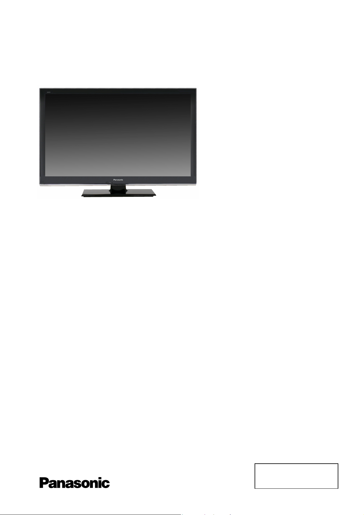
Panasonic TX-L32EM5E Schematic
ORDER No. PCZ1208127CE
Service Manual
LCD Television
TX-L32EM5E
KM19E Chassis
Specifications
Power Source: 220-240V AC, 50 / 60Hz
Rated Power Consumption: 66W
Stand-by Power Consumption: 0.30W
Aerial Impedance: 75 unbalanced, Coaxial Type
Receiving System:
DVB-T Digital terrestrial services (
DVB-C Digital cable services (
PAL I/H, B/G,
SECAM B/G, L/L’
VHF E2-E12 VHF H1-H2 ( ITALY )
VHF A-H ( ITALY ) UHF E21-E69
CATV (S01-S05) CATV S1-S10(M1-M10)
CATV S11-S20 (U1-U10) CATV S21-S41 (HYPERBAND)
PAL D/K,
SECAM D/K
VHF R1-R2 VHF R3-R5
VHF R6-R12 UHF E21-E69
PAL 525/60 (AV only)
M.NTSC (AV only)
NTSC (AV only)
Aerial Input: VHF / UHF
Operating Conditions: Temperature: 0°C 35°C
Humidity: 20% 80% RH (non condensing)
MPEG2 and MPEG4-AVC(H.264))
MPEG2 and MPEG4-AVC(H.264))
© Panasonic Corporation 2012.
Unauthorized copying
distribution is a violation of law.
and

Terminals:
2
AV1 IN Video (21 pin) 1.0V p-p 75
Audio (21 pin) 500mV rms 10k
RGB (21 pin) 0.7V p-p 75
AV1 OUT Video (21 pin) 1.0V p-p 75
Audio (21 pin) 500mV rms 1k
AV2 IN Video (RCAx1) 1V p-p 75
(COMPONENT/VIDEO) Audio (RCAx2) 500mV rms 10k
Video (RCAx3) Y:1V p-p 75 (including synchronization)
Pb, Pr: ±0.35V p-p 75
HDMI 1 / 2 Type A Connector
HDMI2: Audio Return Channel
CARD SLOT Common Interface slot (complies with CI Plus) 1
DIGITAL AUDIO OUT PCM / Dolby Digital/ Fibre optic
USB USB2.0 DC 5 V, Max. 500mA
LCD screen: L5EDDYY00413
1920 x 1080 , 16:9
Visible Diagonal 800mm
Audio Output: 10W (2x5W)
Headphones: 3.5mm (M3) stereo mini jack 1
Accessories supplied : Remote Control
2 x R6 (UM3) Batteries
Dimensions:
Width: Height: Depth:
Including TV stand 764mm 518mm 196mm
TV set only 764mm 473mm 60mm
Mass:
Including TV stand 9 0 kg
TV set only 8.0 kg
Design and Specifications are subject to change without notice. Mass and dimensions shown are approximate.
This equipment complies with the EMC standards listed below:
EN55013, EN61000-3-2, EN61000-3-3, EN55020
Warning
This service information is designed for experienced repair technicians only and is not designed for use by the general public. It does not
contain warnings or cautions to advise non-technical individuals of potencial dangers in attempting to service a product. Products
powered by electricity should be serviced or repaired only by experienced professional technicians. Any attempt to service or repair the
product or products deal within this service information by anyone else could result in serious injury or death.

CONTENTS
3
SAFETY PRECAUTIONS .......................................................................... 4
GENERAL GUIDE LINES..................................................................... 4
TOUCH – CURRENT CHECK.............................................................. 4
PREVENTION OF ELECTROSTATIC DISCHARGE (ESD)
TO ELECTROSTATICALLY SENSITIVE (ES) DEVICES .......................... 5
ABOUT LEAD FREE SOLDER (PBF)........................................................ 6
SUGGESTED PB FREE SOLDER....................................................... 6
APPLICABLE SIGNALS............................................................................. 7
SERVICE HINTS ....................................................................................... 8
CHASSIS BOARD LAYOUT ...................................................................... 9
LOCATION OF LEAD WIRING…………………………………………….9
TECHNICAL DESCRIPTION, MODEL AND KYES...................................10
SETTING INSPECTION........................................................................... 11
SELF-CHECK .......................................................................................... 12
POWER LED BLINKING TIMING CHART ............................................... 13
SERVICE MODE FUNCTION .................................................................. 14
SERVICE ................................................................................................ 15
ADJUSTMENT METHOD ........................................................................ 16
WIRING DIAGRAM.................................................................................. 17
BLOCK DIAGRAMS................................................................................. 18
PARTS LOCATION.................................................................................. 20
REPLACEMENT PARTS LIST................................................................. 22
SCHEMATIC DIAGRAMS........................................................................ 29
A-BOARD (1 OF 14) SCHEMATIC DIAGRAM ................................... 30
P-BOARD (1 OF 2) SCHEMATIC DIAGRAM...................................... 44
K-BOARD SCHEMATIC DIAGRAM ................................................... 46
CONDUCTOR VIEWS ............................................................................. 47
Safety Precautions
4
General Guide Lines
1. When servicing, observe the original lead dress. If a short circuit is found, replace all parts which have been overheated
or damaged by the short circuit.
2. After servicing, see to it that all the protective devices such as insulation barriers, insulation papers shields are properly
installed.
3. After servicing, make the following touch current checks to prevent the customer from being exposed to shock hazards.
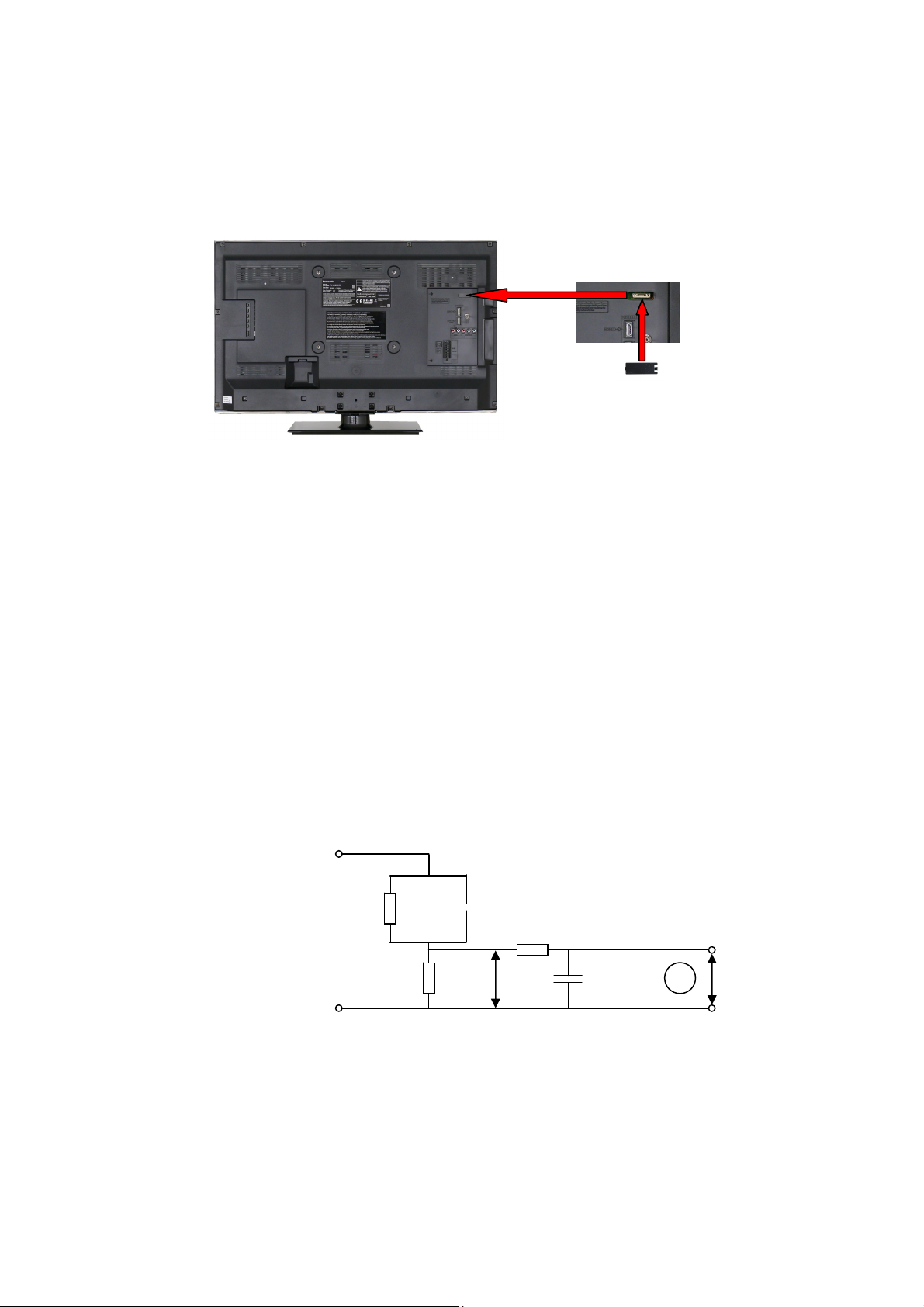
4. Always ensure cover label TKP0E16001 is correctly replaced before returning to customer (see Fig.1).
Fig. 1
Touch-Current Check
1. Plug the AC cord directly into the AC outlet. Do not use an isolation transformer for this check.
2. Connect a measuring network for touch currents between each exposed metallic part on the set and a good earth
ground such as a water pipe, as shown in Fig. 2.
3. Use Leakage Current Tester (Simpson 228 or equivalent) to measure the potential across the measuring network.
4. Check each exposed metallic part, and me asure the voltage at each point.
5. Reserve the AC plug in the AC outlet and re peat each of the above measure.
6. The potential at any point (TOUCH CURRENT) expressed as voltage U1 and U2, does not exceed the following values:
For a. c.: U1 = 35 V (peak) and U2 = 0.35 V (peak);
For d. c.: U1 = 1.0 V,
Note:
The limit value of U2 = 0.35 V (peak) for a. c. and U1 = 1.0 V for d. c. correspond to the values 0.7 mA (peak) a. c. and
2.0 mA d. c.
The limit value U1 = 35 V (peak) for a. c. correspond to the value 70 mA (peak) a. c. for frequencies greater than 100
kHz.
7. In case a measurement is out of the limits specified, there is a possibility of a shock hazard, and the equipment should
be repaired and rechecked before it is returned to the customer.
COLD
WATER PIPE
(EARTH GROUND)
TO
APPLIANCES
EXPOSED
METAL PARTS
Resistance values in ohms ()
V: Voltmetr or oscilloscope
(r.m.s. or peak reading)
NOTE – Appropriate measures should be taken to obtain the correct value in case of non-sinusoidal waveforms
Measuring network for TOUCH CURRENTS
C
=1500
R
S
R0=500
Input resistance: 1M
Input capacitance:200pF
Frequency range: 15Hz to 1MHz and d.c.respectively
Fig. 2
=0.22F
S
U
10k
(V)
1
0.022F
V
U2 (V)

Prevention of Electrostatic Discharge (ESD) to Electrostatically
5
Sensitive (ES) Devices
Some semiconductor (solid state) devices can be damaged easily by static electricity. Such components commonly are
called Electrostatically Sensitive (ES) Devices. Examples of typical ES devices are integrated circuits and some field-effect
transistors and semiconductor "chip" components. The following techniques should be used to help reduce the incidence of
component damage caused by electrostatic discharge (ESD).
1. Immediately before handling any semiconductor component or semiconductor-equipped assembly, drain off any ESD on
your body by touching a known earth ground. Alternatively, obtain and wear a commercially available discharging ESD
wrist strap, which should be removed for potential shock reasons prior to applying power to the unit under test.
2. After removing an electrical assembly equipped with ES devices, place the assembly on a conductive surface such as
aluminum foil, to prevent electrostatic charge build up or exposure of the assembly.
3. Use only a grounded-tip soldering iron to solder or unsolder ES devices.
4. Use only an anti-static solder removal device. Some solder removal devices not classified as "anti-static (ESD
protected)" can generate electrical charge sufficient to damage ES devices.
5. Do not use freon-propelled chemicals. These can generate electrical charges sufficient to damage ES devices.
6. Do not remove a replacement ES device from its protective package until immediately before you are ready to install it.
(Most replacement ES devices are packaged with leads electrically shorted together by conductive foam, aluminum foil
or comparable conductive material).
7. Immediately before removing the protective material from the leads of a replacement ES device, touch the protective
material to the chassis or circuit assembly into which the device will be installed.
Caution
Be sure no power is applied to the chassis or circuit, and observe all other safety precautions.
8. Minimize bodily motions when handling unpackaged replacement ES devices. (Otherwise harmless motion such as the
brushing together of your clothes fabric or the lifting of your foot from a carpeted floor can generate static electricity
(ESD) sufficient to damage an ES device).
There are special components used in this equipment which are important for safety.
These parts are marked by in schematic diagrams, exploded views and replacement parts list. It is essential that
these critical parts should be replaced with manufacturer’s specified parts to prevent shock, fire, or other hazards. Do
not modify the original design without permission of manufacturer.
IMPORTANT SAFETY NOTICE
About lead free solder (PbF)
6
Note: Lead is listed as (Pb) in the periodic table of elements.
In the information below, Pb will refer to Lead solder, and PbF will refer to Lead Free Solder.
The Lead Free Solder used in our manufacturing process and discussed below is (Sn+Ag+Cu).
That is Tin (Sn), Silver (Ag) and Copper (Cu) although other types are available.
This model uses Pb Free solder in it’s manufacture due to environmental conservation issues. For service and repair work,
we’d suggest the use of Pb free solder as well, although Pb solder may be used.
PCBs manufactured using lead free solder will have the PbF within a leaf Symbol
stamped on the back of PCB.
Caution
Pb free solder has a higher melting point than standard solder. Typically the melting point is 50 ~ 70 °F (30~40°C)
higher. Please use a high temperature soldering iron and set it to 700 ± 20 °F (370 ± 10 °C).
Pb free solder will tend to splash when heated too high (about 1100 °F or 600 °C).
If you must use Pb solder, please completely remove all of the Pb free solder on the pins or solder area before
applying Pb solder. If this is not practical, be sure to heat the Pb free solder until it melts, before applying Pb solder.
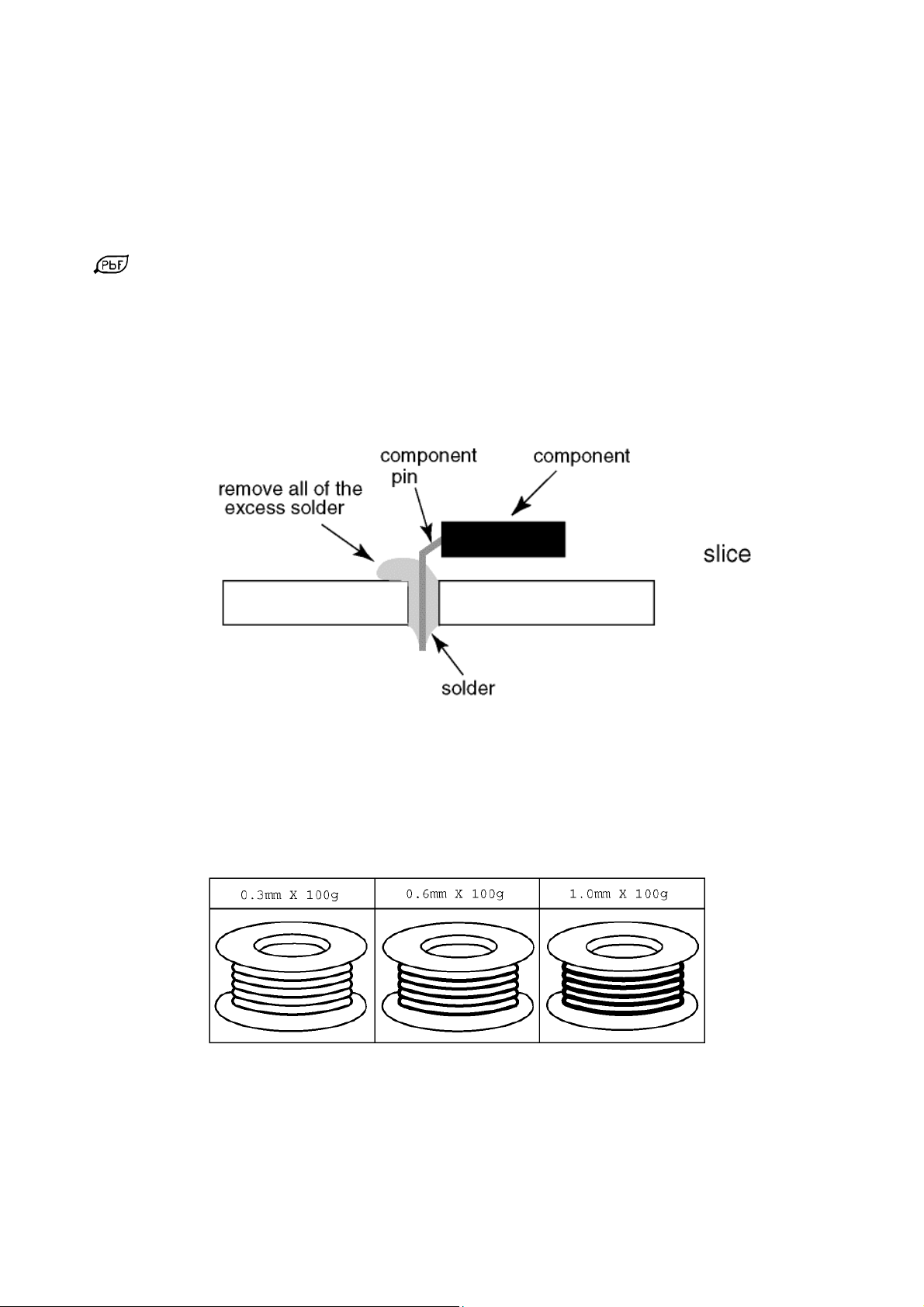
After applying PbF solder to double layered boards, please check the component side for excess solder which may
flow onto the opposite side. (see Fig.3)
Suggested Pb free solder
There are several kinds of Pb free solder available for purchase. This product uses Sn+Ag+Cu (tin, silver, copper) solder.
However, Sn+Cu (tin, copper), Sn+Zn+Bi (tin, zinc, bismuth) solder can also be used. (see Fig.4)
Fig.3
Fig.4
Applicable Signals
7
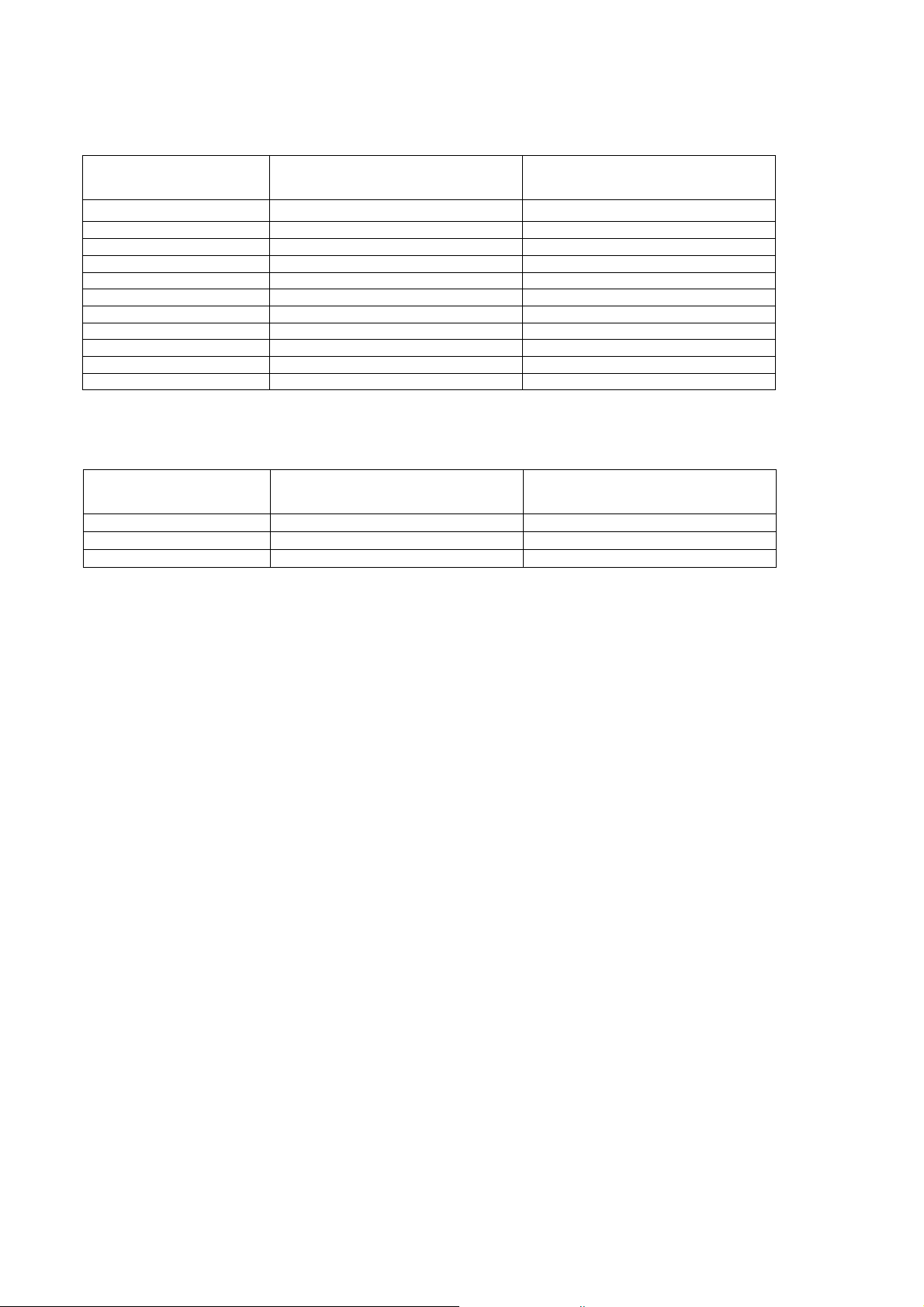
Component (Y, Pb, Pr), HDMI
Applicable input signal for PC is basically compatible to HDMI standard timing.
Signal name COMPONENT HDMI
525 (480) / 60i * *
525 (480) / 60p * *
625 (576) / 50i * *
625 (576) / 50p * *
750 (720) / 60p * *
750 (720) / 50p * *
1,125 (1,080) / 60i * *
1,125 (1,080) / 50i * *
1,125 (1,080) / 60p *
1,125 (1,080) / 50p *
1,125 (1,080) / 24p *
PC (from HDMI terminal)
Signal name Horizontal frequency (kHz) Vertical frequency (Hz)
640 480 @60 Hz
1,280 720 @60Hz
1,920 1,080 @60Hz
Note:
Signals other than above may not be displayed properly.
The above signals are reformatted for optimal viewing on your display.
PC signal is magnified or compressed for display, so that it may not be possible to show fine detail
with sufficient clarity.
31.47 60.00
45.00 60.00
67.50 60.00
Service Hints
8
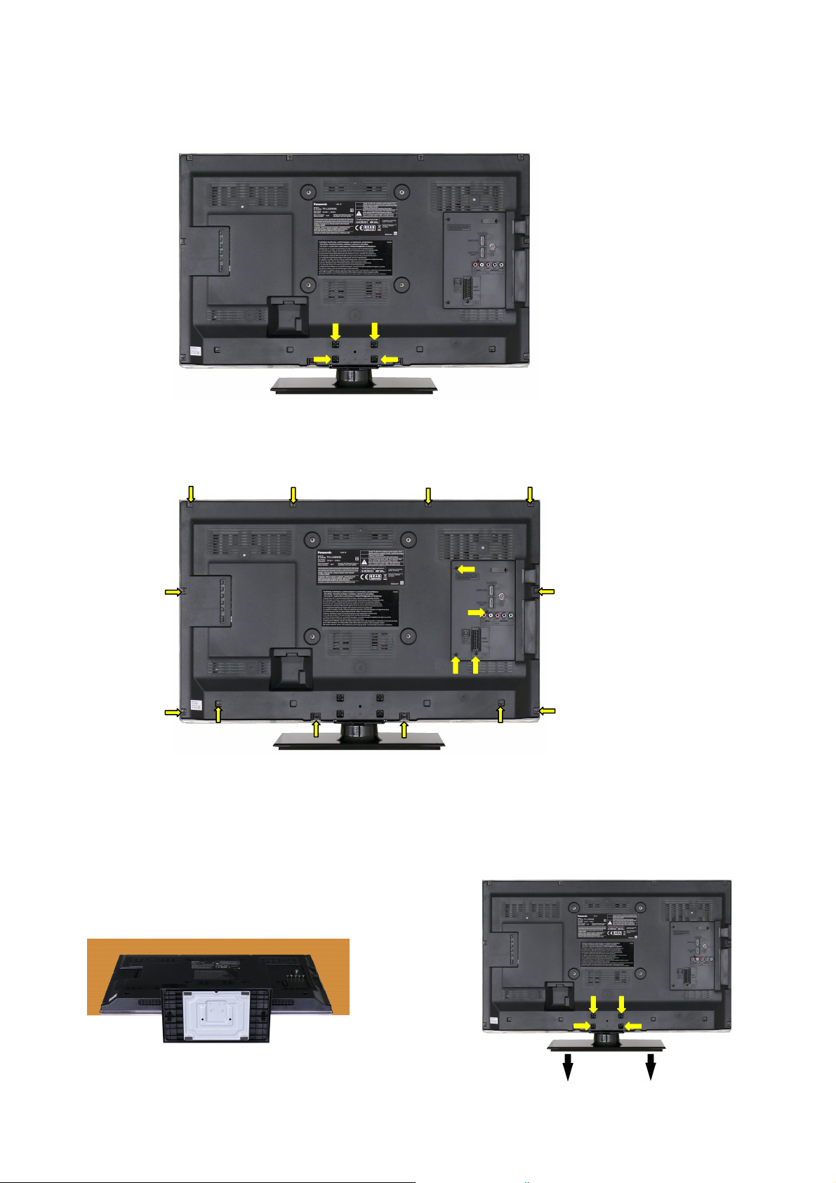
How to remove the backcover
Remove the 4 fixing screws (see Fig.5)
(4)
(4)
SCREWS
(4) XYN4+F12FJK /4pcs/
Remove the 16 fixing screws and the backcover. (see Fig.6)
(1)
(1)
(4)
Fig.5
(1)
(4)
(1)
(1)
Fig.6
(1)
(2)
(2)
(2)
(2)
(1)(1)
(1)
SCREWS
(1) THTD030J /12pcs
(2) XTV3+12JFJK /4pcs
(1)
(1)
(1)
How to remove the pedestal assembly.
Lay the main unit face down. (see Fig.7)
Remove the 4 fixing screws and the pedestal assembly. (see Fig.8)
Fig.7
(4)
(4)
(4)
Fig.8
(4)
Chassis Board Layout
A
A
A10A
9
P-BOARD
K-BOARD
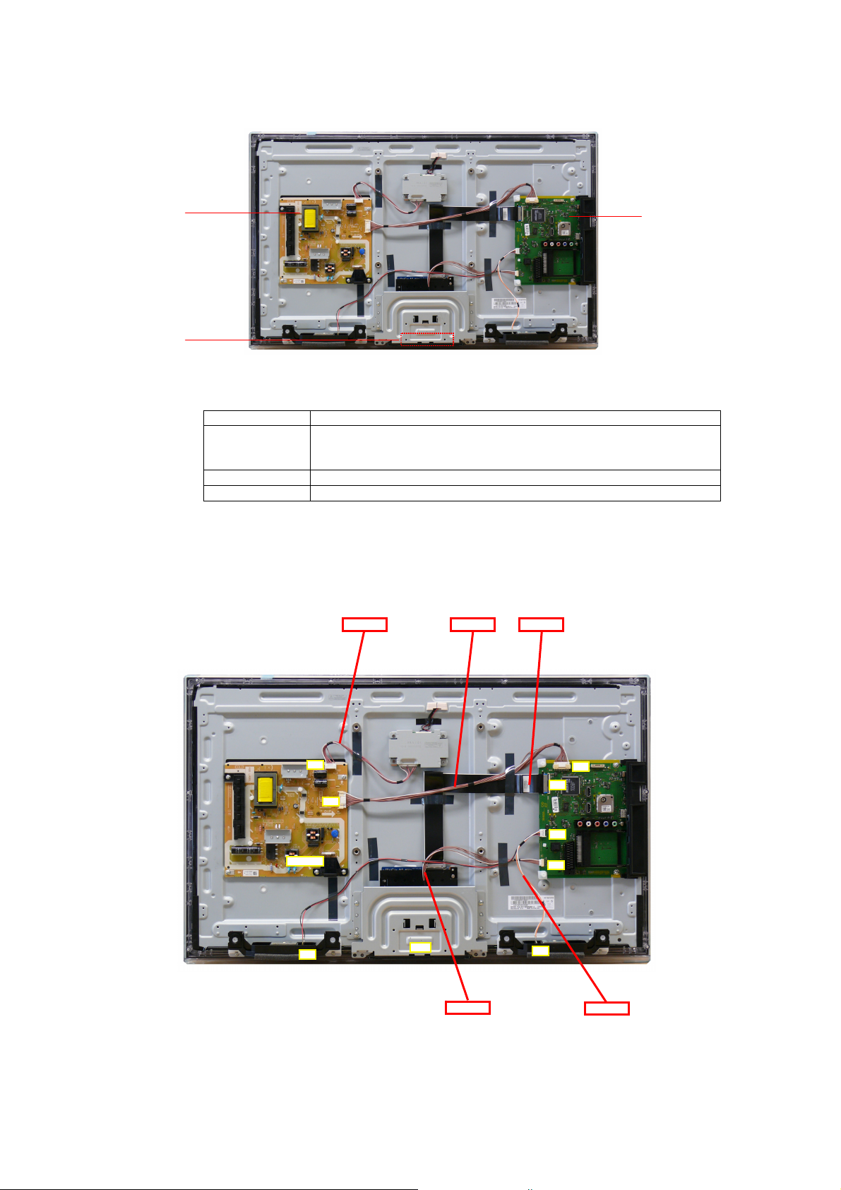
Board Name Function
AV Terminal, HDMI, Digital Audio Out,TV tuner, CI slot,
A-Board
P-Board Power Supply, Main Input, Key button, LED Driver
K-Board Remote Receiver, R/G LED, C.A.T.S.
MicroProcessor IC8001, Speaker Out, EEPROM,
Flash Memory, DDR SDRAM, USB
Location of Lead Wiring
To find the Part Number of required wire in Replacement Parts List click on the wire name in red box.
LD-P3
A09-P2
A16-CN
A-BOARD
P3
P2
09
16
JK7101
12
SP
K10
SP
A10-K10
A12-SP

Technical Description
10
Model and Keys:
All KEYS are not generated for all models.
The necessary KEYS are only generated and stored depend on the feature of models.
Model No.
TX-L32EM5E Yes Yes
CI PLUS HDCP
Keys

Setting Inspection
11
Voltage Confirmation
A board
Description Test point Voltage
SUB 1.8 V TP8700 1.74V - 1.9V
SUB1.2V TP8000 1.14V – 1.26V
SUB3.3V TP8701 3.19V - 3.46V
SUB5V TP8702 4.9V – 5.1V
STB5V TP5400 4.9V - 5.1V
PNL12V TP8307 11.5V – 12.5V
P board
Description Test point *Voltage( STEP1 ) **Voltage ( STEP2 )
24V TP7509 <1V 24V±1.2V
16.4V TP7508 <1V 16.4V±0.8V
5.3VS TP7507 5.3V±0.1V 5.3V±0.1V
STEP1 : Connect AC 230V to JK7101
STEP2 : Connect DC 2,5V to TV_SUB_ON P2 connector - pin 6 (TP7506) from voltage divider.

Self Check
V
12
Self-check is used to automatically check the bus lines and hexadecimal code of the TV set. To enter Self-Check mode, keep
pressing the down (-/v) button on the TV set and press the
the TV set at the power button.
TX-L32EM5E
32HD
TUN O.K.
MEM O.K.
ID O.K
Panasonic 2012 LCD
Self Check Complete
SOFT
EEP 1.00.000a
Model id 09222100000004
Display Ref. No. Description P.C.B.
TUN TU4802 TUNER A-Board
MEM IC8007 EEPROM A-Board
ID IC8001 MICRO PROCESSOR A-Board
MENU button on the remote control. To exit Self Check, switch off
er.2010
If the CCU ports have been checked and found to be incorrect or not located then " - - " will appear in place of "O.K.".
Power LED blinking timing chart
13
1. Subject
Information of LED Flashing timing chart.
2. Contents
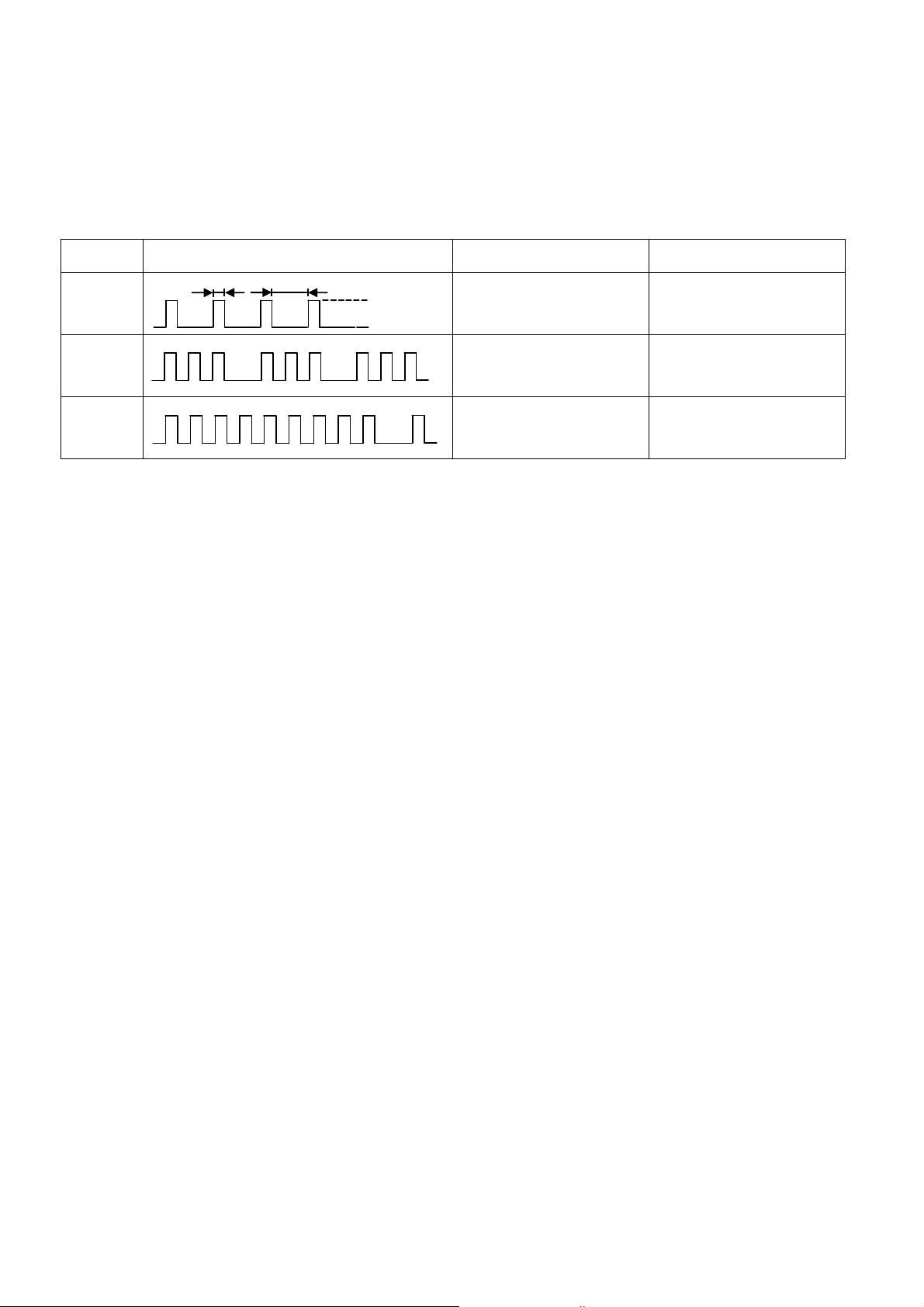
When abnormality has occurred the unit, the protection circuit operates and reset to the stand by mode. At this time, the
defective block can be identified by number of blinking of the Power LED on the front panel of the unit.
Blinking
times
Once
1 BL_SOS
3 POWER SOS
Blinking timing Contents Check point
4 sec
Light
No Light
A BOARD
A BOARD
P BOARD
9 SOUND_SOS
A BOARD

Service Mode Function
14
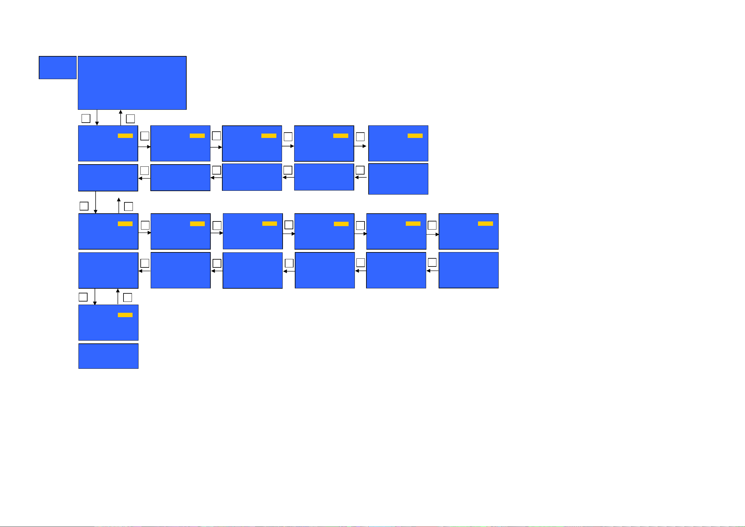
MPU controls the functions switching for each IICs through IIC bus in this chassis. The following setting and adjustment can be
adjusted by remote control in Service Menu
How to enter SERVICE
While pressing (-/v) button on TV unit, press on the remote
control for 3 times within 2 seconds.
Note:
To exit from Service mode, press the exit button on remote control.
0
Service
A
A
V
15
SERVICE
ADJUST
WB-ADJ
OPTION
SOFT V2.010 MODEL ID 09222100000004
EEP 01.00.000a INV Cnt 0
TIME 0:0 COUNT 0
PCTCP 00.00.00.00.00
1 2
ADJUST DYNAMIC
H-POS
1,2:MAIN SELECT
3,4:SUB SELECT
9:PICTURE MENU SELECT
VOL :ADJUST
OK :WRITE
0
ADJUST DYNAMIC
H-AMP
3
1,2:MAIN SELECT
4
3,4:SUB SELECT
9:PICTURE MENU SELECT
VOL :ADJUST
OK :WRITE
1 2
WB-ADJ DYNAMIC
R-GAIN
BEFORE FF
COLOR TEMP NORMAL
1,2:MAIN SELECT
3,4:SUB SELECT
7:COLOR TEMP SELECT
9:PICTURE MENU SELECT
0:WB METHOD SELECT
VOL :ADJUST
OK :WRITE/WB DIFF ADJ
FF
WB-ADJ DYNAMIC
G-GAIN
3
BEFORE C7
COLOR TEMP NORMAL
1,2:MAIN SELECT
3,4:SUB SELECT
4
7:COLOR TEMP SELECT
9:PICTURE MENU SELECT
0:WB METHOD SELECT
VOL :ADJUST
OK :WRITE/WB DIFF ADJ
1 2
OPTION DYNAMIC
BootLoader
upgrade
1,2:MAIN SELECT
VOL:ADJUST
OK:WRITE
No
C7
Key Command
Press the 3/4 button to change the adjustment values or function.
Press the 1/2 button to step up/down through the functions and adjustments
Press the numerical button VOLUME (+/-) to change of each option item.
Press the OK button after each adjustment has been made to store the required values.
0
1,2:MAIN SELECT
4
3,4:SUB SELECT
9:PICTURE MENU SELECT
VOL :ADJUST
OK :WRITE
WB-ADJ DYNAMIC
B-GAIN
3
BEFORE F8
COLOR TEMP NORMAL
1,2:MAIN SELECT
3,4:SUB SELECT
4
7:COLOR TEMP SELECT
9:PICTURE MENU SELECT
0:WB METHOD SELECT
VOL :ADJUST
OK :WRITE/WB DIFF ADJ
0
F8
DJUST DYNAMIC
V-POS
3
ADJUST DYNAMIC
V-AMP
3
1,2:MAIN SELECT
4
3,4:SUB SELECT
9:PICTURE MENU SELECT
VOL :ADJUST
OK :WRITE
WB-ADJ DYNAMIC
R-CENT
3
BEFORE 94
COLOR TEMP NORMAL
1,2:MAIN SELECT
3,4:SUB SELECT
4
7:COLOR TEMP SELECT
9:PICTURE MENU SELECT
0:WB METHOD SELECT
VOL :ADJUST
OK :WRITE/WB DIFF ADJ
0
94
DJUST DYNAMIC
VCOM
3
BEFORE 197
1,2:MAIN SELECT
4
3,4:SUB SELECT
5 :FLICKER PATTERN
9 :PICTURE MENU SELECT
OK :WRITE
OL :ADJUST
WB-ADJ DYNAMIC
G-CENT
3
BEFORE 80
COLOR TEMP NORMAL
1,2:MAIN SELECT
3,4:SUB SELECT
4
7:COLOR TEMP SELECT
9:PICTURE MENU SELECT
0:WB METHOD SELECT
VOL :ADJUST
OK :WRITE/WB DIFF ADJ
197
80
WB-ADJ DYNAMIC
B-CENT
3
BEFORE 9B
COLOR TEMP NORMAL
1,2:MAIN SELECT
3,4:SUB SELECT
4
7:COLOR TEMP SELECT
9:PICTURE MENU SELECT
0:WB METHOD SELECT
VOL :ADJUST
OK :WRITE/WB DIFF ADJ
9B

Adjustment Method
16
White Balance Adjustment
Instrument Name Connect to Remarks
1. Remote controller
2. LCD WB meter (Minolta CS-1000A e qu ivalent)
3. Comunication jig
4. Computer for external control
Procedure Remarks
White Balance adjustment
1. Procedure basically performs checking using the production software and
make automatic adjustment using external computer.
2. It adjusts in the mode of : Colour balance Cool
Viewing Mode Dynamic
WHITE Normal
x: 0.270 ± 0.010
y: 0.276 ± 0.010
GRAY Normal
x: 0.270 ± 0.010
y: 0.278 ± 0.010
Correlation can be also taken by
CA-210 or equivalent
Let the panel standfor more than 3
hours at more than 20 °C.
Basically perform adjustment in the
ambient environment of room
temperature more than 20 °C.
The aging time is more than 20 min
at above room temperature.
100% WHITE
50% GRAY
 Loading...