

Page 1
MODELO :
SC-TM22
SB-TM22
$03/,),&$'25 6$70
3RWHQFLDGHVDOLGD :3032
&RQVXPRGHSRWHQFLD :
$OLPHQWDFLyQ 9FD+]
6HQVLELOLGDG$8; P9
5DQJRGHVLQWRQtD$0 N+]SDVRGHN+]
5DQJRGHVLQWRQtD)0 0+]SDVRGH.+]
'LPHQVLRQHVE[K[O PP[PP[PP
3HVR .JDSUR[
%DIOHV 6%70
,PSHGDQFLDGHHQWUDGD 7
%RFLQD7ZHHWHU FP
%RFLQD:RRIHU FP
'LPHQVLRQHVE[K[O
3HVR .JDSUR[
SA-TM22
0+]SDVRGH.+]
PP[PP[PP
SB-TM22
3RWHQFLDGHVDOLGDDPSOLILFDGRU
6&70
:5&0SRUFDQDO:N+]'$7
Page 2
1 Safety Precaution
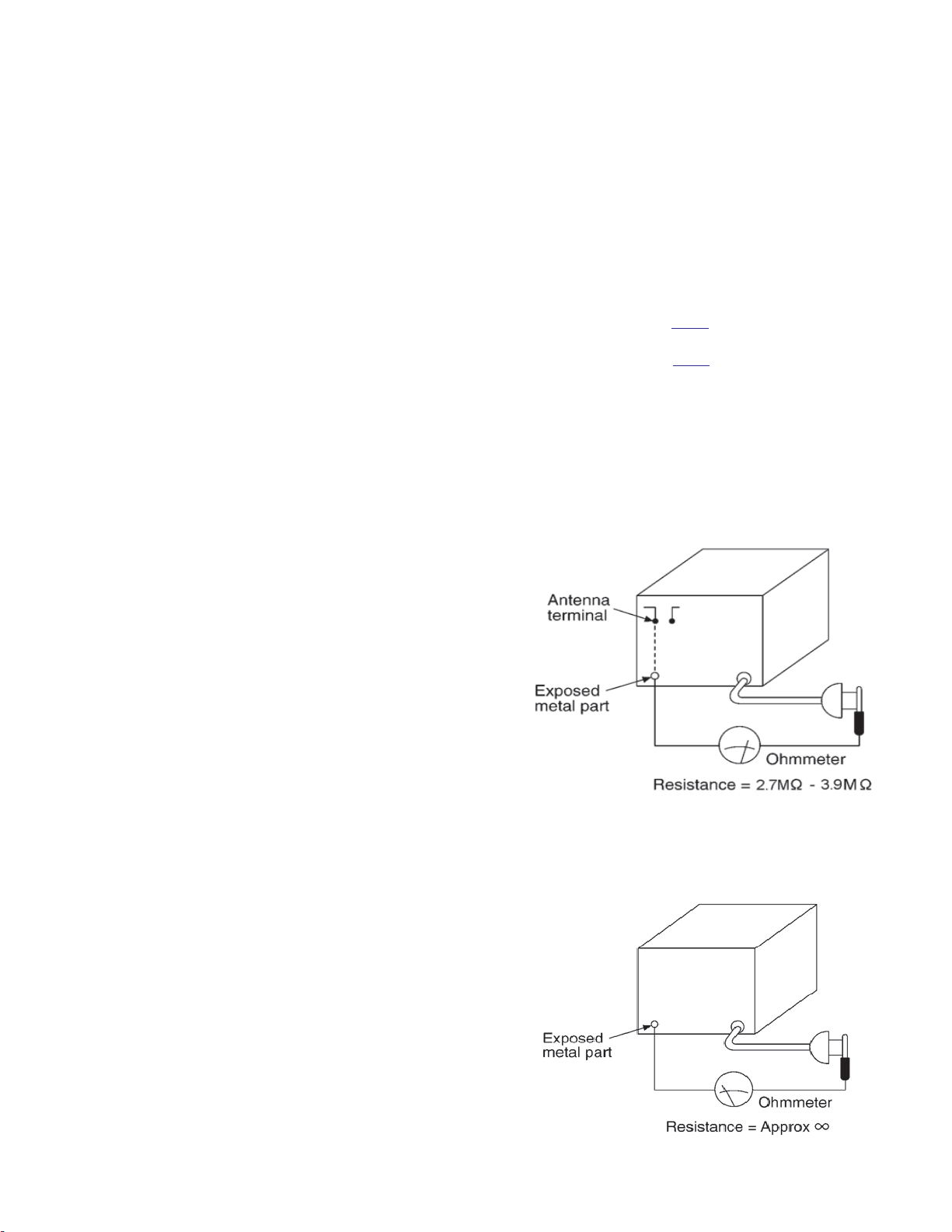
1.1 Insulation Resistance Test
(This “Safety Precaution” is applied only in U.S.A.)
Before servicing, unplug the power cord to prevent an electric
shock.
When replacing parts, use only manufacturer’s recommended
components for safety.
Check the condition of the power cord. Replace if wear or
damage is evident.
After servicing, be sure to restore the lead dress, insulation
barriers, insulation papers, shields, etc.
Before returning the serviced equipment to the customer, be
sure to make the following insulation resistance test to
prevent the customer from being exposed to a shock
hazard.
Unplug the power cord and short the two prongs of the plug
with a jumper wire.
Turn on the power switch.
Measure the resistance value with ohmmeter between the jumper
AC plug and each exposed metal cabinet part, such as
screwheads, antenna, control shafts, handle brackets, etc.Measure
the resistance value with ohmmeter between the jumper AC
plugand each exposed metal cabinet part, such as screwheads,
antenna, control shafts, handle brackets, etc.
Equipment with antenna terminals should read between 2.7M and
3.9M to all exposed parts*. ( Fig.1 )
Equipment without antenna terminals should read approximately
infinity to all exposed parts. ( Fig.2 )
*Note : Some exposed parts may be isolated from the chassisby
design. These will read infinity.
If the measurement is outside the specified limits, there is a
possibility of a shock hazard. The equipment should be
repaired and re-checked before it is returned to the
customer.
Fig.1
Fig.2
Page 3

2 Before Repair and
4 Prevention of Electr o
Adjustment
Disconnect AC power, discharge Power Supply Capacitors C520
and C540 through a 10˜, 5W resistor to ground.
DO NOT SHORT-CIRCUIT DIRECTLY (with a screwdriver
blade, for instance), as this may destroy solid state devices.
After repairs are completed, restore power gradually using a
variac, to avoid overcurrent.
Current consumption at AC 120V, 60 Hz in NO SIGNAL mode
(volume min at CD mode) should be ~600mA.
3 Protection Cir cuitry
The protection circuitry may have operated if either of the
following conditions are noticed:
• No sound is heard when the power is turned on.
• Sound stops during a performance.
The function of this circuitry is to prevent circuitry damage if, for
example, the positive and negative speaker connection wires are
“shorted”, or if speaker systems with an impedance less than the
indicated rated impedance of the amplifier are used.
If this occurs, follow the procedure outlines below:
Turn off the power.
Static Discharge (ESD) to
Electrostatically Sensitive
(ES) Devices
Some semiconductor (solid state) devices can be damaged easily
by electricity. Such components commonly are called
Electrostatically Sensitive (ES) Devices. Examples of typical ES
devices are integrated circuits and some field-effect transistorsand
semiconductor “chip” components. The following techniques
should be used to help reduce the incidence of component damage
caused by electro static discharge (ESD).
Immediately before handling any semiconductor component
or semiconductor-equiped assembly, drain off any ESD
on your body by touching a known earth ground.
Alternatively, obtain and wear a commercially available
discharging ESD wrist strap, whichshould be removed
for potential shock reasons prior to applying power to the
unit under test.
After removing an electrical assembly equiped with ES
devices, place the assembly on a conductive surface such
as aluminium foil, to prevent electrostatic charge build up
or exposure of the assembly.
Use only a grounded-tip soldering iron to solder or unsolder
ES devices.
Use only an anti-static solder remover device. Some solder
removal devices not classified as “anti-static (ESD
protected)” can generate electrical charge to damage ES
devices.
Determine the cause of the problem and correct it.
Turn on the power once again after one minute.
Note :
When the protection circuitry functions, the unit will not operate
unless the power is first turned off and then on again.
Do not use freon-propelled chemicals. These can generate
electrical charges sufficient to damage ES devices.
Do not remove a replacement ES device from its protective
package until immediately before you are ready to install
it. (Most replacement ES devices are packaged with leads
electrically shorted together by conductive foam,
aluminium foil orcomparable conductive material).
Immediately before removing the protective material from the
leads of a replacement ES device, touch the protective material to
the chassis or circuit assembly into which the device will be
installed.
Page 4
Caution
Be sure no power is applied to the chassis or circuit, and observe all other safety precautions. Minimize body motions
when handling unpackaged replacement ES devices. (Otherwise harmless motion such as the brushing together of your
clothes fabric or the lifting of your foot from a carpeted floor can generate static electricity (ESD) sufficient todamage an
ES device).
5 Handling the Lead-free
Solder
5.1 About lead free solder (PbF)
Distinction of PbF P.C.B.:
P.C.B.s (manufactured) using lead free solder will have a PbF
stamp on the P.C.B.
Caution:
• Pb free solder has a higher melting point than standard
solder; Typically the melting point is 50 - 70°F (30 - 40°C) higher.
Please use a high temperature soldering iron. In case of soldering
iron with temperature control,please set it to 700 ± 20°F (370 ±
10°C).
• Pb free solder will tend to splash when heated too high
(about 1100°F/600°C).
• When soldering or unsoldering, please completely
remove all of the solder on the pins or solder area, and be sure to
heat the soldering points with the Pb free solder until it melts
enough.
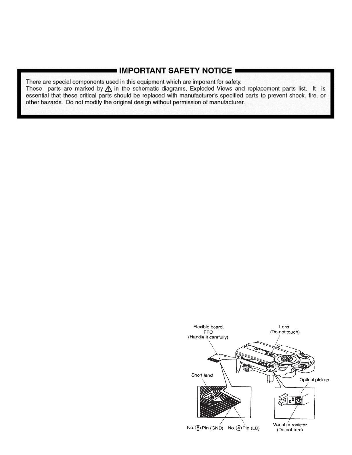
6 Handling Precautions For
Traverse Deck
The laser diode in the traverse deck (optical pickup) may break
down due to potential difference caused by static electricity of
clothes or human body.
So, be careful of electrostatic breakdown during repair of the
traverse deck (optical pickup).
• Handling of traverse deck (optical pickup)
Do not subject the traverse deck (optical pickup) to static
electricity as it is extremely sensitive to electrical shock.
The short land between the No.4(LD) and No.5(GND) pins on
the flexible board (FFC) is shorted with a solder build-up
to prevent damage to the laser diode.To connect to the PC
board, be sure to open by removing the solder build-up,
and finishthe workquickly.
Take care not to apply excessive stress to the flexible board
(FFC).
Do not turn the variable resistor (laser power adjustment). It
has already been adjusted.
Fig 6.1
Page 5

Grounding for electrostatic breakdown prevention
Human body grounding
7 Precaution of Laser
Use the anti-static wrist strap to discharge the static
electricity from your body.
Work table grounding
Put a conductive material (sheet) or steel sheet on the
area where the traverse deck (optical pickup) is placed,
and ground the sheet.
Caution :
The static electricity of your clothes will not be grounded through
the wrist strap. So, take care not to let your clothes touch the
traverse deck (optical pickup).
Caution when Replacing the Traverse Deck :
The traverse deck has a short point shorted with solder to protect
the laser diode against electroststics breakdown. Be sure to
remove the solder from the short point before making
connections.
Fig 6.2
Diode
CAUTION:
This unit utilizes a class 1 laser.
Invisible laser radiation is emitted from the optical pickup lens.
Wavelength: 780nm.
When the unit is turned on:
Do not look directly into the pick up lens.
Do not use optical instruments to look at the pick up lens.
Do not adjust the preset variable resistor on the pickup lens.
Do not disassemble the optical pick up unit.
If the optical pick up is replaced, use the manufacturer’s
specified replacement pick up only.
Use of control or adjustments or performance of procedures
other than those specified herein may result in hazardous
radiation exposure.
CAUTION!
THIS PRODUCT UTILIZES A LASER.
USE OF CONTROLS OR ADJUSTMENTS OR PERFORMANCE OF
PROCEDURES OTHER THAN THOSE SPECIFIED HEREIN MAY
RESULT IN HAZARDOUSRADIATION EXPOSURE.
Use of caution label
Page 6
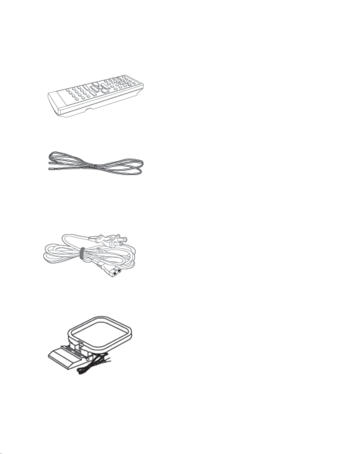
8 Accessories
Remote Control Transmitter
( EUR7710020)
FM Indoor Antenna
(N1EAYY000004)
9 Operacion procedures
( see next page )
AC Power Supply Cord
( SJA168-1A )
AM Loop Antenna
( N1DADYY00002 )
Page 7
Page 8
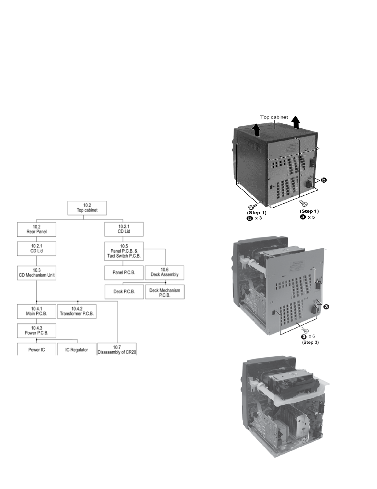
10 Disassembly and
10.2 Disassembly of Top Cabinet
Assembly of Main
Component
10.1 Disassembly flow chart
The following chart is the procedure for disassembling the casing
and inside parts for internal inspection when carrying out the
servicing.
To assemble the unit, reverse the steps shown in the chart as
below.
and Rear Panel
Step 1 Remove 3 screws on each side and 5 screws at rear panel.
Step 2 Lift up both sides of top cabinet, push the cabinet ass’y
toward the rear and remove it.
Disassembly of Rear Panel
Step 3 Remove 6 screws.
Step 4 Draw rear panel backward to remove it.
Page 9

10.2.1 Disassembly for CD Lid
(The CD changer unit can be removed after the CD Lid is
removed)
• Follow the (Step 1) - (Step 5) of Item 10.2 - Disassembly
of Top Cabinet and Rear Panel
When opening the disc tray automatically (Using Power Supply)
Step 1 Connect the AC power cord.
Step 2 Press the POWER button to power up the main unit.
Step 5 Press the OPEN/CLOSE button, the disc tray will close.
[Open the disc tray manually (Using service tools)]
Step 3 Press the OPEN/CLOSE button, the disc tray will open
automatically.
Step 1 Insert the gear tool into the hole on the underside of CD
chassis and then rotate in the direction of arrow. The disc tray will
be open.
Step 4 Release the 2 claws, and then remove the CD Lid.
Page 10
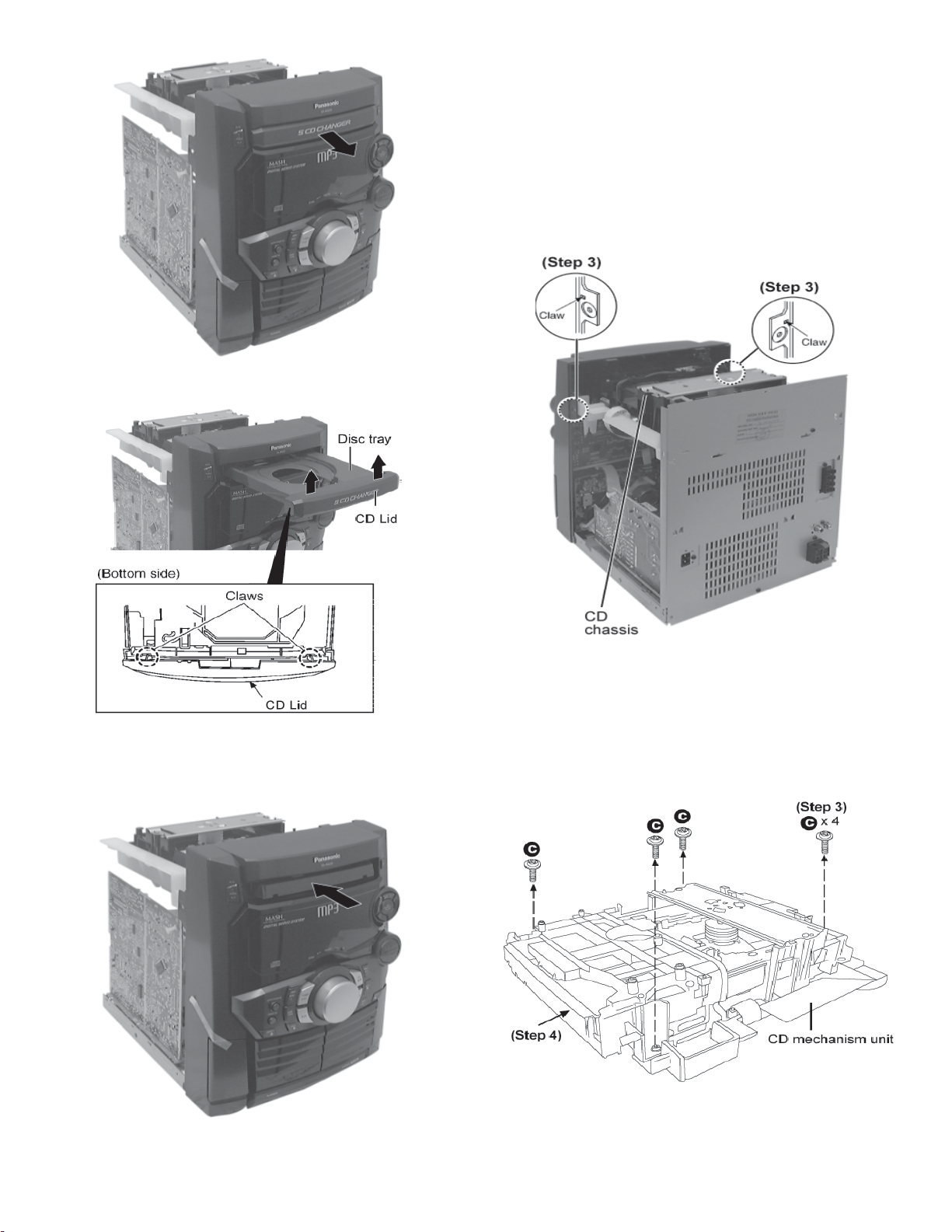
Step 2 Release the 2 claws, and then remove the CD lid cover.
10.3 Disassembly of CD Mechanism
Unit
• Follow the (Step 1) - (Step 2) of Item 10.2 - Disassembly
of Top Cabinet and Rear Panel
• Follow the (Step 1) - (Step 5) of Item 10.2.1 Disassembly for CD Lid
Step 1 Detach the FFC boards (CN309 & CN310).
Step 3 Repeat Step 2 but rotate the gear tools in anti-clockwise
direction.
Step 2 Release the claws of both ends, and then lift up the CD
Mechanism Unit.
Step 4 The disc tray will be close.
Page 11
Step 3 Remove 4 screws.
Step 4 Remove the CD chassis.
Step 5 Lay the CD mechanism unit as shown.
• Note:
For disassembly of CD mechanism unit, please refer to
Section 10.7 of this manual.
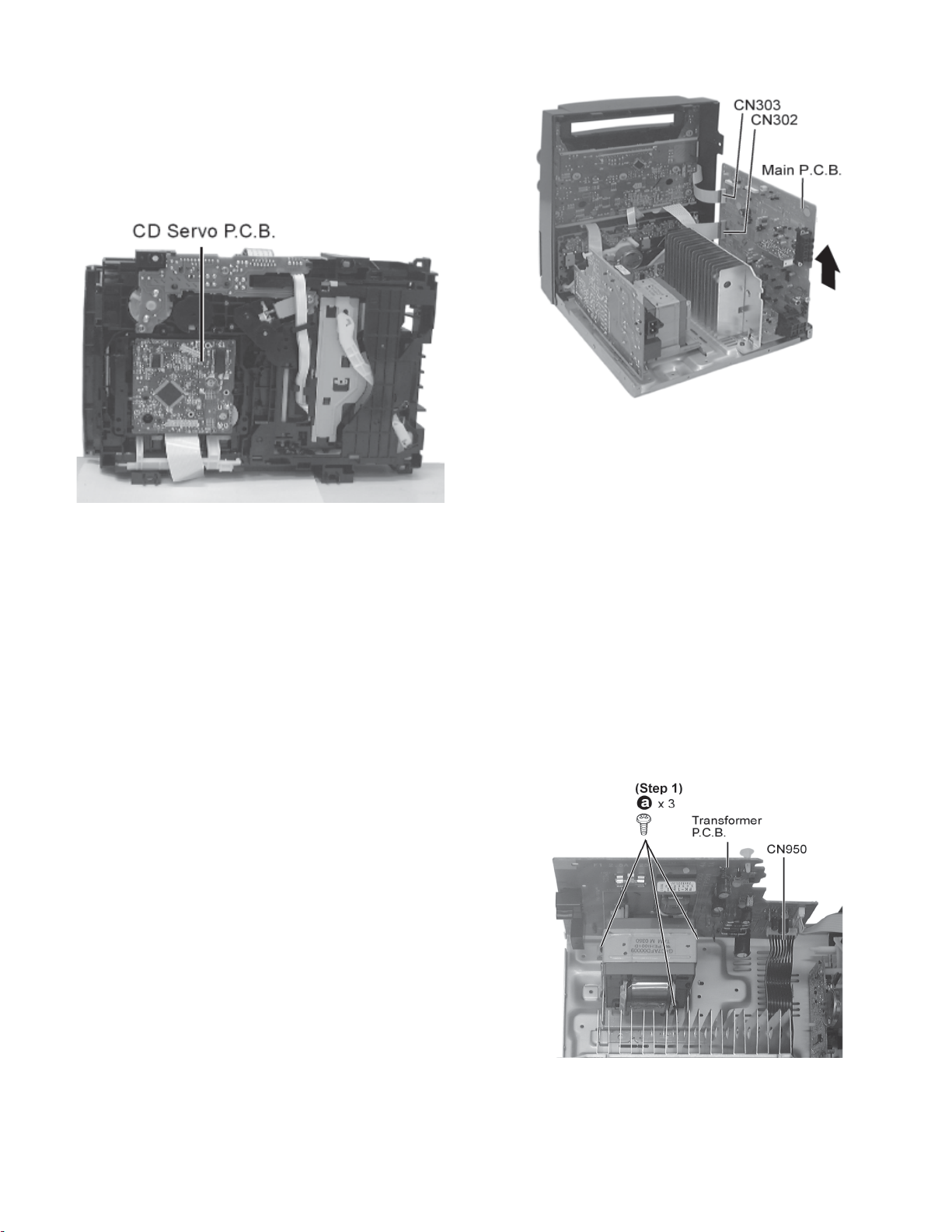
Step 2 Lift up Main P.C.B. by disconnect CN500 & CN501 as
arrow shown above.
10.4 Disassembly Main P.C.B.,
Transformer P.C.B.& Power P.C.B.
10.4.1 Disassembly for the Main
P.C.B.
• Follow the (Step 1) - (Step 4) of Item 10.2 - Disassembly
of Top Cabinet and Rear Panel
• Follow the (Step 1) - (Step 5) of Item 10.2.1 Disassembly for CD Lid
• Follow the (Step 1) - (Step 2) of Item 10.3 - Disassembly
of the CD Mechanism Unit
Step 1 Disconnect FFC boards at CN303, CN302 & CN304 .
10.4.2 Disassembly of the
Transformer P.C.B.
• Follow the (Step 1) - (Step 4) of Item 10.2 - Disassembly
of Top Cabinet and Rear Panel
• Follow the (Step 1) - (Step 5) of Item 10.2.1 Disassembly for CD Lid
• Follow the (Step 1) - (Step 2) of Item 10.3 - Disassembly
of the CD Mechanism Unit
Step 1 Remove 3 screws.
Step 2 Disconnect connector CN950.
Page 12
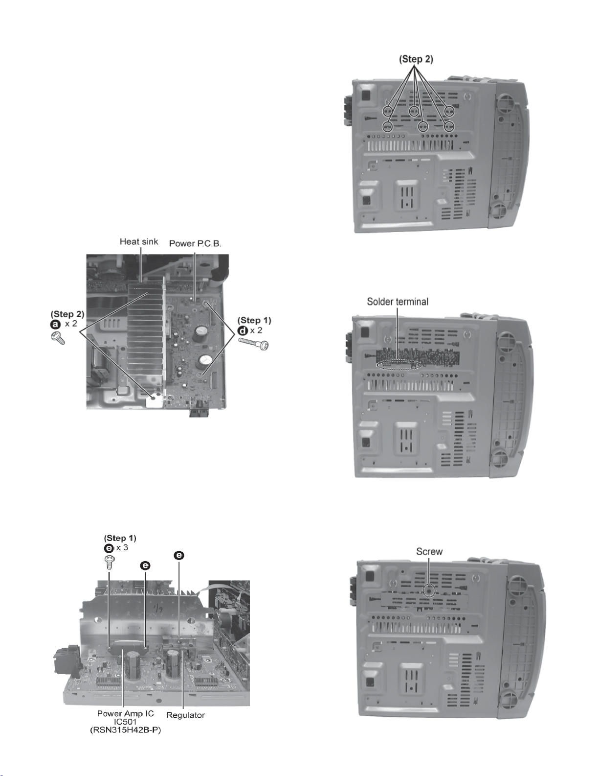
10.4.3 Disassembly of the Power
P.C.B.
• Follow the (Step 1) - (Step 4) of Item 10.2 - Disassembly
of Top Cabinet and Rear Panel
• Follow the (Step 1) - (Step 5) of Item 10.2.1 Disassembly for CD Lid
• Follow the (Step 1) - (Step 2) of Item 10.3 - Disassembly
of the CD Mechanism Unit
• Follow the (Step 1) - (Step 2) of Item 10.4.1 Disassembly for the Main P.C.B.
Step 1 Remove 2 screws.
Step 2 Remove the 2 screws fixed at heat sink.
Step 2 Break the joint with a metal cutter as shown below.
Step 3 Unsolder the terminals of Power Amp IC, transistor and
replace the components.
NOTE:
Insulate Power P.C.B. with insulation material to avoid short
circuit.
• Replacement of Power Amplifier IC & Voltage Regulator
Step 1 Remove 2 screws (For Power Amp IC) and 1 screw (For
Voltage Regulator) .
Step 4 Fix back the cutted portion with a screw as shown.
Page 13

10.5 Disassembly of Panel P.C.B.&
Tact Switch P.C.B.
• Follow the (Step 1) - (Step 2) of Item 10.2 - Disassembly
of Top Cabinet and Rear Panel
• Follow the (Step 1) - (Step 5) of Item 10.2.1 Disassembly for CD Lid
• Follow the (Step 1) - (Step 5) of Item 10.3 - Disassembly
of the CD Mechanism Unit
• Disassembly of Panel P.C.B.
Step 1 Lay the unit as shown below.
• Step 6 Pull out the volume knob.
Step 7 Pull Panel P.C.B. forward.
10.6 Disassembly of Deck
Step 2 Remove 2 screws, release 2 claws, and then draw the front
panel ass’y forward.
Mechanism Unit& Deck P.C.B.
• Follow the (Step 1) - (Step 2) of Item 10.2 - Disassembly
of Top Cabinet and Rear Panel
• Follow the (Step 1) - (Step 5) of Item 10.2.1 Disassembly for CD Lid
• Follow the (Step 1) - (Step 2) of Item 10.3 - Disassembly
of the CD Mechanism Unit
Step 1 Detach FFC board. (CN971)
Step 2 Disconnect FFC flat cable from the connector (CN1001).
Step 3 Remove the 5 screws.
Step 3 Remove the 8 screws.
Step 4 Disconnect FFC board (CN302).
• Disassambly of Tact Switch P.C.B.
Step 5 Disconnect connector CN900.
Page 14
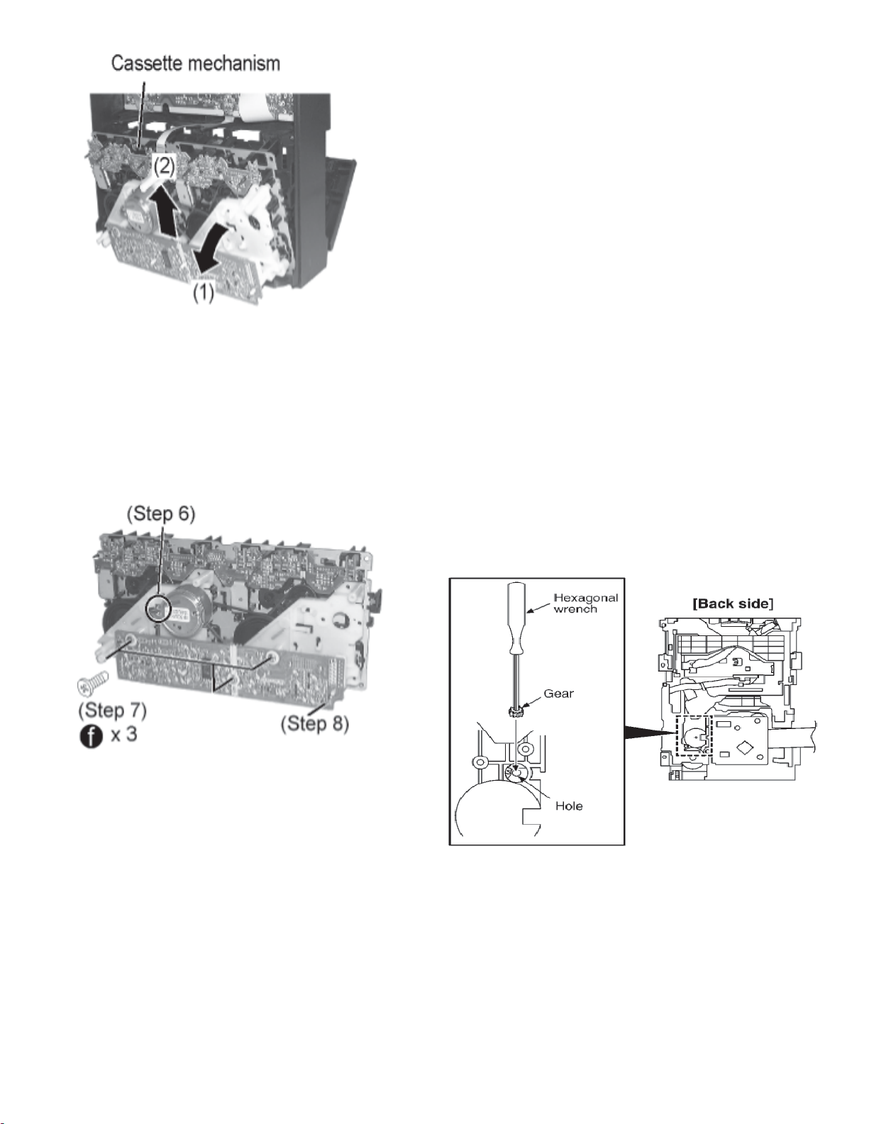
Step 4 Push the lever upward, and then open the cassette lid ass’y
(For DECK1 and DECK2).
Step 5 Tilt the cassette mechanism unit in the direction of arrow
(1), and then remove it in the direction of arrow (2).
10.7 CD Mechanism Main
Component Replacement
Procedures
• Follow the (Step 1) - (Step 4) of Item 10.2 - Disassembly
of Top Cabinet and Rear Panel
• Follow the (Step 1) - (Step 5) of Item 10.2.1 Disassembly for CD Lid
• Follow the (Step 1) - (Step 5) of Item 10.3 - Disassembly
of the CD Mechanism Unit
10.7.1 Replacement of the Traverse
Deck
For replacement of Deck P.C.B.
Step 1 Remove the CD changer unit.
Step 6 Unsolder the motor terminals.
Step 7 Remove 3 screws.
Step 8 Remove Deck P.C.B.
Page 15

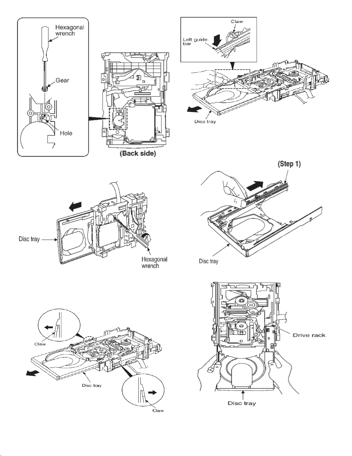
Step 2 Insert the gear with hexagonal wrench into the hole.
Step 7 Remove the traverse deck ass’y from the timing lever.
Caution:
Step 3 Rotate the hexagonal wrench in the direction of arrow
(clockwise), and then open the disc tray fully.
Step 4 With pressing the claw (A), rotate the hexagonal wrench
clockwise. (The slide plate R moves for a little amount.)
Step 5 Pressing the claw (B) in the direction of arrow (1), the
connection lever moves in the direction of arrow (2).
When removing or inserting the traverse deck avoid touching the
OPU lens and pressing onto the turntable
Step 8 Remove 3 screws.
Step 9 Unsolder the motor terminals (4 points).
Step 6 Lift up the traverse deck ass’y.
Step 10 Remove the FFC board from the connector, and then
remove the CD Servo P.C.B.
Page 16
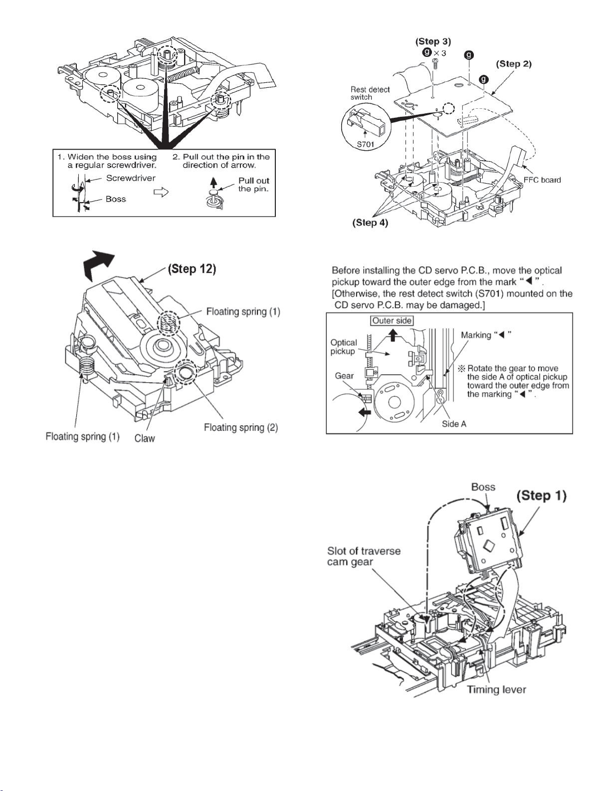
Step 11 Remove the pin.
Note for installation of the CD servo P.C.B.
Step 12 Release the claw, and then remove the traverse deck ass’y.
Note:
Be careful not to lose the 3 floating spring because those will also
be removed on removal of the traverse deck ass’y.
• Installation of the CD Servo P.C.B. after replacement
Step 1 Connect the FFC board.
Step 2 Install the CD servo P.C.B. in the traverse deck ass’y.
Step 3 Remove 3 screws.
Step 4 Solder.
Installation for traverse deck ass’y
Step 1 Install the traverse deck ass’y to the timing lever.
Step 2 Align the boss of traverse deck ass’y with the slot of
traverse cam gear.
Page 17
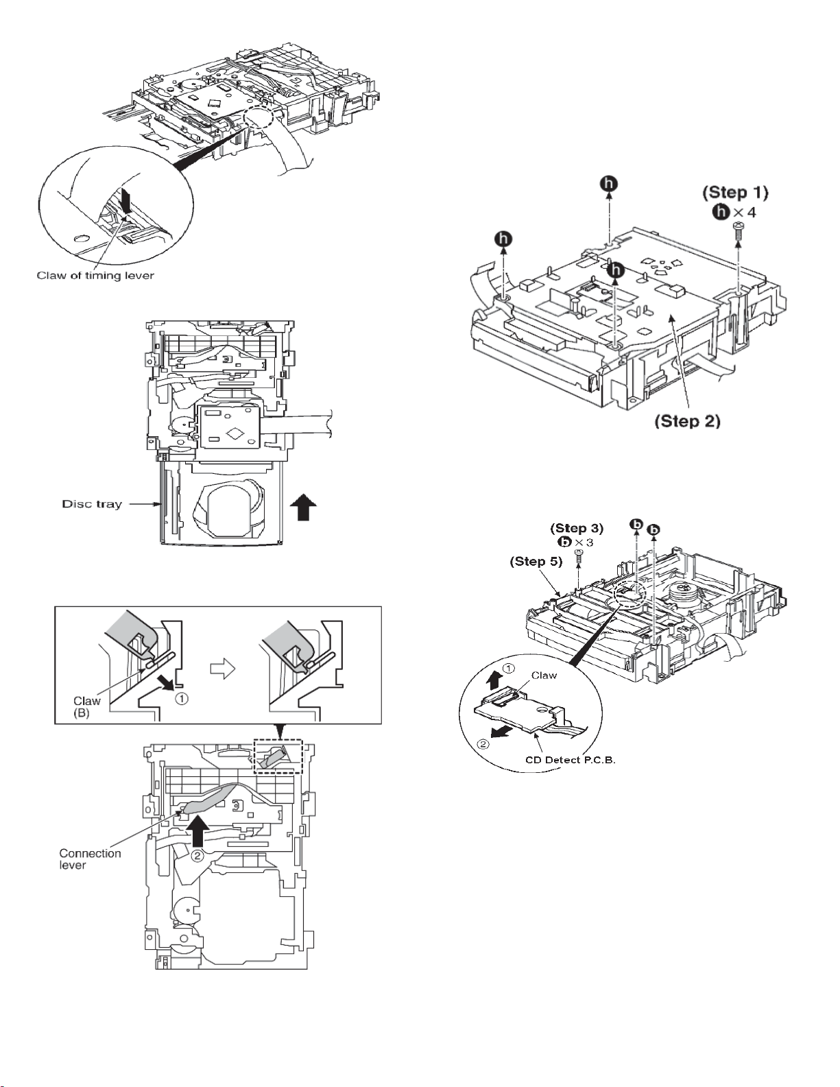
Step 3 Force the claw of timing lever.
10.7.2 Replacement for the Disc
Tray
Step 1 Remove 4 screws
Step 2 Remove the upper plate.
Step 4 Force the disc tray fully.
Step 3 Remove 3 screws.
Step 4 With lifting the claw in the direction of (1), draw the CD
Detect P.C.B. in the direction of arrow (2).
Step 5 Remove the mechanism cover.
Step 5 With pressing the claw (B) in the direction of arrow (1),
force the connection lever in the direction of arrow (2).
Page 18
Step 6 Insert the gear with hexagonal wrench into the hole
Step 7 Rotate the hexagonal wrench in the direction of arrow, and
then open the disc tray fully.
Step 9 With forcing the left guide bar manually because the left
guide bar interfers with claw, draw the disc tray.
[Installation of the disc tray after replacement]
Step 1 Slide the drive rack fully in the direction of arrow.
Step 8 Release the both claws, and then draw the disc tray.
Step 2 Holding the drive rack not to move, install the disc tray.
Step 3 Align the drive rack with the drive gear.
Page 19
NOTE:
Force the right guide bar of tray base manually not to move
upwards.
10.7.3 Disassembly and reassembly
for mechanism base drive unit
Step 1 Remove 3 screws.
Step 4 Holding the disc tray manually, push the disc tray in the
direction of the arrow.
Step 2 Release the claw, and then remove the gear holder.
Step 3 Remove the belt and change gear spring.
NOTE:
Take care not to lose the change gear spring.
Step 4 Remove the pulley gear, change gear and UP/DOWN gear.
Page 20
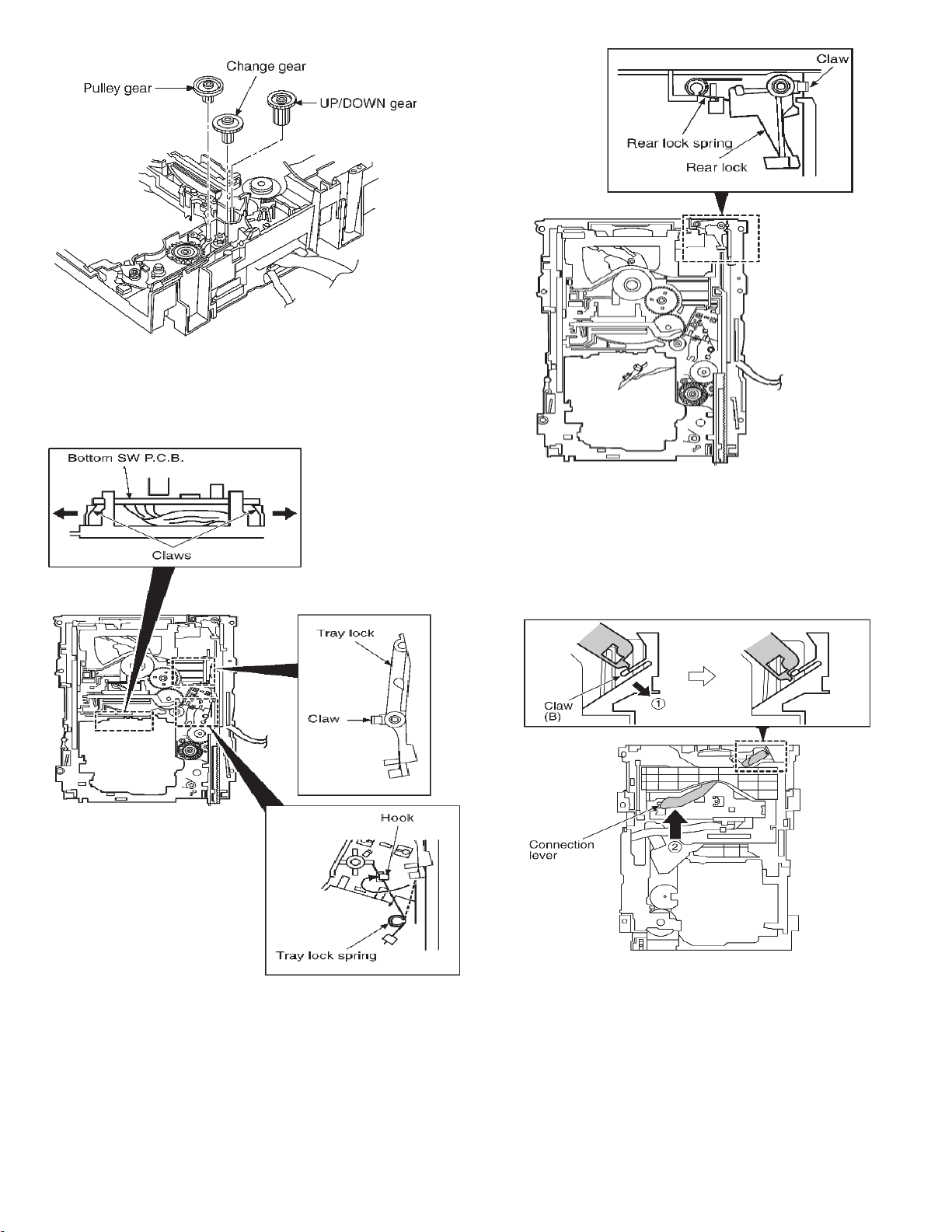
Step 5 Release the 2 claws, and then remove the bottom SW
P.C.B..
Step 9 Pressing the claw (B) in the direction of arrow (1), force
the connection lever in the direction of arrow (2).
Step 6 Install the tray lock spring to hook temporary.
Step 7 Release the claw, and then remove the tray lock.
Step 8 Release the claw, and then remove the rear lock.
Step 10 Move the slide plate 1 to the end of stock side.
Page 21

Step 11 Lift up the left end of spindle base unit in the direction of
arrow (1), and then remove the unit in the direction of arrow (2).
Step 13 Remove the traverse relay gear, traverse cam gear and
drive gear.
Step 12 Remove slide plate 1 and slide plate 2.
[Dissassembly/reassembly for the spindle base unit]
Step 1 Draw the 5 disc spacers.
Page 22

Step 2 Pushing the claw, slide the support plate in the direction of
arrow, and then remove it.
Step 4 Release the 2 claws, and then draw the relay gear B.
Step 5 Release the 2 claws as shown below.
NOTE:
Step 3 Rotate the disc lever in the direction of arrow (1), draw the
disc lever.
NOTE:
Take care not to lose the disc lever spring.
Hold the loading stopper ass’y manually bacause it is flipped by
spring.
Step 6 Remove the cushion spring.
Step 7 Remove the loading stopper ass’y in the direction of arrow.
Page 23

Step 8 Release the 2 claws, and then remove the relay gear A.
Step 9 Release the 2 claws, and then remove the spindle shaft.
Step 12 Squeeze the shaft of lower hook, and then draw it.
Step 10 Remove the lower spindle spring with tweezers.
Step 11 Force the lower hook with thin tip of minus screwdriver.
Step 13 Rotate the lower spindle in the direction of arrow until
the lower spindle interferes with stopper.
Step 14 Insert the thin tip of minus screwdriver between the lower
spindle and UP/DOWN base, and then slacken the lower spindle
to release the stopper. Then, rotate the lower spindle and remove
it.
Page 24

Step 15 Rotate the UP/DOWN base at a 90° angle. Then, spread
the hold bars of loading stopper and remove the UP/DOWN base.
[Installation for loading stopper ass’y]
Step 1 Align the claw of loading stoppers ass’y with the slot of
spindle base. (Caution should be exercised when alignment of
claw due to the size of claws.)
[Reassembly for mechanism base drive unit]
Step 1 Install the traverse cam gear.
Step 2 Rotate the traverse cam gear to the direction of arrow.
Step 2 Lower the loading stopper ass’y, and then align the lower
spindle with the trapezoid tooth of relay gear A.
Step 3 Force the loading stopper ass’y, latch the claw firmly.
Step 3 Install the drive gear and traverse relay gear.
Page 25

Step 7 Move the slide plate 1 to forward fully.
Step 4 Install the slide plate 2 to the mechanism base, and then
match to the connection lever.
Step 5 Install the slide plate 1 to the mechanism base, and then
match to the connection leve and align the trapezoid tooth of
traverse relay gear with the slide plate 1.
Step 8 Install the rear lock. (The claw should be latched.)
Step 9 Install the Spindle Position P.C.B.. (The claw should be
latched.)
Step 10 Install the tray lock. (The claw should be latched.)
Step 6 Install the spindle base unit. (First, slide plate 1.)
Step 11 Remove the tray lock spring from hook,and then latch to
the tray lock.
Step 12 Install the UP/DOWN gear, change gear, change gear
spring, pulley gear and belt in the order of (1) - (5).
Page 26
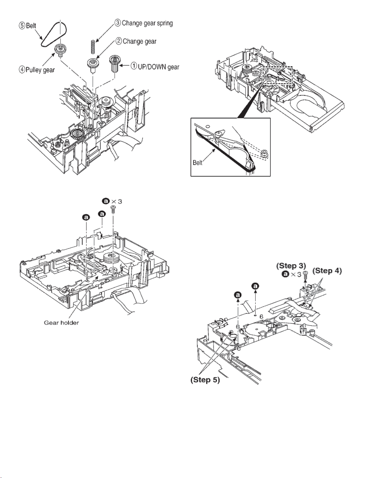
10.7.4 Replacement for the motor
ass’y
Step 13 Install the gear holder, and then tighten the screw (a).
Step 14 Install the tray base, traverse ass’y, mechanism cover and
upper plate.
Step 1 Install the belt temporarily.
NOTE:
Take care not apply the grease to the belt.
Step 2 Upset the CD loading unit.
Step 3 Remove 3 screws.
[Operation check after servicing]
Check the proper operation of following items with gear and
hexagonal screwdriver.
Open/close of tray base.
Moving the tray base to the stock side.
UP/DOWN operation of spindle base unit.
UP/DOWN operation of traverse ass’y.
Step 4 Unsolder the plunger terminals (2 points).
Step 5 Unsolder the motor terminals (2 points).
Page 27
Step 6 Release the 2 claws (A), and then remove the Motor P.C.B.
10.8 Replacement for the pinch
roller ass’y and head block
• Follow the (Step 1) - (Step 2) of Item 10.2 - Disassembly
of Top Cabinet and Rear Panel
• Follow the (Step 1) - (Step 5) of Item 10.2.1 Disassembly for CD Lid
• Follow the (Step 1) - (Step 2) of Item 10.3 - Disassembly
of the CD Mechanism Unit
• Follow the (Step 1) of Item 10.4 - Disassembly the Main
P.C.B. & Transformer P.C.B.
• Follow the (Step 1) - (Step 2) of Item 10.5 - Disassembly
of the Panel P.C.B. & Tact Switch P.C.B.
• Follow the (Step 1) - (Step 5) of Item 10.6 - Disassembly
for the Deck Mechanism Unit & Deck P.C.B.
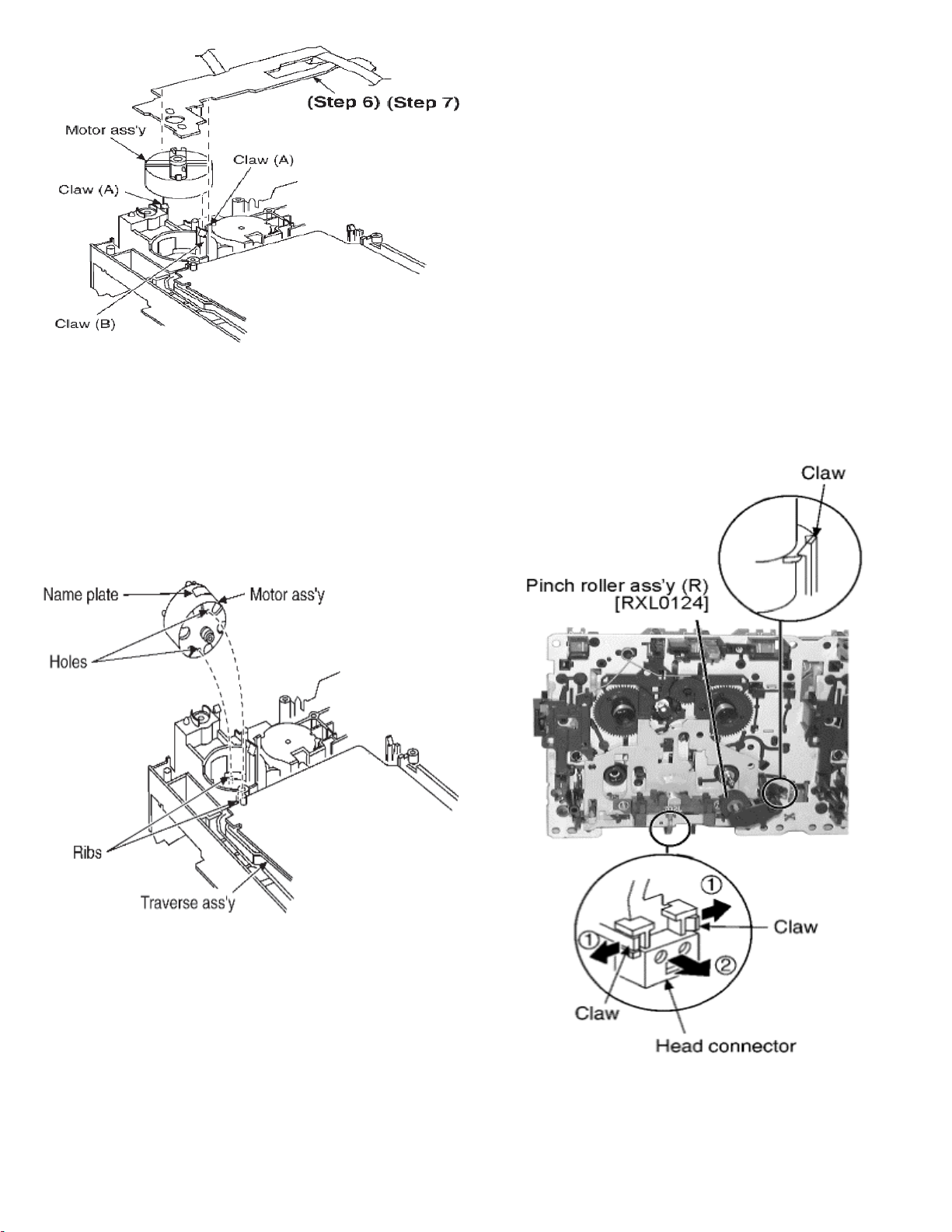
Step 7 Release the claw (B), and then remove the motor ass’y.
[Notice for motor ass’y installation]
Locate the name plate of motor to the traverse ass’y.
Align the hole of motor with the ribs.
* The mechanism as shown below is for DECK1. For the one of
DECK 2, perform the same procedures.
Step 1 Release the 2 claws, and then remove the pinch roller (R),
(F).
Step 2 Release ther 2 claws, and then remove the head connector.
Page 28
Step 3 Remove 2 screws.
10.9 Replacement for the
Deck motor ass’y, capstan
belt A, capstan belt B and
winding belt
• Follow the (Step 1) - (Step 2) of Item 10.2 - Disassembly
of Top Cabinet and Rear Panel
• Follow the (Step 1) - (Step 5) of Item 10.2.1 Disassembly for CD Lid
• Follow the (Step 1) - (Step 2) of Item 10.3 - Disassembly
of the CD Mechanism Unit
• Follow the (Step 1) of Item 10.4 - Disassembly the Main
P.C.B. & Transformer P.C.B.
• Follow the (Step 1) - (Step 2) of Item 10.5 - Disassembly
of the Panel P.C.B. & Tact Switch P.C.B.
• Follow the (Step 1) - (Step 5) of Item 10.6 - Disassembly
for the Deck Mechanism P.C.B.
Step 1 Release the 2 claws, and then remove the head connector.
Step 4 Remove 3 screws.
Step 2 De-solder plunger point.
Step 3 Remove the Deck Mechanism P.C.B.
Page 29
Step 5 Remove the flywheel R.
Step 6 Release the claw of tape side, and then remove the winding
lever and spring.
Step 7 Remove the flywheel F.
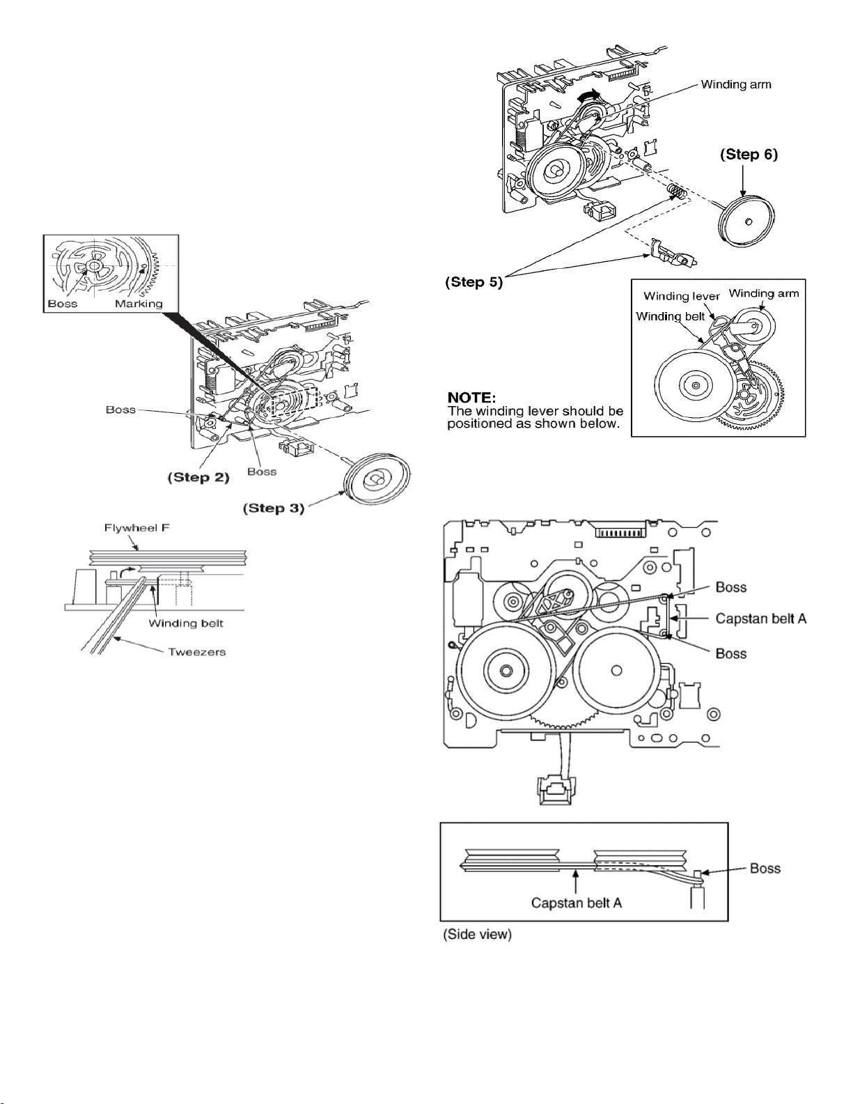
[Installation of the belt]
Step 1 The boss and marking should be positioned horizontally.
Step 2 Put the winding belt on the pulley temporarily.
Step 3 Install the flywheel F.
Step 4 Put the winding belt on the flywheel F.
Step 5 Install the winding lever and spring while pressing the
winding arm in the direction of arrow.
Step 7 Put the capstan belt A temporarily as shown below.
Step 6 Install the flywheel R.
Step 8 Put the capstan belt B on the motor ass’y pulley.
Step 9 Install the sub chassis to the mechanism, and then tighten
screws.
Page 30

Step 10 Remove 3 screws.
Step 11 Put the capstan belt B as shown below.
Step 12 Put the capstan belt A on the motor ass’y pulley.
Page 31

10.10 Replacement for the cassette
lid ass’y
• Follow the (Step 1) - (Step 2) of Item 10.2 - Disassembly
of Top Cabinet and Rear Panel
Step 1 Push the lever upward, open the cassette lid ass’y. (For
DECK1 and DECK2)
10.11 Counter - measure for tape
trouble
• Follow the (Step 1) - (Step 2) of Item 10.2 - Disassembly
of Top Cabinet and Rear Panel
Step 1 If a cassette tape cannot be removed from the deck since
the tape is caught by the capstan or pinch roller during playback
or recording, rotate the flywheel F in the direction of the arrow to
remove the tape.
Step 2 Lift up the cassette lid ass’y in the direction of arrow. (For
DECK1 and DECK2).
Step 3 Remove the cassette lid ass’y. (For DECK1 and DECK2).
Step 2 Push the lever upward and open the cassette lid ass’y. Take
the cassette tape off.
Page 32

11.3 Checking the Panel, Tact
11 Service Position
11.1 Checking Procedur e
Note:
For the disassembling procedure, see Section 10.
11.2 Checking the Main P.C.B.,
Power P.C.B. and Transformer
P.C.B.
Disassembly of Top Cabinet and Rear Panel.
Disassembly of CD Lid.
Disassembly CD Mechanism Unit.
Connect FFC board (CN309 & CN310) from CD Mechanism
Unit.
Switch, Deck& Deck Mechanism
P.C.B.
Remove Top Cabinet and Rear Panel.
Remove CD Lid.
Remove CD Mechanism Unit.
Remove volume knob at front panel.
Remove Panel P.C.B. & Tact Switch P.C.B.
Remove Deck Mechanism Unit.
Use the extension cable (REEX0310 - 10 Pins) to reconnect
(CP600) Panel P.C.B. and (CN971) Deck Mechanism
P.C.B.
Page 33

12.1 Abnormality detection for Deck Mechanism bloc
k
No. Abnormal Items Error Display Method of Detection
1 MODE SW
abnormal
2 REC INH SW
abnormal
3 HALF SW
abnormal
4 Reel pulse
abnormal
H01 Normal operation during mecha transition, MODE SW abnormal is memorized. The content of abnormality can be confirmed in the
abnormal detection mode explained in the later section.
H02 The contect of abnormality can be confirmed in the abnormal detection mode explained in the later section.
H03 The contect of abnormality can be confirmed in the abnormal detection mode explained in the later section.
F01 The contect of abnormality can be confirmed in the abnormal detection mode explained in the later section.
12.2 Abnormality detection for CD/Changer block
No. Abnormal Items Error Display Method of Detection
1 REST SW
abnormal
2 Transmission
error between CD
servo LSI and
micon
3 CLAMP SW
abnormal
4 BOTTOM SW
abnormal
5 POSITION SW
abnormal
6 SW1 abnormal F28 Refer to CR20 control specification section 5-2 [ERROR CODE] table M-02 ~ M-08 error is detected.
F15 Under normal operation (Self-Diagnostic Mode inclusive), this error occurs when the REST SW ON is not detected within the
specified time and shall be memorized.
F26 Under normal operation (Self-Diagnostic Mode inclusive), this error occurs when the selection is set to CD and SENSE=’H’ is
detected and SENSE=’L’ is notdetected within a fail safe time (20ms) after system command transmission was sent.
F16 Refer to CR20 control specification section 5-2 [ERROR CODE] table M-0A error is detected.
F17 Refer to CR20 control specification section 5-2 [ERROR CODE] table M-09 error is detected.
F27 Refer tp CR20 control specification section 5-2 [ERROR CODE] table M-05 ~ M-08 error is detected.
7 SW2 abnormal F29 Refer to CR20 control specification section 5-2 [ERROR CODE] table M-02 ~ M-08 error is detected.
8 OPEN SW
abnormal
H15 Refer to CR20 control specification section 5-2 [ERROR CODE] table M-01 error is detected.
12.3 Power supply related error detection
No. Abnormal Items Error Display Method of Detection
1 POWER AMP
output abnormal
F61
During normal operation, if DCDET becomes ‘L’, normal POWER OFF process shall not be executed, PCNT shall be switched to ‘L’
immediately. GOODBYE shall not be displayed andthe error display F61 will be displayed instead.
2 seconds after the F61 display, ECONO shall be set to ‘L’ and FL display shall be turned off.
The error content shall be memorized when the abnormality occurs and can bedisplayed in the C-mecha self-diagnostic mode
described later.
Page 34

13 Self-Diagnostic Function
13.1 Self-diagnostic display
13.3 Cassette Mechanism Test (For
error code H01, H02, H03, F01,
F02)
This unit is equipped with a self-diagnostic display function
which, if a problem occurs, will display an error code
corresponding to the problem.
Use this function when performing maintenance on the unit.
13.2 How to enter the SelfDiagnostic Function
TOP PREVIOUS NEXT
Press “TAPE, DECK 1/2” to select Deck 2.
Load a cassette tape with the erasure prevention tab, remove
from left side only and close the cassette holder.
Press “FAST FORWARD MEMORY” (Tape will be stop after
2 seconds)
Load a cassette tape with the erasure prevention tab, remove
from right side only and close the cassette holder.
Press “REVERSE FM MODE/BP” (Tape will be stop after 2
seconds)
Load a pre-recorded tape with both side record tabs intact and
close the cassette holder.
Press “PLAY/TUNE/TIME ADJ UP” (After TPS function,
tape will stop automatically)
Press “REC/STOP” (Tape will not move)
Press “STOP/TUNE MODE” to indicate Error code.
• If several problem exist, error code will change each time
when “ /STOP” is pressed.
(e.g. H01 ! H03 ! F01 .....etc.)
Press “TAPE, DECK 1/2” to select Deck 1.
Repeat step 2 to 9 to test Deck 1. (Tape Deck 1 will not check
H02 because of no recording function)
Page 35

13.4 CD Mechanism Test (F15, F26,
F16, F17, F27, F28, F29, H15)
Press “CD”.
Press “OPEN/CLOSE (1)” and place a CD.
Press “OPEN/CLOSE (1)” to close the tray.
Press “OPEN/CLOSE (5)” and wait until the tray is open.
Press “OPEN/CLOSE (1)” and remove the CD.
Press “OPEN/CLOSE (1)” to close the tray.
Press “/STOP” to indicate Error Code.
• If several problem exist, error code will change each time
when “/STOP” is pressed. (e.g. F15 ! F26 ! F16 ....etc).
13.5 To clear all Error code
14 CD Test Mode Function
This CD test mode is provided to check CD unit without
connecting to changer loading mechanism. This mode shall
operate CD PLAY with CD unit being connected only and CD
Automatic Alignment result is shown on FL display.
14.1 How to set CD test mode
Press “STOP/TUNE MODE” button for 5 seconds.
FL indicator shows “CLEAR” for 1 second and change to
“T”.
13.6 How to get out from SelfDiagnostic function
Press “Power” button OFF.
13.7 Power Amplifier Failure (F61)
When power amplifier fail, F61 will indicate automatically.
Page 36

14.2 CD Automatically Adjustment
15 Measurements and
result indication
Under CD test mode, pressing the numeric key ‘0’ on the remote
controller will display the auto adjustment result. FLOCK,
TLOCK and CLVS status shall be shown as below:
During the above display, executing CD PLAY will display auto
adjustment result for CD PLAY mode.
Adjustments
15.1 Cassette Deck Section
• Measurement Condition
• Make sure head, capstan and press roller are clean.
• Judgeable room temperature 20 ± 5 °C (68 ± 9°F)
• Measuring instrument
• EVM (DC Electronic voltmeter)
• Digital frequency counter
• T est Tape
• Tape speed gain adjustment (3 kHz, -10 dB); QZZCWAT
15.1.1 Tape Speed Adjustment
(Deck 1/2)
Set the tape edit button to “NORMAL” position.
Insert the test tape (QZZCWAT) to DECK 2 and playback
(FWD side) the middle portion of it.
Adjust Motor VR (DECK 2) for the output value shown
below.
Adjustment target: 2940 ~ 3060 Hz (NORMAL speed)
After alignment, assure that the output frequency of the
DECK 1 FWD are within ±60 Hz of the value of the
output frequency of DECK 2 FWD.
Fig.1
Page 37

15.1.2 Bias and Erase Voltage
15.1.3 Bias Frequency Adjustment
Check
Set the unit “AUX” position.
Insert the Normal blank tape (QZZCRA) into DECK 2 and
the unit to “REC” mode (use “• REC/STOP” key).
Measure and make sure that the output is within the standard
value.
Bias voltage for Deck 2 14±4mV (Normal)
Erase voltage for Deck 2 80mV (Normal)
Fig.2
(Deck 1/2)
Set the unit to “AUX” position.
Insert the Normal blank tape (QZZCRA) into DECK 2 and
set the unit to “REC” mode (• use “REC/STOP” key).
Adjust L1002 so that the output frequency is within the
standard value.
Standard Value: 97 ±8 kHz
Fig.4
Fig.3
15.2 Tuner Section
15.2.1 AM-IF Alignment
Connect the instrument as shown in Fig.5.
Set the unit to AM mode.
Apply signal as shown in Fig. 5 from AM-SG.
Adjust Z102 so that the output frequency is maximized in
Fig. 6.
Fig.5
Page 38

Connect the instrument as shown in Fig. 7.
15.3 Alignment Points15.2.2 AM RF Adjustment
Set the unit to AM mode.
Set AM-SG to 520kHz.
Receive 520kHz in the unit.
Adjust Z101 (OSC) so that the EVM-AC is maximized.
Set AM-SG to 600Hz.
Receive 600Hz in the unit.
Adjust Z101 (ANT) so that the EVM-SG is maximized.
Set AM-SG to 520kHz.
Receive 520kHz in the unit.
Adjust Z101 (OSC) so that the EVM-DC value is with
1.1±0.5V.
Fig.7
15.3.1 Cassette Deck Section
15.3.2 Adjustment Point
Page 39

FM ANT
AM ANT
Z120
Q1
Q3
Q2
MIXER
OSC
Q4
BUFFER
1
RF AMP
5
CF201
7
Q101
IF AMP
CF202
FM
AM
ANT
COIL
Z101
AM
OSC
COIL
B
346
B
(FM)
8
RCH
PHASE
DET
VCO
FF FF
DECODER
STEREO
SWITCH
1316 15 14
PILOT
CANCEL
PILOT
FF
DET
24 23 22
ALC
AM
OSC
BUFFER
LEVEL
DET
FM
IF
12 3
S-CURVE
FM
DET
REG
21 20 19 18
AM
AM
RM AMP
MIX
AGC
AM
IF
AM/FM
IF
BUFFER
456
COMP
TUNING
DRIVE
SD
DET
7
17
AM
ST
REG
9810 11 12
B
IC101
LA1833NMNTLM
FM/AM IF AMP,
DET/AM OSC,
MIX/FM MPX
Z102
AM
IFT
X102
DO/ST
SD
16
17
18
11
15
B
B
PHASE DETECTOR
CHARGE PUMP
DETECTOR
POWER ON
RESET
Q106
TUNER
15V
SUPPLY
SWITCH
B
(FM)
UNLOCK
UNIVERSAL
COUNTER
19
REFERENCE
DIVIDER
SWALLOW COUNTER
1/6,1/17,4 BITS
12 BITS PROGRAMMABLE
DIVIDER
SHIFT REGISTER LATCH
10
7
1
2
6
8
9
IC102
LC72131MDTRM
PLL FREQUENCY SYNTHESIZER
C2B
I/F
X103
1
20
14
12
13
B
5
DO
CE
2
3
DI
4
CL
ST/DO
PLLDA
PLLCLK
CE
A
TO CD DRIVE BLOCK
Page 40

GRID11
GRID1
4,5,7,8,10,11,13,14,16,17,19,20,
22,23,25,26,28,31,33,35,37,40
FL DISPLAY
FL600
SEG1
SEG16
3,6,9,12,15,18,21,24,27,
29,30,32,34,36,38,39
FROM POWER
TRANSFORMER
PLLDA
STAT
ST/DO
PLLCLK
BLKCK
CD_RST
SD
MLD
MDATA
MCLK
CE
21~24,27~33
GRID1
GRID11
XTB
XT
47
46
IC603
C0JBAE000192
XOR GATE
43
4
1
SCK
CSB
SI
RSTB
41
42
44
IC602
C0HBB0000040
FL DRIVER
IC1
C0GAM0000005
MOTOR DRIVE
5
IN1
6
IN2
REG
3~12,15~20
SEG1
SEG16
OUT1
OUT2
8
VS
B
2
10
M
D1
RM1
Q1
POWER
SUPPLY
CONTROL
B
SW5
LOAD
D2
PUSH
PUSH
OPEN
SW4
CD
B
SW2
SW1
SW3
86
90
CHG_AD1
87
CHG_SW1
CHG_SW2
89
CHG_AD2
Q302
SWITCH
79
80
81
25
MLD
MDATA
MCLK
PLLCE
Q303
SWITCH
22
VCC
VREF
4
GND
7
1
B
Q324
CD
MOTOR
B
SUPPLY
SWITCH
Q323
PLUNGER
MOTOR
SUPPLY
CONTROL
SWITCH
71
FL_RESET
73
72
FL_CS
FL_DOUT
85
84
CHG_CW
CHG_CCW
C2CBJF000017
IC305
88
CHG_PLR
MICROPROCESSOR
83
CHG_HLF
74
23
19
77
SD
BLKCK
CD_RST
PLLCK
24
21
78
ST/DO
STATUS
PLLDA
FL_CLK
S701
REST SW
82
/RESTSW
V_JOG_A
67
VR600
JOG VOL
68
V_JOG_B
MBP2
7
Q313, Q314
SWITCH
X_IN
MBP1
15
6
X_OUT
13
X303
Page 41

(DECK 1)
P.B. HEAD LCH
(DECK 2)
R/P HEAD LCH
4
2
IC1004
C1AA00000612
R/P SELECT
Q1017
MOTOR
SWITCH
M
M1002
(DECK 2)
ERASE HEAD
3
5
(BEAT PROOF/
Q325
REC:
ON/OFF
CONTROL
B
SWITCHING
RECH)
Q1001,Q1003
IC1001
AN7348S-E1
P.B EQ/REC AMP/
ALC/TPS AMP
24(23)
1(2)
22(3)
21(4)
17(8)
6
19
15
12
L1002
Q322
SUPPLY
CONTROL
SWITCH
+
-
LOGIC L/H
ALC
NOR/CrO &
HI/LO LOGIC
LOGIC
REC/PB
9
B
RIPPLE
REJECTION
11
BIAS OSC
CONTROL
Q1004,Q1005,
Q1007
SWITCH
Q319
Q1014(Q1015)
20(5)
18(7)
10
16
14
13
Q320,Q321
REC:ON/OFF
CONTROL/
SWITCH
BP
Q1012
(Q1013)
MUTING
B
Q1016
DECK
MUTING
SWITCH
Q318
DECK
MUTING
CONTROL
SWITCH
BUFFER
AMP
Q1020
(Q1021)
MUTING
SWITCH
(MODE)
S951
53
52
MODE_1
IC951
CNB13030R2AU
PHOTO
INTERRUPTER
(HALF)
S952
HALF_1
Q326
SWITCH
B
Q612
SWITCH
PHOTO:ON/OFF
Q616
SWITCH
PHOTO:ON/OFF
55
PHOTO_1
Q615, Q619
PLUNGER
SUPPLY SWITCH/
PLUNGER:ON/OFF
SWITCH
56
PLG1
Q617, Q618
PLUNGER
SUPPLY SWITCH/
PLUNGER:ON/OFF
XC_IN
10
X301
D951
SWITCH
D971
57
PLG2
XC_OUT
11
Q610
SWITCH
PHOTO:ON/OFF
Q611
SWITCH
PHOTO:ON/OFF
54
PHOTO_2
C2CBJF000017
/CD
75
Q310
CD ON/OFF
SUPPLY
SWITCH
B
58
66
MTR
MICROPROCESSOR
IC305
D307
BP1
Q308, Q309
CURRENT
CONTROL/
VOLTAGE
STABILISER
CD 3.3V
60
59
REC
65
DMT
DECK1_H
B
B
IC971
CNB13030R2AU
PHOTO
INTERRUPTER
(MODE)
91
DECK2
Q328
SWITCH
B
(F.REC INH)
S975
S971
B
Q327
SWITCH
Z971
(HALF)
S972
INTERFACE
B
Page 42

AUX
JK300
CD SIGNAL
4(39)
5(38)
9(34)
8(35)
6(37)
3(40)
IN B1(2)
IN C1(2)
A_VOLIN1(2)
REC1(2)
IN D1(2)
IN A1(2)
IC300
C1BB00000747
AUDIO SOUND
PROCESSOR
CLOCK
DATA
22
21
OUT1(2)
19(24)
MUTE_H
Q407
(Q207)
MUTING
SWITCH
Q301
MUTING
CONTROL
SWITCH
IC301
C0AABB000117
HEADPHONE AMP
3(5)
Q401(Q201)
AUDIO
AMP
AGC
SWITCH
B
1(7)
Q402
(Q202)
MUTING
SWITCH
Q403(Q203)
HEADPHONE
MUTING
SWITCH
B
HP_L(R)
Q409
SWITCH
1(2)
LM_L(R)
D404
C2CBJF000017
26
27
ASP_DAT
MICROPROCESSOR
IC305
ASP_CLK
39
MUTE_H
40
MUTE_A
B
D312
B
12
/RESET/EFP_RESET
CONTROL
B
D306
B
B
Q315
POWER
RESET
SWITCH
D303
D304,D305
D302
KEY SW
47
DCDET
92~94
KEY1
KEY3
SYNC
PCONT/EFP_/CE
20
46
Q312
PCONT
SWITCH
Q316,
SSEQ_LED
76
Q614
D929
B
LED
DRIVE
RMT
18
Z600
Q317
POWER
SUPPLY
SWITCH
B
REMOTE SENSOR
Page 43

10(14)
11(13)
-IN L(R)
+IN L(R)
IC501
RSN35H2A-P
POWER HIC
OUT L(R)
+VCC
-VCC
4(1)
2
3
LCH
+
JK952
-
FULL RANGE
FAN
DC_DET
FAN
HP _SW
MUTE_H
SYNC
D513
7
12
9
MUTE C
IN GND
GND
HEADPHONE
SYNCHRONISING
Q512,Q513
DC DETECT
Q514
MUTING
SWITCH
Q952
SWITCH
FILTER
FILTER
SWITCH
AC DET
LATCH
-VCCM
Q501
10V VOLTAGE
REGULATOR
6
5
FILTER
8
B
Q502,Q505
VOLTAGE SUPPLY/
CURRENT CONTROL
SWITCH
JK601
HEADPHONE
RCH
Q950
SYSTEM 6V
VOLTAGE
B
REGULATOR
D961~D964
DC_DET
HP_SW
SYNC
SIGNAL LINES
MAIN SIGNAL LINE
FM OSC SIGNAL LINE
FM SIGNAL LINE
( )
Indicates the Pin No. of Right Channel.
Q503
15V VOLTAGE
B
REGULATOR
Q504,Q506,Q507Q508
5V VOLTAGE
B
REGULATOR
CURRENT STABILISER/
LIMIT SWITCH/
10V VOLTAGE REGULATOR
B
CD SIGNAL LINE
AM OSC SIGNAL LINE
AUX SIGNAL LINE
D954~D957
Q951
VOLTAGE
REGULATOR
(-VP)
FP533
FP950
D959
TO
FL DISPLAY
AM SIGNAL LINE
FM & AM SIGNALS LINE
CD-DA SIGNAL LINE
D950~D953
FP951
T950
POWER TRANSFORMER
Q953
POWER
SWITCH
CONTROL
PLAYBACK SIGNAL LINE
RECORDING SIGNAL LINE
RL950
T951
B
SUB
TRANSFORMER
JK950
F1
AC INLET
E500
NOTE : Signal lines are applicable to the Left Channel only.
Page 44

FM ANT
AM ANT
Z120
Q1
Q3
Q2
MIXER
OSC
Q4
BUFFER
1
RF AMP
5
CF201
7
Q101
IF AMP
CF202
FM
AM
ANT
COIL
Z101
AM
OSC
COIL
B
346
B
(FM)
8
RCH
PHASE
DET
VCO
FF FF
DECODER
STEREO
SWITCH
1316 15 14
PILOT
CANCEL
PILOT
FF
DET
24 23 22
ALC
AM
OSC
BUFFER
LEVEL
DET
FM
IF
12 3
S-CURVE
FM
DET
REG
21 20 19 18
AM
AM
RM AMP
MIX
AGC
AM
IF
AM/FM
IF
BUFFER
456
COMP
TUNING
DRIVE
SD
DET
7
17
AM
ST
REG
9810 11 12
B
IC101
LA1833NMNTLM
FM/AM IF AMP,
DET/AM OSC,
MIX/FM MPX
Z102
AM
IFT
X102
DO/ST
SD
16
17
18
11
15
B
B
PHASE DETECTOR
CHARGE PUMP
DETECTOR
POWER ON
RESET
Q106
TUNER
15V
SUPPLY
SWITCH
B
(FM)
UNLOCK
UNIVERSAL
COUNTER
19
REFERENCE
DIVIDER
SWALLOW COUNTER
1/6,1/17,4 BITS
12 BITS PROGRAMMABLE
DIVIDER
SHIFT REGISTER LATCH
10
7
1
2
6
9
IC102
LC72131MDTRM
PLL FREQUENCY SYNTHESIZER
C2B
I/F
8
X103
1
20
14
12
13
B
5
DO
CE
2
3
DI
4
CL
ST/DO
PLLDA
PLLCLK
CE
A
TO CD DRIVE BLOCK
Page 45

GRID11
GRID1
4,5,7,8,10,11,13,14,16,17,19,20,
22,23,25,26,28,31,33,35,37,40
FL DISPLAY
FL600
SEG1
SEG16
3,6,9,12,15,18,21,24,27,
29,30,32,34,36,38,39
FROM POWER
TRANSFORMER
PLLDA
STAT
ST/DO
PLLCLK
BLKCK
CD_RST
SD
MLD
MDATA
MCLK
CE
21~24,27~33
GRID1
GRID11
XTB
XT
47
46
IC603
C0JBAE000192
XOR GATE
43
4
1
SCK
CSB
SI
RSTB
41
42
44
IC602
C0HBB0000040
FL DRIVER
IC1
C0GAM0000005
MOTOR DRIVE
5
IN1
6
IN2
REG
3~12,15~20
SEG1
SEG16
OUT1
OUT2
8
VS
B
2
10
M
D1
RM1
Q1
POWER
SUPPLY
CONTROL
B
SW5
LOAD
D2
PUSH
PUSH
OPEN
SW4
CD
B
SW2
SW1
SW3
86
90
CHG_AD1
87
CHG_SW1
CHG_SW2
89
CHG_AD2
Q302
SWITCH
79
80
81
25
MLD
MDATA
MCLK
PLLCE
Q303
SWITCH
22
VCC
VREF
4
GND
7
1
B
Q324
CD
MOTOR
B
SUPPLY
SWITCH
Q323
PLUNGER
MOTOR
SUPPLY
CONTROL
SWITCH
71
FL_RESET
73
72
FL_CS
FL_DOUT
85
84
CHG_CW
CHG_CCW
C2CBJF000017
IC305
88
CHG_PLR
MICROPROCESSOR
83
CHG_HLF
74
23
19
77
SD
BLKCK
CD_RST
PLLCK
24
21
78
ST/DO
STATUS
PLLDA
FL_CLK
S701
REST SW
82
/RESTSW
V_JOG_A
67
VR600
JOG VOL
68
V_JOG_B
MBP2
7
Q313, Q314
SWITCH
X_IN
MBP1
15
6
X_OUT
13
X303
Page 46

(DECK 1)
P.B. HEAD LCH
(DECK 2)
R/P HEAD LCH
4
2
IC1004
C1AA00000612
R/P SELECT
Q1017
MOTOR
SWITCH
M
M1002
(DECK 2)
ERASE HEAD
3
5
(BEAT PROOF/
Q325
REC:
ON/OFF
CONTROL
B
SWITCHING
RECH)
Q1001,Q1003
IC1001
AN7348S-E1
P.B EQ/REC AMP/
ALC/TPS AMP
24(23)
1(2)
22(3)
21(4)
17(8)
6
19
15
12
L1002
Q322
SUPPLY
CONTROL
SWITCH
+
-
LOGIC L/H
ALC
NOR/CrO &
HI/LO LOGIC
LOGIC
REC/PB
9
B
RIPPLE
REJECTION
11
BIAS OSC
CONTROL
Q1004,Q1005,
Q1007
SWITCH
Q319
Q1014(Q1015)
20(5)
18(7)
10
16
14
13
Q320,Q321
REC:ON/OFF
CONTROL/
SWITCH
BP
Q1012
(Q1013)
MUTING
B
Q1016
DECK
MUTING
SWITCH
Q318
DECK
MUTING
CONTROL
SWITCH
BUFFER
AMP
Q1020
(Q1021)
MUTING
SWITCH
(MODE)
S951
53
52
MODE_1
IC951
CNB13030R2AU
PHOTO
INTERRUPTER
(HALF)
S952
HALF_1
Q326
SWITCH
B
Q612
SWITCH
PHOTO:ON/OFF
Q616
SWITCH
PHOTO:ON/OFF
55
PHOTO_1
Q615, Q619
PLUNGER
SUPPLY SWITCH/
PLUNGER:ON/OFF
SWITCH
56
PLG1
Q617, Q618
PLUNGER
SUPPLY SWITCH/
PLUNGER:ON/OFF
XC_IN
10
X301
D951
SWITCH
D971
57
PLG2
XC_OUT
11
Q610
SWITCH
PHOTO:ON/OFF
Q611
SWITCH
PHOTO:ON/OFF
54
PHOTO_2
C2CBJF000017
/CD
75
Q310
CD ON/OFF
SUPPLY
SWITCH
B
58
MTR
MICROPROCESSOR
IC305
D307
66
BP1
Q308, Q309
CURRENT
CONTROL/
VOLTAGE
STABILISER
CD 3.3V
60
59
REC
65
DMT
DECK1_H
B
B
IC971
CNB13030R2AU
PHOTO
INTERRUPTER
(MODE)
91
DECK2
Q328
SWITCH
B
(F.REC INH)
S975
S971
B
Q327
SWITCH
Z971
(HALF)
S972
INTERFACE
B
Page 47

AUX
JK300
CD SIGNAL
4(39)
5(38)
9(34)
8(35)
6(37)
3(40)
IN B1(2)
IN C1(2)
A_VOLIN1(2)
REC1(2)
IN D1(2)
IN A1(2)
IC300
C1BB00000747
AUDIO SOUND
PROCESSOR
CLOCK
DATA
22
21
OUT1(2)
19(24)
MUTE_H
Q407
(Q207)
MUTING
SWITCH
Q301
MUTING
CONTROL
SWITCH
IC301
C0AABB000117
HEADPHONE AMP
3(5)
Q401(Q201)
AUDIO
AMP
AGC
SWITCH
B
1(7)
Q402
(Q202)
MUTING
SWITCH
Q403(Q203)
HEADPHONE
MUTING
SWITCH
B
HP_L(R)
Q409
SWITCH
1(2)
LM_L(R)
D404
C2CBJF000017
26
27
ASP_DAT
MICROPROCESSOR
IC305
ASP_CLK
39
MUTE_H
40
MUTE_A
B
D312
B
12
/RESET/EFP_RESET
CONTROL
B
D306
B
B
Q315
POWER
RESET
SWITCH
D303
D304,D305
D302
KEY SW
47
DCDET
92~94
KEY1
KEY3
SYNC
PCONT/EFP_/CE
20
46
Q312
PCONT
SWITCH
Q316,
SSEQ_LED
76
Q614
D929
B
LED
DRIVE
RMT
18
Z600
Q317
POWER
SUPPLY
SWITCH
B
REMOTE SENSOR
Page 48

10(14)
11(13)
-IN L(R)
+IN L(R)
IC501
RSN35H2A-P
POWER HIC
OUT L(R)
+VCC
-VCC
4(1)
2
3
LCH
+
JK952
-
FULL RANGE
FAN
DC_DET
FAN
HP _SW
MUTE_H
SYNC
D513
7
12
9
MUTE C
IN GND
GND
HEADPHONE
SYNCHRONISING
Q512,Q513
DC DETECT
Q514
MUTING
SWITCH
Q952
SWITCH
FILTER
FILTER
SWITCH
AC DET
LATCH
-VCCM
Q501
10V VOLTAGE
REGULATOR
6
5
FILTER
8
B
Q502,Q505
VOLTAGE SUPPLY/
CURRENT CONTROL
SWITCH
JK601
HEADPHONE
RCH
Q950
SYSTEM 6V
VOLTAGE
B
REGULATOR
D961~D964
DC_DET
HP_SW
SYNC
SIGNAL LINES
MAIN SIGNAL LINE
FM OSC SIGNAL LINE
FM SIGNAL LINE
( )
Indicates the Pin No. of Right Channel.
Q503
15V VOLTAGE
B
REGULATOR
Q504,Q506,Q507Q508
5V VOLTAGE
B
REGULATOR
CURRENT STABILISER/
LIMIT SWITCH/
10V VOLTAGE REGULATOR
B
CD SIGNAL LINE
AM OSC SIGNAL LINE
AUX SIGNAL LINE
D954~D957
Q951
VOLTAGE
REGULATOR
(-VP)
FP533
FP950
D959
TO
FL DISPLAY
AM SIGNAL LINE
FM & AM SIGNALS LINE
CD-DA SIGNAL LINE
D950~D953
FP951
T950
POWER TRANSFORMER
Q953
POWER
SWITCH
CONTROL
PLAYBACK SIGNAL LINE
RECORDING SIGNAL LINE
RL950
T951
B
SUB
TRANSFORMER
JK950
F1
AC INLET
E500
NOTE : Signal lines are applicable to the Left Channel only.
Page 49

17 Schematic Diagram
• S701
: Rest switch
(All schematic diagrams may be modified at any time with
the development of the new technology)
Note:
• SW1
: Push switch
• SW2
: Push switch
• SW3
: Open switch
• SW4
: CD switch
• SW5
: Load switch
• S601
: Open/ Close switch
• S602
: CD 1 switch
• S603
: CD 2 switch
• S604
: CD 3 switch
• S605
: CD 4 switch
• S606
: CD 5 switch
• S612
: Power switch
• S613
: SSEQ switch
• S614
: Preset switch
• S615
• S901
: Rew switch
• S902
: Tuner switch
• S903
: CD switch
• S904
: FF switch
• S905
: Stop switch
• S906
: Deck 2 open switch
• S907
: T ape switch
• S908
: AUX switch
• S909
: Deck 1 open switch
• S910
: Display switch
• S951
: Mode switch
• S952
: Half switch
• S971
: Mode switch
• S972
: Half switch
• S975
: Recinh_F switch
• VR600
: VR Volume Jog
: Record switch
• S616
: Deck 1/2 switch
Page 50

• The voltage value and waveforms are the reference
voltage of this unit measured by DC electronic voltmeter (high
impedance) and oscilloscope on the basis of chassis. Accordingly,
there may arise some error in voltage values and
waveformsdependingupon the internal impedance of the tester or
the measuring unit.
No mark : Playback << >> : Rec < > : FM
(( )) : CD
• Importance safety notice :
Components identified by
mark
have special characteristics important for safety.
Furthermore, special parts which have purposes of fireretardant (resistors), high-quality sound (capacitors),
low-noise (resistors), etc. are used. Whenreplacingany of
components, be sure to use only manufacturer´s specified
parts shown in the parts list.
Caution !
IC, LSI and VLSI are sensitive to static electricity.
Secondary trouble can be prevented by taking care during repair.
• Cover the parts boxes made of plastics with aluminium
foil.
• Put a conductive mat on the work table.
• Ground the soldering iron.
• Do not touch the pins of IC, LSI or VLSI with fingers
directly.
Page 51

SCHEMATIC DIAGRAM - 1
OPTICAL
PICKUP CIRCUIT
: +B SIGNAL LINE
CD SERVO CIRCUIT
: CD-DA SIGNAL LINE
C3 0.22
VR1
R701
Q701
R750
5.6
4.7
C701
6.3V33
C714
6.3V100
1234
LPD
A
1
1
VCC
2
2
F
3
3
E
4
4
12
E
11
VREF
10
A
9
NC
8
LPD
7
GND
GND
VCC
LDG
1
C2 0.22
2
F
C1
3
B
LD
0.47
4
5
6
5
6
7
8
9
10
11
12
13
14
15
16
CN701
10
11
12
13
14
15
16
5
6
7
8
9
LD
LD GND
GND
B
GND
A
VREF
LPD
GND
T-
T+
F-
F+
C751
0.1
C713
C750
0.1
0.1
C770
0.1
LD
VCC
3132
C712
0.1
R738
6.8K
C711
0.1
R737
6.8K
Q701
B1ADCF000001
LASER POWER DRIVE
29
52662572482392210211120121913 14
EQSW
RFOUT
AN22004A-NF
F
DCB
RF VOLT
C702 0.47
C705 0.1
RFIN
CAGC
IC701
SERVO AMP
E
TBAL
27282930
41
30
R742 10K R743 4.7K
C707 0.039
CEA
ARF
FBAL
GCTL
39
R708 0
C747
470P
R744
34
39K
R706
(ENV) 3TOUT
FEOUT
1K
C703 6.3V100
C706 10
DCDET
FEN
C710
470P
R702
4.7K
R704
R707 0
R729 1.5K
C704 0.1K
C716 680P
BDO
OFTCONT
TEN
TEOUT
R705
39K
3900P
32
1K
C749
OFTR
VREF
42
15 16
/RFDET
EQ8ST
18 17
C742
0.047
40
LDON
GND
33
R728 18K
C735
0.1
C734
10V220
R727
1.5K
21
NC
VCC
22
VREF
23
IN4
24 25 26
IN3
RSTIN
NC
D3+
171615
D4-
NC
D4+
PGND2
GND
PVCC2
14
D3-
R749
18K
IC703
R736
D1+
D1-
NC
920101911181213
8
35
M702
SP MOTOR
38
M701
TRV MOTOR
IN1NCPC2NCIN2
7
NC
R735
100
/RST
12
3456
C738
0.047
R725
R723
560
5.6K
D2+
D2-
C737 0.1
36
M
C736 0.1
37
M
GND
PGND1
PVCC1
10
C715
0.22
C752
0.01
R731
22K
R739
C739
1K
0.01
IC703
AN8739SBTE2
FOCUS COIL/
TRACKING COIL/
TRAVERSE MOTOR/
SPINDLE MOTOR DRIVE
R715
2.7K
Page 52

SCHEMATIC DIAGRAM - 2
: +B SIGNAL LINE : CD SIGNAL LINE
CD SERVO CIRCUIT
: CD-DA SIGNAL LINE
R711
82K
C729 0.1
C717
0.1
R709
100K
C757
6.3V100
C758
0.1
C755
40
39
38
37
36
35
34
33
32
31
30
29
28
27
26
25
24
23
22
21
0.1
1000P
IREF
ARF
LDON
BDO
NRFDET
OFT
RFENV
TE
FE
FBAL
TBAL
IOVDD1
FOM
FOP
TRM
TRP
TRVM(PC)
TRVP
SPOUT
DVDD2
R721
100
C744
C741
20
C718
0.015
0.082
R712
820
41
43
444546
42
DSLF
ADPVCC
(DRF)RFSW
A2
A3
DVSS2
18
19
17
A3A2A1A0A9A4A5A6A7A8CASD3D2
48
49
50
47
PLLF
OUTL
AVSS1
AVSS2
PLLFO
AVDD2
IC702
MN6627934CH
SERVO PROCESSOR
DIGITAL SIGNAL PROCESSOR/
DIGITAL FILTER/
D/A CONVERTER
A5A4A9
A0
A1
16
11
14
1213
15
51
OUTR
10
C740
0.1
52
AVDD1
A8A7A6
53
DVSS3
(NCAS1)
A10
8
9
A10
C730
0.1
54
DVDD3
TMOD2
D3
NCAS0
7
6.3V220
25
R761 10K
56
55
EXT2
FLAG
NRAS
D2
6
5
R717
1K
R718
1K
C731
R762 10K
R763 10K
59
57
58
EXT0
EXT1
D1
NEW
4
2
3
RASWED1
C723
6.3V220
C724
0.1
60
TX
IOVDD2
DRVDD
D0
1
D0
1000P
1000P
MCLK
MDATA
MLD
BLKCK
PWMSEL
SMCK
SBCK
STAT
NRST
SPPOL
PMCK
DQSY
TXTD
TXTCK
NTEST
OUT X2
IN X1
DVSS1
DVDD1
MON
C725
C726
24
22
C727
50V1
C728
50V1
23
C753
470P
R760
12
11 10 9
61
62
63
64
65
66
67
R753 10
68
69
70
71
72
73
74
75
76
77
78
79
80
100
8
7
C722
12P
R720
1M
X701
RSXB16M9J02T
R714
C721
220
12P
C780
0.1
16
LCH OUT
19
A.GND
18
RCH OUT
17
+3.3V
16
D.GND
15
LD SW
14
TX
13
+7.5V
P.GND
MCLK
MDATA
MLD
NC
BLKCK
NC
NC
STAT
/RST
REST SW
13
12
11
10
9
8
7
6
5
4
3
2
1
CN702
TO
MAIN
CIRCUIT
(CN310) ON
TIC
SCHEMA
DIAGRAM-5
C743
0.1
C733
0.1
D2
D3
242526
D3
D2
VSS
VCC
1234
/CAS
WE
D1
D0
D1
D0
A9
CAS
21
2223
20
A9
NC
/OE
IC704
C3ABMB000027
16M DRAM
NC
NC
RAS
6197
5
RAS
WE
A8
A7
18
A8
A7
A0
A10
81791610
A10
A0
A1
A6
A6
A1
A5
A5
A2
111412
A2
A4
15
A4
VSS
A3
VCC
13
C781
0.1
A3
C748
0.1
C746
0.1
C782
0.1
REST SW
15
S701
1
Page 53

FM EXT
ANT
75 OHM
GND
AM LOOP ANT
AM EXT
ANT
JK101
SCHEMATIC DIAGRAM - 3
TUNER/MAIN CIRCUIT
TUNER PACK CIRCUIT
5.6P 2SK544
1
1
2
2
3
3
4
4
5
R110
AM ANT COIL
2
1
Z101
RLA2Z007-T
1K
2.7K
100K
C107
0.047
1000P
100K
220
4.7P
2.2P
3
AM OSC COIL
8
7
9
C108
R112
100K
8P
100K
: +B SIGNAL LINE
: FM/AM SIGNAL LINE
2.2P
2SC2786M
1.2U
18P
3.3P
680K
180P
390
560K
2SC1675l1l2
2.2P
2SC2787FL1TA
C136
4
5
6
1000P
R119
3.3K
1000P
680K
390
390
R118
3.3K
0.47U
5.6P
C114
50V3.3
7
6
8
: FM SIGNAL LINE
: FM OSC SIGNAL LINE
CF201
RLFFETWND01M
1
3
2
C101
0.01
R120
47K
C109
1000P
2324
AFC
OSC
OSC OUT
C104
1000P
R105
470
C102
16V10
C119
680P
2122
AM RF IN
R103
AGC
270
C103
0.01
R106
470K
C115
50V4.7
AM OUT
IC101
C116
0.033
DET OUT
R107
330
RLFFETWND01M
R101
0
Q101
R121
22K
R143
22K
150P
C131
: AM SIGNAL LINE
: AM OSC SIGNAL LINE
R104
1K
CF202
1
3
2
Q101
2SC2058SPTA
FM IF AMP
C120
16V10
C138
0.01
C139
50V4.7
0.01
C118
68K
4.7K
R123
R102
C137
3300P
16101511141213
RCH
MPX IN
PILOT IN
PILOT OUT
Q106
Q106
B1GCCFJJ0015
TUNER 15V
SUPPLY SWITCH
R146
100K
R142
6.8K
R141
6.8K
R145
100K
6800P
C143
C144
6800P
C117
0.01
LCH
C142
50V1
C141
50V1
D101
B0BC5R000009
R114
5.6K
C110
0.01
R152
0
LA1833NMNTLM
FM/AM IF AMP
DET/AM OSC MIX/
C130
6.3V100
C133
C112
27P
0.01
X103
RSXC7M20S05T
C134
27P
R138
3.3K
R130
10K
IC101
FM MPX
R113
10K
C132
C111
1000P
50V4.7
R115
560
R116
1K
17181920
AIN
VSS
XOUT
AOUT
LC72131MDTRM
PLL FREQUENCY SYNTHESIZER
CL
DI
CE
XIN
1234
R136 1K
R137 1K
PLLDA
CE
R111
390
C125
16V22
C113
1000P
82
R151
PD
VDD
FMIN
AMIN
IC102
LW
DO
51661571481391210
R135 1K
R134 470
DO/ST
PLLCLK
SDC
AM
R117
47K
MONO
STRQ
C127
16V22
G2BAE0000003
R129
27K
11
IFIN
FM
2
1
Z102
C124
100P
FM IF IN
1234
C126
1
3
5
R128
82
REG
AM MIX OUT
C106
0.01
4
6
SD
GND
AM IF IN
5206197188179
C147
1000P
C148
0.01
R126
C129
6.3V100
SD
1K
ST
DO/ST
R125
FM DET
470
C149
0.1
R124
X102
STRQ
VCC
33
R127
RLFDFT22DD
R132
10K
FM/AM
470
C122
R122
MONO
50V1
2.7K
C121
50V0.47
R133
1K
R144
120
R131
120
C123
50V1
TGND
DO/ST
+7.5V
RCH
LCH
PLLDA
DO/ST
PLLCLK
15V
SD
CE
TO
MAIN
CIRCUIT
(2A) ON
SCHEMATIC
DIAGRAM-8
1A
TO
MAIN
CIRCUIT
(2B) ON
SCHEMATIC
DIAGRAM-8
1B
Page 54

TO
DECK
CIRCUIT
(CN1001) ON
SCHEMATIC
DIAGRAM-14
AUX
TO
CD LOADING
CIRCUIT
(CN1) ON
SCHEMATIC
DIAGRAM-11
SCHEMATIC DIAGRAM - 4
: +B SIGNAL LINE
: -B SIGNAL LINE
MAIN CIRCUIT
CR02
1
MOTOR
2
BP1
3
DECK1_H
4
DMT
5
MOGND
6
MOT+B
7
REC_H
8
+15V
9
RECINR
10
RECINL
11
AFGND
12
PBR
13
PBL
14
CN304
C442
C410
0.22
RCH
LCH
JK300
CN309
CHG_CW
14
CHG_HALF
13
CD8V
12
CHG_CCW
11
CLAMP
10
OPEN
9
CD_SW1
8
PGND
7
CD_SW2
6
DGND
5
5V
4
POSITION
3
BOTTOMSW
2
PLUNGER
1
0.22
L305
J0JBC0000019
B0ACCK000005
Q308
D307
D308
D307-D308
B0ACCK000005
R329
330
R201
10K
C201
680
C401
680
R401
10K
R344 22K
R345 12K
C326
0.47
R348 220
R346 22K
R347 12K
D324
Q324
KTA12710YTA
CD MOTOR SUPPLY SWITCH
C321
0.01
Q309
C320
R328
10V22
2.2K
Q324
R324
R325
10K
R327
1K
12
C202
100P
C402
100P
R326
100
R340
10K
R350
10K
R323
15
Q310
: PLAYBACK SIGNAL LINE
: RECORD SIGNAL LINE
MOT10V
REC
+15V
REC_R
C443
R395
47K
0.1
REC_L
PBR
AUXR
AUXL
VREF+
R343
10K
CHG_CW
CHG_HLF
CD8V
CHG_CCW
CHG_AD1
CHG_AD2
CHG_SW1
CHG_SW2
SW5V
R202
3.3K
R402
3.3K
R396
47K
C306
50V1
Q323
CHG_PLR
R349
1K
MOT10V
Q323
B1GBCFJJ0039
PLUNGER MOTOR
SUPPLY CONTROL SWITCH
CD3.3V
D309
B0EAKM000117
CD8V
PBL
HI_L
HI_R
VREF+
EE_CS
EE_CLK
R803
22K
/CD
R802
22K
/DMT
DECK1_H
R444
1.2K
R244
1.2K
C364
330P
SW5V
/BP1
: AUX SIGNAL LINE
: MAIN SIGNAL LINE
MTR
C434
50V1
C234
50V1
C363
0.022
4321
C366
330P
R806
4.7K
EE_DAT
Q308
KTA12710YTA
CURRENT CONTROL
SWITCH
TO
PANEL CIRCUIT
(CP601) ON
SCHEMATIC DIAGRAM-10
8
7654321
KEY3KEY3
KEY1KEY1
KEY2KEY2
D_GND
R440
R240
SSEQ_LED
SSEQ_LED
0
0
C432
IC304
8765
KTC3199GRTA
VOLTAGE STABILISER
9
10
SW5V
FL_CLKFL_CLK
FL_DOUTFL_DOUT
SW5V
0
C232
0
BR93LC46FE2
E-EPROM
(NOT SUPPLIED)
Q309
CD3.3V
DGND
FL_CS
FL_RST
EXP_DAT
EXP_DAT
FL_RST
FL_CS
R245
220
IC304
Q310
B1GCCFGA0005
CD ON/OFF
SUPPLY SWITCH
17
161514131211
LED9V
EXP_CLK
LED9V
EXP_CLK
R445
CN303
220
Page 55

SCHEMATIC DIAGRAM - 5
R206
R204
33
33
R205
R207
33
33
C203
1000P
LHPF
Q202, Q402
B1ABEB000001
MUTING SWITCH
RHPF
C309
R309
10V10
27K
-9.0V
LDL
CD3.3V
CDR
CD7.5V
MCLK
MDATA
MLD
CBLKCK
CCDSTAT
CD_RST
R450 4.7K
RESTSW
MAIN CIRCUIT
Q203, Q403
B1ABEB000001
HEADPHONE MUTING
SWITCH
R203
HP_R
1
R208
3.3K
Q203 Q403
R209
560
C429
50V1
R435
1.5K
R235
1.5K
C229
50V1
R310
56K
Q301
B1GDCFJJ0023
AUDIO MUTING
CONTROL SWITCH
G0C101JA0030
L303
C398 1000P
R382 10K
R380 10K
R369 10K
R368 10K
1K
R366
: +B SIGNAL LINE
: -B SIGNAL LINE
R403
1
HP_L
R404
R409
560
R405
33
R408
3.3K
Q402
Q202
R228
R818
2.2K
Q301
1K
1K
R365
R364
Q207, Q407
B1ABEB000001
MUTING SWITCH
R406
33
33
R407
33
C403
1000P
R428
2.2K
2.2K
MUTE_A
R812 4.7K
1K
R363
R234
100K
16V10
R434
100K
C227
16V10
IC301
C0AABB000117
HEADPHONE AMP
Q201
B1ABCF000131
AGC CONTROL
R813 4.7K
R814 4.7K
10V100
1K
1K
R361
R362
: CD SIGNAL LINE
R432
2.2K
C427
C440
1000P
C240
0.01
C444
470P
C391
24531
PLG1/PLG1
PLG2
P_GND
PHOTO1
PHOTO2
/PHOTO2
/PHOTO1
/PLG2
D401
MA2J72800L
R431
C428
100K
16V10
R433
4.7K
-IN1
C425
100P
+IN1
R426
3.3K
GNDOUT1
R427
56K
C426
47P
1234
IC301
VCC
OUT2
-IN2 +IN2
5678
R227
56K
C225
C226
100P
47P
R232
2.2K
+9.0V
D201
MA2J72800L
R233
4.7K
Q325
SW5V
Q322
C360
50V10
0.1
C395
: MAIN SIGNAL LINE
6897
P_GND
R231
100K
HALF_1
MODE_1
V_JOG_BV_JOG_B
V_JOG_AV_JOG_A
/HALF_1
/MODE_1
R430
1K
Q401
B1ABCF000131
AGC CONTROL
C424
50V1
C224
50V1
R226
3.3K
R225
R230
1K
C228
16V10
REC
MTR
/MTR
Q321
B1GBCFJJ0039
DECK MUTING CONTROL SWITCH
R461
1K
Q326
KTA12710YTA
TO
PANEL CIRCUIT
(CP602) ON
SCHEMATIC DIAGRAM-10
SYS6V
DVREF
MOT10V
MOT10V
MOT10V
R429
12K
R425
47K
R229
12K
PCONTPCONT
DVREF+
C313
0.01
C312
0.01
DECK_2
DECK_2
Q401
47K
Q201
/REC
/BP1
Q320
Q320,Q322
B1GBCFJJ0039
SUPPLY CONTROL SWITCH
Q325
B1GDCFJJ0023
REC:ON/OFF CONTROL
Q318
Q327
Q326
SWITCH
R462
1K
2019 21
1716151413121110
18
RMT
SYNC
VREF+VREF+
D_GND
R820
470
SYNC
RMT
SYS6V SYS6V
-9.0V
Q407
R424
4.7K
C423
C422
100P
0.033
C223
C222
100P
0.033
R224
4.7K
B1GBCFJJ0039
B1GDCFJJ0023
+9.0V
BP1
/DMT
Q319
R463
100
Q328
B1GDCFJJ0023
Q327
B1GBCFJJ0039
SWITCH
D_GND
R456
1.5K
R455
100K
R448
4.7
Q319
BP SWITCH
Q321
SWITCH
Q318
Q328
SWITCH
2322242526
HP_RHP_R
HP_GND
HP_GND
R256
1.5K
R255
100K
R423
2.7K
R223
2.7K
DMT
/CD
SW5V
27
HP_L
MIC_GND
HP_L
Q207
28
MIC_GND
R248
4.7
C421
16V10
C221
16V10
29
+9V+9V
OUT2
CN302
30
OUT1
/RESTSW
/RST
2
1
STAT
3
MLD
MCLK
+7.5V
MDATA
BLKCLK
NC
NC
4
6
8
5
7
TO
SERVO CIRCUIT
(CN702) ON
SCHEMATIC DIAGRAM-2
PGND
10
9
141312
11
LD_SW
CD_GND
CD3.3V
15
RCH_OUT
LCH_OUT
19181716
CN310
AGND
Page 56

SCHEMATIC DIAGRAM - 6
MAIN CIRCUIT
: +B SIGNAL LINE
Q316
B1ACCF000063
SWITCH
SYS6V
VREF+
PCONT
Q316
D313
B0ACCE000003
MCLK
RESTSW
CHG_HLF
CHG_CW
CHG_CCW
CHG_SW1
CHG_SW2
CHG_PLR
CHG_AD2
CHG_AD1
DECK2
KEY3
R884
R885
KEY2
R886
KEY1
REG_2
REG_1
VREF+
VCC
B1GBCFJJ0039
Q312
R338
R805
1K
4.7K
R367
10K
R816
Q317
560P
560P
560P
C381
C383
C380
C332 100P
C331
C330
C329
C328
470K
560P
C384
100P
100P
100P
100P
R815
470K
B1ACCF000063
DECK SUPPLY SWITCH
100
100
100
R312
100K
Q312
PCONT SWITCH
DVREF+
Q317
81
82
83
84
85
86
87
88
89
90
91
92
93
94
95
96
97
98
99
100
560P
C385
MLD
MDATA
80
79
MDATA
MCLK
/RESTSW
CHG_HLF
CHG_CW
CHG_CCW
CHG_SW1
CHG_SW2
CHG_PLR
CHG_AD2
CHG_AD1
DECK2
KEY3
KEY2
KEY1
REG_2
AVSS
REG_1
VREF
AVCC
DEMO SELECTOR
LM_L
1
2
LM_R
LM_L
CDSTAT
MLD
LM_R
3
CD_RST
7778
STATUS
CD_RST
NC
4
RDS_DAT
/CD
SSEQ_LED
76
SSEQ_LED
RDS_CLK
MBP1
RDS_DAT
6
5
RDS_CLK
MBP1
FL_CLK
7475
/CD
7
R394
MBP2
FL_DOUT
73
FL_CLK
FL_DOUT
MBP2
BYTE
8
10K
FL_CS
FL_RST
V_JOG_B
EXP_DAT
EXP_CLK
68
72
69
71
70
FL_CS
EX1_CLK
EX1_DAT
FL_RESET
C2CBJF000017
MICROPROCESSOR
XC_OUT
XC_IN
/RESET/EFP_RESET
CNVSS/EFP_CNVSS
12
9
10
11
XC_IN
X_OUT
XC_OUT
R807
680
R804
330K
R801
10M
H0A327200073
BP1
V_JOG_A
R393 10K
66
67
V_JOG_A
V_JOG_B
IC305
VSS
X_OUT
1413
15
XIN
X301
DMT
C353
100P
R392 10K
C354
100P
65
64
BP1
VSS
DMT
XIN
VCC
/NMI
18
16
17
R332
100
VCC
H2A100500006
63
NC
RMT
RMT
C361
15P
C362
VCC
62
BLKCK
C387
68P
X303
C388
68P
18P
DECK1_H
R391 4.7K
60
61
NC
VCC
BLKCK
SYNC
2019
10K
R400
SYNC
DO/ST
C369
56P
/REC
/MTR
R389 10K
R390 10K
58
59
57
REC
MTR
DECK1_H
ST/DO
PLLCK
SD
PLLCLK/
SD
/PLG1
/PLG2
56
PLG2
PLLDA
2524232221
PLLDA
PLLCE
R810
4.7K
Q313
C359
1000P
/MODE_1
/PHOTO_1
/PHOTO_2
R386 10K
R385 10K
R384 10K
54
55
53
PLG1
PHOTO_1
PHOTO_2
EE_CS/EFP_/EPM
ASP_DAT
ASP_CLK
PLLCE
ASP_DAT
ASP_CLK
C325
100P
/HALF_1
C352 100P
C351 100P
C350 100P
R383 10K
51
52
NC
HALF_1
MODE_1
SP_C
SP_B
SP_A
DCDET
PCONT/EFP_/CE
EE_DAT
EE_CLK
MUTE_A
MUTE_H
NC
SW_LV2
SW_LV1
NC
3029282726
C324
R808
R446
C323
C389
6.3V100
L304
RLQB3R3KT-1Y
C392
50V1
C374
56P
NC
NC
NC
NC
NC
NC
NC
NC
NC
0.1
50
49
48
47
46
45
44
43
42
41
40
39
38
37
36
35
34
33
32
31
0.1
47K
22K
R811
4.7K
Q314
C357
1000P
L304
Q315
B0ACCK000005
B1GACFLL0007
R337
1K
D312
B0ACCE000003
MA2J72900L
680
C397
10V1000P
C396
50V2.2
Q315
POWER RESET
Q313, Q314
SWITCH
D314
R809
47K
R817
D310
CONTROL SWITCH
B1ABCF000131
/DCDET
PCONT
EE_DAT
EE_CLK
EE_CS
MUTE_A
MUTE_H
SW_LV2
SW_LV1
SYS6V
VREF+
/DCDET
Page 57

SCHEMATIC DIAGRAM - 7
MAIN CIRCUIT
: +B SIGNAL LINE
CBLKCK
R355
4.7K
R314
4.7K
Q302
B1ABCF000131
INTERFACE DRIVER
Q302
BLKCK
R356
10K
R313
4.7K
SW5V
VREF+
C497
C452
50V1
Q409
R472
2.7K
R475
100
R468
1K
REG_1
C338
0.01
R471
330K
R469
82K
CDSTAT
CCDSTAT
RESTSW
R358 10K
R359 4.7K
R360 4.7K
Q303
B1ABCF000131
SWITCH
R320
0
R453
1K
C450
MA2J72800L
50V0.022
R452 100K
D404
B0ADCC000002
R318
0
D405
R476 33K
16V10
+9V
LM_LIN
R351
220
C298
16V33
R480
C451
50V1
B1ABCF000131
8.2K
Q409
SWITCH
LM_RIN
R352
1K
VREF+
R353
8.2K
REG_2
C339
0.01
LM_L
Page 58

SCHEMATIC DIAGRAM - 8
MAIN CIRCUIT
R411
5.6K
C404
220P
R211
5.6K
C204
220P
16V10
OUT1
R410
R419
1.5K
CDL
82
R421
56K
CDR
82
R210
C310
C311
C406 16V10
C407
C408
C409
16V10C411
C413
C414
C415 0.22
C416 0.22
C417 1500P
C418
16V220
C336
0.1
REF
REF
AUXL
C412
R420
3K
IC300
C1BB00000747
AUDIO SOUND PROCESSOR
0.47
C419
C420
0.47
R422 680
6.3V100
6.3V100
16V10
16V10
16V10
50V0.47
50V0.47
16V10
C305
+9.0V
: +B SIGNAL LINE
: -B SIGNAL LINE
R415
47K
R414
C405
220P
R215
47K
C205
220P
1
REF IN
2
REF OUT
3
IN A1
4
IN B1
5
1N C1
6
IN D1
VCUT
7
8
REC1
A_VOLIN1
9
TBI1
10
TBO1
11
12
TMI1
13
TMO1
14
TT1
15
TOUT1
16
B_VOLIN1
17
BB_A1
BB_B1
18
OUT1
19
VCC
20
DATA
21
C308
120P
PBL
1K
IC300
1K
R214
SUR1
SUR2
IN A2
IN B2
IN C2
IN D2
MIC IN
REC2
A_VOLIN2
TBI2
TBO2
TMI2
TMO2
TT2
TOUT2
BVOLIN2
BB_A2
BB_B2
OUT2
GND
CLOCK
PBR
42
41
40
39
38
37
36
35
34
33
32
31
30
29
28
27
26
25
24
23
22
C307
120P
R416
100K
C304
R305
C206
C207
C208
C209
C211
C213
C214
C215 0.22
C216 0.22
C217 1500P
C218
OUT2
: AUX SIGNAL LINE
: CD SIGNAL LINE
: FM/AM SIGNAL LINE
REC_L
REC_R
R417
47K
R217
47K
R216
100K
50V1
6.8K
16V10
16V10
16V10
16V10
C212
16V10
50V0.47
50V0.47
16V10
0.47
C219
0.47
C220
R222
680
R221
56K
REF
16V10
R279
8.2K
R479
8.2K
R219
1.5K
R220
3K
R213
47K
R413
47K
R307
2.2K
R308
1.2K
: MAIN SIGNAL LINE
: PLAYBACK SIGNAL LINE
: RECORD SIGNAL LINE
C303
1000P
+15V
DO/ST
SD
+9.0V
DVREF+
LM_RIN
LM_LIN
AUXR
ASP_CLK
ASP_DAT
R301 4.7K
PLLCE
PLLDA
PLLCLK/
+9.0V
DCDET
MUTE_H
+15V +15V
HI_L
HI_R
LO_L
LO_R
D303
CD7.5V
D306
CD8V
LED9V
MOT10V
+9V
-9V
SW5V
D301
B0BC7R500001
D301
R302
10K
R303
R454
27
4.7K
R212
1K
1K
R412
D304
D305
D302
D302
B0ACCK000005
D303-D305
B0ADCJ000020
D306
B0EAKM000117
R819
2.2K
C302
0.01
R354
100
DC_DET
MUTE_H
HIGH_LIN
HIGH_RIN
A_GND
LOW_LIN
LOW_RIN
UP GND
MOT10V
TGND
DO/ST
PLLDA
DO/ST
PLLCLK
AGND
T GND
P_GND
D_GND
CD8V
LED9V
+9V
-9V
SW5V
+15V
+7.5V
RCH
LCH
SD
CE
TO
TUNER/MAIN
CIRCUIT
(1A) ON
SCHEMATIC
DIAGRAM-3
2A
TO
TUNER/MAIN
CIRCUIT
(1B) ON
SCHEMATIC
DIAGRAM-3
2B
1
2
3
4
5
TO
POWER
6
CIRCUIT
(CN500) ON
7
SCHEMATIC
8
9
10
11
12
CN300
1
2
3
4
5
6
7
8
9
10
11
12
CN301
DIAGRAM-12
TO
POWER
CIRCUIT
(CN501) ON
SCHEMATIC
DIAGRAM-12
Page 59

SCHEMATIC DIAGRAM - 9
PANEL CIRCUIT
: +B SIGNAL LINE
: -B SIGNAL LINE
: MAIN SIGNAL LINE
TACT SWITCH CIRCUIT
R600
D600
SLI325URCT31
OPEN/CLOSE
4.7K
S601
CD1
S602
CD2
S603
CD3
S604
CD4
S605
CD5
S606
POWER
S612
R601
R602
R603
R604
R605
R606
R607
R608
R609
R610
1K
1K
1.2K
1.8K
2.2K
2.7K
4.7K
6.8K
10K
22K
10K
R634
R635
10K
SSEQ_LED
Q614
Q614
B1GACFGG0004
LED DRIVE
SYS6V
KEY1
VREF
KEY3
LED9V
GND2_2
VJOG_B
VREF
VJOG_A
DGND
KEY2
KEY1
CN900
1
2
3
4
5
6
7
8
9
10
11
SLI325URCT31
R975
1.8K
LED9V
1
NC
2
SSEQ_LED
3
NC
4
V_JOG_B
5
VREF+
6
V_JOG_A_1
7
GND2_1
8
K2_1
9
10
11
CP900
EVEKE2F3524M
D929
A
1
C902
R979 100
100P
R913
47K
VR600
JOG VOL
COM
2
C901
100P
R912
47K
R924
10K
S910
DISPLAY
10K
R909
S909
DECK1
6.8K
R908
S908
AUX
4.7K
R907
S907
TAPE
2.7K
R906
R905
R904
R903
R902
R901
S906
DECK2
2.2K
S905
STOP
1.8K
S904
FF
1.2K
S903
CD
1K
S902
TUNER
1K
S901
REW
R615
1.8K
R614
1.2K
R613
1K
R612
1K
S616
DECK 1/2
S615
REC
S614
PRESET
S613
SSEQ
B
3
HEADPHONE
JK601
4
5
2
3
C621
6
0.022
7
1
L609
L602
L603
C620
0.022
L602,L603
RLQZP101KT-Y
L609
RLQZP100KT-Y
Z600
B3RAB0000025
REMOTE SENSOR
O
Vdd G
2
3
1
C637
C638
0.01
1000P
C639
6.3V47
R691
47
HPL
HPR
Q610,Q611,Q612,Q616
RMT
KTC3199GRTA
PHOTO:ON/OFF
VREF
FL2
1
H600/
W600
C920
100P
R918
Q616
47
Q612
SYS6V
PCONT
FL1
SYS6V
5
4
6
3
TO
TRANSFORMER CIRCUIT
(CN951) ON
SCHEMATIC DIAGRAM-11
FL2
R917
56K
SWITCH
-VP
-VP
2
Q618, Q619
B1GACFLL0007
PLUNGER:ON/OFF SWITCH
DGND
9
R915
R914
56K
R921
10K
R922
10K
47
SYNC
7
R916
100K
R920
10K
STGND
8
C921
100P
Q611
C922
100P
RLQB100KT-1Y
Q610
C923
100P
L610
R919
10K
R911
100K
CP600
C678
0.01
Q619
R698
1K
Q615
Q615,Q617
KTA12710YTA
PLUNGER SUPPLY
SWITCH
C675
0.1
L610
MODE_1
VREF_GND
10 9 7 5
TO
DECK MECHANISM CIRCUIT
(CN971) ON
SCHEMATIC
R701
22K
HALF_1
PPHOTO_2
8
Q618
R700
2.7
PPHOTO_1
DECK2
DIAGRAM-14
C919
100P
R699
1K
C924
100P
PGND
R689
22K
DVREF
3
PL1
246
R989
R988
C918
100P
PL2
1
10K
10K
PHOTO_1
PHOTO_2
MOT10V
Q617
R688
2.7
MODE_1
PLG1
PLG2
SW5V
HALF_1
DECK2
DVREF
Page 60

SCHEMATIC DIAGRAM - 10
PANEL CIRCUIT
: +B SIGNAL LINE : -B SIGNAL LINE
: MAIN SIGNAL LINE
-VP_A
FL_RESET
FL_CS
FL_DOUT
FL_CLK
R651 470
R655 220
R976
220
1
C903
100P
2
3
C0JBAE000192
R650 470
IC603
IC603
XOR GATE
B0AACK000004
D620
R654
5
4
68
C681 100P
C673 100P
C671 0.047
C669 100P
R702
12K
C672 100P
C682 100P
C674 25V47
FL2
C641
R693
35V22
47
FL1
-VP
RLQB101KT-1Y
-VP_A
GRID1
GRID2
GRID3
GRID4
GRID5
GRID6
3536
34
T11
T12
T13
N.C.
C0HBB0000040
S1
S0
S2S3S4S5S6
N.C.
4
3
5
2
SEG3
SEG2
SEG1
33
32
T10
IC602
FL DRIVER
67
SEG4
3738
N.C.
VFOP
39
40
N.C.
41
RSTB
CSB
42
SCK
43
SI
44
VSS
45
46
XT
XTB
47
48
VDO
N.C.
1
31
T9T8T7
8
SEG5
SEG6
30
9
SEG7
29
10
SEG8
T6
S7
28
11
SEG9
S8
GRID7
27
T5
12
L601
T4
S9
SEG10
B0BA7R200003
C640
50V3.3
25
26
N.C.
N.C.
N.C.
N.C.
13 14
D613
S15
S14
S13
S12
S10
S11
R692
GRID8
T3
24
GRID9
23
T2
GRID10
22
T1
GRID11
21
T0
SEG16
20
SEG15
19
SEG14
18
SEG13
17
SEG12
16
SEG11
15
SEG 16
GRID11
SEG15
47
GRID10
SEG 14
GRID9
SEG13
GRID8
SEG12
GRID7
SEG11
GRID6
SEG10
GRID5
SEG9
GRID4
SEG8
GRID3
SEG7
SEG6
SEG5
GRID2
SEG4
SEG3
GRID1
SEG2
SEG1
FL1
35V22
C642
1
2
3
4
5
6
7
8
9
10
11
12
13
14
15
16
17
18
19
20
21
22
23
24
25
26
27
28
29
30
31
32
33
34
35
36
37
38
39
40
41
42
43
FL600
A2BD00000081
CP601
-VP
1
GND_KEY
FL2
FL1
2
4689
KEY2
KEY3
KEY1
SSEQ_LED
53
7
TO
MAIN CIRCUIT
(CN303) ON
SCHEMATIC
DIAGRAM-4
SW5V
FL_CLK
FL_CS
FL_DOUT
GND_FL
FL_RESET
14
13121110
EX1_DAT
LED9V
EX1_CLK
1615
17
SW5V
+9V
HPL
HPR
HP_GND
23 22
24252627282930
D_GND
GND2
SYNC
2021
VREF
RMT
SYS6V
16
1819
17
TO
MAIN CIRCUIT
(CN302) ON
SCHEMATIC
DIAGRAM-5
PCONT
1415
DVREF
MOT10V
1213
DECK2
11
VJOG_B
HALF_1
VJOG_A
MODE_1
8910
PHOTO_2
PGND
PLG2
PHOTO_1
PLG1
345
67
12
CP602
Page 61

TO
POWER
CIRCUIT
(H950/
W950) ON
SCHEMATIC
DIAGRAM-12
TO
PANEL
CIRCUIT
(H600/
W600) ON
SCHEMATIC
DIAGRAM-9
SCHEMATIC DIAGRAM - 11
TRANSFORMER CIRCUIT
VCC+
1
2
VCC-
3
4
AC GND
5
6
AC_IN
7
SUB B
8
SUB+B GND
9
CN950
1
2
3
4
5
6
7
8
9
CN951
Q951
KTA12710YTA
VOLTAGE REGULATOR
(-VP)
FL2
-VP
FL1
SYS6V
SYS6V
PCONT
SYNC
D_GND
ST_GND
KRC102MTA
SYCHRONISING
Q952
Q951
Q952
SWITCH
D954
D956
C950
25V2200
C958
0.01
R961
C957
150
100V10
B1BACD000017
VOLTAGE REGULATOR
D954-D957
R960
4.7K
MTZJ39CTA
B0EAKM000122
Q950
SYSTEM 6V
R958
10K
C954
0.01
1T3T
R959
4.7
C959
0.01
D960
R957
: +B SIGNAL LINE : -B SIGNAL LINE
D950-D953
B0EAMM00038
D966
D955
D957
C956
63V100
R956
10
D952
D953
D959
1T3T
R955
10
R954
10
D950
D951
D958
1T3T
FP950
4000
C955
50V100
B0EAKM000122
Q950
C953
0.01
C952
C963
35V4.7
10K
10V47
B0BA6R600008
D963
D964
C960
0.1
FP951
1000
R953
150
R952
1K
G4C7AFD00009
B1AAGC000007
POWER CONTROL
SWITCH
C961
16V1000
C951
0.01
D962
C962
16V1000
T950
R950
3.3M
Q953
Q953
R951
3.3K
D961
B0EAKM000122
D962
B0EAKM000122
RL950
RSY0040M-0
3
D965
B0EAKM000122
T951
RTP1H3E002
21
4
125V 2.5A
FC1
Z950
ERZV10V511CS
F1
FC2
JK950
AC IN
120V 60Hz
CD DETECT
CIRCUIT
W2
3
2
1
SW4
CD
D1
GP1S94
D1
SW5 LOAD
SPINDLE
POSITION
CIRCUIT
IC1
C0GAM0000005
MOTOR DRIVE
S
V
VCC
NC
9
10
8
7
C2
0.01
M
M
RM1
R1 100K
Q1
W2
3
2
1
4
4
3
3
2
2
1
1
W1
B1AGACFGG0004
POWER SUPPLY
6
5
C1
50V5.6P
D2
B0BA4R600003
SW2
PUSH
SW1
PUSH
SW3
OPEN
Q1
CONTROL
4
VREF
NC
2
3
1
L
BOTTOMSW
DRIVEPOWER
PLUNGER
POSITION
PSLED
D_GND
SW2
P_GND
SW1
OPEN
CLAMP
CCW
HALF
CW
1
2
3
4
5
6
7
8
9
10
11
12
13
14
CN1
TO
MAIN CIRCUIT
(CN309) ON
SCHEMATIC
DIAGRAM-4
CD LOADING
CIRCUIT
Page 62

SCHEMATIC DIAGRAM - 12
TO
MAIN
CIRCUIT
(CN300) ON
SCHEMATIC
DIAGRAM-8
TO
MAIN
CIRCUIT
(CN301) ON
SCHEMATIC
DIAGRAM-8
CN500
CN501
POWER CIRCUIT
1
DC_DET
2
MUTE_H
3
+15V
4
LCH
5
RCH
6
7
8
9
10
11
T GND
12
P_GND
1
D_GND
2
UP GND
3
4
CD8V
5
6
7
LED 9V
8
MOT10V
9
+9V
10
-9V
11
SW 5V
12
-IN 2 1
-IN 2 2
12
1314
C440
820P
C242
R445
15K
C446
50V1
B0BA5R600016
820P
R545
R546
56K
56K
R447
R245
5.6K
15K
R246
MTZJ16BTA
B1AAKD000009
5V VOLTAGE REGUALTOR
B1BCCG000021
CURRENT STABILISER
KTC3199GRTA
10V VOLTAGE REGUALTOR
D508
IN GND
C442
470P
C240
470P
5.6K
D502
Q508
Q508
-IN 1 1
15K
R448
Q504
SWITCH
Q507
C514
0.01
: +B SIGNAL LINE
IC501
-IN 1 2
OUT GND
-VCCM
C521
100V10
C501 0.01
R450
330K
C443
100V10
R247
5.6K
C248
50V1
R501
10K
D513
B0AACK000004
R509
330
B1BACG000009
15V VOLTAGE REGULATOR
R524
2.2
C513
25V10
R532
2.2K
R531
150
: -B SIGNAL LINE
OUT 1 2
AC DET
OUT 1 1
OUT 2 2
-VCC 1
+VCC 1
1
234567891011
C441
15P
R449
68K
C450
Q512
Q514
B1AAGC000007
R508
R507
330
330
Q503
C508
16V10
Q506
B1GCCFGA0005
CURRENT LIMITING SWITCH
(SHORT CIRCUIT PROTECTION)
Q503
C509
R522
0.01
3.3K
C510
R523
25V100
470
D508
D507
1T3T
OUT 2 1
15P
R250
68K
R251
R451
150K
100K
R502
22K
Q514
HEADPHONE
MUTING SWITCH
C507
16V10
R521
8.2
D505
D503
1T3T
B0BA01400041
RSN35H2A-P
C503
1000P
R503
12K
R504
47K
R511
Q502
R520
8.2
B0AACK000004
: MAIN SIGNAL LINE
IC501
POWER HIC
R454
10
R254
10
16V330
R505
47K
R510
2.7K
560
R512
2.7K
Q505
3.3K
R513
0.01
C506
R519
8.2
D504
Q507
R529
330
1/2W
R506
C502
100K
B1BACG000009
10V VOLTAGE REGULATOR
B1BCCG000021
VOLTAGE SUPPLY SWITCH
B1ACCF000063
CURRENT CONTROL SWITCH
Q501
D501
16V100
R518
8.2
C505
R515
27
C504
R517
8.2
B0BA9R600002
R516
15
Q504
C511
0.01
C512
D509
25V33
B0BA9R600002
Q513
B1AAGC000007
DC DETECT SWITCH
Q501
Q502
Q505
0.01
R514
3.3K
2.2
R525
R528
10K
Q512-Q513
C530
0.18
2.2
R526
C444
C447
C520
63V2200
400
FP533
R527
0.1
0.1
R455
10
C540
C_GND
2.2
Q506
R530
1.2K
C244
C246
R255
63V2200
0.1
0.1
10
VCC+
VCC-
AC GND
ACIN
SUB B
R
1
+
2
L
+
LOW
CHANNEL
3
-
R
SPEAKER
-
L
4
JK952
1
2
3
TO
4
TRANSFORMER
CIRCUIT
5
(CN950) ON
6
SCHEMATIC
DIAGRAM-11
7
8
9
H950/
W950
E500
Page 63

SCHEMATIC DIAGRAM -13
DECK CIRCUIT
: +B SIGNAL LINE
: RECORD SIGNAL LINE
: PLAYBACK SIGNAL LINE
PLAYBACK
HEAD
RECORD/PLAY
HEAD
ERASE
HEAD
R1038
C1043
50V4.7
16V10
C1056
HI/LO
ALC T
REC/PB SW
AB SW
100
R1030
16V10
16V22
C1042
10V22
C1045
R1031
RIPPLE
R1055
2.2K
13
VCC
CRO/NOR
FILTER
OUTPUT
27K
R1090
220
GND
R1035
10K
C1038
220P
C1057
1
2
3
4
5
CS1001
1
2
3
4
5
CS1002
1
2
3
4
5
L
R
L
R
R
AN7348S-E1
L
C1012
C1015
1000P
1000P
C1020
470P
5
10
1
2
3
4
5
4
11
R1001
1
12
C1002
2.2
P.B EQ/REC AMP/
ALC/TPS AMP
R1009
18K
3
R1010
18K
1000P
IC1001
R1017
8.2K
C1019
1000P
C1058
1000P
C1021
470P
C1022
1000P
12345
INPUT
TAPE A
IC1001
TAPE B
INPUT
1234
1000P
C1023
IC1004
SW
VCC
R1015
47
C1030
10V100
TAPE A
TAPE B
1000P
C1027
INPUT
INPUT
C1031
GND
PB AMP
10V100
47
R1016
C1034
50V3.3
C1032
0.018
3.9K
R1018
0.033
C1036
C1040
16V10
21222324
NF
EQ
CUT
REC IN
PB AMP
PB AMP
OUTPUT
ALC LOW
AB SW T
PB AMP
NF
C1033
0.018
CTRL2
PB AMP
EQ
R1019
C1035
R1022
CTRL1
50V3.3
10K
REC IN
PB AMP
OUTPUT
5206197188179161015111412
3.9K
220P
C1039
C1037
50V3.3
8.2K
R1028
IC1004
C1AA00000612
R/P SELECT
4.7M
R1029
REC OUT
REC OUT
C1041
4.7K
C1044
10V33
C1046
10V220
R1039
15K
R1040
0
R1032
10K
C1007
4700P
C1003
1500P
Q1001
C1001
0.01
R1003
10K
Q1001
B1ABCF000131
SWITCHING
(BEAT PROOF)
C1006
50V1
Q1003
D1003
B0ACCK000005
Q1003
B1AAGC000007
SWITCHING
(RECH)
L1002
7L1A62N
6
5
4
3
2
1
R1004
R1006
1K
1.5K
R1026
1K
L1001
G0C470JA0030
B0BC3R700004
C1008
50V1
D1004
C1009
10V47
R1005
4.7K
Q1004-Q1005
B1AAGC000007
BIAS OSCILLATOR
C1011
0.047
R1007
4.7
C1010
25V100
C1014
1000P
Q1004
Q1005
C1016
2200P
C1013
1000P
C1017
2200P
B1ABCF000131
R1012
4.7K
C1018
0.01
R1013
4.7K
Q1007
R1011
10K
Q1007
BIAS OSC CONTROL
R1014
4.7K
C1026
6.3V47
Page 64

SCHEMATIC DIAGRAM - 14
DECK CIRCUIT
C1054
R1095
100K
R1098
10K
Q1020
R1096
R1086
2.2K
100K
R1084
2.2K
R1048
1K
Q1021
Q1020-Q1021
B1ABEB000001
MUTING SWITCH
Q1012-Q1013
B1ABEB000001
MUTING
R1091
2.2K
R1094
1K
R1093
1K
50V3.3
Q1013
R1047
1K
R1046
100K
R1092
2.2K
Q1012
: +B SIGNAL LINE
: RECORD SIGNAL LINE
C1048
50V1
R1045
100K
C1047
50V1
Q1014-Q1015
B1ABCF000011
BUFFER AMP
: PLAYBACK SIGNAL LINE
R1049
1M
Q1014
C1049
1000P
R1050
1M
R1051
220
Q1015
C1050
R1052
1000P
220
C1051
R1053
680
R1054
680
C1052
50V1
50V1
14
PBL
C1053
16V220
R1087
47K
13
PBR
TO
MAIN CIRCUIT (CN304) ON
SCHEMATIC DIAGRAM-4
10
1112
+B
MO+B
RECINL
RECINR
R1097
10K
REC_H
R1058
AFGND
C1064
50V3.3
R1057
2.2K
R1056
220
R1085
47K
2.7K
6897
5
MO GND
R1061
0
DMT
4
2
3
BP1
MOTOR
DECK1_H
R1060
C1055
50V0.1
B1GDCFJJ0023
DECK MUTING SWITCH
CN1001
1
Q1017
B1AARC000002
MOTOR SWITCH
390
Q1017
Q1016
R1059
10K
Q1016
121
W1002
+
M
2
-
DECK MECHANISM CIRCUIT
IC971
CNB13030R2AU
PHOTO INTERRUPTER
S972 HALF
HALF
VREF
_GND
S975 RECINH_F
S971 MODE
_F
_R
MODE
RECINH
RECINH
AD_OUT
IC951
CNB13030R2AU
PHOTO INTERRUPTER
1234567
STBY
_5V
R952
820
R953
39K
RGSD12A1445T
Z971
R972
820
R973
39K
D951
MA2C16500E
PL971
S952 HALF
MODE
D971
MA2C16500E
PL970
MODE
D1_CRO2
GND
PHOTO_T
HALF
STBY_5V
VREF_GND
PHOTO_S
MODE
D1_CRO2
GND
PHOTO_T
HALF
STBY_5V
VREF_GND
PL
PL2
1
PL1
2
STBY_5V
3
PL_GND
4
5
6
7
8
9
10
CN971
TO
PANEL
CIRCUIT
(CP600) ON
SCHEMATIC
DIAGRAM-9
AD_OUT
PHOTO_PB
PHOTO_RP
HALF_PB
PL
VREF_GND
MODE_PB
S951
Page 65

1
ABCDEFG
A
CD SERVO P.C.B (REPX0405A)
2
3
4
5
6
7
X
TP37
J712
C753
TP22
X
J733
CN702
19
17
15
13
11
9
7
5
3
1
TP16
X
TP24
X
R721
18
16
14
12
C743
10
X
TP12
X
X
8
TP10
6
4
TP8
X
2
TP1
X
X
TP13
M701
TRV MOTOR
M
PbF
C731
C724
TP11
C730
TP9
X
C723
X
TP7
C728
C725
R717
C726
60
61
R753
C727
R718
C722
C721
TP38
R720
X701
X
C718
C755
C736
C741
R712
TP15
X
X
R714
C744
TP25
41
C746
40
IC702
C748
TP36
X
180
C757
C758
REST. SW
21
20
S701
M702
SPL MOTOR
M
C737
TP35
C703
R711
X
C729
C717
C733
R709
R739
J715
TP42
C704
C716
J707
C742
X
X
TP40
26
1
R743
R702
16
17
R705
TP32
R704
X
C749
X
R742
C710
TP34
TP33
C713
R736
X
R706
J706
IC703
C707
TP29
IC701
C747
TP39
R708
X
R744
X
C702
X
TP41
16
TP30
R707
14
RF
X
1
32
R737
C711
C712
R738
10
12
15
C714
C770
C701
J705
C706
4
6
8
9
11
13
C751
14
13
7
C705
2
5
J722
1
3
B
R750
C734
R701
CN701
C
E
Q701
C750
C735
8
9
(SIDE A)
Page 66

1
5
5
3
R
4
R358
ABCDEFG
B
MAIN P.C.B (REPX0422B)
2
3
4
5
6
7
8
9
CN300
R819
CN301
12
11
10
9
8
7
6
5
4
3
2
1
R818
12
11
10
9
8
7
6
5
4
3
2
1
D302
W217
W207
R403
W262
D304
W310
D305
W308
W215
W345
W206
W253
W261
W354
R244
W256
W216
W373
W309
W400
W371
R444
R240
R247
W204
R447
W463
W401
W307
W374
C306
C432
R440
R449
W305
R307
W375
W348
W347
W346
14
CN304
W430
C441
R222
C298
C232
W306
C497
R351
EB
W349
W202
W340
W302
C220
W462
C
W420
R471
R472
W254
R221
W350
W205
W342
W353
D405
R452
W219
R445
W341
W211
C308
R308
W372
R475
C452
D404
C450
R453
W351
Q321
W480
W300
Q301
W422
W421
C418
C336
C305
22 42
C217
W214
C218
C451
R468
R469
Q409
EB
C
R476
W313
W352
C
EB
Q322
W218
EB
C
4681012
2
1
35791113
Q319
C429
R422
R219
R480
C
R220
W311
W322
W263
EB
JK300
Q402
EB
C309
N
R245
W208
C420
C419
R421
IC300
C216
C215
R220
W402
C405
W279
C
EB
C
EB
C
W301
W304
Q203
C229
C213
R415
R214
R414
Q325
C
Q318
C421
R434
R310
R435
R309
C313
C312
Q403
C214
W404
Q320
W267
W268
W269
EB
R
R406
1
C205
C
R409
C417
R417
AUX
W370
W201
R234
R235
R217
R215
EB
3
2
L
EB
C
C416
C415
C212
W403
W251
W252
C427
C240
C
4
C201
R201
R456
EB
Q407
R448
R455
R433
R423
C440
D401
R432
R427
R426
C426
R428
14
IC301
R227
C226
C
Q202
EB
R232
R209
C227
R228
R204
R206
R205
R207
C203
R203
R208
EB
R408
C403
R405
R407
R404
C413
R419
R420
121
C311
C310
R305
C304
C211
R216
C208
R416
R479
R279
W271
W378
W379
W315
W426
W425
W424
W423
W316
W317
W230
R392
R393
W461
W377
R429
C425
W272
C443
C
30
C401
C225
R226
D201
R229
R223
C414
W312
58
W362
29
C406
W228
28
R256
W326
C202
EB
R430
C221
R451
C209
L305
R202
C
R424
C422
C423
C223
C222
R224
C411
C207
Q316
W233
R401
C
C
EB
R425
R225
EB
C412
R213
R809
R402
C402
W200
R431
Q401
C424
C224
R230
Q201
R233
W213
C206
W481
Q317
R820
Q207
C428
C228
C409
W258
C407
W231
B
C
E
D313
R255
R248
R231
C408
W212
R212
W281
IC304
58
R806
C366
R367
W482
W250
R303
W303
W257
W259
W343
W344
W260
R803
R802
14
Q312
EB
R338
R805
R815
ECB
W416
R816
C364
C303
W384
C363
R454
R337
C
D301
C125
R115
R128
C133
C134
W413
W415
R383
R385
R384
CN302
To Tuner Pack P.C.B
W100
ANT
GND
GND
R114
R111
R113
W119
C111
D101
C130
W107
C112
W101
C110
C132
R116
W122
V+
C101
IF
OSC
IC102
110
X103
R136
R137
R135
R134
R412
W414
W389
3456789101112131415161718192021222324252627
W412
W330
W284
R386
W331
C352
2
R413
W455
C350
1
R302
R354
W411
W408
W409
W410
R301
31
50 81
51
R389
R390
R391
C351
W383
W355
FM ANT AM ANT
B+
R133
R151
12
345678
R129
R117
JK101
W102
C124
1120
R138
W124
W123
R127
R132
R103
R105
W105
W135
W104
C122
R152
R130
C102
3
2
1
C104
W117
W145
C113
R104
R122
C107
R110
C103
Q101
W115
C123
CF201
W112
W110
W109
W108
W106
C142
C121
Z101
C148
C147
C118
R141
5
4
6
W134
C137
W131
-6
C108
-7
C129
C117
R145
R112
-2
7
8
9
-1
-5
-3
W125
B
R106
C
E
R107
R101
Z102
W118
4
5
3
C149
X102
R124
IC101
13 24
C139
C141
R143
R123
C138
C143
R142
R146
C144
W130
6
C131
R102
1
3
2
Q315
C330
W485
C329
W388
C332
W234
C331
C354
W278
W460
C396
R400
R332
C353
D310
L304
W235
100
W390
1
R808
R446
R801
W323
ECB
W391
W392
C324
C323
C389
W237
C392
R804
X301
R312
W366
R352
W229
CN303
W282
C339
17
C325
C362
C361
R394
C383
C384
C381
W283
1514131211
16
C397
W236
X303
C338
W385
W407
30
IC305
W327
C328
80
W365
W328
D314
R807
R810
R126
W111
C119
C116
C120
C
C380
C106
C126
R353
C385
R318
W386
R450
C387
W129
R125
2
1
R121
W364
10345678
W387
ECB
Q106
112
C115
W363
C369
C388
EB
Q313
R886
W433
9
W128
C127
C109
W114
W144
C359
W160
W127
W116
R817
C
R884
W126
R118
W113
W273
C374
R811
W440
1
2
3
W150
C357
R885
W121
W120
W132
C114
CF202
R120
W103
W274
W280
EB
Q302
W456
R360
R359
W361
C136
Q324
Q314
C
W329
2
R131
R144
W406
C
1
R119
W486
D312
W277
W432
W405
EB
R320
C
EB
W243
C302
W151
W276
W275
R350
R349
W325
W232
R313
W324
R356
R314
R355
Q303
W393
EB
C395
W487
R340
R396
R382
R380
R369
W266
D324
W484
R343
R395
Q323
R813
C398
R368
R366
R365
R364
R211
R411
W226
W264
W225
ECB
R814
C404
W25
W26
R345
R34
R361
R362
R363
C204
W
W321
W483
R
W224
R812
R210
C444
R410
Page 67

1
6
2
3
4
5
ABCDEFG
C
PANEL P.C.B (REPX0426A)
S601
OPEN/
CLOSE
R601
R602
S602
S604
CD3
S603
CD2
W606
W605
CD1
R609
R610
R603
S605
CD4
R604
R605
W602
R606
S606
CD5
C641
C639
PbF
W678
R691
C637
C638
Z600
2
SENSOR
FL600
1
23
W677
13
4
567
12
13
151617
11
10
14
8
9
24
18
22
19
25
21
23
20
27
26
28 29
34
35
32 33
31
373839
36
30
43
40
41 42
W679
C642
C640
W676
D613
L601
W675
W631
R693
R692
W634
W674
W635
W673
W672
14
15
24
25
IC602
38
39
C681
1
48
W681
W651
R702
W652
R650
C903
W650
R651
C682
R654
R655
IC603
5
1
C671
4
2
3
R976
C669
C674
C673
W680
W684
C672
W610
W629
W614
CP
2
4
6
8
10
12
14
16
1
3
5
7
9
11
13
15
17
6
7
8
9
L609
C621
C620
JK601
2
7
4
6
3
1
HEADPHONE
E
W613
C921
C922
R921
W662
W654
L610
W601
CP602
1
5
3
4
2
W661
7
8
6
D620
C924
C923
W630
11
9
10
W616
W622
29
27
21
25
13
23
19
15
17
14
12
16
18 22
28
24
26
30
20
Q614
C678
E
B
W632
W645
W644
C
C918
W646
W627
W626
W620
W653
CN900
23
1
Q615
Q617
5
4
C919
Q616
W683
6
L602
L603
W607
R608
R607
W682
W617
W619
W621
W618
W628
5
W600
H600
1
2
3
4
W603
W643
W608
9
7
5
6
8
Q619
C675
B
E
C
B
C
Q618
C920
R918
R698
R689
R699
R701
B
B
C
C
E
E
R688
R700
Q612
11
7
9
8
10
R988
EC
B
E
C
R917
B
CP600
5
7
3
1
2
4
6
R916
9
8
R915
R920
R914
10
R919
R911
Q610
E
C
B
W625
R922
E
C
B
Q611
R989
Page 68

1
ABCDEFG
D
TACT P.C.B (REPX0426A)
2
3
4
5
S906
DECK2
W657
R905
R906
S905
STOP
S904
S616
DECK1/2
FF
S907
TAPE
S903
CD
R907
R904
PbF
R903
CP900
1112345678910
VR600
R913
C902
R924
C901
W660
R912
W658
R975
R902
R901
W659
S908
AUX
S902
TUNER
S615
REC
R615
S901
R908
S910
DISPLAY
R979
REW
R909
R614
R612
S613
SSEQ
R613
D929
S909
DECK1
S614
PRESET
6
7
8
9
Page 69

1
Z950
ABCDEFG
E
TRANSFORMER P.C.B (REPX0324K)
2
3
4
5
CN951
9
8
7
6
5
4
3
2
1
J917
C958
Q951
E
C
C956
R954
D962
D963
J942
C962
D964
C960
C963
D961
C961
FP951
C951
J938
R953
J941
1A
J916
Q952
E
C
R958
B
C954
B
J920
R952
B
C952
R957
Q953
E
C
R951
C953
E
C
Q950
R956
D966
R955
C955
R959
D960
D959
J951
R960
D952
D950
D953
D951
R961
B
C957
D958
T951 (SUB-TRANSFORMER)
2
1
3
J933
4
5
T950 (POWER TRANSFORMER)
FC2
F1 T2.5AL 1
6
7
8
9
J955
CN950
J913
J910
J909
C950
D954
D955
D957
123456789
D956
FP950
C959
4A
SECONDARY
CAUTION
RISK OF ELECTRIC SHOCK
AC VOLTAGE LINE.
PLEASE DO NOT TOUCH THIS P.C.B
PRIMARY
Page 70

ABCDEFG
1
2
3
4
G
H
CD LOADING P.C.B (REP2578A-N)
IC1
1
2
4
3
C1
J3
C2
J1
7
6
5
J4
SW3
OPEN
8
SW1
9
PUSH
10
R1
M
-
PbF
W2
2
1
D2
E
C
B
Q1
SW2
J2
PUSH
121314
3
10
11
9
2
8
1
34567
CN1
W1
2
4
3
1
5
6
7
8
FH
F
CD DETECT P.C.B
(REP2578A-N)
1
2
3
W2
SW4
CD
PbF
N
L
TUNER PACK P.C.B (REP1999B)
G
SPINDLE POSITION P.C.B
(REP2578A-N)
PbF
D1
LOAD
SW5
W1
2
1
3
4
9
Page 71

ABCDEFG
2
5
8
7
4
1
2
3
4
5
I
POWER P.C.B (REPX0328K)
123456789
H950
W950
Q501
J511
R516
C513
Q508
R509
C
B
E
J535
D508
R508
E500
R531
J564
R507
C514
R515
R532
D507
J502
CN501
J509
R514
R517
J543
R518
R519
R529
C504
R530
C512
J534
J505
R520
D509
J541
FP533
400
D505
J565
J531
123456789101112
R513
C506
J546
BEC
Q502
R521
Q507
J567
D503
R522
R527
J523
J576
J501
C509
R526
Q505
J566
R523
R525
J553
J542
Q503
C510
R512
BEC
J506
Q506
R511
C540
R510
BEC
C507
BECBECBECBEC
R528
C511
Q504
J504
C508
R524
J572
D501
C505
R503
R504
J554
C530
D504
R502
R505
J571
J507
BEC
J532
R501
D513
J524
Q514
J519
J517
141312111098765432
J570
J568
R545
J562
J574
J518
PbF
J525
C248
J582
J533
R447
J569
R448
C520
R247
D502
C242
C521
C442
J522
CN500
C501
J521
R450
R546
R250
C440
C443
C450
J544
J581
C240
123456
1
J508
J545
J580
J555
J57
J5
R445
C
R
J
6
7
8
9
Page 72

ABCDEFG
1
2
3
4
5
DECK P.C.B.
J
(REPX0331A)
15
IC1004
C1009
R1005
CS1002
TP4
TP3
TP12
C1015
C1027
J1111
C1031
X
C1002
X
J1016
TP11
R1001
R1028
J1039
C1012
2
4
X
C1021
R1010
C1022
C1041
C1040
C1023
J1008
J1000
X
C1034
C1030
C1058
X
1
3
5
J1009
J1010
R1016
TP10
X
TP5
Q1007
C1026
C1020
R1009
C1019
R1017
C1057
R1015
C1032
24
1
C1008
R1011
B
E
C1036
R1018
C1033
D1004
C1010
R1032
R1055
C1038
IC1001
R1019
D1003
C
C1013
R1029
C1039
C1037
C1007
R1003
L1002
4
3
C1016
C1014
C
Q1005
R1007
C1045
R1030
J1011
C1006
C1003
J1003
C1011
C1018
L1001
C1043
C1044
R1038
5
2
EB
C1054
R1098
J1002
6
1
E
C
B
R1013
13
12
C1056
Q1001
C
R1006
Q1004
R1012
R1014
J1005
J1007
R1026
R1039
R1090
C1046
J1020
B
E
Q1003
R1004
C1017
Q1017
R1040
E
C
B
2
1
E
C
B
R1060
C1001
W1002
DECK MECHANISM P.C.B.
K
(REPX0321A)
PbF
J16
R952
J14
S951
MODE
S952
HALF
J13
9
7
5
3
1
10
8
6
4
2
R953
J3
D951
J6
J15
CN971
IC951
1
4
PL-
PL+
2
3
SOLENOID
6
7
8
9
Q1016
Q1021
Q1020
R1022
CS1001
Q1013
R1086
C1047
R1046
C1052
R1087
R1096
C
R1095
C1035
C1055
R1059
R1058
2
4
E
B
E
R1092
B
C
1
3
5
E
C
R1050
R1085
ECB
C1053
R1084
Q1012
E
B
Q1015
R1093
R1094
PbF
R1057
R1056
J1022
J1014
C
E
C1051
R1047
C1064
J1028
B
C1048
R1052
B
C
R1048
C1042
R1097
J1012
J1038
R1045
R1051
C1050
R1054
R1091
R1061
14
13
CN1001
R1031
J1033
C1049
R1053
E
J1023
11
R1049
C
10712
B
R1035
J1021
J1013
Q1014
8
9
S975
J90
RECINH_F
J160
R972
J1015
6
24
1
3
5
J140
S971
MODE
S972
HALF
J130
Z971
7
R973
IC971
2
1
4
3
2
5
6
4
D971
1
3
PL-
J60
J150
SOLENOID
PL+
Page 73

19 W iring Connection Diagram
CD LOADING P.C.B
H
SOLDER SIDE
PbF
W2
CN1
W1
G
HEADPHONE
JK601
H600/
W600
. . . . . .
1
9
F
CD DETECT P.C.B
SOLDER SIDE
1 2 3
1. . 4
PbF
W2
1
.
3
14
. . . . . .
13
. . . . . .
2
1
1
. .
4
W1
PbF
SPINDLE POSITION P.C.B
SOLDER SIDE
PbF
Z600
PbF
CN300
12
. . . . . . . .
1
CN301
12
. . . . . . . .
1
SENSOR
CN304
14 . . . . . . .2
13 . . . . . . .1
SOLDER SIDE
TACT
D
P.C.B
SOLDER SIDE
AUX
JK300
MAIN/TUNER
B
P.C.B
SOLDER SIDE
CN302
30 . . . . . . . . . . .2
29 . . . . . . . . . . . .1
FM ANT
AM ANT
Z120
Z101
L
Z102
CN303
17 . . . . . . . . . .1
16 . . . . . . . . 2
TRANSFORMER P.C.B
E
SOLDER SIDE
JK101
TUNER PACK
P.C.B
CN309
1
. . . . . .
2
. . . . . .
13
14
CN310
19
. . . . . . . . . . .
18
. . . . . . . . . . .
1
2
T951 (SUB-TRANSFORMER)
PbF
H950/W950
1
CN501
. . . . . . . .
12
I
POWER P.C.B
SOLDER SIDE
1
. . . . . . . .
12
CN500
JK952
LOW CH
SPEAKERS
PbF
HIGH CH
SPEAKERS
JK951
9
. . . . . .
1
PANEL P.C.B
CN900
1
. . . . . .
11
. . . . . .
1
. . . . . .
CP600
2
9
10
CP602
. . . . . . . . . .
1
2
. . . . . . . . . .
29
30
PbF
CS1002
1
3
2
X
1. . . 5
C
SOLDER SIDE
CP601
16 . . . . . . 2
17 . . . . . . 1
MOTOR
-
+
2
1
PbF
DECK MECHANISM P.C.B
K
SOLDER SIDE
1 . . . 9
2 . . . 10
W1002
DECK P.C.B
J
5
4
X
SOLDER SIDE
VOLUME
PbF
CN971
CP900
1
. . . . . . . . . .
VR600
11
CS1001
12345
1. . . 5
9
. . . . . . .
CN951
1
CN950
9 . . . . . . . . .1
CN1001
2
. . . . . . . . . .
14
13
1
. . . . . . . . . .
T950 (POWER TRANSFORMER)
CAUTION
RISK OF ELECTRIC SHOCK
AC VOLTAGE LINE. PLEASE DO NOT
T OUCH THIS P.C.B
CD SERVO P.C.B
A
. . . . . . . . . . . . . .
18
. . . . . . . . . . . .
2
MOTOR
M701
M
(SIDE: A)
SOLDER SIDE
M
SPINDLE MOTOR
M702
CN702
19
1
TREVERSE
JK950
RL950
16
CN701
. . .
15
2
. . . .
. . . .
.
.
.
.
.
.
. . .
PbF
AC IN
120V 60HZ
1
OPTICAL PICKUP
(DECK 2)
R/P HEAD,
ERASE HEAD
(DECK 1)
PLAYBACK HEAD
Page 74

20 Illustration of IC’ s, Transistors and Diodes
C0HBB0000040 (48P)
MN6627934CH (80P)
AN7348S-E1 (24P)
C1BB00000747 (42P)
C3ABMB000027 (26P)
LA1833NMNTLM (24P)
LC72131MDTRM (20P)
CNB13030R2AU
2
1
3
4
2
3
4
1
B1AAKD000009
KTA12710YTA
AN8739SBTE2
B1ABCF000011
B1ADCF000001
RSN35H2A-P
1
14
B1AAGC000007
KTC3199GRTA
B1GACFGG0004
2SC2786MTA
2SC2787FL1TA
C1AA00000612
2SC2058SPTA
C0GAM0000005
1
KRC102MTA
B
C
E
SVC211SPA-AL
C0AABB000117
10
2SK544F-AC
B3AAA0000583
B0ADCC000002
B0BA4R600003
B0ACCE000003
Cathode
Ca
Anode
A
B0BC3R700004
B0ACCK000005
B0BC5R000009
B0ADCJ000020
A
Ca
Anode
Cathode
B0EAKM000117
Ca
Cathode
A
Anode
Anode
A
Ca
MAJ72900L
Cathode
B0BA6R600008
A
Anode
B0BC7R500001
Anode
A
Ca
Cathode
Cathode
Ca
B0BA01500003
B0BA9R600002
B0BA5R600016
B0BA01400041
B0AACK000004
MA2J72800L
MA2C16500E
B0EAKM000122
Page 75

21.1 IC701 (AN22004A-NF) Servo Amplifier
Pin No. Mark I/O Function
1 LPD I APC Amp input
2 LD I APC Amp output
3 VCC I Power supply
4 EQSW I Focus signal input terminal 1
5 RFOUT I RF summing output
6 RFIN I AGC input
7 CAGC O AGC Control
8 ARF O AGC output
9 CEA I Detector’s input
10 3TOUT I 3 T output
11 DCDET I Capacitor for HPF amp connection
12 OFTCONT O Capacitor 4 OFTR connection
13 BDO I BDO output (“H”: Drop_out)
14 OFTR O OFTR output
15 /RFDET O NRFDET output (“L” : detection)
16 LDON O Power-down input
17 GND - GND
18 EQ8ST O OFTR/BDO
19 VREF - VREF
20 TEN I TE Amp input
21 TEOUT I TE Amp output
22 FEN I FE Amp input
23 FEOUT O FE Amp output
24 GCTL O GCTL
25 FBAL I/O Focus Balance Control
26 TBAL O Tracking balance Control
27 E I Tracking balance control
28 F I Focus balance control
29 D I
30 B I
31 C I
32 A I
21.2 IC702 (MN6627934CH) Servo Processor/ Digital Signal
Processor/ Digital Filter/ D/A Converter
Pin No. Mark I/O Function
1 DRVDD - Power supply for DRAM interface (Pin 2 to 19 and 80)
2 D0 I/O DRAM data I/O signal 0
3 D1 I/O DRAM data I/O signal 1
4 NEW O DRAM write enable signal
5 NRAS I/O DRAM RAS control signal
6 D2 I/O DRAM data I/O signal 2
7 D3 I/O DRAM data I/O signal 3
8 NCAS0 O DRAM CAS control signal 0
9 A10 O DRAM CAS control signal 10
10 A8 O DRAM address signal 8
11 A7 O DRAM address signal 7
12 A6 O DRAM address signal 6
13 A5 O DRAM address signal 5
14 A4 O DRAM address signal 4
15 A9 O DRAM address signal 9
Page 76

16 A0 O DRAM address signal 0
g
)
play
)
17 A1 O DRAM address signal 1
18 A2 O DRAM address signal 2
19 A3 O DRAM address signal 3
20 DVSS2 - Ground for digital circuits
21 DVDD2 - Power supply for digital cirfcuits
22 SPOUT O Spindle motor drive signal output (absolute value output)
23 TRVP O Traverse drive output (positive polarity output)
24 TRVM O Traverse drive output (negative porarity output)
25 TRP O Tracking drive output (positive polarity output)
26 TRM O Tracking drive output (negative polarity output)
27 FOP O Focus drive output (positive polarity output)
28 FOM O Focus drive output (negative polarity output)
29 IOVDD1 - Power supply for I/O
30 TBAL O Tracking balance adjustment output
31 FBAL O Focus balance adjustment output
32 FE I Focus error signal input (analog input)
33 TE I Tracking error signal input (analog input)
34 RFENV I RF envelope signal input (analog input)
35 OFT I Off-track signaL input High: Off-track)
36 NRFDET I RF detection signal input
Low: detection
37 BDO I Dropout signal input
High: Dropout
38 LDON O Laser ON signal output
High: ON
39 ARF I RF signal input
40 IREF I Reference current input
41 ADPVCC I Voltage input for supply voltage monitor (analog input)
42 DSLF O DSL loop filter
43 RFSW I DSL loop filter
44 PLLF O PLL loop filter
45 PLLFO O PLL loop filter
46 AVDD2 - Power supply for analog circuits (for DSL, PLL and A/D)
47 AVSS2 - Ground for analog circuits (for DSL, PLL and A/D)
48 OUTL O L-ch audio output
49 AVSS1 - Ground for analog circuits (for audio output stage)
50 OUTR O R-ch audio output
51 AVDD1 - Power supply for analog circuits (for audio output stage)
52 DVSS3 - Ground for digital circuits
53 DVDD3 - Power supply for digital circuit
54 TMOD2 I Test input pin Low: Normal
55 FLAG O Flag signal output
56 EXT2 I/O Expansion I/O port 2
57 EXT0 I/O Expansion I/O port 0
58 EXT1 I/O Expansion I/O port 1
59 IOVDD2 I Power supply for I/O
60 TX O Digital audio interface output signal
61 MCLK I Micro controller command clock signal input (Latches data
at the risin
adge
62 MDATA I Micro controller command data signal input
63 MLD I Micro controller command load signal input
Low: Load
64 BLKCK O Subcode block clock signal (f=75 Hz in normal-speed
back mode
65 PWMSEL I PWM output mode selection input Low: Direct High: 3-
state
66 SMCK O 4.2336 MHz/ 8.4672 MHz clock signal output
67 SBCK I Clock input for subcode serial output
68 STAT O Status signal output
69 NRST I Reset input Low: Reset
70 SPPOL O Spindle motor drive signal output (polarity output)
71 PMCK O 88.2-kHz clock signal output
72 DQSY O Pack signal output for CD-TEXT data
Page 77

73 TXTD O CD-TEXT data signal output
)
)
()
74 TXTCK O External clock signal input for CD-TEXT register
75 NTEST I Test input pin High: Normal
76 OUT X2 O Crystal oscillator circuit output pin (f=16.9355 MHz,
77 IN X1 I Crystal oscillator circuit output pin (f=16.9355 MHz,
78 DVSS1 I Ground for digital circuits
79 DVDD1 I Power supply for digital circuits
80 MON O Monitor for evaluation
33.8688 MHZ
33.8688 MHZ
Tracking Coil/ Traverse Motor/ Spindle
Motor Driver
Pin No. Mark I/O Function
1 /RST O RESET output terminal
2 NC - N.C.
3 IN2 I Motor drive (2) input
4 PC2 I Turntable motor drive signal (“L” :ON)
5 NC - N.C.
6 IN1 I Motor driver (1) input
7 PVCC1 I Power supoply (1) for driver
8 PGND1 - Ground connection (1) for driver
9 NC - N.C.
10 D1- O Motor driver (1) reverse-action output
11 D1+ O Motor driver (1) forward-action output
12 D2- O Motor driver (2) reserse-action output
13 D2+ O Motor driver (2) forward-action output
14 D3- O Motor driver (3) reverse-action output
15 D3+ O Crystal oscillating circuit input (f = 16.9344MHz)
16 D4- O Motor driver (4) reverse-action output
17 D4+ O Motor driver (4) forward-action output
18 NC - N.C.
19 PGND2 - Ground connection (2) for driver
20 PVCC2 - Power supply (2) for driver
21 VCC - Power supply terminal
22 VREF - Reference voltage input
23 IN4 I Motor driver (4) input
24 IN3 I Motor driver (3) input
25 RSTIN I Reset terminal
26 NC - N.C.
21.4 IC305 (C2CBJF000003) System
Pin No. Mark I/O Function
1 LM_1 O
2 LM_2 O
3 NC - No connection
4 RDS_DAT I
5 RDS_CLK I
Level meter left (for AK320)
/SPEANA Input (for AK520)
NC (for AK220)
Level meter right (for AK320)/
NC (for AK520/220)
RDS data input (for AK320)/
NC for AK520/220)
RDS clock input (for AK320)
NC (for AK520/220)
Page 78

6 MBP1 O Microcomputer beat proof output 1 (CONTROL)
7 MBP2 O Micro computer beat proof output 2 (CONTROL)
8 BYTE - External data bus width select input (Connect to ground)
9 CNVSS/EFP_CNVSS- Flash mode terminal (Connect to ground)
10 XC_IN - 32.768 kHz sub clock
11 XC_OUT - 32.768 kHz sub clock
12 /RESET/EFP_RE
I Reset input (ACTIVE L)
SET
13 X_OUT O 10 MHz main clock
14 Vss - Ground (0V)
15 XIN - 10 MHz main clock
16 Vcc - Power supply (+5V)
17 /NMI - Connect to Vcc (+5V)
18 RMT I Remote control input
19 BLKCK I CD block clock input (Inverted)
20 SYNC I AC failure detect input
21 ST/DO I Tuner IF data/ stereo input
22 SD I Tuner signal detect input
23 PLLCK O Tuner PLL clock output
24 PLLDA O Tuner PLL data output
25 PLLCE O Tuner PLL Chip Enable
26 ASP_DAT O ASP data
27 ASP_CLK O ASP clock
28 NC - No connection
29 SW_LVL1 -
Sub Woofer Level 1 (AK520 only)/
No connection (AK320/220)
30 SW_LVL2 -
Sub Woofer Level 2 (AK520 only)/
No connection (AK320/220)
31 NC - No connection
32 NC - No connection
33 NC - No connection
34 NC - No connection
35 NC - No connection
36 NC - No connection
37 NC - No connection
38 NC - No connection
39 MUTE_H O HIC mute
40 MUTE_A O Audio mute
41 EE_CS/EFP_/EP
O EEPROM chip select
M
42 EE_CLK O EEPROM clock
43 EE_DAT I/O EEPROM data
44 NC - No connection
45 NC - No connection
46 PCONT/EFP_/CE O Main transformer control output
47 DCDET I DC detect input
48 SP_A O Speana control output A
49 SP_B O Speana control output B
50 SP_C O Speana control output C
51 NC - No connection
52 HALF_1 I Deck 1 half playback input
53 MODE_1 I Deck 1 mode playback input
54 PHOTO_2 I Rotation detection signal (Deck 2)
55 PHOTO_1 I Rotation detection signal (Deck 1)
56 PLG1 O Deck 1 plunger control
57 PLG2 O Deck 2 plunger control
58 MTR O
Deck motor control
(“H” for motor ON)
59 REC O H when record circuit is operating
60 DECK1_H O H when DECK 1 P/B head is selected
61 NC - No connection
62 Vcc - Power supply (+5V)
63 NC - No connection
Page 79

64 Vss - Ground (0V)
R
65 DMT O
Deck mute at mecha transition
(“L” for MUTE ON)
66 BP1 O
AM beatproof 1 output
(“H” for BP1 ON)
67 V_JOG_A I Volume Jog A
68 V_JOG_B I Volume Jog B
69 EX1_CLK O
I/O expander clock output (for AK620)
(Subwoofer and Jog LED control)
70 EX1_DAT O
I/O expander data output (for AK520)
(Subwoofer and jog LED control)
71 FL_RESET I Reset input (ACTIVE L)
72 FL_CS I/O FL driver chip select
73 FL_DOUT O Serial data to FL driver (Output)
74 FL_CLK I/O Serial clock to FL driver
75 /CD O CD power control (Active low)
76 SSEQ_LED O Super Sound EQ LED
77 CD_RST O CD reset output
78 STATUS I CD Servo LSI status input
79 MLD O CD command load output
80 MDATA O CD command data output
81 MCLK O CD command clock output
82 /RESTSW I CD limit switch input for the most inner point (Active Low)
83 CHG_HLF O Changer half drive output
84 CHG_CW O Changer motor clockwise output
85 CHG_CCW O Changer motor counterclockwise output
86 CHG_SW1 I CD changer switch 1 input
87 CHG_SW2 I CD changer switch 2 input
88 CHG_PLR O Changer plunger output
89 CHG_AD2 I
Changer AD detecton input
(Position/Bottom)
90 CHG_AD1 I
Changer AD detecton input
(Open/Clamp)
91 DECK2 I
DECK CONDITION INPUT 2
(R_INHF/MODE2/R_INHR/HALF2)
92 KEY3 I KEY3 INPUT
93 KEY2 I KEY2 INPUT
94 KEY1 I KEY1 INPUT
95 REG_2 I Region setting 2
96 AVss - Analog power supply input (Connect to GND)
97 REG_1 I Region setting 1
98 VREF - Reference for A-D (5V)
99 AVcc - Analog power supply input
100 DEMO
I (H= default demo on, L= default demo off.)
SELECTO
Page 80

22 Troubleshooting Guide
Page 81

23 Parts Location and
Ar: Arabic Du: Dutch It: Italian
Sp Spanish
Replacement Parts List
Notes:
• Important safety notice:
Components identified by
mark
have special characteristics important for safety.
Furthermore, special parts which have purposes of fire-
retardent (resistors), high-quality sound (capacitors), low
noise (resistors), etc are used.
When replacing any of these components, be sure to use
only manufacturer’s specified parts shown in the parts
list.
• The parenthesized indications in the Remarks columns
specify the areas or colour. (Refer to the cover page for area or
colour)
Parts without these indications can be used for all areas.
• Warning: This product uses a laser diode. Refer to
caution statements on “Precaution of Laser Diode”.
• Capacitor values are in microfarads (˜F) unless specified
otherwise, P= Pico-farads (pF), F= Farads.
• Resistance values are in ohms, unless specified
otherwise, 1K=1,000 (OHM).
• The marking (RTL) indicates that the Retention Time is
limited for this items. After the discontinuation of this assembly in
production, the item will continue to be available for a specific
period of time. The retention period of a availabilityisdependent
on the type of assembly, and in accordance with the laws
governing part and product retention. After the end of this period,
the assembly will no longer be available.
• [M] Indicates in the Remarks columns indicates parts
supplied by PAVCSG.
• The “(SF)” mark denotes the standard part.
• Reference for O/I book languages are as follows:
Cf: Canadian French En: English Ko: Korean
Sw: Swedish
Cz: Czech Fr: French Po: Polish Co:
Traditional Chinese
Da: Danish Ge: German Ru: Russian
Cn: Simplified Chinese
Pe: Persian
23.1 Deck Mechanism
(RAA4502-S)
23.1.1 Deck Mechanism
Parts Location
Page 82

121
113
( DECK 1 )
PLAY BACK HEAD
122
112
101
133-2
133
136
130
111
103
133-1
104
102
122
111
103
121
136
120
111
122
113
( DECK 1 )
PLAY BACK HEAD
120
139
130-1
112
133-2
103
122
104
111
103
133-1
133
130
130-1
Page 83

138
138
123
124
107
110
116
137
129
126
137
105
135
134
108
118
115
132
119
137
135
128
123
124
107
137
129
137
126
105
137
109
118
115
132
128
119
117
114
125
139
110
125
116
117
114
Page 84

K
23.1.2 Deck Mechanism Parts List
Ref.
No.
130-1
133-1
133-2
Part No. Part Name & Description
CASSETTE DEC
RED0069 R/P HEAD BLOCK UNIT
101
RED0070 P/B HEAD BLOCK UNIT
102
103
RDG0300 REEL BASE GEAR
RDG0301 WINDING RELAY GEAR
104
105
RDK0026 MAIN GEAR
107
RDV0033-4 WINDING BELT
108
RDV0064 CAPSTAN BELT
109
RDV0071 CAPSTAN BELT B
RMB0312 TRIGGER LEVER SPRING
110
111
RMB0400 REEL SPRING
RMB0403 HEAB PANEL SPRING
112
113
RMB0404 BRAKE ROD SPRING
114
RMB0406 FR LEVER SPRING
115
RMB0408 THRUST SPRING
116
RML0370 TRIGGER LEVER
117
RML0371 FR LEVER
118
RML0372 WINDING LEVER
119
RML0374 EJECT LEVER
120
RMM0131 BRAKE ROD
121
RMM0133 EJECT ROD
122
RMQ0519 REEL HUB
123
RMS0398-1 MOVING CORE
124
RSJ0003 PLUNGER ASS’Y
125
RMC0061 PACK SPRING
126
RXF0061 FLYWHEEL F ASS’Y
RXG0040 FF RELAY GEAR ASS’Y
128
129
RMK0283A-J SUB-CHASSIS
RXL0124 PINCH ROLLER F ASS’Y
130
RMB0401 PINCH ARM SPRING F
132
RXL0126 WINDING ARM ASS’Y
133
RXQ0412 HEAD PANEL ASS’Y
RMB0405 FR ROD SPRING
RMM0132 FR ROD
134
REM0121 CAP MOTOR ASS’Y
135
RHD26022 MOTOR SCREW
XTW2+5L HEAD BLOCK UNIT SCREW
136
XTW26+10S SUB-CHASSIS SCREW
137
138
XYC2+JF17 PCB EARTH SCREW
139
RFKJAA4501-S CHASSIS ASS’Y
Page 85

23.2 CD Loading Mechanism (RD-DAC026-S)
351
354
347
348
372
324
355
301
356
353
357
373
374
305
307
313
346
325
304
349
310
311
314
309
308
352
315
317
318
325
312
303
350
370
328
316
369
321
322
320
323
344
325
306
339
345
341
302
319
325
Page 86

336
325
329
326
337
325
334
325
335
331
358
358-6
358-2
333
358-10
358-5
332
332
358-4
358-1
338
330
362
358-1
325
343
371
327
325
361
358-9
358-3
358-7
358-8
359
360
360
363
363
Page 87

23.2.2 CD Loading Mechanism Parts List
Ref. No. Part No. Part Name & Description
TRAVERSE DECK
301
302
303
304
305
306
307
308
309
310
311
312
313
314
315
316
317
318
319
320
321
322
323
324
325
326
327
328
329
330
331
332
333
334
335
336
337
338
339
341
343
344
345
346
347
348
RML0517 TIMING LEVER
RML0516 PLUNGER LEVER
RMB0551 UPPER SPINDLE SPRING
RMQ0744 LOWER HOOK
RDV0056 BELT
RML0525 FRONT LOCK LEVER
RML0526 DISC LEVER
RDG0424 DRIVE GEAR
RDG0425 CHANGE GEAR
RDG0427 TRAVERSE CAM GEAR
RDG0428 TRAVERSE RELAY GEAR
RDG0426 UP/DOWN GEAR
RDG0429 PULLEY GEAR
RMB0549-1 CHANGE GEAR SPRING
RMQ0748 PITCH PLATE
RMB0553 PUSH SPRING
RML0530 ASSIST LEVER
RML0518 CONNECTION LEVER
RMM0201 SLIDE PLATE 1
RME0258 REAR LOCK SPRING
RML0521 REAR LOCK
RME0257 TRAY LOCK LEVER SPRING
RML0520 TRAY LOCK
RMM0202 SLIDE PLATE 2
XTB3+10J SCREW
RMR0334 FIXED PLATE
RMR0624-W2 CLAMPER
RMB0561 ASSIST LEVER SPRING
RMR1121-K MECHA COVER
RMA1110-2 TRAY ANGLE
RMR1122-H1 TRAY BASE
RMM0204 CARRIER
RMM0203 DRIVE RACK
RDG0432 SPEED UP GEAR
RML0524 SLIDE LOCK
RML0523 CARRIER LOCK
RME0260-1 SLIDE LOCK SPRING
RMR1123-H TRAY
RXQ0595 MOTOR SUB ASS’Y
RSJ0003 SOLENOLD ASS’Y
RMA1106 UPPER PLATE
RML0519 CD LEVER
RFKNAAK27GCS MECHA BASE ASS’Y
RML0522 TURNING STOPPER
RMQ0745 LOWER SPINDLE
RMQ0746 UP/DOWN BASE
349
350
351
352
353
354
355
356
357
358
358-1
358-2
358-3
358-4
358-5
358-6
358-7
358-8
358-9
358-10
359
360
361
362
363
369
370
371
372
373
374
RMB0550 LOWER SPINDLE SPRING
RMQ0747 UPPER HOOK
RME0263 CLICK SPRING
RMQ0743 SPINDLE SHAFT
RMB0552 CUSHION SPRING
RDG0430 RELAY GEAR ‘A’
RDG0431 RELAY GEAR ‘B’
RME0262 DISK LEVER SP.
RMA1105 SUPPORT PLATE
RAE0153Z-S TRAVERSE
SHGD113-1 FLOATING CUSHION
SNSD38 TRV MOTOR ASSY SCREW
RAF0152A-S OPU ASS’Y
RDG0247 DRIVE GEAR
RDG0248 RELAY GEAR
RXQ0339 TRAVERSE MOTOR ASS’Y
RXQ0304-1 NUT PLATE ASS’Y
XQN17+CG5 NUT PLATE ASSY SCREW
XQS2+A3FZ SPINDLE MOTOR SCREW
XQS17+A35FZ TRAVERSE MOTOR SCREW
RME0142 FLOATING SPRING A
RME0109 FLOATING SPRING B
RMR1124A-K TRAVERSE CHASSIS
RMS0632 TRAVERSE PIN
XTN2+6G SCREW
RMX0141 PUSH SPACER
RMQ0749 UPPER SPINDLE
RHM0001 MAGNET
RMX0140 DISC SPACER
RME0261 FRONT LOCK SPRING
RMQ0742 SPINDLE BASE
Page 88

23.3 Cabinet
Page 89

Page 90

Page 91

23.3.2 Cabinet Parts List
Part No. Part Name & Description
CABINET AND CHASSIS
1 REEX0202-1
2
REEX0204 19P FCC
3
REEX0210 17P FFC
4
REEX0211 14P FFC WIRE
5
REEX0212 14P FFC WIRE
6
REEX0215 30P FFC
7
RGBX0011-S PANA BADGE
8 RYPM0173
9
RGLX0081-Q POWER LIGHT CHIP
10 RYPM0172
11 RGRM0031A-A
12 RGUX0486-S1
13
RGUX0547-R SS EQ BUTTON
14 RYPM0130
15 RYPM0131
17 RYQX0105-K
18 RYQX0106-K
17-1 RYQX0105-K
18-1 RYQX0106-K
22
RGWX0070-S VOLUME KNOB
23
RHD30004-2S SCREW
24 RKA0072-KJ
25 RKFX0093-K
26 RKFX0094-K
27 RYKM0029
29 RKWX0225-H1
30
RMBX0021 CASS OPEN SPRING
31
RMCX0021 TRANSISTOR CLIP
32 RMKX0064-L
33 RMKX0088-LM
34
RMNX0019 PCB SPACER
35
RMNX0119 FL HOLDER
37
RUS757ZAA CASS HALF SPRING
38
RXGX0002 DAMPER GEAR
39 RXXX0038-L
40 RYPM0126
41 RYPM0127
42 XTB3+10JFZ-A
43 XTB3+20J-A
44 XTBS26+10J-A
45 XTBS3+8JFZ1-A
46 XTW3+12T-A
47 XTW3+15T-A
48
SHE187-5J PCB SUPPORT
10P FFC
CD LID
FRONT PANEL
REAR PANEL
CD CONTROL BUTTON
POWER BUTTON
CD EJECT BUTTON
DECK CONTROL BTN (L)
DECK CONTROL BUTTON
FUNCTION BUTTON (L)
FUNCTION BUTTON (R)
LEG RUBBER
CASS HOLDER L
CASS HOLDER R
TOP CABINET (BENT)
FL WINDOW
BOTTOM CHASSIS
CD CHASSIS
HEAT SINK UNIT
CASS LID UNIT (L)
CASS LID UNIT (R)
SCREW
SCREW
SCREW
SCREW
SCREW
SCREW
Page 92

SB-TM22
1 Connection of the
Speaker Cables
• Be sure to connect speaker cables before
connecting the AC power supply cord.
• The load impedance of any speaker used with this
unit must be 6˜.
• Be sure to connect the cable from the right speaker
to the right terminal and the cable from the left speaker to
the left terminal.
Strip off the outer covering, and twist the center
conductor. Make sure the bare ends of the wires are
not unravelled. (If they are, twist them tight again.)
Insert the wire to the rear panel of the unit and close
the lever.
Connection of the Speaker Wiring
Notes :
• To prevent damage to circuitry, never short-circuit
positive (+) and negative (-) speaker wires.
• Be sure to connect only positive (red) wires to
positive (+) terminals and negative (black) wires to
negative (-) terminals.
Page 93

3 Cabinet Parts Location
SB-TM22
Ref. No.0
1
1-1
2
3
5
6
7
SP1
SP2
Part No.
RKPM0089
RKA0072-KJ
RYPM0171
XTB4+10G-A
XTB4+12AFZ
RMQX0095
RMQX0094
EAST6PH08A6
EAST16PL41F6
Part Name & Description
SPEAKER CAB. ASS’Y
LEG CUSHION
FRONT PANEL ASS’Y
SCREW
SCREW
HIMELON (320MM)
HIMELON (210MM)
TWEETER
WOOFER
Page 94

Ref. No. Part No. Part Name & Description
PRINTED CIRCUIT BOARD
RAIM033104P CONJ.PCB DECK
RAIM04220A CONJ. TRANSFORMADOR SC-TM22
RAIM04221A CONJ. PODER SC-TM22
RAIM04222A CONJ. MAIN SC-TM22
RAIM04223A CONJ. PANEL SC-TM22
INTEGRATED CIRCUITS
IC1001 AN7348S-E1 TAPE PB IC
IC1004 C1AA00000612 SWIC
IC101 LA1833NMNTLM IC IF
IC102 LC72131MDTRM IC
IC300 C1BB00000747 ASP IC
IC301 C0AABB000117 CIRCUITO INTEGRAD0
IC305 C2CBJF000017 IC
IC501 RSN35H2A-P HIC
IC602 C0HBB0000040 MICROPROCESADOR
IC951 CNB13030R2AU FOTOACOPLADOR
IC971 CNB13030R2AU FOTOACOPLADOR
TRANSISTORS
Q1 2SK544F-AC TRANSISTOR
Q1001 KTC3875GRTA TRANSISTOR
Q1003 B1AAGC000007 TRANSISTOR
Q1004 B1AAGC000007 TRANSISTOR
Q1005 B1AAGC000007 TRANSISTOR
Q1006 KRC114STA TRANSISTOR CHIP
Q1007 KTC3875GRTA TRANSISTOR
Q101 2SC2058SPTA TRANSISTOR
Q1012 KTD1304TA TRANSISTOR CHIP
Q1013 KTD1304TA TRANSISTOR CHIP
Q1014 B1ABCF000011 CHIP TRANSISTOR
Q1015 B1ABCF000011 CHIP TRANSISTOR
Q1016 KRA102STA TRANSISTOR DIGITAL CHIP
Q1017 KTD1146YTA TRANSISTOR
Q1020 KTD1304TA TRANSISTOR CHIP
Q1021 KTD1304TA TRANSISTOR CHIP
Q106 KRA102MTA TRANSISTOR
Q2 2SC2786MTA TRANSISTOR
Q201 KTC3875GRTA TRANSISTOR
Q202 KTD1304TA TRANSISTOR CHIP
Q203 KTD1304TA TRANSISTOR CHIP
Q207 KTD1304TA TRANSISTOR CHIP
Q3 2SC2787FL1TA TRANSISTOR
Q301 KRA102STA TRANSISTOR DIGITAL CHIP
Q302 KTC3875GRTA TRANSISTOR
Q303 KTC3875GRTA TRANSISTOR
Q308 KTA12710YTA TRANSISTOR
Q309 KTC3199GRTA TRANSISTOR
Q310 KRA110MTA TRANSISTOR
Q312 KRC102STA TRANSISTOR DIGITAL CHIP
Q313 KTC3875GRTA TRANSISTOR
Q314 KTC3875GRTA TRANSISTOR
Q315 KRC103MTA TRANSISTOR
Q316 KTA1267GRTA TRANSISTOR
Q317 KTA1267GRTA TRANSISTOR
Q318 KRC102STA TRANSISTOR DIGITAL CHIP
Q319 KRC102STA TRANSISTOR DIGITAL CHIP
Q320 KRC102STA TRANSISTOR DIGITAL CHIP
Q321 KRA102STA TRANSISTOR DIGITAL CHIP
Q322 KRC102STA TRANSISTOR DIGITAL CHIP
Q323 KRC102STA TRANSISTOR DIGITAL CHIP
Page 95

Q324 KTA12710YTA TRANSISTOR
Q325 KRA102STA TRANSISTOR DIGITAL CHIP
Q326 KTA12710YTA TRANSISTOR
Q327 B1GBCFJJ0039 TRANSISTORCHIP
Q328 B1GDCFJJ0023 TRANSISTOR
Q4 2SC2787FL1TA TRANSISTOR
Q401 KTC3875GRTA TRANSISTOR
Q402 KTD1304TA TRANSISTOR CHIP
Q403 KTD1304TA TRANSISTOR CHIP
Q407 KTD1304TA TRANSISTOR CHIP
Q409 KTC3875GRTA TRANSISTOR
Q501 KTC2026 TRANSISTOR
Q502 KTA1046 TRANSISTOR
Q503 KTC2026 TRANSISTOR
Q504 KTA1046 TRANSISTOR
Q505 KTA1267GRTA TRANSISTOR
Q507 KTC3199GRTA TRANSISTOR
Q508 B1AAKD000009 TRANSISTOR
Q512 B1AAGC000007 TRANSISTOR
Q513 B1AAGC000007 TRANSISTOR
Q514 B1AAGC000007 TRANSISTOR
Q610 KTC3199GRTA TRANSISTOR
Q611 KTC3199GRTA TRANSISTOR
Q612 KTC3199GRTA TRANSISTOR
Q614 B1GACFGG0004 TRANSISTOR
Q615 KTA12710YTA TRANSISTOR
Q616 KTC3199GRTA TRANSISTOR
Q617 KTA12710YTA TRANSISTOR
Q618 KRC103MTA TRANSISTOR
Q619 KRC103MTA TRANSISTOR
Q950 KTC3205YTA TRANSISTOR
Q951 KTA12710YTA TRANSISTOR
Q952 KRC102MTA TRANSISTOR
Q953 B1AAGC000007 TRANSISTOR
DIODES
D1 SVC211SPA-AL DIODO
D1003 B0ACCK000005 CHIP DIODE
D1004 B0BC3R700004 DIODO
D101 B0BC5R000009 CHIP ZENER DIODE
D2 SVC211SPA-AL DIODO
D201 MA2J72800L DIODE
D3 SVC211SPA-AL DIODO
D301 B0BC7R500001 CHIP DIODE
D305 B0ADCJ000020 DUAL CHIP DIODE
D306 B0EAKM000117 DIODO
D307 B0ACCK000005 CHIP DIODE
D308 B0ACCK000005 CHIP DIODE
D309 B0EAKM000117 DIODO
D310 B0ACCK000005 CHIP DIODE
D312 1SS380TE-17 DIODO CHIP
D313 1SS380TE-17 DIODO CHIP
D314 MA2J72900L AMP IC
D324 B0ACCK000005 CHIP DIODE
D401 MA2J72800L DIODE
D404 B0ADCC000002 DUAL CHIP DIODE
D405 MA2J72800L DIODE
D501 B0BA9R600002 ZENER DIODE
D502 B0BA01500003 ZENER DIODE
D503 B0BA01400041 ZENER DIODE
D504 B0AACK000004 DIODE
D505 1T3T DIODO
D507 1T3T DIODO
D508 B0BA5R600016 ZENER DIODE
D509 B0BA9R600002 ZENER DIODE
D513 B0AACK000004 DIODE
D600 B3AAA0000583 LED
D613 B0BA5R600016 ZENER DIODE
D620 B0AACK000004 DIODE
Page 96

D929 B3AAA0000583 LED
D950 B0EAMM000038 DIODO RECTIFICADOR
D951 MA2C16500E DIODE
D951 B0EAMM000038 DIODO RECTIFICADOR
D952 B0EAMM000038 DIODO RECTIFICADOR
D953 B0EAMM000038 DIODO RECTIFICADOR
D954 1T3T DIODO
D955 1T3T DIODO
D956 1T3T DIODO
D957 1T3T DIODO
D958 1T3T DIODO
D959 1T3T DIODO
D960 MAZ42700LF DIODO
D961 B0EAKM000122 RECTIFIER DIODE
D962 B0EAKM000122 RECTIFIER DIODE
D963 B0EAKM000122 RECTIFIER DIODE
D964 B0BA6R600008 ZENER DIODE
D965 B0AACK000004 DIODE
D966 B0EAKM000122 RECTIFIER DIODE
D971 MA2C16500E DIODE
VARIABLE RESISTORS
VR600 EVEKE2F3524B CONTROL DE VOLUMEN
SWITCHES
S601 EVQ21405R TACT SWITCH
S602 EVQ21405R TACT SWITCH
S603 EVQ21405R TACT SWITCH
S604 EVQ21405R TACT SWITCH
S605 EVQ21405R TACT SWITCH
S606 EVQ21405R TACT SWITCH
S612 EVQ21405R TACT SWITCH
S613 EVQ21405R TACT SWITCH
S614 EVQ21405R TACT SWITCH
S615 EVQ21405R TACT SWITCH
S616 EVQ21405R TACT SWITCH
S901 EVQ21405R TACT SWITCH
S902 EVQ21405R TACT SWITCH
S903 EVQ21405R TACT SWITCH
S904 EVQ21405R TACT SWITCH
S905 EVQ21405R TACT SWITCH
S906 EVQ21405R TACT SWITCH
S907 EVQ21405R TACT SWITCH
S908 EVQ21405R TACT SWITCH
S909 EVQ21405R TACT SWITCH
S910 EVQ21405R TACT SWITCH
S951 RSH1A018-3U INTERUPTOR DE HOJA METALICA
S952 RSH1A019-2U INTERUPTOR DE HOJA METALICA
S971 RSH1A018-3U INTERUPTOR DE HOJA METALICA
S972 RSH1A019-2U INTERUPTOR DE HOJA METALICA
S975 RSH1A019-2U INTERUPTOR DE HOJA METALICA
CONNECTORS
CN1001 K1MN14B00058 CONECTOR
CN300 K1KB12B00036 P2 MO CONNECTOR (12 LOC)
CN301 K1KB12B00036 P2 MO CONNECTOR (12 LOC)
CN302 K1MN30A00046 CONECTOR 30P
CN303 RJS1A9417-1 CONECTOR FFC 17P
CN304 K1MN14A00049 FF CONECTOR
CN309 K1MN14A00049 FF CONECTOR
CN310 K1MN19A00026 FFC CONNECTOR
CN500 K1KA12A00184 P2 MQ CONNECTOR (12P)
CN501 K1KA12A00184 P2 MQ CONNECTOR (12P)
CN900 RJT071K11 CONECTOR
CN950 RJT119W09V 9 PIN CONNECTOR
Page 97

CN951 K1KA09A00047 9P PLUG IN CONNECTOR
CN971 K1MN10B00104 10P FFC CONNECTOR
CP600 K1MN10B00104 10P FFC CONNECTOR
CP601 RJS1A9417-1 CONECTOR FFC 17P
CP602 K1MN30A00046 CONECTOR 30P
CP900 RJU071H11M CONECTOR
CS1001 RJS1A6805-J CONECTOR 5P
CS1002 RJS1A6805-J CONECTOR 5P
COILS & TRANSFORMERS
L1 RLQZP1R2KT-Y BOBINA AXIAL
L1001 G0C470JA0030 RF CHOKE COIL
L1002 7L1A62N BOBINA DE OSCILACION
L2 RLQZPR47KT-Y BOBINA AXIAL
L303 G0C101JA0030 INDUCTOR
L304 RLQB3R3KT-1Y BOBINA
L305 ERJ3GEY0R00V CHIP JUMPER
L601 RLQB101KT-1Y BOBINA
L602 W6NL-0 ALAMBRE DESNUDO ESTA¥ADO
L603 W6NL-0 ALAMBRE DESNUDO ESTA¥ADO
L609 W6NL-0 ALAMBRE DESNUDO ESTA¥ADO
L610 RLQB100KT-1Y BOBINA
T950 RTPM1N3M027 TRANSFORMADOR PRINCIPAL TM25
T951 RTP1H3E002 TRANSFORMADOR DE RESPALDO
COMPONENT COMBINATION
Z101 RLA2Z007-T BOBINA
Z102 G2BAE0000003 AM IF BLOCK
Z600 B3RAB0000025 CONTROL SENSOR REMOTO
Z971 RGSD12A1445T RESISTENCIA RADA
CERAMIC FILTERS
CF201 RLFFETWND01M CRISTAL
CF202 RLFFETWND01M CRISTAL
RELAY
RL950 RSY0040M-0 RELEVADOR PRIMARIO
OSCILLATORS
X102 RLFDFT22DD FILTRO CERAMICO
X103 RSXC7M20S05T CRISTAL
X301 H0A327200073 32.768 HKZ XTAL
X303 H2A100500006 10 MHZ RESONATOR
DISPLAY TUBE
FL600 A2BD00000084 DISPLAY
FUSE HOLDERS
FC1 EYF52BC FUSIBLE TERMINAL
FC2 EYF52BC FUSIBLE TERMINAL
FUSE PROTECTORS
Page 98

FP950 K5G402AA0002 FUSE PROTECTOR
FP951 K5G102AA0002 FUSE PROTECTOR
HOLDERS
H600 RMR0318 SOPORTE PARA MULTICABLE 9P
H950 RJS1A5509 AP WIRE HOLDER
JACKS
JK101 RJH5414-1 CONECTOR DE ANTENA
JK300 RJH2213N-2 CONECTOR RCA 2P
JK601 K2HC103A0023 CONECTOR DE BAFLES
JK950 K2AA2B000004 AC IN
JK952 K4BC04B00046 4 TERMINAL SPEAKER JACK
EARTH TERMINAL
E500 SNE1004-2 TERMINAL DE TIERRA
WIRES
W600 REXX0324 9P (2MM) FLAT WIRE
W950 REXX0325 9P (2.5MM) FLAT WIRE
CHIP RESISTORS
W480 ERJ3GEY0R00V CHIP JUMPER
W481 ERJ3GEY0R00V CHIP JUMPER
W482 ERJ3GEY0R00V CHIP JUMPER
W483 ERJ3GEY0R00V CHIP JUMPER
W484 ERJ3GEY0R00V CHIP JUMPER
W485 ERJ3GEY0R00V CHIP JUMPER
W486 ERJ3GEY0R00V CHIP JUMPER
RESISTORS
R1 ERDS2TJ104T RESISTENCIA
R10 ERDS2TJ391T RESISTENCIA CARBON
R1001 D0GB1R0JA002 CHIP RESISTOR
R1003 ERJ3GEYJ103V RESISTENCIA CHIP PELÖCULA
R1004 D0GB152JA002 THICK FILM CHIP RESISTOR
R1005 ERJ3GEYJ472V RESISTENCIA CHIP PELÖCULA
R1006 ERJ3GEYJ102V RESISTENCIA CHIP PELÖCULA
R1007 ERD25FVJ4R7T RESISTENCIA
R1008 ERJ3GEYJ223V RESISTENCIA CHIP PELÖCULA
R1009 D0GB183JA002 CHIP RESISTOR
R101 ERJ3GEY0R00V CHIP JUMPER
R1010 D0GB183JA002 CHIP RESISTOR
R1011 ERJ3GEYJ103V RESISTENCIA CHIP PELÖCULA
R1012 ERJ3GEYJ472V RESISTENCIA CHIP PELÖCULA
R1013 ERJ3GEYJ472V RESISTENCIA CHIP PELÖCULA
R1014 ERJ3GEYJ472V RESISTENCIA CHIP PELÖCULA
R1015 ERJ3GEYJ470V RESISTENCIA CHIP PELÖCULA
R1016 ERJ3GEYJ470V RESISTENCIA CHIP PELÖCULA
R1017 ERJ3GEYJ822V RESISTENCIA CHIP PELÖCULA
R1018 D0GB392JA002 CHIP RESISTOR
R1019 D0GB392JA002 CHIP RESISTOR
R102 ERJ3GEYJ472V RESISTENCIA CHIP PELÖCULA
R1022 ERJ3GEYJ103V RESISTENCIA CHIP PELÖCULA
R1026 ERJ3GEYJ102V RESISTENCIA CHIP PELÖCULA
R1028 ERJ3GEYJ822V RESISTENCIA CHIP PELÖCULA
R1029 D0GB475JA008 CHIP RESISTOR
R103 D0GB271JA002 THICK FILM CHIP RESISTOR
Page 99

R1030 D0GB101JA002 THICK FILM CHIP RESISTOR
R1031 D0GB273JA002 THICK FILM CHIP RESISTOR
R1032 ERJ3GEYJ103V RESISTENCIA CHIP PELÖCULA
R1035 ERJ3GEYJ103V RESISTENCIA CHIP PELÖCULA
R1038 ERJ3GEYJ472V RESISTENCIA CHIP PELÖCULA
R1039 ERJ3GEYJ153V RESISTENCIA CHIP PELÖCULA
R104 ERJ3GEYJ102V RESISTENCIA CHIP PELÖCULA
R1040 ERJ3GEY0R00V CHIP JUMPER
R1045 ERJ3GEYJ104V RESISTENCIA CHIP PELÖCULA
R1046 ERJ3GEYJ104V RESISTENCIA CHIP PELÖCULA
R1047 ERJ3GEYJ102V RESISTENCIA CHIP PELÖCULA
R1048 ERJ3GEYJ102V RESISTENCIA CHIP PELÖCULA
R1049 D0GB105JA002 CHIP DIODO
R105 ERJ3GEYJ471V RESISTENCIA CHIP PELÖCULA
R1050 D0GB105JA002 CHIP DIODO
R1051 ERJ3GEYJ221V RESISTENCIA CHIP PELÖCULA
R1052 ERJ3GEYJ221V RESISTENCIA CHIP PELÖCULA
R1053 ERJ3GEYJ681V RESISTENCIA
R1054 ERJ3GEYJ681V RESISTENCIA
R1055 ERJ3GEYJ222V RESISTENCIA CHIP PELÖCULA
R1056 ERJ3GEYJ221V RESISTENCIA CHIP PELÖCULA
R1057 ERJ3GEYJ222V RESISTENCIA CHIP PELÖCULA
R1058 D0GB272JA002 THICK FILM CHIP RESISTOR
R1059 ERJ3GEYJ103V RESISTENCIA CHIP PELÖCULA
R106 ERJ3GEYJ474V RESISTENCIA CHIP PELÖCULA
R1060 ERJ3GEYJ391V RESISTENCIA CHIP PELÖCULA
R1061 ERJ3GEY0R00V CHIP JUMPER
R107 ERJ3GEYJ331V RESISTENCIA CHIP PELÖCULA
R1084 ERJ3GEYJ222V RESISTENCIA CHIP PELÖCULA
R1085 ERJ3GEYJ473V RESISTENCIA CHIP PELÖCULA
R1086 ERJ3GEYJ222V RESISTENCIA CHIP PELÖCULA
R1087 ERJ3GEYJ473V RESISTENCIA CHIP PELÖCULA
R1090 ERJ3GEYJ221V RESISTENCIA CHIP PELÖCULA
R1091 ERJ3GEYJ222V RESISTENCIA CHIP PELÖCULA
R1092 ERJ3GEYJ222V RESISTENCIA CHIP PELÖCULA
R1093 ERJ3GEYJ102V RESISTENCIA CHIP PELÖCULA
R1094 ERJ3GEYJ102V RESISTENCIA CHIP PELÖCULA
R1095 ERJ3GEYJ104V RESISTENCIA CHIP PELÖCULA
R1096 ERJ3GEYJ104V RESISTENCIA CHIP PELÖCULA
R1097 ERJ3GEYJ103V RESISTENCIA CHIP PELÖCULA
R1098 ERJ3GEYJ103V RESISTENCIA CHIP PELÖCULA
R11 ERDS2TJ684T RESISTENCIA CARBON
R110 ERJ3GEYJ102V RESISTENCIA CHIP PELÖCULA
R111 ERJ3GEYJ391V RESISTENCIA CHIP PELÖCULA
R112 ERJ3GEYJ104V RESISTENCIA CHIP PELÖCULA
R113 ERJ3GEYJ103V RESISTENCIA CHIP PELÖCULA
R114 D0GB562JA002 CHIP RESISTOR
R115 ERJ3GEYJ561V RESISTENCIA CHIP PELÖCULA
R116 ERJ3GEYJ102V RESISTENCIA CHIP PELÖCULA
R117 ERJ3GEYJ473V RESISTENCIA CHIP PELÖCULA
R118 D0GB332JA002 THICK FILM CHIP RESISTOR
R119 D0GB332JA002 THICK FILM CHIP RESISTOR
R120 ERJ3GEYJ473V RESISTENCIA CHIP PELÖCULA
R121 ERJ3GEYJ223V RESISTENCIA CHIP PELÖCULA
R122 D0GB272JA002 THICK FILM CHIP RESISTOR
R123 D0GB683JA002 CHIP RESISTOR
R124 ERJ3GEYJ330V RESISTENCIA CHIP
R125 ERJ3GEYJ471V RESISTENCIA CHIP PELÖCULA
R126 ERJ3GEYJ102V RESISTENCIA CHIP PELÖCULA
R127 ERJ3GEYJ471V RESISTENCIA CHIP PELÖCULA
R128 D0GB820JA019 CHIP CAPACITOR
R129 D0GB273JA002 THICK FILM CHIP RESISTOR
R130 ERJ3GEYJ103V RESISTENCIA CHIP PELÖCULA
R131 D0GB121JA002 THICK FILM CHIP RESISTOR
R132 ERJ3GEYJ103V RESISTENCIA CHIP PELÖCULA
R133 ERJ3GEYJ102V RESISTENCIA CHIP PELÖCULA
R134 ERJ3GEYJ471V RESISTENCIA CHIP PELÖCULA
R135 ERJ3GEYJ102V RESISTENCIA CHIP PELÖCULA
R136 ERJ3GEYJ102V RESISTENCIA CHIP PELÖCULA
R137 ERJ3GEYJ102V RESISTENCIA CHIP PELÖCULA
R138 D0GB332JA002 THICK FILM CHIP RESISTOR
R141 ERJ3GEYJ682V RESISTENCIA CHIP PELÖCULA
Page 100

R142 ERJ3GEYJ682V RESISTENCIA CHIP PELÖCULA
R143 ERJ3GEYJ223V RESISTENCIA CHIP PELÖCULA
R144 D0GB121JA002 THICK FILM CHIP RESISTOR
R145 ERJ3GEYJ104V RESISTENCIA CHIP PELÖCULA
R146 ERJ3GEYJ104V RESISTENCIA CHIP PELÖCULA
R151 D0GB820JA019 CHIP CAPACITOR
R152 ERJ3GEY0R00V CHIP JUMPER
R2 ERDS2TJ104T RESISTENCIA
R201 ERJ3GEYJ103V RESISTENCIA CHIP PELÖCULA
R202 D0GB332JA002 THICK FILM CHIP RESISTOR
R203 D0GB1R0JA002 CHIP RESISTOR
R204 ERJ3GEYJ330V RESISTENCIA CHIP
R205 ERJ3GEYJ330V RESISTENCIA CHIP
R206 ERJ3GEYJ330V RESISTENCIA CHIP
R207 ERJ3GEYJ330V RESISTENCIA CHIP
R208 D0GB332JA002 THICK FILM CHIP RESISTOR
R209 ERJ3GEYJ561V RESISTENCIA CHIP PELÖCULA
R210 D0GB820JA019 CHIP CAPACITOR
R211 D0GB562JA002 CHIP RESISTOR
R212 ERJ3GEYJ102V RESISTENCIA CHIP PELÖCULA
R213 ERJ3GEYJ473V RESISTENCIA CHIP PELÖCULA
R214 ERJ3GEYJ102V RESISTENCIA CHIP PELÖCULA
R215 ERJ3GEYJ473V RESISTENCIA CHIP PELÖCULA
R216 ERJ3GEYJ104V RESISTENCIA CHIP PELÖCULA
R217 ERJ3GEYJ123V RESISTENCIA CHIP PELÖCULA
R219 D0GB152JA002 THICK FILM CHIP RESISTOR
R220 D0GB272JA002 THICK FILM CHIP RESISTOR
R221 D0GB683JA002 CHIP RESISTOR
R222 ERJ3GEYJ561V RESISTENCIA CHIP PELÖCULA
R223 ERJ3GEYJ222V RESISTENCIA CHIP PELÖCULA
R224 ERJ3GEYJ472V RESISTENCIA CHIP PELÖCULA
R225 ERJ3GEYJ473V RESISTENCIA CHIP PELÖCULA
R226 D0GB332JA002 THICK FILM CHIP RESISTOR
R227 D0GB393JA002 THICK FILM CHIP RESISTOR
R228 ERJ3GEYJ222V RESISTENCIA CHIP PELÖCULA
R229 ERJ3GEYJ103V RESISTENCIA CHIP PELÖCULA
R230 ERJ3GEYJ102V RESISTENCIA CHIP PELÖCULA
R231 ERJ3GEYJ104V RESISTENCIA CHIP PELÖCULA
R232 ERJ3GEYJ222V RESISTENCIA CHIP PELÖCULA
R233 ERJ3GEYJ472V RESISTENCIA CHIP PELÖCULA
R234 ERJ3GEYJ104V RESISTENCIA CHIP PELÖCULA
R235 D0GB152JA002 THICK FILM CHIP RESISTOR
R240 ERJ3GEY0R00V CHIP JUMPER
R244 ERJ3GEY0R00V CHIP JUMPER
R245 ERDS2TJ562T R.CARBON
R245 ERJ3GEYJ221V RESISTENCIA CHIP PELÖCULA
R246 ERDS2TJ153T RESISTENCIA
R247 ERDS2TJ562T R.CARBON
R248 D0GB4R7JA008 RESISTENCIA
R250 ERDS2TJ683T R.CARBON
R251 ERDS2TJ154T R.CARBON
R255 ERDS1FVJ100T RESISTENCIA RADIAL
R255 ERJ3GEYJ104V RESISTENCIA CHIP PELÖCULA
R256 D0GB152JA002 THICK FILM CHIP RESISTOR
R279 ERJ3GEYJ822V RESISTENCIA CHIP PELÖCULA
R3 ERDS2TJ221T RESISTENCIA
R301 ERJ3GEYJ472V RESISTENCIA CHIP PELÖCULA
R302 ERJ3GEYJ103V RESISTENCIA CHIP PELÖCULA
R303 ERDS1FVJ270T RESISTENCIA
R305 ERJ3GEYJ682V RESISTENCIA CHIP PELÖCULA
R307 D0GB122JA019 CHIP RESISTOR
R308 D0GB122JA019 CHIP RESISTOR
R309 D0GB273JA002 THICK FILM CHIP RESISTOR
R310 D0GB563JA002 THICK FILM CHIP RESISTOR
R312 ERJ3GEYJ104V RESISTENCIA CHIP PELÖCULA
R313 ERJ3GEYJ472V RESISTENCIA CHIP PELÖCULA
R314 ERJ3GEYJ472V RESISTENCIA CHIP PELÖCULA
R318 ERJ3GEY0R00V CHIP JUMPER
R320 ERJ3GEY0R00V CHIP JUMPER
R323 ERDS1FVJ150T RESISTENCIA
R324 ERD2FCVG120T RESISTENCIA
R325 ERJ3GEYJ103V RESISTENCIA CHIP PELÖCULA
 Loading...