

OMNIREL OM6526SA, OM6517SA Datasheet

INSULATED GATE BIPOLAR TRANSISTOR
.144 DIA.
.050
.040
.260
.249
.685
.665
.800
.790
.545
.535
.550
.510
.045
.035
.550
.530
.150 TYP.
.150 TYP.
.005
.040 DIA.
3 PLCS.
.150
.260
MAX
.040
.940
.500
MIN.
.150
.125
2 PLCS.
.290
.125 DIA.
2 PLS.
.200
.540
.250
.740
.540
.100
2 PLCS.
.300
(IGBT) IN A HERMETIC TO-254AA PACKAGE
1000 Volt, 15 And 20 Amp, N-Channel IGBT
In A Hermetic Metal Package
FEATURES
• Isolated IGBTs In A Hermetic Package
• High Input Impedance
• Low On-Voltage
• High Current Capability
• High Switching Speed
• Low Tail Current
• Available Screened To MIL-S-19500, TX, TXV and S Levels
• Ceramic Feedthroughs Available
OM6517SA
OM6526SA
DESCRIPTION
This IGBT power transistor features the high switching speeds of a power MOSFET
and the low on-resistance of a bipolar transistor. It is ideally suited for high power
switching applications such as frequency converters for 3Ø motors, UPS and high
power SMPS.
MAXIMUM RATINGS @ 25°C Unless Specified Otherwise
PART IC (Cont.) V
(BR)CES
V
(Typ.) Tf(Typ.)
CE (sat)
NUMBER @ 90°C, A V V ns °C/W W °C
OM6517SA 20 1000 4.0 300 1.0 125 150
OM6526SA 15 1000 4.0 300 1.5 85 150
SCHEMATIC
Collector
Z-Pak
Gate
Emitter
4 11 R2
Supersedes 2 07 R1
MOD PAK
Standard Products are supplied with glass feedthroughs. For ceramic feedthroughs, add the letter “C” to the part number. Example - OMXXXXCSA.
IGBTs are also available in Z-Tab, dual and quad pak styles - Please call the factory for more information.
PACKAGE OPTIONS
3.1 - 157
MECHANICAL OUTLINE
Z-TAB
qq
JC
P
D
T
J
3.1
TO-254
6 PIN SIP
3.1
205 Crawford Street, Leominster, MA 01453 USA (508) 534-5776 FAX (508) 537-4246
OM6517SA OM6526SA
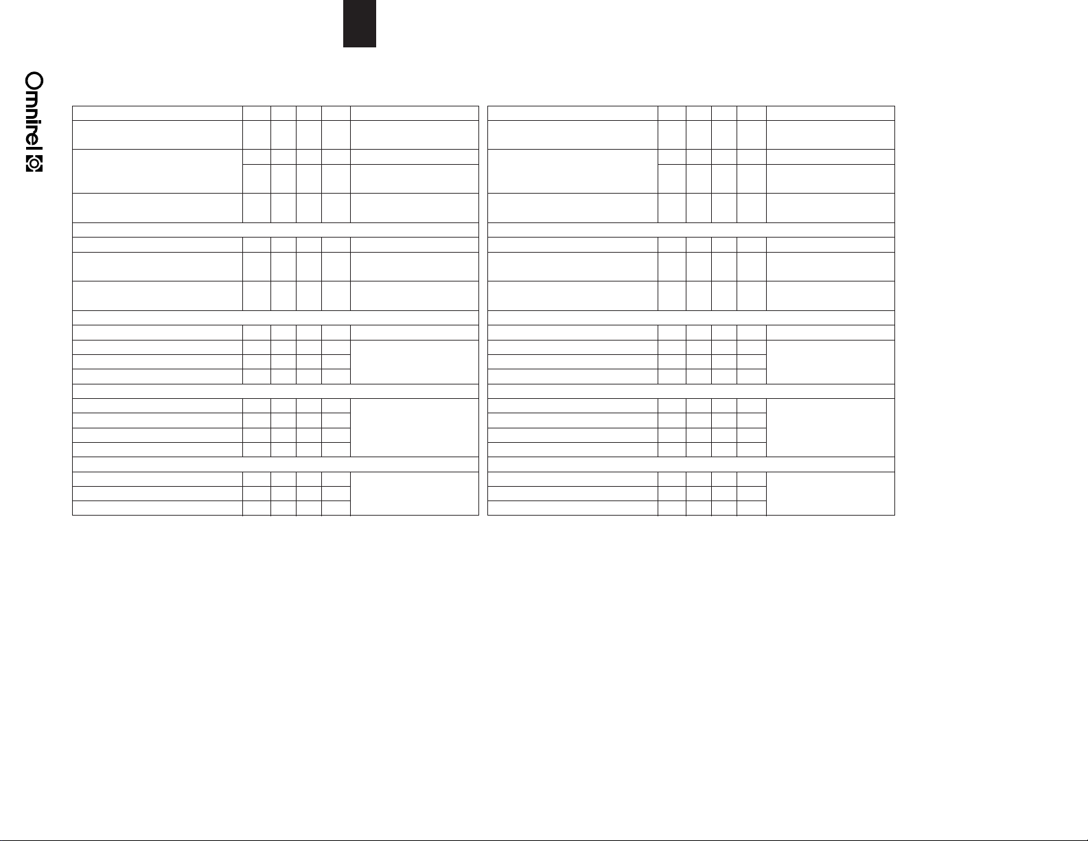
PRELIMINARY DATA: OM6517SA
IGBT CHARACTERISTICS
Parameter - OFF Min. Typ. Max. Units Test Conditions
V
(BR)CES
I
CES
I
GES
Parameter - ON
V
GE(th)
V
CE(sat)
V
CE(sat)
Dynamic
g
fs
C
ies
C
oes
C
res
Switching-Resistive Load
T
d(on)
t
r
T
d(off)
t
f
Switching-Inductive Load
T
d(off)
t
f
E
off
Collector Emitter 1000 V VCE= 0
Breakdown Voltage I
= 250 µA
C
Zero Gate Voltage 0.25 mA VCE= Max. Rat., VGE= 0
Drain Current 1.0 mA V
= 0.8 Max. Rat., VGE= 0
CE
T
= 125°C
C
Gate Emitter Leakage ±100 nA VGE= ±20 V
Current V
CE
= 0 V
Gate Threshold Voltage 4.5 6.5 V VCE= VGE, IC= 1 mA
Collector Emitter 3.0 V VGE= 15 V, IC= 15 A
Saturation Voltage T
= 25°C
C
Collector Emitter 4.0 4.5 V VGE= 15 V, IC= 15 A
Saturation Voltage T
= 125°C
C
Forward Transductance 5.5 S VCE= 20 V, IC= 15 A
Input Capacitance 2000 pF VGE= 0
Output Capacitance 160 pF VCE= 25 V
Reverse Transfer Capacitance 65 pF f = 1 mHz
Turn-On Time 50 nS VCC= 600 V, IC= 15 A
Rise Time 200 nS VGE= 15 V, Rg= 3.3 ,
Turn-Off Delay Time 200 nS Tj= 125°C
Fall Time 300 nS
Turn-Off Delay Time 200 nS V
= 600 V, IC= 15 A
CEclamp
Fall Time 200 nS VGE= 15 V, Rg= 3.3
Turn-Off Losses 1.5 mWs L = 1 mH, Tj= 125°C
PRELIMINARY DATA: OM6526SA
IGBT CHARACTERISTICS
Parameter - OFF Min. Typ. Max. Units Test Conditions
V
Collector Emitter 1000 V VCE= 0
(BR)CES
Breakdown Voltage I
I
Zero Gate Voltage 150 µA VCE= Max. Rat., VGE= 0
CES
Drain Current 700 µA V
I
Gate Emitter Leakage ±100 nA VGE= ±20 V
GES
Current V
Parameter - ON
V
Gate Threshold Voltage 4.5 6.5 V VCE= VGE, IC= 700 µA
GE(th)
V
Collector Emitter 3.0 V VGE= 15 V, IC= 10 A
CE(sat)
Saturation Voltage T
V
Collector Emitter 4.0 4.5 V VGE= 15 V, IC= 10 A
CE(sat)
Saturation Voltage T
Dynamic
g
Forward Transductance 3.5 S VCE= 20 V, IC= 10 A
fs
C
Input Capacitance 1300 pF VGE= 0
ies
C
Output Capacitance 100 pF VCE= 25 V
oes
C
Reverse Transfer Capacitance 50 pF f = 1 mHz
res
Switching-Resistive Load
T
Turn-On Time 50 nS VCC= 600 V, IC= 10 A
d(on)
t
Rise Time 200 nS VGE= 15 V, Rg= 3.3 ,
r
T
Turn-Off Delay Time 200 nS Tj= 125°C
d(off)
t
Fall Time 300 nS
f
Switching-Inductive Load
T
Turn-Off Delay Time 200 nS V
d(off)
t
Fall Time 200 nS VGE= 15 V, Rg= 3.3
f
E
Turn-Off Losses 1.1 mWs L = 1 mH, Tj= 125°C
off
= 150 µA
C
= 0.8 Max. Rat., VGE= 0
CE
T
= 125°C
C
= 0 V
CE
= 25°C
C
= 125°C
C
= 600 V, IC= 10 A
CEclamp
 Loading...