


1.5 AMP HIGH VOLTAGE POSITIVE
ADJUSTABLE REGULATOR
Three T erminal, High V oltage, Precision
Adjustable Positive Voltage Regulator In
Hermetic JEDEC TO-257AA
FEATURES
• Similar To Industry Standard LT117AHV
• Adjustable Output Voltage
• Built In Thermal Overload Protection
• Short Circuit Current Limiting
• Available In Isolated and Non-Isolated Package
• Maximum Output Voltage Tolerance Is Guaranteed To ±1%
• Available Hi-Rel Screened
OM7620ST
DESCRIPTION
This three terminal positive regulator is supplied in a hermetically sealed metal
package whose outline is similar to the industry standard TO-220 plastic package. All
protective features are designed into the circuit, including thermal shutdown, current
limiting, and safe-area control. With heat sinking, these devices can deliver up to 1.5
amps of output current. The unit also features output voltages that can be fixed from
1.2 volts to 57 volts using external resistors.
ABSOLUTE MAXIMUM RATINGS @ 25°C
Power Dissipation (Pd) (Internally Limited) .................................20 W
Input - Output Voltage Differential.........................................60 V
Operating Junction Temperature Range........................- 55°C to + 150°C
Storage Temperature Range .................................- 65°C to + 150°C
Lead Temperature (Soldering 10 seconds)................................300°C
Thermal Resistance:
qJC(Isolated) .....................................................4.2°C/W
qJC(Non-Isolated).................................................3.5°C/W
qJA...............................................................42°C/W
Maximum Output Current................................................1.5 A
3.3
4 11 R0
3.3 - 169
OM7620ST
3.3
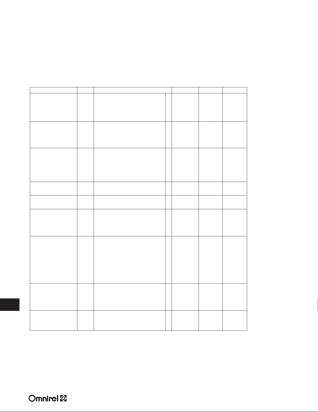
ELECTRICAL CHARACTERISTICS
-55°C TA 125°C, IL= 8mA (unless otherwise specified)
Parameter Symbol Test Conditions Min. Max. Unit
Reference Voltage V
Line Regulation R
REF
LINE
(Note 1) 3.3V V
Load Regulation R
LOAD
(Note 1) V
Thermal Regulation V
Ripple Rejection R
RTH
N
(Note 2) C
Adjustment Pin Current I
Adjustment Pin ³I
Adj
Adj
Current Change V
Miminum Load Current I
Current Limit I
Lmin
CL
(Note 2) V
V
= 3.0V, TA= 25°C 1.238 1.262
DIFF
V
= 3.3V • 1.225 1.270 V
DIFF
V
= 40V • 1.225 1.270
DIFF
V
= 60V • 1.225 1.270
DIFF
3.0V V
40V V
V
DIFF
V
DIFF
DIFF
DIFF
40V V
40V, V
DIFF
60V, V
DIFF
OUT
40V, V
OUT
60V, V
= V
, TA= 25°C -4.5 4.5
ref
= V
OUT
ref
= V
, TA= 25°C -5 5
ref
= V
OUT
ref
• -9 9 mV
• -10 10
= 3.0V, 10mA IL 1.5A, TA= 25°C -15 15
= 3.3V, 10mA IL 1.5A • -15 15 mV
DIFF
= 40V, 10mA IL 300mA, TA= 25°C -15 15
V
= 40V, 10mA IL 195mA • -15 15
DIFF
V
= 60V, 10mA IL 30mA • -15 15
DIFF
VIN= 14.6V, IL= 1.5A -5 5 mV
P
= 20 Watts, t = 20 ms, TA= 25°C
d
f = 120 Hz, V
= 10 µF, I
Adj
V
= 3.0V, TA= 25°C 100
DIFF
V
DIFF
V
V
V
= 3.0V, 10mA IL 1.5A, TA= 25°C -5 5
DIFF
= 3.3V, 10mA IL 1.5A • -5 5
DIFF
V
= 40V, 10mA IL 300mA, TA= 25°C -5 5
DIFF
V
= 40V, 10mA IL 195mA • -5 5 µA
DIFF
3.0V V
DIFF
3.3V V
3.3V V
V
= 3.0V, V
DIFF
OUT
V
= 3.3V, V
DIFF
V
= 40V, V
DIFF
V
= 60V, V
DIFF
V
= 40V, TA= 25°C 0.3 1.5 A
DIFF
V
= 60V, TA= 25°C 0.05 0.50
DIFF
OUT
OUT
= V
ref
= 100 mA
• 66 dB
= 3.3V • 100 µA
= 40V • 100
DIFF
= 60V • 100
DIFF
40V, TA= 25°C -5 5
40V • -5 5
DIFF
60V • -5 5
DIFF
= 1.4V (forced), TA= 25°C 5
= 1.4V (forced) • 5mA
OUT
= 1.4V (forced) • 5
OUT
= 1.4V (forced) • 7
OUT
= 5V • 1.5 3.5
DIFF
Notes:
1. Load and Line Regulation are specified at a constant junction temperature. Pulse testing with low duty cycle is used.
Changes in output voltage due to heating effects must be taken into account separately.
2. If not tested, shall be guaranteed to the specified limits.
3. The • denotes the specifications which apply over the full operating temperature range.
3.3 - 170

0.2
0
-0.2
-0.4
-0.6
-0.8
-1.0
-75 -50
-25
0255075
100
125
150
0.4
-75 -50
-25
0255075
100
125
150
65
60
55
50
45
40
35
70
1.260
1.250
1.240
1.230
1.220
-75
-50 -25 0 25 50
75
100
125 150
3.0
2.5
2.0
1.5
1.0
-75 -50 -25 0
25 50 75
100
125
150
5.0
4.5
4.0
3.5
3.0
2.5
2.0
1.5
1.0
0.5
0
0
10
20 30
40
TYPICAL APPLICATIONS
OM7620ST
LOAD REGULATION
0.4
0.2
0
-0.2
-0.4
-0.6
VI= 15V
VO= 10V
-0.8
, Output Voltage Change (%)
O
-1.0
³V
-75 -50 -25 0 25 50 75 100 125 150
TJ, Junction Temperature (C°)
ADJUSTMENT PIN CURRENT
70
65
60
55
50
45
40
, Adjustment Pin Current (µA)
35
Adj
I
-75 -50 -25 0 25 50 75 100 125 150
TJ, Junction Temperature (C°)
TEMPERATURE STABILITY
1.260
1.250
1.240
1.230
, Reference Voltage (V)
ref
V
1.220
-75 -50 -25 0 25 50 75 100 125 150
T
, Junction Temperature (C°)
J
IL= 1.5A
IL= 0.5A
CURRENT LIMIT
4
3
TJ= 25°C
2
TJ= 55°C
TJ= 150°C
1
, Output Current (A)
O
I
0
010203040
V
- VO, Input - Output Voltage Differential (Vdc)
I
)
dc
DROPOUT VOLTAGE
3.0
³VO= 100mV
2.5
IL= 1.5A
2.0
1.5
1.0
IL= 20mA
, Input - Output Voltage Differential (V
O
-75 -50 -25 0 25 50 75 100 125 150
- V
I
V
TJ, Junction Temperature (C°)
IL= 200mA
MINIMUM OPERATING CURRENT
5.0
4.5
4.0
3.5
3.0
2.5
2.0
1.5
1.0
0.5
, Quiescent Current (mA)
B
I
TJ= 25°C
TJ= 150°C
0
010203040
- VO, Input - Output Voltage Differential (Vdc)
V
I
IL= 1.0A
IL= 500mA
TJ= 55°C
3.3
*CINis required if regulator is located an
appreciable distance from power supply filter.
** C
is not needed for stability, however it does
o
improve transient response.
V
= 1.25 V (1 + )+ I
OUT
Since I
is controlled to less than 100 µA,
Adj
the error associated with this term is negligible
in most applications.
STANDARD APPLICATION
V
IN
CIN*
R2
R1
Adj
R2
3.3 - 171
0.1 µF
OM7620ST
I
Adj
Adjust
R2
V
OUT
R1
240
Co**
1.0 µF

205 Crawford Street, Leominster, MA 01453 USA (508) 534-5776 FAX (508) 537-4246
OM7620ST
.430
.410
.200
.190
.038 MAX.
.005
.120 TYP.
.537
.527
.665
.645
.420
.410
.150
.140
.750
.500
.100 TYP.
.035
.025
.045
.035
TYPICAL APPLICATIONS
ADJUSTABLE CURRENT LIMITER
+25V
OM7620ST
V
IN
Adjust
* To provide current limiting of IOto the
system ground, the source of the FET
must be tied to a negative voltage
below -1.25 V.
V
REF
R2 R1
I
DSS
VO < BV
I
As shown 0< IO< 1 A
Lmin
– I
DSS
< IO< 1.5 A
DSS
+ 1.25 V + V
=
V
V
REF
I
Omax + IDSS
SS
OUT
R1 V
1.25
R2
100
SLOW TURN-ON CURRENT CURRENT REGULATOR
V
IN
OM7620ST
Adjust
R2
MPS2907
V
OUT
240
50 K
5 V ELECTRONIC SHUT DOWN REGULATOR
D
I
O
O
V
V
IN
1N4002
IN
OM7620ST
Adjust
720
2N5640
V
ss*
IN4001
D
protects the device during an input short circuit.
1
V
IN
OM7620ST
Adjust
I
+
10 µF
OUT
1
120
Minimum V
V
OUT
I
Adj
(V
) + I
REF
Adj
= @
R1 R1
10mA I
OUT
V
OUT
1.5 A
R1 I
1.0µF
MPS2222
1 K
OUT
1.25 V
= 1.25 V
OUT
TTL
Control
3.3
MECHANICAL OUTLINE
NOTES
• Case is metal/hermetically sealed
• Isolated Tab
CONNECTION DIAGRAM
Tab
123
Isolated Non-Isolated
Front View Front View
Pin 1 - Adjust Pin 1 - Adjust
Pin 2 - Output Pin 2 - Output
Pin 3 - Input Pin 3 - Input
Tab - Isolated Tab - Output
 Loading...