


ISOLATED HERMETIC TO-257AA
ADJUST ABLE V OL T A GE REGULA TOR
Three T erminal, Adjustable V oltage, 3.0 Amp
Precision Positive Regulator In A Hermetic
JEDEC TO-257AA P ackage
FEA TURES
• Isolated Hermetic Package, JEDEC TO-257AA Outline
• Reference Voltages Set To ±2% (±1% Available)
• Built-In Thermal Overload Protection
• Short Circuit Current Limiting
• Product Is Available Screened To MIL-STD-883
• Similar To Industry Standard P/N LM150A
DESCRIPTION
These three terminal positive regulators are supplied in a hermetically sealed metal
package whose outline is similar to the industry standard TO-220 plastic package. All
protective features are designed into the circuit, including thermal shutdown, current
limiting and safe-area control. With heat sinking, they can deliver over 3.0 amps of
output current. These units feature 2% initial voltage tolerance, 0.3% load regulation
and 0.01% line regulation.
OM7604ST
ABSOLUTE MAXIMUM RATINGS @ 25°C
Input Voltage ..................................................................+35V
Operating Junction Temperature Range.............................-55°C to +150°C
Storage Temperature Range .........................................-65° to +150°C
Typical Power/Thermal Characteristics:
Note: For ±1% device, add letter "A" in front of part number (e.g. OMA 7604ST).
4 11 R4
Supersedes 1 07 R3
Rated Power @ 25°C
TC........................................................................25W
TA..........................................................................3W
Thermal Resistance
qJC....................................................................4.2°C/W
qJA.....................................................................42°C/W
3.3 - 141
3.3
OM7604ST
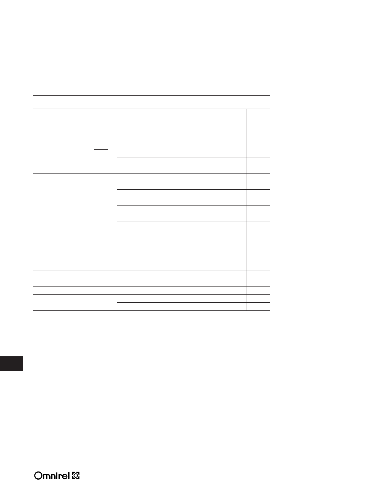
ELECTRICAL CHARACTERISTICS -55°C T
Test Symbol Conditions Limits Unit
Reference Voltage V
Line Regulation ³V
(Note 2) ³V
Load Regulation ³V
(Note 2) ³I
REF
OUT
IN
OUT
OUT
Thermal Regulation 20ms pulse, T
Ripple Rejection ³V
(Note 3) ³V
Adjust Pin Current I
Adjust Pin ³I
IN
REF
Adj
Adj
Current Change 3.0V (V
Miminum Load Current I
Current Limit I
MIN
CL
I
= 10mA 1.20 1.30 V
OUT
T
= 25°C
A
3.0V (V
10mA I
3.0V (V
I
= 10mA, TJ= 25°C
OUT
3.0V (V
I
= 10mA
OUT
10mA I
V
5.0A, TJ= 25°C
OUT
10mA I
V
5.0A
OUT
10mA I
V
5.0A, TJ= 25°C
OUT
10mA I
V
5.0A
OUT
V
= 10V, f = 120Hz 66 dB
OUT
C
= 10µF
ADJ
10mA I
(V
IN - VOUT
(V
IN - VOUT
(V
IN - VOUT
) 35V, P 30W 1.20 1.30 V
IN - VOUT
3.0A (Note 2)
OUT
) 35V, 0.01 %/V
IN - VOUT
) 35V, 0.05 %/
IN - VOUT
3.0A, 17.5 mV
OUT
3.0A, 50 mV
OUT
3.0A, 0.35 %
OUT
3.0A, 1.0 %
OUT
=25°C 0.01 %/W
A
3.0A, I
OUT
IN - VOUT
= 10mA 5.0 µA
OUT
) 35V
) = 35V 5.0 mA
) 10V 3.0 A
) = 30V 0.3 A
125°C (Note 1) unless otherwise specified
A
Min. Max.
100 µA
3.3
Notes:
1. Unless otherwise specified, these specifications apply for (VIN- V
dissipation is internally limited, these characteristics are applicable for power dissipation up to 30W.
) = 5.0V and I
OUT
= 1.5A. Although power
OUT
2. Regulation is measured at a constant junction temperature using a pulse technique. Changes in output voltage
due to heating effects are covered under the specification for thermal regulation.
3. Guaranteed if not tested to the limits specified.
3.3 - 142

TYPICAL PERFORMANCE CHARACTERISTICS
Voltage Change (Percent)
1.0
0
0.1
0.2
0.3
0.4
0.5
-75
-50 -25 0 25 50 75 100125150
Temperature (°C)
Load Regulation Current Limit
Adjustment Current (µA)
65
60
55
50
45
40
35
30
-75 -25 25 75 125
Temperature (°C)
Adjustment Current
Dropout Voltage
Reference Voltage (V)
1.27
1.26
1.25
1.24
1.23
-50 -25 -0 25 50 75 100 125 150
Temperature (°C)
Temperature Stability
Minimum I
OUT
Current (mA)
5
4
3
2
1
0
0 5 10 15 20 25 30 35 40
Input-Output Diffential(V)
Minimum Operating Current
Ripple Rejection (dB)
100
80
60
40
20
0
0
5101520253035
Output Voltage (V)
Ripple Rejection
Ripple Rejection (dB)
100
80
60
40
20
0
10 100 1k 10k 100k 1M
Frequency (Hz)
Ripple Rejection
Ripple Rejection (dB)
80
70
60
50
40
0.1 1 10
Output Current (A)
Ripple Rejection
Output Impedance (Ohms)
10
1
0.1
0.01
0.001
0.0001
10
100 1k 10k 100k 1M
Frequency (Hz)
Output Impedance
1.5
1
0.5
0
-0.5
-1
1
0.5
0
0 10203040
Time (µs)
Line Transient Response
1.5
1
0.5
0
-0.5
-1
-1.5
1.5
1
0.5
0
0 10203040
Time (µs)
Load Transient Response
Input Voltage
Change(V)
Output Voltage
(Deviation (V)
Load
Current (A)
Output Voltage
Deviation (V)
C
ADJ
= 10µF
VIN - V
OUT
= 5V
V
OUT
= 500mA
f = 120Hz
T
J
= 25°C
VIN = 15V
V
OUT
= 10V
f = 120Hz
T
CASE
= 25°C
VIN = 15V, V
OUT
= 10V
Preload = 100mA
T
J
= 25°C
VIN = 15V
V
OUT
= 10V
I
OUT
= 500mA
V
OUT
= 10V
I
OUT
= 50mA
TJ = 25°C
VIN = 15V
V
OUT
= 10V
I
OUT
= 500mA
C
ADJ
= 0
C
ADJ
= 10µF
C
ADJ
= 0
C
ADJ
= 10µF
C
OUT
= 10µF
C
ADJ
= 0
C
OUT
= 0
C
OUT
= 1µF
C
OUT
= 0
C
ADJ
= 10µF
C
ADJ
= 0
C
ADJ
= 10µF
C
ADJ
= 0
C
OUT
= 1µF C
ADJ
= 10µF
C
OUT
= 0 C
ADJ
= 0
Output Current (A)
6
4
2
0
0 5 10 15 20 25 30 35
Input-Output Differential (V)
I
OUT
= 3A
TJ = 150°C
TJ = 25°C
TJ = -55°C
TJ = 150°C
TJ = 25°C
TJ = -55°C
Input-Output Differential (V)
3
2.5
2
1.5
1
0.5
-75 -25 25 75 125
Temperature (°C)
∆V
OUT
= 100 mV
I
OUT
= 3 A
I
OUT
= 2 A
I
OUT
= 20 mA
OM7604ST
3.3
3.3 - 143

205 Crawford Street, Leominster, MA 01453 USA (508) 534-5776 FAX (508) 537-4246
OM7604ST
.430
.410
.200
.190
.038 MAX.
.005
.120 TYP.
.537
.527
.665
.645
.420
.410
.150
.140
.750
.500
.100 TYP.
.035
.025
.045
.035
V
OUT
V
IN
V
IN
Adj
LT 301A
25
1k
25
121
365
100pF
5µF
++-
-
3
2
7
6
5V
RET
R
L
R
p
Return
1
8
(Max Drop 300mV)
V
OUT
V
IN
Adj
1K
500
0.5
V
OUT
V
OUT
V
IN
Adj
C1*
1µF
C2
R1
240
R2
5k
1µF
+
+
+
+
+
V
OUT
= 1.25V(1 + )
R2
R1
*Needed if device is far
from filter capacitors.
+
l
+
l
Optional - improves
transient response.
5V
*C1 improves ripple rejection,
X
C
should be small compared to R2.
1µF
10µf*
V
OUT
V
IN
V
IN
Adj
R2
365
1%
R1
121
1%
+
C1
1.2 - 2.5V Adjustable Regulator Improving Ripple Rejection Adjustable Current Limiter
Remote Sensing
4
V
IN
V
OUT
V
IN
V
IN
Adj
LT 1001
3
2
2.5V
LT 1009
4.99k
1%
15k
1%
2k
4
6
7
2k
+10V
Precision High Current Reference
+
-
TYPICAL APPLICATIONS
MECHANICAL OUTLINE PIN CONNECTION
3.3
NOTES
• Case is metal/hermetically sealed
• Isolated Tab
123
Front View
Pin 1: Adjust
Pin 2: V
Pin 3: V
Tab: Isolated
OUT
IN
Tab
 Loading...