


OMNIREL JANTXV2N7227, JANTXV2N7225, JANTXV2N7224, JANTX2N7227, JANTX2N7225 Datasheet
...
2N7224, JANTX2N7224, JANTXV2N7224 2N7227, JANTX2N7227, JANTXV2N7227
2N7225, JANTX2N7225, JANTXV2N7225 2N7228, JANTX2N7228, JANTXV2N7228
JANTX, JANTXV POWER MOSFET IN TO-254AA PACKAGE,
QUALIFIED TO MIL-PRF-19500/592
100V Thru 500V, Up to 34A, N-Channel,
MOSFET Power Transistor, Repetitive Avalanche Rated
FEATURES
• Repetitive Avalanche Rating
• Isolated and Hermetically Sealed
• Low R
• Ease of Paralleling
• Ceramic Feedthroughs
• Qualified to MIL-PRF-19500
DESCRIPTION
This hermetically packaged QPL product features the latest advanced MOSFET and packaging technology. I t i s
ideally suited for Military requirements where small size, high performance and high reliability are required, and in
applications such as switching power supplies, motor controls, inverters, choppers, audio amplifiers and high energy
pulse circuits.
DS(on)
PRIMARY ELECTRICAL CHARACTERISTICS @ TC= 25°C
PART NUMBER V
V olts R
DS,
2N7224 100 .070 34
2N7225 200 .100 27.4
2N7227 400 .315 14
2N7228 500 .415 12
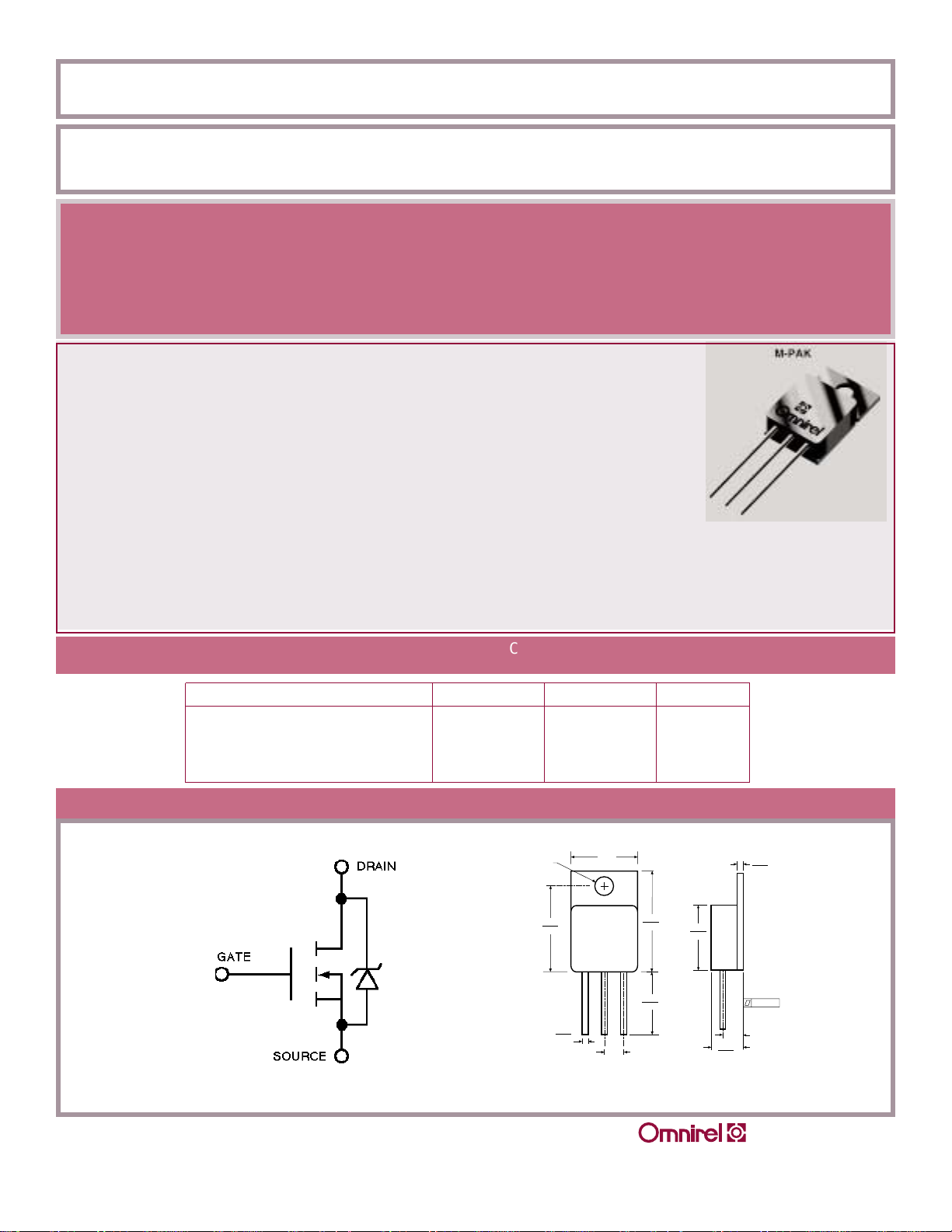
.144 DIA.
.685
.665
.045
.035
DS(on)
MECHANICAL OUTLINESCHEMATIC
.545
.535
123
.800
.790
.550
.510
.150 TYP.
I
D,
Amps
.550
.530
.260
.249
.050
.040
.005
.150 TYP.
Pin Connection
Pin 1: Drain
Pin 2: Source
Pin 3: Gate
4 11 R0
3.1 - 1
2N7224, JANTX2N7224, JANTXV2N7224 2N7227, JANTX2N7227, JANTXV2N7227
2N7225, JANTX2N7225, JANTXV2N7225 2N7228, JANTX2N7228, JANTXV2N7228
ABSOLUTE MAXIMUM RATINGS (TC= 25°C unless otherwise noted
Parameter JANTXV, JANTX, 2N7224 Units
ID @ V
ID @ V
I
= 10V, TC= 25°C Continuous Drain Current 34 A
GS
= 10V, TC= 100°C Continuous Drain Current 21 A
DM
GS
Pulsed Drain Current
1
PD@ TC= 25°C Maximum Power Dissipation 150 W
Linear Derating Factor 1. 2 W/°C
V
GS
E
AS
I
AR
E
AR
J Operating Junction
T
Gate-Source Voltage ± 2 0 V
Single Pulse Avalanche Energy
Avalanche Current
1
Repetitive Avalanche Energy
2
1
TSTG Storage Temperature Range
Lead Temperature 300(.06 from case for 10 sec) °C
ELECTRICAL CHARACTERISTICS @ TJ = 25°C (Unless Otherwise Specified)
Parameter Min. Typ. Max. Units Test Conditions
Drain-Source 100 V VGS= 0V, ID=1.0 mA,
BV
DSS
Breakdown Voltage
R
Static Drain-to-Source - ----- 0.07 VGS= 10 V, ID= 21 A
DS(on)
On-State Resistance ------ 0.081 VGS= 10 V, ID= 34 A
V
Gate Threshold Voltage 2. 0 --- 4.0 V V
GS(th)
I
Zero Gate Voltage Drain ------ 25
DSS
Current ------ 250 V
I
Gate -to-Source Leakage Forward ------ 100 nA VGS= 20 V
GSS
I
Gate -to-Source Leakage Reverse ------ -100 nA VGS= -20 V
GSS
Q
On-state Gate Charge ------ 125 n C VGS= 10 V, ID= 34A
G(on)
Q
Gate-to-Source Charge ------22nCVDS= 50 V
GS
Q
Gate-to-Drain (“Miller”) Charge - ----- 65 n C See note 4
Gd
t
Turn-On Delay Time ------35nsVDD= 50 V, ID= 21A, RG = 2.35
D(on)
t
Rise Time ------ 190 ns See note 4
r
t
Turn-Off Delay Time ------ 170 n s
D(off)
t
Fall Time ------ 130 n s
r
µA
136 A
4
150
34
15
4
4
mJ
mJ
-55 to 150 °C
3
3
= VGS, ID= 250 µA
DS
VDS= 80 V, VGS= 0V
= 80 V, VGS= 0V, TJ= 125°C
DS
A
Source-Drain Diode Ratings and Characteristics
Parameter Min. Typ. Max. Units Test Conditions
Diode Forward Voltage ------ 1.8 V TJ= 25°C, IS= 34A 3, VGS= 0 V
V
SD
t
Reverse Recovery Time ------ 500 n s TJ= 25°C, IF= 34A,d i/dt<100A/µs
trr
Thermal Resistance
Parameter Min. Typ. Max. Units Test Conditions
R
Junction-to-Case ------ 0.83 Mounting surface flat,
thJC
R
Case-to-sink --- 0.21 - -- °C/W smooth, and greased
thCS
R
Junction-to-Ambient ------ 48 Typical socket mount
thJA
1. Repetitive Rating: Pulse width limited by maximum junction temperature.
2. @V
3. Pulse width <
= 25V, Starting TJ= 25°C, L > 200 µH, RG = 25 , Peak IL = 34A
DD
300 µs; Duty Cycle < 2%
4. See MIL-S-19500/592
205 Crawford Street, Leominster, MA 01453 USA (508) 534-5776 FAX (508) 537-4246
 Loading...