

3.1 - 1
3.1
(COTS) COMMERCIAL OFF-THE-SHELF
POWER MOSFET IN A TO-254AA PACKAGE
FEATURES
• Isolated Hermetic Metal Package
• Fast Switching
• Low R
DS(on)
• Standard Off-The-Shelf
DESCRIPTION
This series of hermetically packaged products feature the latest advanced MOSFET
and packaging technology. They are ideally suited for Military requirements where
small size, high performance and high reliability are required, and in applications
such as switching power supplies, motor controls, inverters, choppers, audio
amplifiers and high energy pulse circuits.
MAXIMUM RATINGS @ 25
°
C
COM350A
COM450A
COM150A
COM250A
100V Thru 500V, U p To 25 Amp, N-Channel
MOSFET In Hermetic Metal Package
8 09 R0
PART NUMBER V
DS
R
DS(on)
I
D
COM150A 100 V .070 25 A
COM250A 200 V .100 20 A
COM350A 400 V .32 12 A
COM450A 500 V .42 10 A
SCHEMATIC POWER RATING
3.1 - 2
COM150A - COM450A
3.1
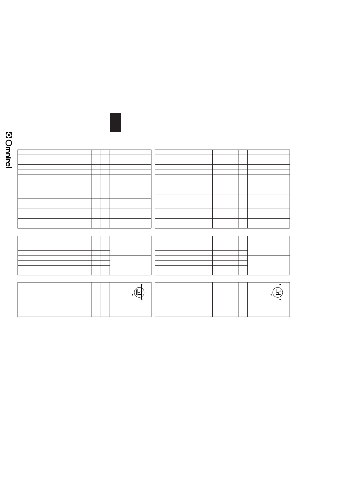
ELECTRICAL CHARACTERISTICS: (T
C
= 25°C unless otherwise noted) ELECTRICAL CHARACTERISTICS: (TC= 25°C unless otherwise noted)
STATIC P/N COM150A STATIC P/N COM250A
Parameter Min. Typ. Max. Units Test Conditions Parameter Min. Typ. Max. Units Test Conditions
BV
DSS
Drain-Source Breakdown
100 V
VGS= 0,BV
DSS
Drain-Source Breakdown
200 V
VGS= 0,
Voltage I
D
= 250 mA Voltage ID= 250 mA
V
GS(th)
Gate-Threshold Voltage 2. 0 4. 0 V VDS= VGS, ID= 250 mAV
GS(th)
Gate-Threshold Voltage 2. 0 4. 0 V VDS= VGS, ID= 250 mA
I
GSSF
Gate-Body Leakage Forward 100 nA VGS= +20 V I
GSSF
Gate-Body Leakage Forward 100 nA VGS= + 20 V
I
GSSR
Gate-Body Leakage Reverse - 1 0 0 nA VGS= -20 V I
GSSR
Gate-Body Leakage Reverse -100 nA VGS= - 20 V
I
DSS
Zero Gate Voltage Drain 0. 1 0.25 m A VDS= Max. Rat., VGS= 0 I
DSS
Zero Gate Voltage Drain 0. 1 0.25 m A VDS= Max. Rat., VGS= 0
Current
0.2 1.0 m A
V
DS
= 0.8 Max. Rat., VGS= 0, Current
0.2 1.0 m A
VDS= 0.8 Max. Rat., VGS= 0,
T
C
= 125° C TC= 125° C
I
D(on)
On-State Drain Current
1
35 A VDS 2 V
DS(on)
, VGS= 10 V I
D(on)
On-State Drain Current
1
30 A VDS 2 V
DS(on)
, VGS= 10 V
V
DS(on)
Static Drain-Source On-State
1.1 1.3 V V
GS
= 10 V, ID= 20 A
V
DS(on)
Static Drain-Source On-State
1.36 1.60 V V
GS
= 10 V, ID= 16 A
Voltage
1
Voltage
1
R
DS(on)
Static Drain-Source On-State
0.55 0.07 V
GS
= 10 V, ID= 20 A
R
DS(on)
Static Drain-Source On-State
.085 .100 V
GS
= 10 V, ID= 16 A
Resistance
1
Resistance
1
R
DS(on)
Static Drain-Source On-State
1.0 0.12
VGS= 10 V, ID= 20 A, R
DS(on)
Static Drain-Source On-State
0.15 0.18
VGS= 10 V, ID= 16 A,
Resistance
1
TC= 125 C Resistance
1
TC= 125 C
DYNAMIC DYNAMIC
gfsForward Transductance
1
9.0 S (W) VDS 2 V
DS(on)
, ID= 20 A gfsForward Transductance
1
10.0 S (W ) VDS 2 V
DS(on)
, ID= 16 A
C
iss
Input Capacitance 2700 pF VGS= 0 C
iss
Input Capacitance 2400 pF VGS= 0
C
oss
Output Capacitance 1300 pF VDS= 25 V C
oss
Output Capacitance 600 pF VDS= 25 V
C
rss
Reverse Transfer Capacitance 470 pF f = 1 MHz C
rss
Reverse Transfer Capacitance 250 pF f = 1 MHz
t
d(on)
Turn-On Delay Time 28 ns VDD= 30 V, ID@ 20 A t
d(on)
Turn-On Delay Time 25 ns VDD= 75 V, ID@ 16 A
t
r
Rise Time 45 ns Rg= 5.0 W , VG= 10V trRise Time 60 ns Rg= 5.0 W ,VGS= 10V
t
d(off)
Turn-Off Delay Time 100 ns t
d(off)
Turn-Off Delay Time 85 ns
t
f
Fall Time 50 ns tfFall Time 38 ns
BODY-DRAIN DIODE RATINGS AND CHARACTERISTICS BODY-DRAIN DIODE RATINGS AND CHARACTERISTICS
ISContinuous Source Current
- 40A
Modified MOSPOWER I
S
Continuous Source Current
- 30A
Modified MOSPOWER
(Body Diode) symbol showing (Body Diode) symbol showing
ISMSource Current
1
- 160 A
the integral P-N I
SM
Source Current
1
- 120 A
the integral P-N
(Body Diode) Junction rectifier.
(Body Diode) Junction rectifier.
VSDDiode Forward Voltage
1
- 2.5V TC= 25 C , IS= -40 A, VGS= 0 VSDDiode Forward Voltage
1
- 2VTC= 25 C , IS= -30 A, VGS= 0
t
rr
Reverse Recovery Time 400 ns
T
J
= 150 C , IF= IS,
t
rr
Reverse Recovery Time 350 ns
T
J
= 150 C , IF= IS,
dl
F
/ds = 100 A/ms dlF/ds = 100 A/ms
1 Pulse Test: Pulse Width 300msec, Duty Cycle 2%. 1 Pulse Test: Pulse Width 300msec, Duty Cycle 2%.
(MOSFET switching times are
essentially independent of
operating temperature.)
(MOSFET switching times are
essentially independent of
operating temperature.)
G
D
S
G
D
S
(W )
(W )

ELECTRICAL CHARACTERISTICS: (T
C
= 25°C unless otherwise noted) ELECTRICAL CHARACTERISTICS: (TC= 25°C unless otherwise noted)
STATIC P/N COM350A STATIC P/N COM450A
Parameter Min. Typ. Max. Units Test Conditions Parameter Min. Typ. Max. Units Test Conditions
BV
DSS
Drain-Source Breakdown
400 V
VGS= 0,BV
DSS
Drain-Source Breakdown
500 V
VGS= 0,
Voltage I
D
= 250 mA Voltage ID= 250 mA
V
GS(th)
Gate-Threshold Voltage 2. 0 4. 0 V VDS= VGS, ID= 250 mAV
GS(th)
Gate-Threshold Voltage 2. 0 4. 0 V VDS= VGS, ID= 250 mA
I
GSSF
Gate-Body Leakage Forward 100 nA VGS= +20 V I
GSSF
Gate-Body Leakage Forward 100 nA VGS= +20 V
I
GSSR
Gate-Body Leakage Reverse - 1 0 0 nA VGS= - 20 V I
GSSR
Gate-Body Leakage Reverse - 1 0 0 nA VGS= - 20 V
I
DSS
Zero Gate Voltage Drain 0. 1 0.25 m A VDS= Max. Rat., VGS= 0 I
DSS
Zero Gate Voltage Drain 0. 1 0.25 m A VDS= Max. Rat., VGS= 0
Current
0.2 1.0 m A
V
DS
= 0.8 Max. Rat., VGS= 0, Current
0.2 1.0 m A
VDS= 0.8 Max. Rat., VGS= 0,
T
C
= 125° C TC= 125° C
I
D(on)
On-State Drain Current
1
15 A VDS 2 V
DS(on)
, VGS= 10 V I
D(on)
On-State Drain Current
1
13 A VDS 2 V
DS(on)
, VGS= 10 V
V
DS(on)
Static Drain-Source On-State
2.0 2.64 V V
GS
= 10 V, ID= 8.0 A
V
DS(on)
Static Drain-Source On-State
2.1 2.94 V V
GS
= 10 V, ID= 7.0 A
Voltage
1
Voltage
1
R
DS(on)
Static Drain-Source On-State
0.25 .32 V
GS
= 10 V, ID= 8.0 A
R
DS(on)
Static Drain-Source On-State
0.3 0.42 V
GS
= 10 V, ID= 7.0 A
Resistance
1
Resistance
1
R
DS(on)
Static Drain-Source On-State
0.51 0.67
VGS= 10 V, ID= 8.0 A, R
DS(on)
Static Drain-Source On-State
0.67 0.89
VGS= 10 V, ID= 7.0 A,
Resistance
1
TC= 125 C Resistance
1
TC= 125 C
DYNAMIC DYNAMIC
gfsForward Transductance
1
6.0 S (W) VDS 2 V
DS(on)
, ID= 8.0 A gfsForward Transductance
1
6.0 S (W) VDS 2 V
DS(on)
, ID= 7.0 A
C
iss
Input Capacitance 2900 pF VGS= 0 C
iss
Input Capacitance 2600 pF VGS= 0
C
oss
Output Capacitance 450 pF VDS= 25 V C
oss
Output Capacitance 280 pF VDS= 25 V
C
rss
Reverse Transfer Capacitance 150 pF f = 1 MHz C
rss
Reverse Transfer Capacitance 40 pF f = 1 MHz
t
d(on)
Turn-On Delay Time 30 ns VDD= 200 V, ID@ 8.0 A t
d(on)
Turn-On Delay Time 30 ns VDD= 210 V, ID@ 7.0 A
t
r
Rise Time 40 ns Rg=5.0 W , VGS=10V trRise Time 46 ns Rg= 5.0 W , VGS= 10 V
t
d(off)
Turn-Off Delay Time 80 ns t
d(off)
Turn-Off Delay Time 75 ns
t
f
Fall Time 30 ns tfFall Time 31 ns
BODY-DRAIN DIODE RATINGS AND CHARACTERISTICS BODY-DRAIN DIODE RATINGS AND CHARACTERISTICS
ISContinuous Source Current
- 15A
Modified MOSPOWER I
S
Continuous Source Current
- 13A
Modified MOSPOWER
(Body Diode) symbol showing (Body Diode) symbol showing
ISMSource Current
1
- 60A
the integral P-N I
SM
Source Current
1
- 52A
the integral P-N
(Body Diode) Junction rectifier. (Body Diode) Junction rectifier.
VSDDiode Forward Voltage
1
- 1.6V TC= 25 C, IS= -15 A, VGS= 0 VSDDiode Forward Voltage
1
- 1.4V TC= 25 C, IS= -13 A, VGS= 0
t
rr
Reverse Recovery Time 600 ns
T
J
= 100 C, IF= IS,
t
rr
Reverse Recovery Time 700 ns
T
J
= 150 C, IF= IS,
dl
F
/ds = 100 A/ms dlF/ds = 100 A/ms
1 Pulse Test: Pulse Width 300msec, Duty Cycle 2%. 1 Pulse Test: Pulse Width 300msec, Duty Cycle 2%.
3.1 - 3
COM150A - COM450A
3.1
(MOSFET switching times are
essentially independent of
operating temperature.)
(MOSFET switching times are
essentially independent of
operating temperature.)
G
D
S
G
D
S
(W )
(W )

COM150A - COM450A
3.1
205 Crawford Street, Leominster, MA 01 453 USA (978) 534-5776 FAX (978) 537-4246
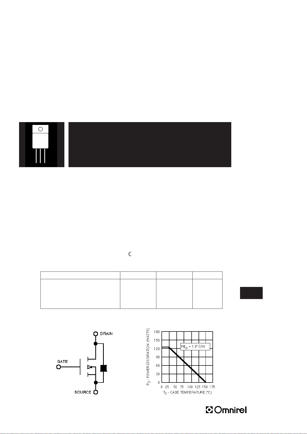
ABSOLUTE MAXIMUM RATINGS (TC= 25°C unless otherwise noted)
Parameter COM150A COM250A COM350A COM450A Units
V
DS
Drain-Source Voltage 100 200 400 500 V
V
DGR
Drain-Gate Voltage (RGS= 1 M ) 100 200 400 500 V
ID@ TC= 25°C Continuous Drain Current
2
±25 ±25 ±13 ±1 1 A
ID@ TC= 100°C Continuous Drain Current
2
±16 ±16 ±8 ±7 A
I
DM
Pulsed Drain Current
1
±100 ±80 ±54 ±40 A
V
GS
Gate-Source Voltage ± 20 ± 20 ±20 ± 20 V
PD@ TC= 25°C Maximum Power Dissipation 125 125 125 125 W
PD@ TC= 100°C Maximum Power Dissipation 50 50 50 50 W
Junction To Case Linear Derating Factor 1. 0 1.0 1. 0 1. 0 W/°C
Junction To Ambient Linear Derating Factor .020 .020 .020 .020 W/°C
T
J
Operating and
T
stg
Storage Temperature Range -55 to 150 -55 to 150 -55 to 150 -55 to 150 °C
Lead Temperature (1/16" from case for 10 secs.) 300 300 300 300 °C
1 Pulse Test: Pulse width 300 µsec. Duty Cycle 2%.
2 Package Pin Limitation = 15 Amps
THERMAL RESISTANCE
R
thJC
Junction-to-Case 1. 0 °C/W
R
thJA
Junction-to-Ambient 50 °C/W Free Air Operation
.144 DIA.
.050
.040
.260
.249
.685
.665
.800
.790
.545
.535
.550
.510
.045
.035
.550
.530
.150 TYP.
.150 TYP.
.005
MECHANICAL OUTLINE
12 3
Pin 1: Drain
Pin 2: Source
Pin 3: Gate
 Loading...