

Page 1

Programmes After Market Services (PAMS)
Technical Documentation
NHB–3
TROUBLESHOOTING
INSTRUCTIONS
Page 2
PAMS
Technical Documentation
AMENDMENT RECORD SHEET
NHB–3
Troubleshooting
Amendment
Number
Date Inserted By Comments
Original 26/97
Page 2
Page 3

PAMS
Technical Documentation
NHB–3 TROUBLESHOOTING INSTRUCTIONS
Contents
Introduction 6
General 6
Baseband Troubleshooting 7
PWR Button Fault 8
Display Selftest Failed 9
No Registration to the System (no serv) 10
Audio Fault 11
Flash Programming ; part 2 13
Flash Programming ; part 3 14
Flash Programming ; part 4 15
Some BB measurements for reference 16
Power circuitry 17
Repairing Instructions for Flash Faulty Units 18
RF Tuning Fails 19
Calib Temperature Sensor 19
AFC Fails 19
RSSI Fails 19
TXI/TXQ Tuning 20
Power Measuring 20
Power Tuning 20
Calib BATT_VOLTAGE = 6.0 V 20
Calib CHARGE_VOLTAGE = 6.0 V 20
Repairing instructions for RF unit 21
Common features 21
Duplex filter 21
NHB–3 Receiver Functional Description 22
Front–end amplifier V501 22
RX–Filter Z505 22
First Mixer V511 22
First Local Buffer V512 22
IF–amplifier V521 22
IF–filter 23
Second Mixer V531 23
Second Local Buffer V532 23
If–amplifier V541 23
IF–filter Z541 23
AGC–amplifier 23
NHB–3
Troubleshooting
Original 26/97
Page 3
Page 4

PAMS
Technical Documentation
Third Mixer 23
Third IF–filter Z551 23
Third If amplifier 24
RX Signal levels and frequencies 24
Setting of PCLocals 24
Signal Levels at Front End 24
Signal Levels at IF (1) 24
Signal Levels at IF (2) 25
Signal Levels at IF (3) 25
TX Unit 26
Modulator circuit,TX–part of CRFRT ( N551 ) 26
Upconversion mixer ( V702 ) 26
TX interstage filters ( Z713 and Z727 ) 26
1st TX–buffer ( V710 ) 26
2nd TX–buffer ( V725 ) 27
3rd TX–buffer ( V736 ) 27
Power amplifier 27
Power control circuitry 27
TX signal levels and frequencies 28
Settings of PCLocals 28
Signal levels of UHF VCO buffer ( V701 ) 28
Signal levels of 1st amplifier 28
Signal levels of 2nd amplifier 28
Signal levels of 3rd amplifier 29
Signal levels of power amplifier 29
Synthesizer 30
Brief describtion of the synthesizer 30
Reference oscillator 30
UHF–part of PLL 30
VHF–part of PLL 30
Synthesizer Signal levels and frequencies 31
UHF Synthesizer Malfunction 31
Setting of PCLocals 31
Synthesizer locked ( Control voltage depends on channel) 31
Voltages of synthesizer N820 : 31
UHF VCO (G1) output: 31
Reference oscillator VCTCXO 32
VHF Synthesizer Malfunction 32
Voltage from Do IF 32
Voltages of N820 32
Biasing voltages on VHF 32
NHB–3
Troubleshooting
Original 26/97
Page 4
Page 5

PAMS
Technical Documentation
Frequency 33
NHB–3
Troubleshooting
Original 26/97
Page 5
Page 6

PAMS
Technical Documentation
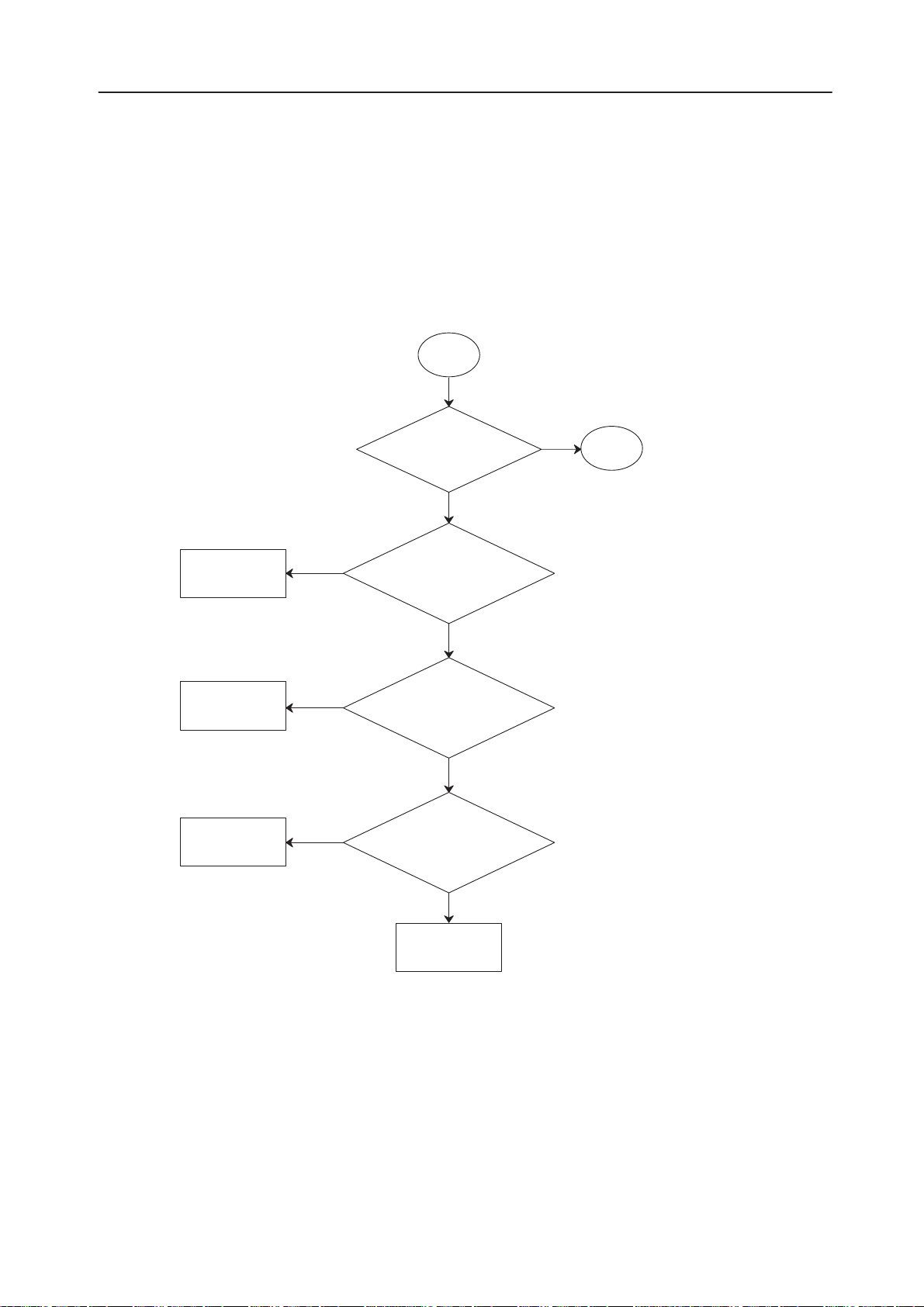
Introduction
General
The purpose is to define fault block of the module and then find out the broken component. The trouble shooting diagram has been planned so that the fault, whatever
it is, can be found by as simple measurements as possible.
The flow diagrams give you the overview of the blocks. The purpose is that you
proceed through the flow diagram so that, if your answer is YES for the asked
question, go straight to the next level, but if your answer is NO, you have to go
the subbranch.
Required servicing equipment:
– PC for PC locals
– Power supply (2.0 A)
– Digital multimeter
NHB–3
Troubleshooting
– Oscilloscope
– Spectrum analyzer
– RF cables
– Modular cable
– RS232/MBUS adapter
– CMT/Marconi
– RF measuring chassis
Original 26/97
Page 6
Page 7

PAMS
Technical Documentation
Baseband Troubleshooting
The following hints should facilitate finding the cause of the problem when the
circuitry seems to be faulty. This troubleshooting guide is divided into the following sections.
1. Power button fault
2. Display self test failed
3. No registration to the system
4. Audio fault
5. Flash programming; part 2
6. Flash programming; part 3
7. Flash programming; part 4
The first thing to do is to carry out a thorough visual check of the module. En-
sure in particular that:
NHB–3
Troubleshooting
a) there is not any mechnical damage
b) soldered joints are OK
Original 26/97
Page 7
Page 8
PAMS
Technical Documentation
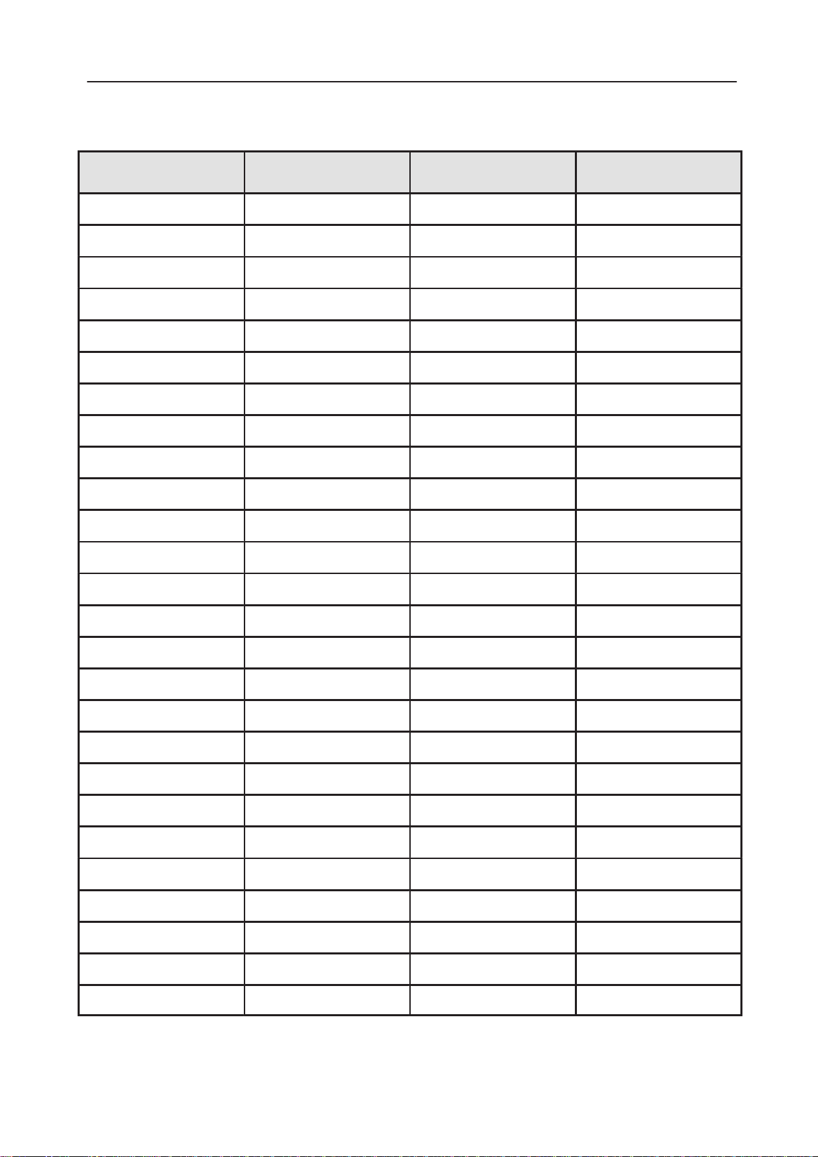
PWR Button Fault
NHB–3
Troubleshooting
Phone does’nt start when
PWR button is pressed
Check
X100
NO
Change
FLEX
Check
X196
N271/PSL
pin 10 +5 V when
VBATT is connected
YES
N271/PSL
pin 10 +5–>0 V when
push PWR button
YES
R110, C113
OK?
Check components
around N271 if OK
change N271
NO
N271/PSL pins 5,2
VBATT voltage
YES
Change
N271
Original 26/97
Page 8
Page 9
PAMS
Technical Documentation
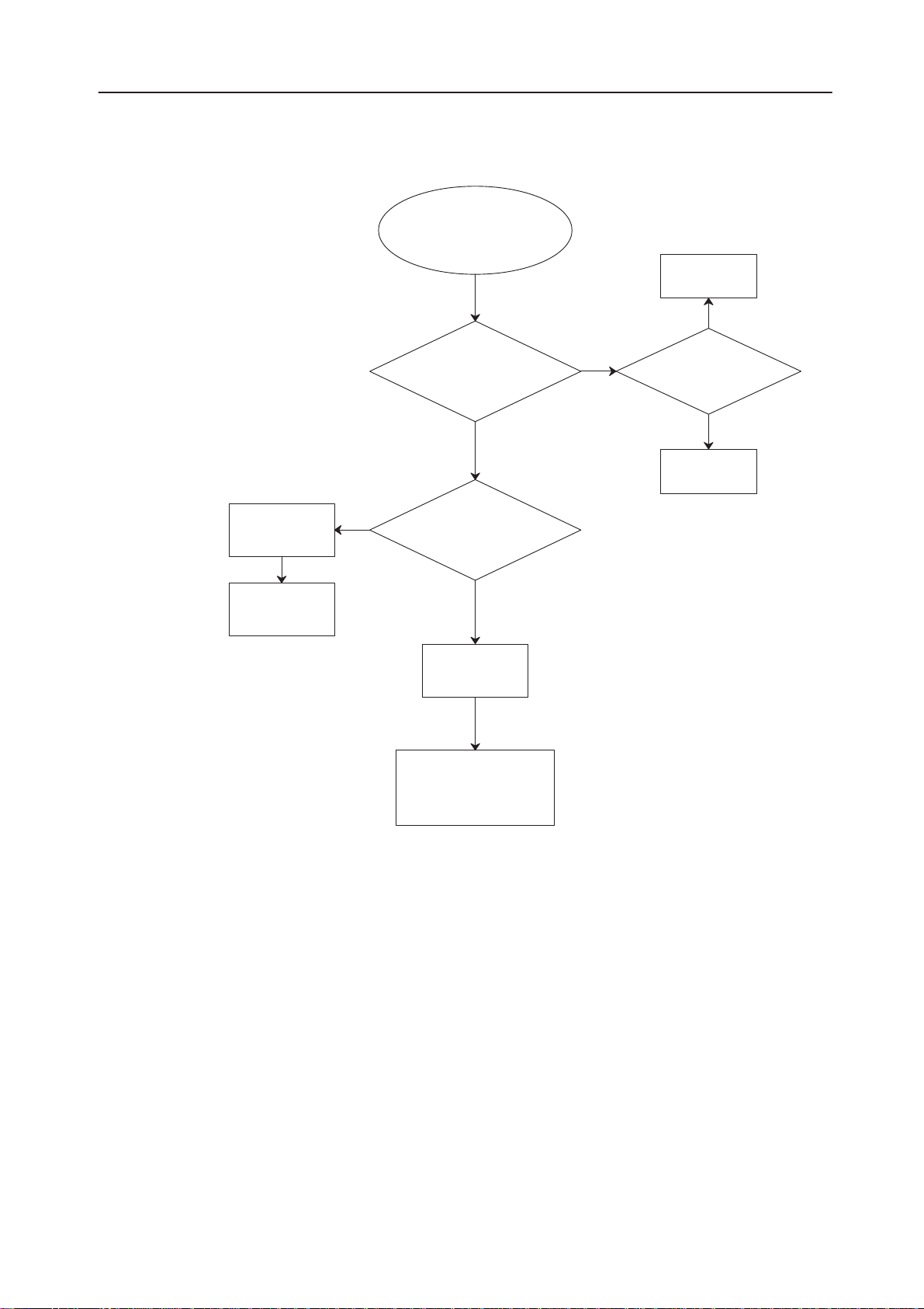
Display Selftest Failed
NHB–3
Troubleshooting
Display selftest failed or
phone doesn’t registrate to
the system (tester)
Use PCLocals to
find out a reason
MCU internal test
MCU RAM bus test
MCU ROM bus test
MCU IMEI test
NO
MCU DSP code
download: failed,
DSP tests: no responce
RFI bus fault
NO
MCU audio codec
test: failed
YES
Codec N260/pin 12 : PCMDO
Codec N260/pin 13 : PCMDI
Codec N260/pin 19 : PCMCLK
Codec N260/pin 20 : XSELPCMC
YES
YES
Unprogrammed FLASH
Unconnected pins in MCU
address or data lines
DSP clock oscillator
DSP pin 45/INT1
DSP pin 10/ERAMHI
DSP pin 9/IOX
DSP pin 12/EROM
DSP pin 14/RWN
DSP pin 15/RWN
DSP pin 39/RSTB
RFI/RFIAD 3:0
RFI/RFIDA 11:0
RFI pin 49/RDX
RFI pin 50/WRX
RFI pin 53/RFICLK
RFI pin 59/RFI2CLK
DSP RAM D210, D211
DSP/DSPDA
DSP/DSPAD
Original 26/97
Page 9
Page 10

PAMS
Technical Documentation
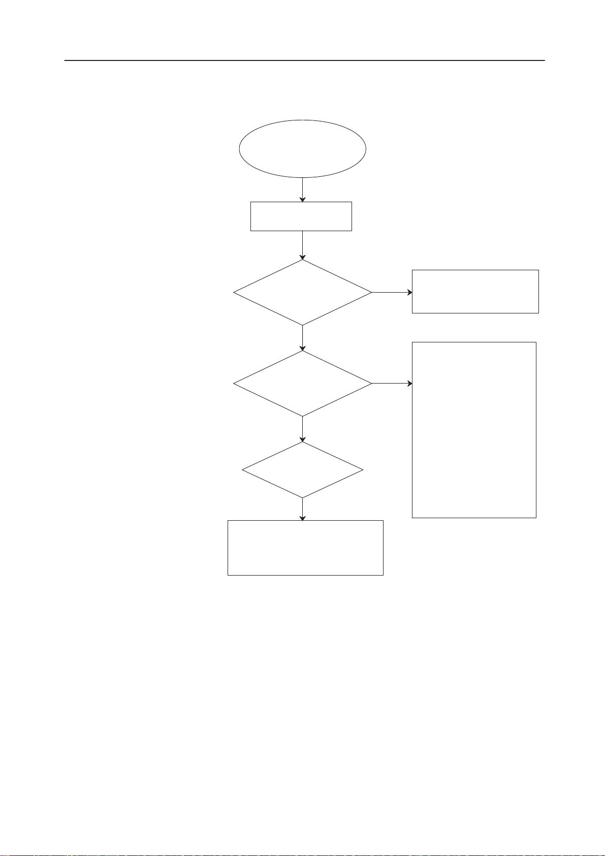
No Registration to the System (no serv)
No registration to the
system (no serv)
no call
Selftest OK
YES
DSP pin 43, 45 INT0, 1 (from ASIC)
RFI pins 1,63/RXI, RXQ
RFI pin 3/EXTBG (4.096 V)
RFI pin 4/VCM (2.35 V)
RFI pin 6/TXC (to RF)
RFI pins 8,9/TXQ+, TXQ– (to RF)
RFI pins 11,12/TXI+, TXI– (to RF)
RFI pin 14/AFC (to RF)
RFI pins 20...23,28,29/PDA TA 5:0
RFI pin 51/DAX (to ASIC)
ASIC/D230/pin 105/SYNTHPWR (to RF)
ASIC/D230/pin 104/TXP (to RF)
ASIC/D230/pin 106/TXPPWR (to RF)
ASIC/D230/pin 111/SENAT (to RF)
ASIC/D230/pin 112/SENAR (to RF)
ASIC/D230/pin 113/SDAT (to RF)
ASIC/D230/pin 114/SCLK (to RF)
NHB–3
Troubleshooting
Original 26/97
Page 10
Page 11
PAMS
Technical Documentation
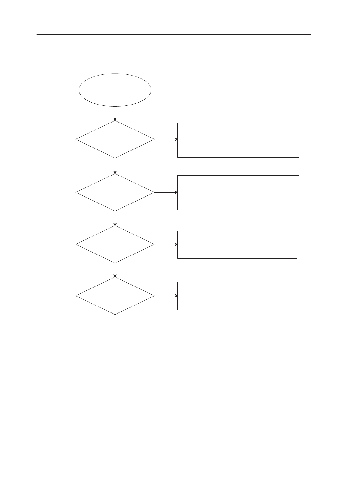
Audio Fault
Audio fault
Microphone or earphone
signal missing
Microphone and
earphone signal
Microphone signal
missing?
NO
missing?
YES
YES
NHB–3
Troubleshooting
CODEC pin 15/SYNC (from ASIC)
CODEC pin 16/CODEC_CLK (from ASIC)
DSP pins 79, 82/PCMCOSYCLKX (from ASIC)
DSP pins 60, 81/PCMDATRCLKX (from ASIC)
DSP pin 80/CODEC_CLK
CODEC N260/pins 22, 23 MICP, MICN
X196/pins 18, 19 MICP, MICN
CODEC N260/pin 10 PCMOUT
CODEC N260/pin 17 MICENA
X196/pin 12 MICENA
NO
Earphone signal
missing?
NO
Missing ringing tones
YES
YES
CODEC N260/pins 6, 7
X196/pins 20, 21
CODEC N260/pin 14/PCMIN
DSP D200/pin 78
MCU/D231/PIN79. NOTE! PWM SIGNAL
X196/PIN22
BUZZER JOINTINGS
CHANGE FLEX
Original 26/97
Page 11
Page 12

PAMS
Technical Documentation
FLASH programming
NHB–3
Troubleshooting
Check X100
C113 OK?
YES
R110 OK?
YES
MBUS
registration
OK?
Power
stays on?
NO
NO
NO
N271/pin 8/XRESET
VBATT
pins 5, 20?
YES
+5 V after pwr on?
NO
YES
YES
Display:
selftest failed
YES
3
Display:
selftest failed
YES
MBUS line X100/5
+5 V after pwr on?
YES
NO
NO
D231/MCU/pin 3; _RD
D230/ASIC/pin 97; RSTROBE
Short circuits in
data lines. Data line
disconnected, VREF
unconnected
NO
R166
+ 5 V?
YES
V160 base
∼1 V
YES
Check R163,
V160, R161,
R160, C160
NO
NO
If D231 at
pin 66/TXD
doesn’t apply
+5 V change
D231
Check
R165, R166
V161, R164
Change N271
Original 26/97
Power supp. to the logic
circuits +5 V after pwr on?
NO
Change N271
MCU/D231/PIN67/RXD
PIN46/TMR1
ASIC/D230/PIN67/MBUSDET
+5 V after pwr on ?
NO
If R162 is OK
change D231
YES
2
YES
Change first
D231
Page 12
Page 13

PAMS
Technical Documentation
Flash Programming ; part 2
NHB–3
Troubleshooting
2
Change D230
YES
26 MHz clock
D230/pin 119?
NO
26 MHz/1 Vpp in
testpoint J113
YES
Check components
D191, D192, R231
R246, R247, C234
NO
MCU/D231/pin 10
RESETX +5 V after
power on?
/pin 8/MD2, MCU/D230
MCU/D231/pin 43
/XPWROFF pulses up to
+5 V after pwr on?
YES
26 MHz at MCU
/D230 pin 69
/MCUCLK?
YES
MCU/D230
/pin 9/_STBY
YES
YES
NO
Change D230
NO
NO
Change D231
Check joints
and foils
Original 26/97
MCU/D231/pin 77
/IRQ0 +5 V after
power on?
YES
MCU/D231/pin 4
/WSTROBEX +5 V
after pwr on?
YES
Check all soldered joints
The data and address signals must
clear a difference between low (0 V)
and high (+5 V)
NO
NO
Change D230
Check D230
Page 13
Page 14
PAMS
Technical Documentation
Flash Programming ; part 3
NHB–3
Troubleshooting
3
Check D230
Check D231
(D230)
Check D231
(D230)
EEPROM
initialization OK?
NO
NO
NO
NO
D184/EEPROM
/pin 27/EROMSELX pulses
+5 to 0 V during r/w
action?
YES
D184/EEPROM
/pin 1/RSTROBEX pulses
+5 to 0 V during r/w
action?
YES
D184/EEPROM
/pin 1/WSTROBEX pulses
+5 to 0 V during r/w
action?
YES
4
Original 26/97
YES
Change D184
Page 14
Page 15

PAMS
Technical Documentation
Flash Programming ; part 4
NHB–3
Troubleshooting
4
D185/FLASH
/pin 11 +12 V during
programming?
YES
D231/MCU
/pin 64/HOOK/RXD2
pulses during prog?
YES
X100/pin 7
/PHFS/TXD2 pulses
during programming?
YES
D185/FLASH
/pin 12/PWD +5 V
after power on?
YES
NO
NO
NO
NO
Check X100/pin 14
C182, R175, R169,
L180
Check X100/pin 6
R177, R178, C176
Check D231/pin63
R184, R185, C186
Check D230
Check D185/FLASH/
ADDRESS/DATA LINES
/no shortcircuits or
unconnected pins allowed
OK
Change D185
Original 26/97
D185/FLASH
/pin 9/ROMSELX pulses
from +5 to 0 V after
power on?
YES
/pin 37/RSTROBEX pulses
YES
/pin 38/WSTROBEX pulses
D185/FLASH
from +5 to 0 V after
power on?
D185/FLASH
from +5 to 0 V after
power on?
NO
NO
NO
Check D231 (D230)
Check D231 (D230)
Check D231 (D230)
Page 15
Page 16

PAMS
Technical Documentation
Troubleshooting
Some BB measurements for reference
Test point Frequency / DAC Level Note
1 N271 : 5, 20 VBatt
2 N271 : 2 / 24 / 1 4.6 V VA1 / VA2 / Vref
3 L272 4.6 V VL 1
3 L273 4.6 V VL 2
9 R279 4.6 V DSPCLKEN
6 D200 : 37, 38 60.2 MHz > 400 mVpp DSPCLK
11 D200 : 40 30 MHz CKO
7 D200 : 39 4.6 V DSPIRSTX
8 D200 : 43, 45 ~ 0V INT0, INT1
5 D231 : 69 26 MHz ~ 5 Vpp MCUCLK
12 D231 : 10 4.6 V RESETX
13 D231 : 77 4.6 V IRQX
NHB–3
10 D231 : 66, 67 4.6 V RXD,TXD (no traffic)
14 D231 pin 52 ~ 3 V VBA TDET
15 D231 pin 53 ~ 1.5 V VC
16 D231 pin 54 DAC : ~ 1020 4.6 V HOOK
17 D231 pin 55 DAC : ~ 460 ~ 2.1 V TBAT
18 D231 pin 56 DAC : ~ 480 ~ 2.1 V TRF
19 D231 pin 57 DAC : ~ 250 ~1.1 V BTYPE
Original 26/97
Page 16
Page 17

PAMS
Technical Documentation
Power circuitry
NHB–3
Troubleshooting
VCTCXO
CLK 26 MHz
VBAT 5.5...8 V
CHRGDET 1.5 V
DETIN
ON
PSL
– Output voltages must be stay at high state at least 1.5 s when power is
– If no; check C113.
5,20
11
12
14
XPWROFF
C113
24
9
switched on.
D192
VL1 MCU CLK
VL2
VREF
1
VA
2
VA2
XRESET
846
ASIC MCUPSL
XPWROFF 2 pulses / sec
BUFFER
CLK 26 MHz
116
RESET
45
IRQX
99
5 V=ON
69
10
77
5,42 66
43
TXD
R166
– If it is OK; replace PSL.
– If the XRESET line doesn’t rise check CHRDET and DETIN. The voltage
ASIC
– When XRESET and CLK are supplied to the ASIC but MCUCLK or RESETX
MCU
– If MCUCLK and RESETX are supplied from ASIC but TXD line (MBUS)
– If TXD pin (MCU) goes to high but doesn’t stay at high state at least 1.5 s.
Original 26/97
value at these pins should be 1.5 V.
to the MCU are not supplied; replace ASIC.
doesn’t rise and solderings of the MCU are good; replace MCU.
The power of the phone can be hold on following way:
– Connect PSL pin 14 to the ground.
– Lift MCU pin 77 IRQ0 and connect it to VL1.
Now its possible to use PCLocals software.
Page 17
Page 18

PAMS
Technical Documentation
Troubleshooting
Repairing Instructions for Flash Faulty Units
1. When the phone doesn’t start (power off after 2 seconds) check following things:
– VBATT is connected to the PSL N271
– XRES rise to high state
– VL1 is 4.7 V
– VREF is connected to the VCTCXO and the crystal is running frequency is
26 MHz
Measure:
– supply voltage of MCU D231
– reset signal for MCU (RESETX) rise high state
– MCU clocksignal is 26 MHz
– NMI line stay low
– IRQ0 rise high state
NHB–3
If things (mentioned above) are ok, the MCU starts supply poweroff pulses to
the PSL N271 and the power stay on.
Most likely IRQ0 stay low, which means that interrupt is generated all the time.
In these cases check data and addresslines of MCU’s and memory circuits.
There are shortcircuits or unconnected pins.
The power can be forced stay on by connected PSL N271 pin 14 to the ground.
2. When FLASH PROGRAMMING is not succeed, check following things:
– System connector X100 pins 6, 7, 14 are soldered and there are no shortcir-
cuits.
– Flash programming voltage (12 V) is connected to D185 pin 11.
– The data and addresslines of flashcircuit D185 are soldered.
– EEPROM D184 should be OK because of the initialization (program param-
eters are loaded always when program is loading the first time).
3. When FACTORY SET is not succeed or the power is switched off after programming:
When power is switched on the program of the phone will start so called maxi-
mum mode and if this doesn’t work there has been a fault during the flash programming.
Original 26/97
Page 18
Page 19

PAMS
Technical Documentation
4. If selftest (A) is failed, check:
– Solderings of EEPROM D184
– Do factory set once again (setup error in EEPROM D184)
5. If selftest (B) is failed, check:
– Measure by oscilloscope that crystal XT1 is running (60.2 MHz).
– Reset signal DSP1RSTX for DSP (D200 pin 39) is high state.
NHB–3
Troubleshooting
– Small clock signal at pins 37, 38 of DSP is greater than 400 mV
– Clock signal at pin 40 (DSP) is 30 MHz (square wave; amplitude 5 V).
– Check solderings of D200, D210 and D211.
6. If the phone takes too small current measure at pins of synthesizer that it’s
working normally.
7. If the phone takes too high current check the outputs of RF regulator that supply
voltages are OK.
PP.
RF Tuning Fails
Calib Temperature Sensor
a) Check R809 and R173
b) Check D231 pin 56
AFC Fails
a) Check AFC control voltage; G1 pin 5
b) Check that RX inj. freq. changes when AFC value is changed in PCLOCALS;
G1 pin 1.
c) Check that correct inj. freq. can be accessed with reasonable AFC values
(–1024...1024); G1 pin 1.
c) Check RX branch gain (see RX signal levels)
d) If a, b and c is OK then check solders of N270 –> change N270
RSSI Fails
a) Check RX branch gain
b) check solders of N270, D200 and D230
Original 26/97
Page 19
Page 20

PAMS
Technical Documentation
TXI/TXQ Tuning
Carrier leagage must be tuned with shields and edge clip on and screws tighten.
Upper side bands amplitude is not allowed to tune to its minimum with amplitude and phase tuning. Because if the data type is changed to another then the
USP signal will be higher => TUNE TO BALANCE.
If there is no signal at N551 pins 21...24, check N270 solders.
IF there is not signal at N551 pin 28 => check input level at pins 16 and 19 and
control pulse at pin 31 .
Power Measuring
If there is not enough power at outputs, check power control loop, power amp.
and duplex filter.
Power Tuning
NHB–3
Troubleshooting
Tune TXC values at TX levels 0, 5, 10, 11 and 15.
Calib BATT_VOLTAGE = 6.0 V
a) Check R112, R113
b) Check N271 pin 23
c) Check D231 pin 52
Calib CHARGE_VOLTAGE = 6.0 V
a) Check R140, R142
b) Check D231 pin 53
Original 26/97
Page 20
Page 21

PAMS
Technical Documentation
Repairing instructions for RF unit
Common features
NHB–3 receiver’s frequency band is 60 MHz. It starts at 1930,2 MHz and ends
at 1989,8 MHz. This band consists 299 channels from 512 to 810. Receiver dynamic range is 96 dB that is composed of 39 dB gainstep in front–end and 57
dB gainstep in AGC–amplifier in CRFRT–circuit.
The frequency band of NHB–3 transmitter is 60 MHz between 1850.2 and
1909.8 MHz. Channel numbering and the amount of channels is similar to RX
side.
TX signal is made by mixing UHF VCO signal and modulated TX intermediate
signal in passive mixer. After mixing TX signal is amplified and filtered by two
amplifiers and dielectric filters. The discrete power amplifier amplifies the TX–
signal to desired power level. Maximum output level after duplex filter is 1.0 W
(30dBm).
NHB–3
Troubleshooting
Duplex filter
HD851 uses helical duplexer which have 3.0 dB maximum insertion loss in receiving band. Minimum attenuation between TX and RX lines is 20 dB.
Original 26/97
Page 21
Page 22

PAMS
Technical Documentation
NHB–3 Receiver Functional Description
Measurements should be done using spectrum analyzer with high–frequency
probe (LO–/reference frequencies and RF –levels) and oscilloscope (DC–voltages and the amplitude of the reference oscillator).
Front–end amplifier V501
The front–end amplifier operates with 5,5 mA current. Base and collector voltages are Vb=0,86V and Vc=3,44V. Front–end gain is controlled by signal PDATA0 which comes from RFI–circuit. PDATA0 controls the switching transistor
V502. Because of low value limit of Vce of V501 the switch is placed in to the
collector of it.
The gain in the front–end amplifier is about 13dB and the attenuation in off–
state is about 26 dB. This means 39 dB gainstep when front–end is turned off.
The signal level when front–end is switched off is –45dBm. Gain is reduced by
feedback resistor R502 for stabilation of the amplifier and to improve the intermodulation in IF–parts.
NHB–3
Troubleshooting
RX–Filter Z505
3 pole ceramic filter is used as RX–filter. Filter has center frequency (f0) of
1960 Mhz and bandwidth of 60 Mhz. Insertion loss in passband is 2.2 dB maximum. Attenuation at the frequency of f0 +100 Mhz is 15 dB minimum and
f0 +400 Mhz is 48 dB minimum.
First Mixer V511
Incoming frequency span is 60 MHz as in the front–end. Conversion loss is
about 6dB maximum. Local signal is driven into the mixer at the level of 3 dBm.
Local signal frequencies are in band of 1617,2 MHz to 1876,8 MHz.
First Local Buffer V512
Buffer operates with 4,7mA current. Base and collector voltages are Vb=0,77V
and Vc=2,33V. This buffer has gain from 10dB t0 11,5dB depending the used
channel (lowest channel has the lowest gain).
IF–amplifier V521
Amplifier operates with 5,7mA current and about 10dB gain. Gain is reduced by
the feedback resistor R521 for stabilation and to improve intermodulation in later IF–parts. Also there is negative feedback done by C528 that is for the first
local signal and it’s harmonics. Base voltage of the transistor is Vb=0,85V and
collector voltage Vc=2,1V.
Original 26/97
Page 22
Page 23

PAMS
Technical Documentation
IF–filter
First IF–filter is made to reject the mirror frequencies of second IF (487MHz).
Second Mixer V531
Second mixer converts 313 MHz first IF to 87 MHz second IF. Conversion loss
is about 6 dB. Local signal is driven in to mixer at level of 3 dBm and the frequency is 400 MHz.
Second Local Buffer V532
Buffer is running at 6,5mA current and base and collector voltages are Vb=0,7V
and Vc=2,2V. Buffer has about 10 dB gain.
If–amplifier V541
amplifier is running with 15mA current and about 14 dB gain. Base–emitter voltage of the transistor is Vb=0,95V and collector–emitter coltage Vce=2,98V.
NHB–3
Troubleshooting
IF–filter Z541
Second IF–filter is narrowband SAW–filter. It takes part of the neighbor channel
filtering. Filter has about 10dB loss in passband.
AGC–amplifier
First part in the CRFRT–circuit is the AGC–amplifer that takes care of 57 dB
gainsteps (20*3dB, 47 dB gain and 10dB attenuation). These gainsteps are
controlled by analog voltage coming from TXC–line. Gainsteps are calibrated in
RSSI–calibration (Front–end gain ON during the calibration).
Third Mixer
Third mixer located in CRFRT is active mixer that converts 87MHz second IF to
13MHz third IF. 400MHz second local signal is fed to CRFRT and divided by 4
for the 100MHz third local signal.
Third IF–filter Z551
Third IF–filter is ceramic filter that does a part of neighbor channel filtering. Filter has about 6 dB loss in passband.
Original 26/97
Page 23
Page 24

PAMS
Technical Documentation
Third If amplifier
Third IF–amplifier is located in CRFRT and it’s a constant gain amplifier with
30dB gain. Signal is brought out with two pins that have different phase shifters
after the CRFRT–circuit. With these phase shifter 90 degree’s phase difference
is accomplished. After the phase shifters signals are fed into the IQ–demodulator that is in RFI–circuit which is located in baseband area.
RX Signal levels and frequencies
Setting of PCLocals
Active unit : RX
Operation mode : Continuous
Continuous Mode : Channel 661
AGC : 81 dB
AGC–DAC : 771
Frontend : ON
NHB–3
Troubleshooting
Signal (–50 dBm, f=1960.06771 MHz) will be connected to the antenna
connector.
Signal Levels at Front End
Test point Position Frequency *Level Note:
Bias 1 V501 B DC 0.87V
Bias 2 V501 C DC 2.54V
1 Z505OUT 1960 MHz –41.5 dBm
Signal Levels at IF (1)
Test point Position Frequency *Level Note:
Bias 3 V512 B DC 0.76V
Bias 4 V512 C DC 2.3V
2 C517/R510 1647 MHz –8.4 dBm
3 V512 C 1647 MHz –1.0 dBm
Bias 5 V521 B DC 0.73V
Bias 6 V521 C DC 2.15V
4 V521B 313 MHz –43.8 dBm
5 V521C 313 MHz –35.2 dBm
Original 26/97
Page 24
Page 25

PAMS
Technical Documentation
Signal Levels at IF (2)
Test point Position Frequency *Level Note:
Bias 7 V532 B DC 0.71V
Bias 8 V532 C DC 2.19V
6 V532 B 400 MHz –11.3 dBm
7 V532 C 400 MHz +9.5 dBm
Bias 9 V541 B DC 1.81V
Bias 10 V541 C DC 4.24V
8 V541 B 87 MHz –46.6 dBm
9 V541 C 87 MHz –26.0 dBm
Signal Levels at IF (3)
Test point Position Frequency *Level Note:
10 RXI 12.932 MHz –3.7 dBm
11 RXQ 12.932 MHz –3.6 dBm
NHB–3
Troubleshooting
Original 26/97
Page 25
Page 26

PAMS
Technical Documentation
TX Unit
Measurements should be done using spectrum analyzer with high–frequency
probe (LO–/reference frequencies and RF –levels) and oscilloscope (DC–voltages and the amplitude of the reference oscillator).
Modulator circuit,TX–part of CRFRT ( N551 )
The modulator is a quadrature modulator contained in TX–section of CRFRT
IC. I– and Q–inputs generated by RFI interface are DC–coupled and fed via
buffers to the modulator. Local signal is divided by two in order to get accurate
90 degrees phase shifted signals to the I/Q mixers. After mixing signals are
combined and amplified with temperature compensation controlled gain amplifier ( TCGA ). The gain of the 1st TX amplifier is about 3dB. The gain is controlled with power control signal TXC. Output of the TCGA is amplified and
max. output level is –10 dBm.
Upconversion mixer ( V702 )
NHB–3
Troubleshooting
Upconversion mixer is a single balanced passive diode mixer. The local signal
is balanced by printed circuit transformer. The mixer upconverts the modulated
IF–signal that comes from quadrature modulator to RF–signal.
Conversion loss is 6–8 dB. Local signal is driven into the mixer at level of 3.0
dBm max. TX–frequency range is 1850–1910 MHz and local freq. range
1650–1710 MHz.
TX interstage filters ( Z713 and Z727 )
Filters are 3–pole ceramic filters. Center frequency f0 is 1880 MHZ and bandwidth is 60 MHz. Insertion loss in passband is 2.2 dB maximum. Attenuations of
the filter are: 15 dB minimum at f0+/–100 MHz, 47 dB min. at f0–400 MHz and
45 dB min. at f0+ 400 MHz.
The filters reject spurious signals generated in the upconversion mixer. They
also reject leakage of local–, image– and IF–signals.
1st TX–buffer ( V710 )
First TX–buffer is a bipolar transistor amplifier which amplifies the TX–signal
coming from the upconversion mixer.
Collector current Ic is 5 mA,Vb=0.7V,Vc=1.9V and gain is about 6dB. Supply
voltage is 4.5V.
Original 26/97
Page 26
Page 27

PAMS
Technical Documentation
2nd TX–buffer ( V725 )
Bipolar transistor amplifier which amplifies the TX–signal coming from 1st interstage filter. Ic=15mA,Vb=0.85V,Vc=3.0V and gain is about 14dB.
Supply voltage is 4.5V.
3rd TX–buffer ( V736 )
3rd buffer is bipolar transistor amplifier. It amplifies the TX–signal coming from
2nd interstage filter. Ic= 40 mA,Vb=0.84V, Vc=3.0V and gain is about 13 dB.
Supply voltage is 4.5V.
Power amplifier
Power amplifier is a two stage discrete amplifier ( V756 and V 765 ). Power amplifier is specified for 6 volts operation. Gain is about 20dB.
Note! When low power levels (i.e levels 11–15) are used, power amplifier is
NOT switched off.
NHB–3
Troubleshooting
Power control circuitry
Power control circuitry consists of power detector and a differential control circuit. Power detector is a combination of a directional coupler and a diode rectifier. The differential control circuit compares the detected voltage and TXC and
controls voltage controlled amplifier ( in CRFRT ) and the power amplifier.
Original 26/97
Page 27
Page 28

PAMS
Technical Documentation
TX signal levels and frequencies
Levels are measured with HP high frequency probe 50Ω 10:1. Supply voltage
6.0V was connected via dummy battery ( type BTS–4 ). PClocals was used to
control the phone. The probe was connected to spectrum analyzer.
Settings of PCLocals
Active unit :TX ( level 0 was used in measurements )
Operation mode :Burst
Continuous mode :OFF
Channel :661 ( mid channel )
Signal levels of UHF VCO buffer ( V701 )
Test point Position Frequency *Level Note:
NHB–3
Troubleshooting
Bias 1 V701 base 0.75V Bias
Bias 2 V701 collector 2.4V Bias
1 V701 base 1680 MHz –15 dBm Local signal
2 V701 collector 1680 MHz 3 dBm Local signal
Signal levels of 1st amplifier
Test point Position Frequency *Level Note:
Bias 3 V710 base 0.70V Bias
Bias 4 V710 collector 1.9V Bias
3 Z713 input 1880 MHz –12 dBm TX–signal
Signal levels of 2nd amplifier
Test point Position Frequency *Level Note:
Bias 5 V725 base 0.85V Bias
Bias 6 V725 collector 3.0V Bias
4 Z713 out 1880 MHz –14 dBm TX–signal
5 Z727 input 1880 MHz 0 dBm TX–signal
Original 26/97
Page 28
Page 29

PAMS
Technical Documentation
Signal levels of 3rd amplifier
Test point Position Frequency *Level Note:
Bias 7 V736 base 0.84V Bias
Bias 8 V736 collector 3.0V Bias
6 Z727 out 1880 MHz –2 dBm TX–signal
7 V736 collector 1880 MHz 11 dBm TX–signal
Signal levels of power amplifier
Test point Position Frequency *Level Note:
bias 9 V756/V765 gate –3.8V Bias
bias 10 V756/V765 drain Vbatt Bias
8 V756 drain 1880 MHz 24 dBm TX–signal
9 Z500 TX 1880 MHz 31 dBm TX–signal
NHB–3
Troubleshooting
Original 26/97
Page 29
Page 30

PAMS
Technical Documentation
Synthesizer
Measurements should be done using spectrum analyzer with high–frequency
probe (LO–/reference frequencies and RF –levels) and oscilloscope (DC–voltages and the amplitude of the reference oscillator).
Brief describtion of the synthesizer
Reference oscillator
The reference oscillator is a discrete VCTCXO consisting of a 26 MHz crystal,
BJT(V801) –oscillator circuit and buffer(V802). The tuning of the oscillator frequency is done via RFI–controlled AFC –line by changing the voltage over the
capacitance diode V800. The appropriate changes in tuning voltages are based
on the calculations performed by software (DSP). The output voltage of the 26
MHz oscillator signal is about 0.7Vpp.
NHB–3
Troubleshooting
NHB–3 uses National’s LMX2331 Dual PLL –circuit (N820) for synthesizing both UHF and VHF LO –frequencies.
UHF–part of PLL
For UHF, the incoming oscillator frequency (26MHz) is first divided by 130 to
form the 200 kHz reference frequency for phase comparison. Loop filter then
low–pass filters the signal down to DC –level, which is used as a control voltage for VCO.
UHF –VCO
UHF –VCO (G1) is a discrete module, which is used to generate the first injection for RX (1617.2 ... 1676.8 MHz) and the final injection for TX (1650.2 ...
1709.8 MHz). The output frequency of the module depends on the DC –control
voltage.
VHF–part of PLL
The reference frequency for VHF PLL is 1 MHz. After phase comparison, the
output signal is low–pass filtered to DC –level, which is used as reverse voltage
for capacitance diode (V842). VHF –VCO is made out of discrete components,
and it consists of BJT(V840) –oscillator circuit and buffer(V841). The output frequency, which is used as second injection for RX, is 400 MHz for all channels.
Original 26/97
Page 30
Page 31

PAMS
Technical Documentation
Synthesizer Signal levels and frequencies
UHF Synthesizer Malfunction
Setting of PCLocals
Active unit : RX or TX
Operation mode : Continuous (RX) or Burst (TX)
Continuous Mode Ch: Channel will be changing
Synthesizer locked ( Control voltage depends on channel)
Test point Position Frequency *Level Note:
1 C821 ~1.5V CMch:512
1 C821 ~2.0V CMch:661
1 C821 ~2.6V CMch:810
NHB–3
Troubleshooting
Voltages of synthesizer N820 :
Test point Position Frequency *Level Note:
2 N820 pins 1,20 DC 4.0V Pow. supply
3 N820 pins 2,19 DC 4.6V Charge pump
UHF VCO (G1) output:
Test point Position Frequency *Level Note:
4 RFOUT DC 4.6V Vcc
5 ” 1617.2 MHz RX / CMch:512
5 ” 1647.0 MHz RX / CMch:661
5 ” 1676.8 MHz RX / CMch:810
5 ” 1650.2 MHz TX / CMch:512
5 ” 1680.0 MHz TX / CMch:661
5 ” 1709.8 MHz TX / CMch:810
Original 26/97
Page 31
Page 32

PAMS
Technical Documentation
Reference oscillator VCTCXO
Test point Position Frequency *Level Note:
6 V800 DC ~2.5V
7 N820 pin 8 26MHz 1V
Bias V801 C DC 3.2V Bias
Bias V801 B DC 1.8V Bias
Bias V801 E DC 1.1V Bias
– check the crystal and other components in oscillator circuit.
VHF Synthesizer Malfunction
Voltage from Do IF
Test point Position Frequency *Level Note:
pp
NHB–3
Troubleshooting
f
ref
8 C823 DC 2.5V (all channels)
Voltages of N820
Test point Position Frequency *Level Note:
9 N820 pins 1,20 DC 4.0V Pow. supply
10 N820 pins 2,19 DC 4.6V Charge pump
Biasing voltages on VHF
Test point Position Frequency *Level Note:
Bias V841 C DC 4.3V Bias
Bias V841 B DC 3.2V Bias
Bias V841 E DC 2.5V Bias
Bias V840 C DC 2.4V Bias
Bias V840 B DC 1.5V Bias
Bias V840 E DC 0.8V Bias
– Check the components surrounding V840 and V841, and make sure that
V842 has been soldered as the component location picture shows it.
– Check the following components: R827, R828, R840, C823, C824, C830,
Original 26/97
C840
Page 32
Page 33

PAMS
Technical Documentation
Frequency
Test point Position Frequency *Level Note:
C850 (VHFLO) 400 MHz (all channels).
UHF– and VHF SYNTHESIZERS OK
To ensure the 400 MHz –signal for the third mixing in N551(CRFRT), check the
following components:
L551, C551, C552, C553
NHB–3
Troubleshooting
Original 26/97
Page 33
Page 34

PAMS
Technical Documentation
NHB–3
Troubleshooting
This page intentionally left blank.
Original 26/97
Page 34
 Loading...