

Page 1

Programmes After Market Services (PAMS)
Technical Documentation
HANDSFREE DESKTOP
CHARGER – CHH–8P
Page 2

PAMS
Technical Documentation
AMENDMENT RECORD SHEET
NHB–3
HF Desktop Charger CHH–8P
Amendment
Number
Date Inserted By Comments
Original 26/97 Page 2
Page 3

PAMS
Technical Documentation
Handsfree Desktop Charger CHH–8P
Contents
HF Desktop Charger CHH–8P Page 4
General Page 4
User Interface Features Page 5
Charging Indication Page 5
Charge States and Charge Control Page 5
Instructions for Use Page 6
Charging the Phone Battery Page 6
Charging the Extra Battery Page 6
Deep Discharging of the Extra Battery Page 7
Handsfree Function Page 7
Using the Voice Mail Page 7
The Data Connection Page 7
Technical Specifications Page 8
Modes of Operation Page 8
External/Internal Signals and Connections Page 8
Functional Description Page 13
Supply Voltages Page 13
Control Logic Page 13
Port A Signals of the Processor Page 14
Port B Signals of the Processor Page 14
Port C Signals of the Processor Page 14
Port D Signals of the Processor Page 15
Port F Signals of the Processor Page 15
Processor A/D Inputs Page 15
Watchdog Circuits Page 16
Battery Charging Page 16
Spare Battery Discharging Page 16
Microphone Amplifier and Corresponding Switches Page 17
Speaker Amplifier and Corresponding Swithes Page 17
Block Diagram of CHH–8 Page 18
Circuit Diagram of DC3 Power Supply and Control Module Page 19
Circuit Diagram of DC3 Audio Switches and Amplifiers Page 20
Circuit Diagram of Connector Module DC4 Page 21
Layout and Foil Diagrams of DC4 Page 23
Parts List of DC3 Code: 0200211 Page 24
Parts List of DC4 Code: 0200235 Page 31
Exploded View Page 32
Assembly Parts Page 33
NHB–3
HF Desktop Charger CHH–8P
Original 26/97 Page 3
Page 4
PAMS
Technical Documentation
HF Desktop Charger CHH–8P
Related Documentation
6E 0200211 parts list of DC3
6E 0200235 parts list of DC4
S 0675026 exploded view
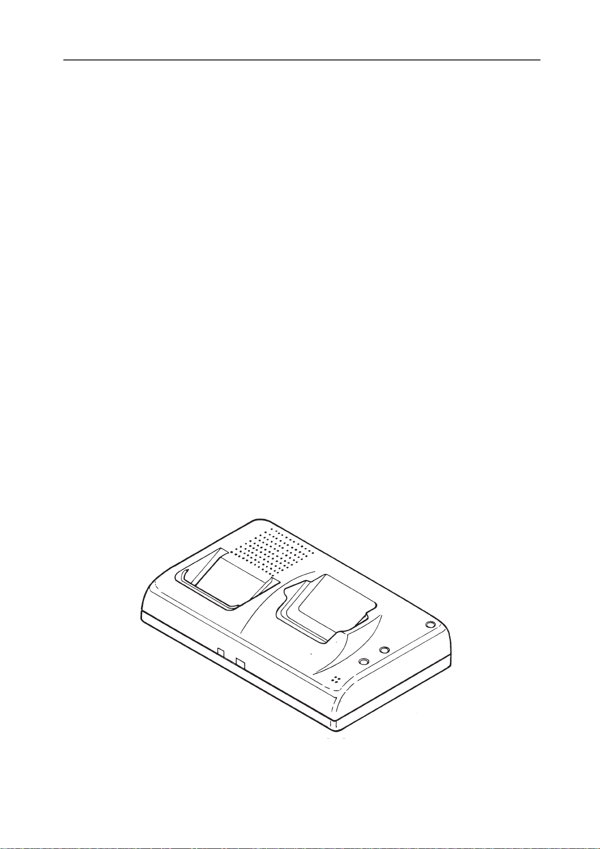
General
The HF desktop charger CHH–8P is for the second generation digital
handportable telephones. HF desktop charger is designed for charging
the handportable phone and the spare battery. It provides handsfree function
when the phone is on the charger and there is also a connector for data
accessories. CHH–8P is designed for to be used in the office environment with
the power supply ACS–6.
NHB–3
HF Desktop Charger CHH–8P
circuit diagram of DC3
circuit diagram of DC4
9853931 layout & foil diagr. DC3
9853930 layout & foil diagr. DC4
0260218 mechanics
CHH–8P consists of spare battery charging control processor, charging
indicators and switching mode power supply for charging the phone and the
spare battery. The unit has inbuilt HF speaker and HF microphone but the actual handsfree function is generated in the phone. There are also three operating
buttons. The front one is for muting the microphone during a call, the middle
one is for the voice mail listening and the rear one is for the spare battery
discharge.
Original 26/97 Page 4
Page 5

PAMS
Technical Documentation
User Interface Features
HF desktop charger is designed for charging the handportable phone and the
spare battery. It provides also handsfree function when the phone is on the
charger. The unit has inbuilt HF speaker and HF microphone but the actual
handsfree function is generated in the phone. There are also three operating
buttons. The front one is for muting the HF microphone, the middle one is for
the voice mail listening and the rear one is for the spare battery discharging.
Charging takes place at a battery temperatures of 5...45 Centigrade. Charge
control of the phone is done with phone microprocessor and charge control of
extra battery is done with separate microprocessor located in a desktop stand.
Phone is always charged first, then extra battery.
A battery gives better capacity if it is occasionally discharged completely. User
can do this by using the ‘deep discharge‘ –feature of CHH–8P. This feature is
provided only extra battery slot and pressing the ‘discharge‘ –button. The extra
battery will then automatically be discharged and charged to full. If this button is
pressed twice then the discharge function is cancelled.
NHB–3
HF Desktop Charger CHH–8P
Charging Indication
Charge is indicated with two dual–colors led‘s, one for the phone and one for
the extra battery pack. The liquid–crystal display of the phone also contains a
three–bar battery display.
Leds are dimmed when there is no phone or extra battery connected.
Right led for handportable:
Red phone led indicates a fast charge mode of the phone battery.
Green phone led indicates that the phone battery is full and tricle charge mode
is on.
Left led for spare battery:
Red spare battery led indicates that the battery is not full; either there is a fast
charge mode active or charging is disabled due to a battery temperature or to
fast charge mode of the phone.
Green spare battery led indicates that the battery is full.
Flashing red spare battery led indicates that a discharge cycle is activated.
Charge States and Charge Control
Charge current for the phone is supplied through a series switch transistor in
the phone. When this transistor is on the charger is supplying a constant
current to the phone. This is the rapid charge mode.
When the transistor is off no current is supplied to the phone and the charger is
in the constant voltage mode.
Original 26/97 Page 5
Page 6

PAMS
Technical Documentation
Having been charged up in the rapid charge mode, the battery is kept in full
charge using pulsed charging, i.e. switching power alternately on and off at a
variable duty cycle and a frequency of a few Hz.
The desktop charger is also provided with control logic for spare battery charging, which is allowed when no phone is connected or when the phone is in the
pulsed charge mode.
Instructions for Use
Plug in the ACS–6 AC power supply to the mains outlet. Connect the cord from
ACS–6 to the dc connector at the rear of the CHH–8 HF desktop charger.
Charging the Phone Battery
Place the phone into the recess in the charger. The right–hand indicator at the
front edge of the charger shows the charge of the phone battery. The red led is
lit during quick charging, and once the phone battery has reached full charge,
the green led alights, showing that only trickle charging is on.
NHB–3
HF Desktop Charger CHH–8P
When the phone is powered, the charge can be read from three indicator bars
appearing on the phone display. During the quick charging phase, each bar is lit
alternately for one second. Once the battery is fully charged all three bars are
lit. If the charger indicator is not lit when the phone is on the charger, ensure
that the phone is properly in place and that the power supply is correctly
plugged to the charger and to the wall outlet.
The battery will not accept charge if its temperature is below +5 C or above
+45 C.
Charging the Extra Battery
Place the extra battery into the recess in the charger. The left hand indicator of
the charger shows battery charge. During quick charging, the red indicator is lit
and once the battery has reached full charge, the green indicator alights showing trickle charging. If the phone and the extra battery are on the charger at the
same time the phone battery is charged first, followed by charging of the extra
battery.
If the charger indicator is off when the extra battery is installed on the charger,
ensure that the extra battery is properly in place and that the power supply is
correctly plugged in to the charger and to the wall outlet.
The battery will not accept charge at a temperature of below +5 C or above
+45 C.
Original 26/97 Page 6
Page 7

PAMS
Technical Documentation
Deep Discharging of the Extra Battery
In the interests of best possible battery efficiency, it is recommended that the
battery be deep discharged once a week or so.
To start the deep discharge function, press once the discharge key at the rear
of the charger, whereupon the red indicator showing extra battery charging
starts to flash. Once the battery has been discharged, the charger will automatically start charging it. Should you wish to interrupt discharging, press the discharge key again. The indicator ceases to flash and the charger will resume
battery charging. It is not recommendable to deep discharge a fully charged
battery.
Handsfree Function
When installed in the charging stand, the phone is always in the handsfree
mode of operation. The internal HF speaker and HF microphone are then
activated for the call. It is also possible to turn the phone into HF mode and off
while a call is going on. This is done by removing the phone or placing it on the
charger.
NHB–3
HF Desktop Charger CHH–8P
HF speaker volume is adjusted at the phone volume key, and an outgoing call
can be muted by presssing at the mute key on the front edge of the charger.
The muted state is indicated by the message ”MUTED” on the phone display.
Pressing the key once more cancels muting, shown by the text ”UNMUTED”
which appears on the display for a moment.
Using the Voice Mail
The voice–mail key in the middle of the charger is for calling one’s voice mailbox in the network switching centre and listening to voice messages. When
calling the voice mailbox, the first press on the key makes the call to the
mailbox and the second ends the call.
The Data Connection
The charger contains a 10–pin modular connector for data accessories
(e.g. PCMCIA card).
Original 26/97 Page 7
Page 8

PAMS
Technical Documentation
Technical Specifications
Modes of Operation
Power off mode: If the unit doesn’t receive power supply to the d.c.
connector there isn’t any voltage on the module.
Standby mode: The unit receives supply voltage to the d.c. connector.
The processor is running but because there isn’t any
phone or spare battery on the cradle, the charger is off
and the audio functions are inactive.
Active mode: The telephone or spare battery is on the cradle so the
charging functions are active. Normally the handsfree
speaker is muted. During a call and during the key
beeps or alarming tones the speaker and corresponding
audio switches are open.
External/Internal Signals and Connections
NHB–3
HF Desktop Charger CHH–8P
The charger has four external and three internal connectors, the AC fast charger connector, the spare battery connector, phone system connector, the data
accessory connector, internal system connector, internal speaker connector
and internal microphone connector.
AC Fast Charger Connector X100
Pin: Line: Function:
1 VDC Supply voltage
2 DGND Power supply ground
Spare Battery Connector X101
Pin: Line: Function:
1, 2, 3 GND Supply power ground
4 BTEMP Battery temperature sensing
5 BSI Battery size identification
6, 7, 8 VBAT Charging voltage
Original 26/97 Page 8
Page 9

PAMS
Technical Documentation
Phone System Connector X701
Pin: Line: Function:
1 DGND Power supply ground
2 XMIC Microphone signal
3 AGND Analog ground
4 TDA Transmitted data
5 M2BUS Serial bidirection bus
6 HOOK Not used
7 PHFS Not used
8 VC Supply/charging
9 DGND Power supply ground
10 XEAR/HFJWR Earphone signal/CHH–8 power switch
11 DSYNC Data syncronisation
NHB–3
HF Desktop Charger CHH–8P
12 RDA Received data
13 BIND Not used
14 VF Not used
15 DCLK Data clock
16 VC Supply/charging
Data Accessory Connector X510
Pin: Line: Function:
1 DSYNC Datasyncronisation
2 +VD Supply voltage
3 DGND Supply power good
4 M2BUS Serial bidirection data
5 RDA Received data
6 TDA Transmitted data
7 AGND Analog ground
8 XMIC Microphone signal
9 XEAR Earphone signal
10 DCLK Data clock
Original 26/97 Page 9
Page 10

PAMS
Technical Documentation
Internal System Connector X500/DC3, X700/DC4
Pin: Line: Function:
1, 2 VC Supply/charging
3 +5V
4 PHFS Not used
5 DGND Power supply ground
6 DSYNC Data syncronisation
7 DCLK
8 TDA Transmitted data
9 RDA Received data
10 DGND Power supply ground
11 M2BUS Serial bidirection bus
12, 14 AGND Analog ground
NHB–3
HF Desktop Charger CHH–8P
13 XEAR Earphone signal
14 AGND Analog groud
15 XMIC Microphone signal
16 AGND Analog ground
17, 18 DGND Power supply ground
Internal Speaker Connector X460/DC3
Pin: Line: Function:
1 HFSPK HF speaker signal
2 AGND Analog ground
External Microphone Connector X440/DC3
Pin: Line: Function:
1 HFMIC HF microphone signal
2 AGND Analog ground
Original 26/97 Page 10
Page 11

PAMS
Technical Documentation
Supply Voltages and Power Consumption on the Connectors of CHH–8
Symbol: Description: Values:
VDC Supply voltage
• input voltage min/typ/max:
• input power max:
VBAT Spare battery voltage
• charging volt. min/typ/max:
• charging curr. min/typ/max:
• discharg. volt. min/typ/max:
• discharg. curr. min/typ/max:
VC Charging voltage
• output voltage min/typ/max:
• output current min/typ/max:
VD Data signal
• output voltage min/typ/max:
• output current max:
HF Desktop Charger CHH–8P
11.0...13.8...20.0 V
13 W
11.0...12.2...13.0 V
730...800...870 mA
5.0...6.0...7.5 V
130...160...200 mA
11.0....12.2...13.0 V
730...800...870 mA
9.5...10.0...10.5 V
50 mA
NHB–3
Supply Voltages and Power Consumption on the DC3 Module
Symbol: Description: Values:
+VL Supply voltage for LED’s
• voltage min/typ/max:
• current max:
+VCC Cahrging voltage for the battery
• voltage min/typ/max:
• current min/typ/max:
+VE Supply for empty battery
• voltage min/typ/max:
• current max:
+5V Supply for 5 V logic parts
• voltage min/typ/max:
• current max:
+VA Supply for analog power switch
• voltage min/typ/max:
• current max:
11.0...13.8...20 V
50 mA
10.3...11.5...13.3 V
730...800...870 mA
4.9...5.0...5.1 V
100 mA
4.9...5.0...5.1 V
50 mA
9.6...10.0...10.4 V
200 mA
+VAN Supply for analog parts
• voltage min/typ/max:
• current max:
+VAS Switched supply for speaker amp.
• voltage min/typ/max:
• current max:
Original 26/97 Page 11
4.9...5.0...5.1 V
20 mA
9.3...9.7...10.1 V
200 mA
Page 12

PAMS
Technical Documentation
HF Desktop Charger CHH–8P
+VREF Ref. voltage for analog parts
• voltage min/typ/max:
• current max:
2.4...2.4...3.1 V
5 mA
Supply Voltages and Power Consumption on the DC4 Module
Symbol: Description: Values:
+5V Supply for 5 V logic parts
• voltage min/typ/max:
• current max:
4.75...5.0...5.25 V
15 mA
AC Characteristic (1 kHz)
Symbol: Description: Values:
XMIC External microphone signal
• Cable level:
• 0 dBmO:
200 mV
415 mV
NHB–3
RMS
RMS
HFMIC Handsfree microhone signal
• MRP, mic ref point.:
• HFMIC, about 20 dB atten.:
• Gain for HFMIC:
• Cable level:
XEAR External earphone signal
• Cable level:
• 0 dBmO:
HFSP Handsfree speaker signal
• Cable level:
• Gain for HFSP:
+15.3 dBPa 50 cm
–4.7 dBPa
40 dB
200 mV
130 mV
411 mV
130 mV
RMS
RMS
RMS
RMS
17 dB
Original 26/97 Page 12
Page 13

PAMS
Technical Documentation
Functional Description
The DC3 module electronics consists of the following functional blocks:
– Supply voltages
– Control logic
– Battery charging
– Spare battery discharging
– Watchdog circuit
– Microphone amplifier and corresponding switches
– Speaker amplifier and corresponding switches
Supply Voltages
The supply voltage +VI (11.0 V– 20.0 V) for the DC3– and DC4–modules is
taken from the power supply connector X100 connected to the Power Supply
ACS–6.
NHB–3
HF Desktop Charger CHH–8P
The battery charging voltage +VCC (10.0 V – 13.0 V) is connected to the phone
or to the spare battery.
+VE voltage (5.0 V) is generated by the regulator N150 to charge totally empty
battery to the +5.0 V level.
+VA voltage (10.0 V) is the supply for the analog parts. From that voltage are
generated also analog voltages +VAN (5.0 V) and +VAS (10.0 V). Reference
voltage +VREF (2.75 V) for the analog is made by the N430–A from the +VAN
voltage.
+5V voltage is the supply for digital parts, generated by the regulator N103.
Control Logic
The phone battery and spare battery charging indication, spare battery
charging and discharging, audio connections and activation of voice mail are
controlled by processor D300. It is a single–chip type controller incorporating
RAM, ROM, A/D converter and a multifunction timer/counter.
The processor communicates with the handphone via the M2BUS. The M2BUS
interface comprises transistors V200, V201 and corresponding resistors.
Original 26/97 Page 13
Page 14

PAMS
Technical Documentation
Port A Signals of the Processor
Port A: Function:
PA0: PHONE GREEN (out) Phone LED control, green: ”1”
PA1: PHONE RED (out) Phone LED control, red: ”1”
PA2: SPARE GREEN (out) Spare battery LED control, green: ”1”
PA3: SPARE RED (out) Spare battery LED control, red: ”1”
PA4: DISCHRG BUTTON (in) Discharge button control, ”0”: start discharge
PA5: SPARE DISCHRG (out) Discharge spare battery, ”1”: discharge enabled
PA6: AUDIO POWER (out) Audio power switch, ”1”: power on
PA7: CHARGER (out) Charger switch, ”1”: charger on
Port B Signals of the Processor
Port B: Function:
NHB–3
HF Desktop Charger CHH–8P
PB0: SERVICE J301(out)
PB1: SERVICE J302(out)
PB2: SERVICE J303 (out)
PB3: SERVICE J304 (out)
PB4: SERVICE J305 (out) NC
PB5: VOICE MAIL (in) Voice mail listening, ”0”: activation
PB6: HFMIC MUTE (in) HF microphone muting, ”0”: activation
PB7: Unused NC
Port C Signals of the Processor
Port C: Function:
PC0: TXD (out) M2BUS transmit
PC1: RXD (in) M2BUS receive
PC2: Unused NC
PC3: TRXDINT (in) M2BUS interrupt
PC4: DVCE0 (in) Device type, ”1”
PC5: DVCE1 (in) Device type, ”0”
PC6: SPARE CHARGE (out) Spare battery charging, ”1”: charging on
PC7: WTCHDOG (out) Watchdog reset, ”01010...”: reseting on
Original 26/97 Page 14
Page 15

PAMS
Technical Documentation
Port D Signals of the Processor
Port D: Function:
PD0: PHONE MIC (out) Analog switch, ”1”: phone mic switched on
PD1: ACC MIC (out) Analog switch, ”1”: accessory mic switched on
PD2: HF MIC (out) Analog switch, ”1”: HF mic swithed on
PD3: PHONE EAR (out) Analog switch, ”1”: phone ear swithed on
PD4: ACC EAR (out) Analog switch, ”1”: accessory ear swithed on
PD5: HF SPK (out) Analog switch, ”1”: HF speaker swithed on
PD6: Unused NC
PD7: Unused NC
Port F Signals of the Processor
Not used.
NHB–3
HF Desktop Charger CHH–8P
Processor A/D Inputs
Name: Function:
AN0: VBATL Battery voltage
AN1: VBATH High resolution battery voltage
AN2: PHOCURDET Phone current detect
AN3: BATTEMP Battery temperature, 27 kΩ pull–up resistor to
AN4: BATTSZ Battery size, 100 kΩ pull–up resistor to +5 V
AN5: CHRGVOLT Charger voltage detection
AN6: PWR Phone connection detection
• range: 0...11 V
• resolution 43 mV/bit
• range: 7.0...11 V
• resolution 16 mV/bit
• PDET = ”1” for A/D value higher than 5
• PDET = ”0” for A/D value or less
+5 V reference supply
reference supply
AN7: LIREF Lithium battery detection
Original 26/97 Page 15
Page 16

PAMS
Technical Documentation
Watchdog Circuits
Under normal operation the processor is pulsating the WTCHDOG–line to
reseting the ”power off”– and ”software reset”–watchdogs.
If the processor doesn’t run correctly, then the transistor V210 turns off and the
”Software reset”–watchdog V211 gives reset pulse through C211 to the RESET–line. If after this reseting the processor still runs incorrectly, then the ”Power off”–watchdog (V212, V213) turns off the +5 V regulator N103.
Battery Charging
Charging current for the phone battery is fed in via transistor V311, which is
always on when the phone is connected to the system connector X701 on the
DC4 module. Phone battery charging state is indicated by the red (V344, V345)
and green (V333) leds. Because the phone and the spare battery cannot be
charged at the same time the charging current of the phone must be detected
and this is done with the current mirror V321 and corresponding resistors.
Charging current for the spare battery is fed in via switching transistor V221
and schotky diode V220. The transistor is controlled by the processor (SPARE
CHARGE –line). When the phone battery is not charged and it is allowed to
charge the spare battery, the transistor is on and a constant current is supplied
to the battery (the red led V331 lits). In the pulsed charging mode the charging
current is adjusted by pulsating this charge current (the green led V330 lits).
NHB–3
HF Desktop Charger CHH–8P
Spare battery voltage and ∆V–voltage are determined by reading the VBAT line
state. Voltages are measured through resistor divider R250 / R251 and the amplifier N250–B.
Spare battery size is determined by reading the BSI line state. This is pulled to
+5 V reference voltage by R243. In the battery pack a ”size” resistor is connected between BSI and GND.
Temperature is measured over the BTEMP line. This line is pulled to +5 V
reference voltage by R242. In the battery pack an NTC resistor is connected
between BTEMP and GND.
Spare Battery Discharging
The desktop charger is also provided with a discharge function. This is
activated by pressing the discharge button S300. Resistors R230–R237
determines the discharge current which is fed through switching transistor V230
controlled by the processor. The discharging is indicated by blinking of the red
led V331. The battery is discharged to +5 V and thereafter charged normally to
full.
Original 26/97 Page 16
Page 17

PAMS
Technical Documentation
HF Desktop Charger CHH–8P
Microphone Amplifier and Corresponding Switches
Transistor amplifier circuit V420 and corresponding resistors and capasitors
supplies bias current for microphone. Operational amplifier N430–B is used to
amplify the microphone signal to the handphone. The gain of this amplifier is
about 40 dB. The HF microphone signal is fed to the phone through the analog
switches D400–B and D400–C. The microphone signal XMIC from the Data Accessory (X510) is fed to the phone through the switches D400–A and D400–C.
The supply voltage for the amplifier and the analog switched are taken from the
+VAN regulator N102. The +VREF reference voltage (≅ +2.75 V) is made with
the N430–A from the +VAN analog voltage ( ≅ +5.0 V) .
Speaker Amplifier and Corresponding Swithes
XEAR signal from the phone is fed to the HF speaker through the analog
swithes D410–C and D410–B. The signal is amplified about 17 dB with the
resistors R460, R461 and the amplifier N460. The speaker can be muted with
the MUTE–signal controlled by the prosessor.
NHB–3
XEAR signal from the phone can be fed to the Data Accessory (X510) through
the analog switches D410–C and D410–A.
The supply voltage +VAS (≅ +9.7 V) for the speaker amplifier is taken through
the transistor V341, controlled by the processor, from the +VA regulator N100
(≅+10.0 V).
Original 26/97 Page 17
Page 18

PAMS
Technical Documentation
Block Diagram of CHH–8
DC CONNECTOR
CHARGER
NHB–3
HF Desktop Charger CHH–8P
DC3 MODULE
PHONE
CHARGING
INDICATION
DC4 MODULE
DATA
BUFFER
SPARE BATTERY CONNECTOR
SPARE
BATTER Y
CHARGING
DISCHARG.
CONTROL
BUTTONS
NOICE
REDUC.
PROCESSOR
COMP.
SYSTEM CONNECTOR
/
AUDIO
DATA CONNECTOR
CHARGING LEDS
SPEAKER HFMIC
Original 26/97 Page 18
Page 19

PAMS
Technical Documentation
HF Desktop Charger CHH–8P
Circuit Diagram of DC3 Power Supply and Control Module
NHB–3
Original 26/97 Page 19
Page 20

PAMS
Technical Documentation
HF Desktop Charger CHH–8P
Circuit Diagram of DC3 Audio Switches and Amplifiers
NHB–3
Original 26/97 Page 20
Page 21

PAMS
Technical Documentation
Circuit Diagram of Connector Module DC4
NHB–3
HF Desktop Charger CHH–8P
Original 26/97 Page 21
Page 22

PAMS
Technical Documentation
Layout and Foil Diagrams of DC4
NHB–3
HF Desktop Charger CHH–8P
Original 26/97 Page 22
Page 23

PAMS
Technical Documentation
HF Desktop Charger CHH–8P
Parts List of DC3 Code: 0200211
ITEM CODE DESCRIPTION VALUE TYPE
R103 1411123 Melf resistor 0.22 5 % 0.2 W 0204
R116 1414452 Chip resistor 10.0 k 1 % 0.063 W 0805
R117 1413635 Chip resistor 100 k 5 % 0.063 W 0805
R118 1415600 Melf resistor 1.0 k 1 % 0.2 W 0204
R119 1412423 Chip resistor 4.7 k 5 % 0.063 W 0805
R120 1415784 Melf resistor 4.75 k 1 % 0.2 W 0204
R122 1413635 Chip resistor 100 k 5 % 0.063 W 0805
R123 1415600 Melf resistor 1.0 k 1 % 0.2 W 0204
R127 1414420 Chip resistor 680 k 5 % 0.063 W 0805
R130 1411669 Chip resistor 22 5 % 0.063 W 0805
R200 1412430 Chip resistor 10 k 5 % 0.063 W 0805
R201 1413635 Chip resistor 100 k 5 % 0.063 W 0805
R202 1412729 Chip resistor 33 k 5 % 0.063 W 0805
R203 1413635 Chip resistor 100 k 5 % 0.063 W 0805
R204 1412430 Chip resistor 10 k 5 % 0.063 W 0805
R205 1413917 Chip resistor 150 5 % 0.063 W 0805
R206 1413635 Chip resistor 100 k 5 % 0.063 W 0805
R209 1412423 Chip resistor 4.7 k 5 % 0.063 W 0805
R215 1412536 Chip resistor 22 k 5 % 0.063 W 0805
R216 1414533 Chip resistor 56 k 1 % 0.063 W 0805
R218 1412536 Chip resistor 22 k 5 % 0.063 W 0805
R219 1421108 Melf resistor 30.1 k 1 % 0.2 W 0204
R220 1413917 Chip resistor 150 5 % 0.063 W 0805
R221 1413917 Chip resistor 150 5 % 0.063 W 0805
R222 1413603 Chip resistor 47 k 5 % 0.063 W 0805
R223 1412423 Chip resistor 4.7 k 5 % 0.063 W 0805
R230 1415576 Melf resistor 301 1 % 0.2 W 0204
R231 1415576 Melf resistor 301 1 % 0.2 W 0204
R232 1415576 Melf resistor 301 1 % 0.2 W 0204
R233 1415576 Melf resistor 301 1 % 0.2 W 0204
R234 1415576 Melf resistor 301 1 % 0.2 W 0204
R235 1415576 Melf resistor 301 1 % 0.2 W 0204
R236 1415576 Melf resistor 301 1 % 0.2 W 0204
R237 1415576 Melf resistor 301 1 % 0.2 W 0204
R238 1412430 Chip resistor 10 k 5 % 0.063 W 0805
R240 1414533 Chip resistor 56 k 1 % 0.063 W 0805
R241 1414452 Chip resistor 10.0 k 1 % 0.063 W 0805
R242 1415664 Melf resistor 27.4 k 1 % 0.2 W 0204
R243 1414283 Chip resistor 100 k 1 % 0.063 W 0805
R244 1412423 Chip resistor 4.7 k 5 % 0.063 W 0805
R245 1413603 Chip resistor 47 k 5 % 0.063 W 0805
R246 1413603 Chip resistor 47 k 5 % 0.063 W 0805
R247 1416107 Melf resistor 5.62 k 1 % 0.2 W 0204
NHB–3
Original 26/97 Page 23
Page 24

PAMS
Technical Documentation
R248 1416040 Melf resistor 56.2 k 1 % 0.2 W 0204
R249 1413603 Chip resistor 47 k 5 % 0.063 W 0805
R250 1416160 Melf resistor 100 k 1 % 0.2 W 0204
R251 1416202 Melf resistor 121 k 1 % 0.2 W 0204
R252 1416040 Melf resistor 56.2 k 1 % 0.2 W 0204
R253 1416160 Melf resistor 100 k 1 % 0.2 W 0204
R254 1413603 Chip resistor 47 k 5 % 0.063 W 0805
R255 1413603 Chip resistor 47 k 5 % 0.063 W 0805
R256 1414124 Chip resistor 120 k 5 % 0.063 W 0805
R257 1413635 Chip resistor 100 k 5 % 0.063 W 0805
R258 1412430 Chip resistor 10 k 5 % 0.063 W 0805
R300 1413635 Chip resistor 100 k 5 % 0.063 W 0805
R301 1412729 Chip resistor 33 k 5 % 0.063 W 0805
R302 1412423 Chip resistor 4.7 k 5 % 0.063 W 0805
R303 1412423 Chip resistor 4.7 k 5 % 0.063 W 0805
R304 1412423 Chip resistor 4.7 k 5 % 0.063 W 0805
R310 1413635 Chip resistor 100 k 5 % 0.063 W 0805
R311 1413635 Chip resistor 100 k 5 % 0.063 W 0805
R312 1413635 Chip resistor 100 k 5 % 0.063 W 0805
R313 1413635 Chip resistor 100 k 5 % 0.063 W 0805
R314 1412335 Chip resistor 1.0 k 5 % 0.063 W 0805
R315 1413635 Chip resistor 100 k 5 % 0.063 W 0805
R320 1414533 Chip resistor 56 k 1 % 0.063 W 0805
R321 1414283 Chip resistor 100 k 1 % 0.063 W 0805
R322 1413829 Chip resistor 10 5 % 0.063 W 0805
R323 1414283 Chip resistor 100 k 1 % 0.063 W 0805
R324 1414533 Chip resistor 56 k 1 % 0.063 W 0805
R330 1412536 Chip resistor 22 k 5 % 0.063 W 0805
R331 1412536 Chip resistor 22 k 5 % 0.063 W 0805
R335 1412536 Chip resistor 22 k 5 % 0.063 W 0805
R336 1412536 Chip resistor 22 k 5 % 0.063 W 0805
R337 1412254 Chip resistor 270 5 % 0.063 W 0805
R338 1412198 Chip resistor 56 5 % 0.063 W 0805
R339 1412254 Chip resistor 270 5 % 0.063 W 0805
R341 1413635 Chip resistor 100 k 5 % 0.063 W 0805
R400 1413917 Chip resistor 150 5 % 0.063 W 0805
R401 1413635 Chip resistor 100 k 5 % 0.063 W 0805
R402 1413635 Chip resistor 100 k 5 % 0.063 W 0805
R403 1413635 Chip resistor 100 k 5 % 0.063 W 0805
R404 1413635 Chip resistor 100 k 5 % 0.063 W 0805
R405 1413635 Chip resistor 100 k 5 % 0.063 W 0805
R406 1413635 Chip resistor 100 k 5 % 0.063 W 0805
R410 1413635 Chip resistor 100 k 5 % 0.063 W 0805
R411 1413635 Chip resistor 100 k 5 % 0.063 W 0805
R412 1413917 Chip resistor 150 5 % 0.063 W 0805
R413 1413635 Chip resistor 100 k 5 % 0.063 W 0805
R414 1413635 Chip resistor 100 k 5 % 0.063 W 0805
R415 1413635 Chip resistor 100 k 5 % 0.063 W 0805
HF Desktop Charger CHH–8P
NHB–3
Original 26/97 Page 24
Page 25

PAMS
Technical Documentation
R416 1413635 Chip resistor 100 k 5 % 0.063 W 0805
R420 1414043 Chip resistor 1.8 k 5 % 0.063 W 0805
R421 1413635 Chip resistor 100 k 5 % 0.063 W 0805
R430 1412729 Chip resistor 33 k 5 % 0.063 W 0805
R431 1412729 Chip resistor 33 k 5 % 0.063 W 0805
R440 1413917 Chip resistor 150 5 % 0.063 W 0805
R441 1413917 Chip resistor 150 5 % 0.063 W 0805
R442 1413603 Chip resistor 47 k 5 % 0.063 W 0805
R443 1414109 Chip resistor 15 k 5 % 0.063 W 0805
R444 1414109 Chip resistor 15 k 5 % 0.063 W 0805
R445 1412303 Chip resistor 330 5 % 0.063 W 0805
R446 1412729 Chip resistor 33 k 5 % 0.063 W 0805
R447 1413917 Chip resistor 150 5 % 0.063 W 0805
R460 1413610 Chip resistor 68 k 5 % 0.063 W 0805
R461 1414452 Chip resistor 10.0 k 1 % 0.063 W 0805
R462 1412423 Chip resistor 4.7 k 5 % 0.063 W 0805
R463 1413635 Chip resistor 100 k 5 % 0.063 W 0805
R464 1413850 Chip resistor 4.7 5 % 0.063 W 0805
R500 1412430 Chip resistor 10 k 5 % 0.063 W 0805
R501 1412430 Chip resistor 10 k 5 % 0.063 W 0805
R502 1413635 Chip resistor 100 k 5 % 0.063 W 0805
R520 1412423 Chip resistor 4.7 k 5 % 0.063 W 0805
R530 1413836 Chip resistor 47 5 % 0.063 W 0805
R533 1413836 Chip resistor 47 5 % 0.063 W 0805
R534 1412303 Chip resistor 330 5 % 0.063 W 0805
C100 2310343 Ceramic cap. 22 p 5 % 50 V 0805
C101 2310343 Ceramic cap. 22 p 5 % 50 V 0805
C103 2309517 Ceramic cap. 100 n 10 % 50 V 1206
C104 2501605 Electrol. cap. 100 µ 20 % 35 V RM3.5
C109 2501605 Electrol. cap. 100 µ 20 % 35 V RM3.5
C110 2309517 Ceramic cap. 100 n 10 % 50 V 1206
C111 2502736 Electrol. cap. 220 µ 20 % 16 V 3.5MM
C112 2502736 Electrol. cap. 220 µ 20 % 16 V 3.5MM
C114 2310343 Ceramic cap. 22 p 5 % 50 V 0805
C115 2310752 Ceramic cap. 10 n 20 % 50 V 0805
C116 2604431 Tantalum cap. 10 µ 20 % 16 V 6.0x3.2x2.8
C117 2604209 Tantalum cap. 1.0 µ 20 % 16 V 3.2x1.6x1.8
C118 2502736 Electrol. cap. 220 µ 20 % 16 V 3.5MM
C119 2310343 Ceramic cap. 22 p 5 % 50 V 0805
C120 2310343 Ceramic cap. 22 p 5 % 50 V 0805
C121 2310343 Ceramic cap. 22 p 5 % 50 V 0805
C122 2309517 Ceramic cap. 100 n 10 % 50 V 1206
C123 2307816 Ceramic cap. 47 n 20 % 25 V 0805
C124 2307816 Ceramic cap. 47 n 20 % 25 V 0805
C128 2310752 Ceramic cap. 10 n 20 % 50 V 0805
C129 2309884 Ceramic cap. 4.7 p 0.25 % 50 V 0805
C150 2310544 Ceramic cap. 1.0 n 5 % 50 V 0805
C151 2309517 Ceramic cap. 100 n 10 % 50 V 1206
HF Desktop Charger CHH–8P
NHB–3
Original 26/97 Page 25
Page 26

PAMS
Technical Documentation
C152 2604431 Tantalum cap. 10 µ 20 % 16 V 6.0x3.2x2.8
C153 2604431 Tantalum cap. 10 µ 20 % 16 V 6.0x3.2x2.8
C160 2310449 Ceramic cap. 150 p 5 % 50 V 0805
C210 2502736 Electrol. cap. 220 µ 20 % 16 V 3.5MM
C211 2604209 Tantalum cap. 1.0 µ 20 % 16 V 3.2x1.6x1.8
C212 2310343 Ceramic cap. 22 p 5 % 50 V 0805
C213 2310343 Ceramic cap. 22 p 5 % 50 V 0805
C220 2307816 Ceramic cap. 47 n 20 % 25 V 0805
C240 2307816 Ceramic cap. 47 n 20 % 25 V 0805
C241 2307816 Ceramic cap. 47 n 20 % 25 V 0805
C242 2307816 Ceramic cap. 47 n 20 % 25 V 0805
C243 2307816 Ceramic cap. 47 n 20 % 25 V 0805
C244 2309517 Ceramic cap. 100 n 10 % 50 V 1206
C250 2307816 Ceramic cap. 47 n 20 % 25 V 0805
C251 2307816 Ceramic cap. 47 n 20 % 25 V 0805
C252 2310449 Ceramic cap. 150 p 5 % 50 V 0805
C253 2307816 Ceramic cap. 47 n 20 % 25 V 0805
C300 2310343 Ceramic cap. 22 p 5 % 50 V 0805
C301 2310343 Ceramic cap. 22 p 5 % 50 V 0805
C302 2307816 Ceramic cap. 47 n 20 % 25 V 0805
C303 2307816 Ceramic cap. 47 n 20 % 25 V 0805
C310 2310343 Ceramic cap. 22 p 5 % 50 V 0805
C320 2307816 Ceramic cap. 47 n 20 % 25 V 0805
C340 2310544 Ceramic cap. 1.0 n 5 % 50 V 0805
C341 2309517 Ceramic cap. 100 n 10 % 50 V 1206
C342 2307816 Ceramic cap. 47 n 20 % 25 V 0805
C343 2310343 Ceramic cap. 22 p 5 % 50 V 0805
C400 2604209 Tantalum cap. 1.0 µ 20 % 16 V 3.2x1.6x1.8
C401 2310343 Ceramic cap. 22 p 5 % 50 V 0805
C402 2604209 Tantalum cap. 1.0 µ 20 % 16 V 3.2x1.6x1.8
C403 2604209 Tantalum cap. 1.0 µ 20 % 16 V 3.2x1.6x1.8
C404 2604209 Tantalum cap. 1.0 µ 20 % 16 V 3.2x1.6x1.8
C405 2307816 Ceramic cap. 47 n 20 % 25 V 0805
C410 2310343 Ceramic cap. 22 p 5 % 50 V 0805
C411 2604209 Tantalum cap. 1.0 µ 20 % 16 V 3.2x1.6x1.8
C412 2604209 Tantalum cap. 1.0 µ 20 % 16 V 3.2x1.6x1.8
C413 2604209 Tantalum cap. 1.0 µ 20 % 16 V 3.2x1.6x1.8
C414 2604209 Tantalum cap. 1.0 µ 20 % 16 V 3.2x1.6x1.8
C415 2307816 Ceramic cap. 47 n 20 % 25 V 0805
C420 2310343 Ceramic cap. 22 p 5 % 50 V 0805
C421 2310343 Ceramic cap. 22 p 5 % 50 V 0805
C422 2310343 Ceramic cap. 22 p 5 % 50 V 0805
C423 2310343 Ceramic cap. 22 p 5 % 50 V 0805
C424 2604209 Tantalum cap. 1.0 µ 20 % 16 V 3.2x1.6x1.8
C430 2307816 Ceramic cap. 47 n 20 % 25 V 0805
C431 2604209 Tantalum cap. 1.0 µ 20 % 16 V 3.2x1.6x1.8
C432 2310343 Ceramic cap. 22 p 5 % 50 V 0805
C440 2310343 Ceramic cap. 22 p 5 % 50 V 0805
HF Desktop Charger CHH–8P
NHB–3
Original 26/97 Page 26
Page 27

PAMS
Technical Documentation
C441 2310752 Ceramic cap. 10 n 20 % 50 V 0805
C442 2604431 Tantalum cap. 10 µ 20 % 16 V 6.0x3.2x2.8
C443 2310752 Ceramic cap. 10 n 20 % 50 V 0805
C444 2310343 Ceramic cap. 22 p 5 % 50 V 0805
C445 2310544 Ceramic cap. 1.0 n 5 % 50 V 0805
C446 2310343 Ceramic cap. 22 p 5 % 50 V 0805
C447 2310343 Ceramic cap. 22 p 5 % 50 V 0805
C448 2310544 Ceramic cap. 1.0 n 5 % 50 V 0805
C449 2310343 Ceramic cap. 22 p 5 % 50 V 0805
C450 2310343 Ceramic cap. 22 p 5 % 50 V 0805
C451 2604209 Tantalum cap. 1.0 µ 20 % 16 V 3.2x1.6x1.8
C452 2310343 Ceramic cap. 22 p 5 % 50 V 0805
C460 2604209 Tantalum cap. 1.0 µ 20 % 16 V 3.2x1.6x1.8
C461 2310738 Ceramic cap. 4.7 n 20 % 50 V 0805
C463 2604209 Tantalum cap. 1.0 µ 20 % 16 V 3.2x1.6x1.8
C464 2310343 Ceramic cap. 22 p 5 % 50 V 0805
C465 2310343 Ceramic cap. 22 p 5 % 50 V 0805
C466 2310343 Ceramic cap. 22 p 5 % 50 V 0805
C467 2604431 Tantalum cap. 10 µ 20 % 16 V 6.0x3.2x2.8
C468 2604431 Tantalum cap. 10 µ 20 % 16 V 6.0x3.2x2.8
C469 2310343 Ceramic cap. 22 p 5 % 50 V 0805
C470 2502736 Electrol. cap. 220 µ 20 % 16 V 3.5MM
C471 2309517 Ceramic cap. 100 n 10 % 50 V 1206
C472 2310343 Ceramic cap. 22 p 5 % 50 V 0805
C473 2310784 Ceramic cap. 100 n 10 % 25 V 0805
C500 2310343 Ceramic cap. 22 p 5 % 50 V 0805
C501 2310343 Ceramic cap. 22 p 5 % 50 V 0805
C510 2310343 Ceramic cap. 22 p 5 % 50 V 0805
C511 2310343 Ceramic cap. 22 p 5 % 50 V 0805
C512 2310343 Ceramic cap. 22 p 5 % 50 V 0805
C513 2310343 Ceramic cap. 22 p 5 % 50 V 0805
C514 2310343 Ceramic cap. 22 p 5 % 50 V 0805
C515 2310343 Ceramic cap. 22 p 5 % 50 V 0805
C516 2310343 Ceramic cap. 22 p 5 % 50 V 0805
C517 2310343 Ceramic cap. 22 p 5 % 50 V 0805
C520 2310343 Ceramic cap. 22 p 5 % 50 V 0805
C521 2310343 Ceramic cap. 22 p 5 % 50 V 0805
C522 2310343 Ceramic cap. 22 p 5 % 50 V 0805
C523 2310343 Ceramic cap. 22 p 5 % 50 V 0805
C550 2310343 Ceramic cap. 22 p 5 % 50 V 0805
C551 2310343 Ceramic cap. 22 p 5 % 50 V 0805
C552 2310343 Ceramic cap. 22 p 5 % 50 V 0805
C553 2310343 Ceramic cap. 22 p 5 % 50 V 0805
C554 2310343 Ceramic cap. 22 p 5 % 50 V 0805
C555 2310343 Ceramic cap. 22 p 5 % 50 V 0805
C556 2310343 Ceramic cap. 22 p 5 % 50 V 0805
C599 2604209 Tantalum cap. 1.0 µ 20 % 16 V 3.2x1.6x1.8
C600 2309517 Ceramic cap. 100 n 10 % 50 V 1206
HF Desktop Charger CHH–8P
NHB–3
Original 26/97 Page 27
Page 28

PAMS
Technical Documentation
L100 3606946 Ferrite bead 0.2 Ω 26 Ω/100 MHz 1206
L101 3606946 Ferrite bead 0.2 Ω 26 Ω/100 MHz 1206
L104 3606946 Ferrite bead 0.2 Ω 26 Ω/100 MHz 1206
L105 3606946 Ferrite bead 0.2 Ω 26 Ω/100 MHz 1206
L106 3608519 Chip coil 1.2 µ 5 % 1206
L107 3608519 Chip coil 1.2 µ 5 % 1206
L108 3607555 Coil 125 µ 2 A
L109 0164030 Choke 9 µ
L500 3606946 Ferrite bead 0.2 Ω 26 Ω/100 MHz 1206
L501 3608519 Chip coil 1.2 µ 5 % 1206
L502 3606946 Ferrite bead 0.2 Ω 26 Ω/100 MHz 1206
L503 3608519 Chip coil 1.2 µ 5 % 1206
B301 4500822 Crystal 11.0592 M CL30PF H=3.6 mm
V100 4113828 Trans. supr. 28 V 28 A 600 W DO214AA
V102 4215954 MosFet RFD14N05 n–ch 50 V 10 A TO252
V103 4107027 Zener diode BZX84 5 % 16 V 0.3 W SOT23
V104 4210106 Transistor BSR19 npn 14 V 0.6 A SOT23
V106 4200917 Transistor BC848B/BCW32 npn 30 V 100 mA SOT23
V108 4210108 Transistor BSR20 pnp 12 V 0.6 A SOT23
V110 4107160 Zener diode BZX84 5 % 12 V 0.3 W SOT23
V114 4108639 Diode x 2 BAS28 75 V 250 mA SOT143
V115 4108639 Diode x 2 BAS28 75 V 250 mA SOT143
V117 4107027 Zener diode BZX84 5 % 16 V 0.3 W SOT23
V120 4107027 Zener diode BZX84 5 % 16 V 0.3 W SOT23
V121 4108639 Diode x 2 BAS28 75 V 250 mA SOT143
V200 4200917 Transistor BC848B/BCW32 npn 30 V 100 mA SOT23
V201 4200917 Transistor BC848B/BCW32 npn 30 V 100 mA SOT23
V212 4108639 Diode x 2 BAS28 75 V 250 mA SOT143
V213 4110074 Schottky diode STPS340U 40 V 3 A SOD6
V220 4110074 Schottky diode STPS340U 40 V 3 A SOD6
V221 4210020 Transistor BCP69–25 pnp 20 V SOT223
V222 4200917 Transistor BC848B/BCW32 npn 30 V 100 mA SOT23
V230 4200226 Darl. transistor BCV27 npn 30 V 300 mA SOT23
V240 4100567 Sch. diode x 2 BAS70–04 70V15 mA SERSOT23
V250 4100567 Sch. diode x 2 BAS70–04 70V15 mA SERSOT23
V310 4200909 Transistor BC858B/BCW30 pnp 30 V 100 mA SOT23
V311 4210020 Transistor BCP69–25 pnp 20 V SOT223
V312 4200917 Transistor BC848B/BCW32 npn 30 V 100 mA SOT23
V320 4110074 Schottky diode STPS340U 40 V 3 A SOD6
V330 4864378 Led Green 2.2 V 0805
V331 4864380 Led Red 0805
V333 4864378 Led Green 2.2 V 0805
V334 4864380 Led Red 0805
V335 4864380 Led Red 0805
V336 4200917 Transistor BC848B/BCW32 npn 30 V 100 mA SOT23
V337 4200917 Transistor BC848B/BCW32 npn 30 V 100 mA SOT23
V338 4200917 Transistor BC848B/BCW32 npn 30 V 100 mA SOT23
V339 4200917 Transistor BC848B/BCW32 npn 30 V 100 mA SOT23
HF Desktop Charger CHH–8P
NHB–3
Original 26/97 Page 28
Page 29

PAMS
Technical Documentation
V341 4108639 Diode x 2 BAS28Ω 75 V 250 mA SOT143
V420 4200917 Transistor BC848B/BCW32 npn 30 V 100 mA SOT23
V460 4200909 Transistor BC858B/BCW30 pnp 30 V 100 mA SOT23
D300 4340034 IC, RAM MCU16/8 QFP64
D400 4309488 IC, 4 x bi.switch 74HC4066 SO14S
D410 4309488 IC, 4 x bi.switch 74HC4066 SO14S
N100 4309222 IC, regulator L4810 0.4 A SOT82
N101 4305236 IC, 2 x comp. LM2903 SO8S
N102 4375012 IC, PSL p–supp NMP75012 SO20
N103 4301062 IC, regulator LP2951AC SO8S
N250 4309576 IC, 2 x op.amp. TLC27M2I SO8
N430 4309576 IC, 2 x op.amp. TLC27M2I SO8
N460 4309022 IC, AF amp 1 W 4 Ω 15 V TDA7233 SO8
S300 5200914 Push button switch 2–pole 6x7 smd SMD
S301 5200914 Push button switch 2–pole 6x7 smd SMD
S302 5200914 Push button switch 2–pole 6x7 smd SMD
X100 5414943 Dc–jack d6.3/2 pcb
X101 5431702 Flexfoil connect 1x08 1 mm smd
X440 5416640 Connector 2–pole right angle 1.5 1.5
X460 5416640 Connector 2–pole right angle 1.5 1.5
X500 5431704 Flexfoil connect 1x18 0.8 mm smd
X510 5401050 Modular jack 10 shielded pcb
6500001 Crystal insulating plate HC–49/U
9380149 Sticker brady lat–2–747 9.5x9.5
9853931 PC board DC3 94.0x123.9x1.6 m6 2/pa
HF Desktop Charger CHH–8P
NHB–3
Original 26/97 Page 29
Page 30

PAMS
Technical Documentation
HF Desktop Charger CHH–8P
NHB–3
Parts List of DC4 Code: 0200235
ITEM CODE DESCRIPTION VALUE TYPE
R700 1413635 Chip resistor 100 k 5 % 0.063 W 0805
R701 1412335 Chip resistor 1.0 k 5 % 0.063 W 0805
R702 1413635 Chip resistor 100 k 5 % 0.063 W 0805
R703 1412335 Chip resistor 1.0 k 5 % 0.063 W 0805
R704 1413635 Chip resistor 100 k 5 % 0.063 W 0805
R705 1412335 Chip resistor 1.0 k 5 % 0.063 W 0805
R706 1413917 Chip resistor 150 5 % 0.063 W 0805
C700 2310343 Ceramic cap. 22 p 5 % 50 V 0805
C701 2310343 Ceramic cap. 22 p 5 % 50 V 0805
C706 2310752 Ceramic cap. 10 n 20 % 50 V 0805
C707 2310752 Ceramic cap. 10 n 20 % 50 V 0805
C708 2310343 Ceramic cap. 22 p 5 % 50 V 0805
C709 2307816 Ceramic cap. 47 n 20 % 25 V 0805
C710 2310343 Ceramic cap. 22 p 5 % 50 V 0805
C711 2310343 Ceramic cap. 22 p 5 % 50 V 0805
L700 3606946 Ferrite bead 0.2 Ω 26 Ω/100 MHz 1206
L701 3608519 Chip coil 1.2 µ 5 % 1206
L703 0164030 Choke 9 µ
V700 4108639 Diode x 2 BAS28 75 V 250 mA SOT143
V701 4108639 Diode x 2 BAS28 75 V 250 mA SOT143
V702 4108639 Diode x 2 BAS28 75 V 250 mA SOT143
D700 4340858 IC, 8xh/l level shift so1 74HC4050 SO16S
X700 5431704 Flexfoil connect 1x18 0.8 mm smd
X701 5469778 Accessory connector hd720 smd
9853930 PC board DC4 22.0x60.0x1.6 d 15/pa
Original 26/97 Page 30
Page 31

PAMS
Technical Documentation
Exploded View
NHB–3
HF Desktop Charger CHH–8P
Original 26/97 Page 31
Page 32

PAMS
Technical Documentation
HF Desktop Charger CHH–8P
Assembly Parts
ITEM Q’TY CODE DESCRIPTION VALUE, TYPE
1 7 6293042 PT screw KB22x8 FeZn clr
2 4 6501067 Adhesive foot d=8 h=2 clr
3 9450258 Bottom cover 1D 23095
4 5140444 Cond. microphone 63 ±2 dB
5 9460012 Microphone pad 4D 21140
6 7133162 Flex foil 18x0.5 0.8 mm clr
7 5140460 Loudspeaker 8 Ω 2 W d=45 h=19
8 9460054 Speaker seal ring 3D 22231
9 5409552 Battery connector with flex
10 9460088 Light guide 3D 22994
11 9450257 Front cover 1D 23094
12 3 9460087 Discharge button 4D 22992
13 9480052 Speaker screen 4D 22694
14 9380154 Type label 4D 22419
15 9560009 Ballast 4D 23334
C1 0200211 DC3 module
C2 0200235 DC4 module
NHB–3
Original 26/97 Page 32
Page 33

PAMS
Technical Documentation
NHB–3
HF Desktop Charger CHH–8P
This page intentionally left blank.
Original 26/97 Page 33
 Loading...