

Page 1

Programmes After Market Services (PAMS)
Technical Documentation
NHB–3 Series Transceiver
NHB–3 Series Transceiver
Chapter 5
UIF MODULE GU8
Page 2

PAMS
Technical Documentation
CHAPTER 5 – UIF MODULE DU8
CONTENTS
Page No
Introduction 5–3
Technical Outline 5–3
Mechanics 5–3
Electronics 5–4
List of Submodules and Mechanical Parts 5–5
Technical Specifications 5–5
Maximum Ratings 5–5
DC Characteristics 5–5
Control Signals 5–6
AC Characteristics 5–6
External Signals and Connections 5–7
Mechanical Characteristics 5–9
Functional Description 5–9
Circuit Description 5–9
DU8C Circuit Description 5–9
Keyboard scanning and display driver control 5–9
Keyboard and display illumination 5–9
Audio Circuitry 5–10
LCD Module Interface 5–10
SIM interface 5–11
Power Distribution Diagram 5–11
Assembly 5–12
Construction 5–12
Assembly Description 5–12
Flexi Diagram 5–14
Assembly Parts of UIF Module DU8 5–14
Testing 5–14
Recommended Test Equipment 5–14
Test Procedure 5–14
Circuit Diagram of DU8 5–15
Layout and Foil Diagram 5–16
NHB–3
UIF Module DU8
Original 26/97
Page 5–2
Page 3

PAMS
Technical Documentation
Introduction
NOTE! UIM (User Identity Module) = SIM (Subscriber Identity Module)
DU8C UI–module ismade for HD851 project. It is used also in HD851EFR product. UI–module is based on GSM/PCN UI–module DU8. Two capacitors pads
added for 18pF capacitors (2320041) from microphone pins to ground. Reason
why capacitors are added is noise to microphone audio in certain situations.
Also some changes are done for reability and productivity reasons. DU8C UI–
module is for NOKIA1 design. Final product use only one 18pF capacitor between microphone pins.
Technical Outline
Mechanics
The module is made from a single flexible printed circuit board – loaded with all
the parts for the User Interface Module. A flexible circuit was used for a number of reasons:
NHB–3
UIF Module DU8
– The material is only 0.3 mm thick – so the phone’s height buildup can be
kept to a minimum.
– The Volume keys, SIM interface and microphone wiring can be folded to fit
in the phone during assembly – since the circuit is flexible.
– Connection from the UIF to the main circuit board can be made with a fold-
ing termination.
The major mechanical parts on the UIF assembly include the following:
– Display Module:– LCD, Heat seal, LCD driver TAB circuit and Light guide.
– Main Keydome assembly: Adhesive film holding 20 metal dome clickers
– Volume & Power Keydome assemblies: Adhesive film (2 films for Style 1)
holding 3 (2 + 1 for Style 1) domes for Vol Up, Vol Down & Power Key.
– Acoustic Components: microphone, speaker, buzzer.
Original 26/97
Page 5–3
Page 4
PAMS
Technical Documentation
NHB–3
UIF Module DU8
Electronics
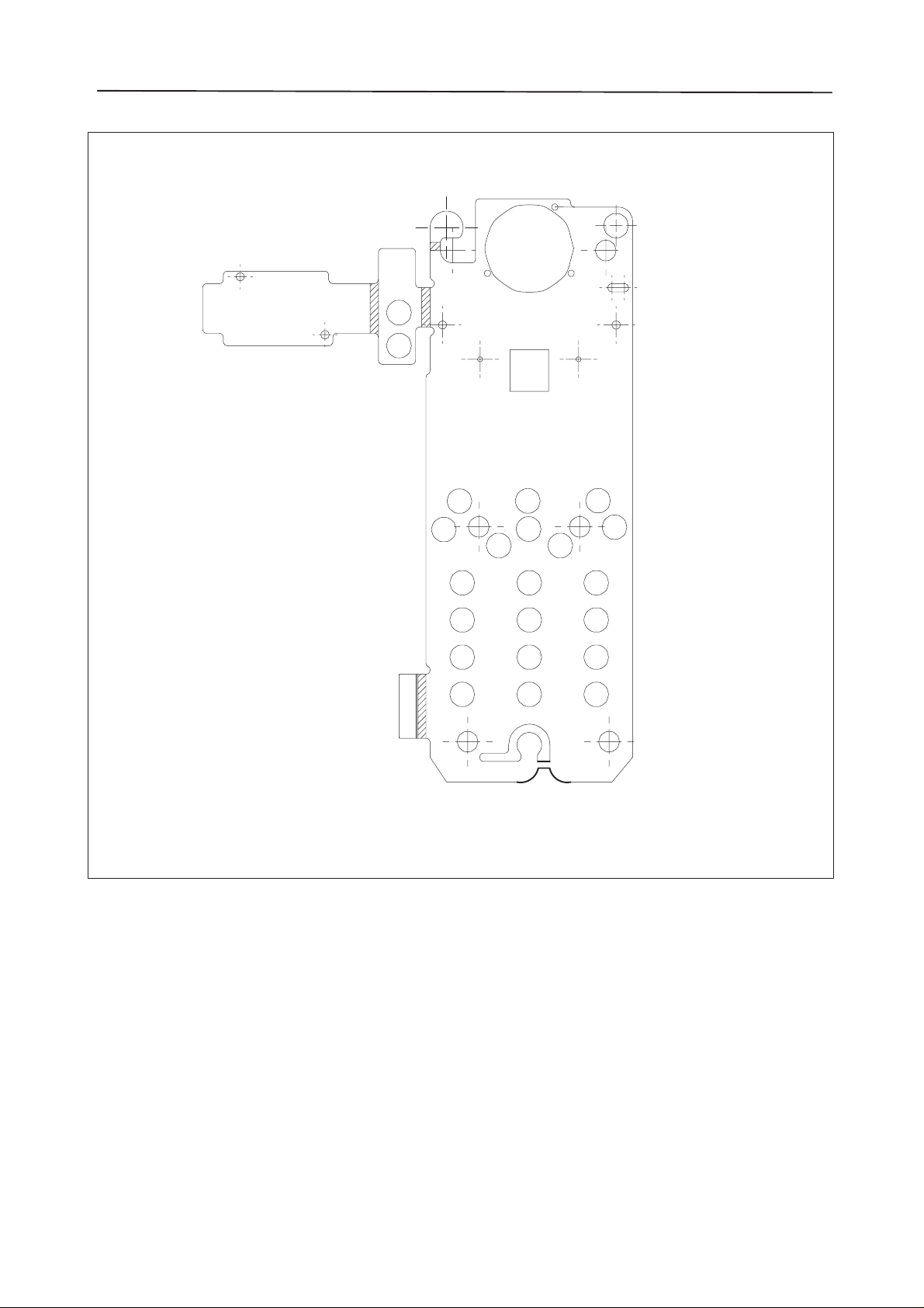
1
30
DU8C Style Flexi
Figure 1. Flexi Outline
The following sections of circuitry are on the flexi:
– Microphone Circuit
– Speaker Circuit
– LCD Display Module
– LCD voltage divider & temperature compensation circuit
– Keyboard & Display lighting circuits
– Keyboard switch matrix
– SIM Card Reader
Original 26/97
Page 5–4
Page 5
PAMS
Technical Documentation
UIF Module DU8
NHB–3
List of Submodules and Mechanical Parts
Module Submodule / Part Material code Notes
DU8C Euro/USA Display Module 4850038 Common part
DU8C Earphone Gasket 9450133 Common part
DU8C Lightguide Assembly 9460074 Common part
DU8C Mic Rubber 9460075 Common part
DU8C Reflector 9480061 Common part
DU8C Speaker Pad 9480062 Common part
DU8C Buzzer Gasket 9480078 Common part
DU8C Keydome Film Assembly 9795002 Main keyboard
DU8C Keydome Film Assembly 9795004 Power key (up right corner)
DU8C Keydome Film Assembly 9795006 Volume keys (side)
NOTE! All parts are common with DU8.
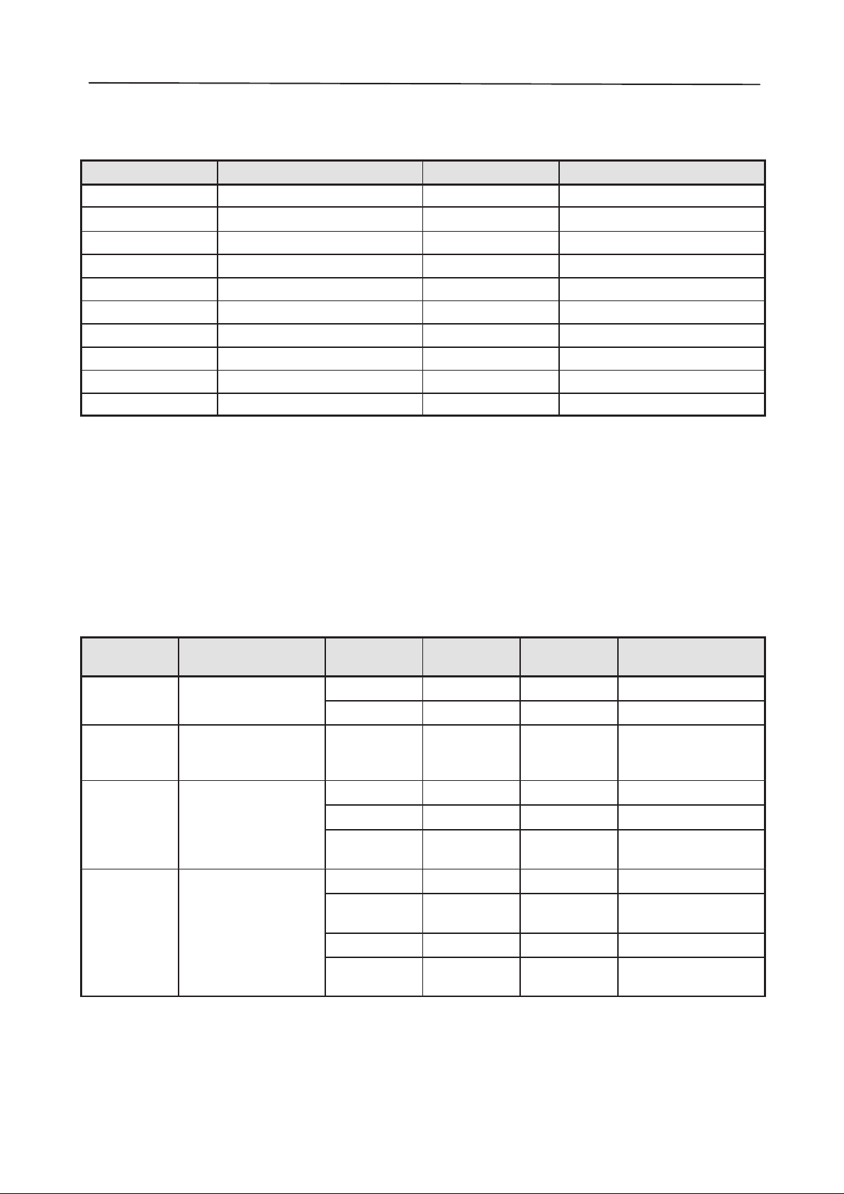
Technical Specifications
Maximum Ratings
DC Characteristics
Table 1. Supply Voltages and Power Consumption
Pin / Conn. Line Symbol Minimum Typical /
Nominal
1 / X4 VL1
24 / X4 VA1
3, 30 / X4 VBATT
4.5 4.65 4.8 V
1.5 mA LCD material B
0.8 mA LCD material D
4.5 4.65 4.8 V
250 uA mic enabled
25 mA max volume level to
5.3 6.0 9.0 V
85 mA 115 mA Buzzer with max vol-
40 mA Display illumination
Maximum Unit / Notes
(without temperature
compensation)
earphone
ume
Original 26/97
40 mA Keyboard illumina-
tion
Page 5–5
Page 6

PAMS
C
Technical Documentation
Control Signals
NHB–3
UIF Module DU8
Table 2. Control Signals
Pin / Conn. Line Symbol Minimum Typical /
Nominal
12 / X4 MIC_ENA
Mic_Enable
4 / X4 BACKLIGHT
Key and LCD light
17 / X4 CALL_LED
all indicator
25 / X4 SIMCLK 3.25 /1.625 MHz
26 / X4 SIMRESET
27 / X4 VSIM 4.5 4.65 5.5 V
28 / X4 SIMDATA
– 0 3 Volts Mic Enabled
VA1–0.4 VA1 VA1+3 Volts Mic Disabled
VA1–1.0 – VA1 V olts Lights On
0 – 2.0 Volts Lights Off
VA1–1.0 – VA1 V olts LED On
0 – 0.4 Volts LED Off
–0.3 0.6 V Low level
4.0 5.0 V High level
3.8 4.65 V High level
Maximum Unit / Notes
0.4 V Low level
AC Characteristics
Table 3. Audio Specifications
HPMIC 1 kHz rms NOTES
MRP pressure 2.8 dBPa 5 cm from MIC
MIC pressure –2.2 dBPa about 5 dB attenuation
MIC output 4.9 mV mic sensitivity –64 dB
0 dB = 1V/uBar 1uBar=0.1Pa
Codec gain 35 dB / 275 mV Codec maximum gain
Level – 8.5 dBmO 0 dBmO = 739 mV
HPEAR 1 kHz rms
Level – 6 dBmO / 245 mV 0 dBmO = 490 mV
Codec gain –3 dB 9 dB fixed gain – 12 dB atten.
Codec output 175 mV max. volume 435 mV (+12 dB)
Earpiece pressure 9 dBPa
Original 26/97
Page 5–6
Page 7

PAMS
Technical Documentation
Table 4. Other AC Specifications
BUZZER 2.7kHz Minimum Typical/Nominal Maximum NOTES
Buzzer 90 dB (S.P.L.) Level measured
UIF Module DU8
30 cm from
the buzzer with
pulse ratio 50/50
NHB–3
External Signals and Connections
Table 5. To Radio Module
Signal Name Pin / Conn. Notes
VL1 1 Logic supply voltage 4.65V
GND 2 Ground
VBATT 3, 30 Battery voltage
BACKLIGHT 4 Backlights on/off
UIF(0:6) 5 – 11 Lines for keyboard read and LCD–controller control
MIC_ENA 12 Microphone bias enable
COL(0:3) 13 – 16 Lines for keyboard write
CALL_LED 17 Call led enable
MICP 18 Microphone (positive node)
MICN 19 Microphone (negative node)
EARP 20 Earpiece (negative node)
EARN 21 Earpiece (positive node)
BUZZER 22 PWM signal buzzer control
XPWRON 23 Power key (active low)
VA1 24 Analog supply voltage 4.65V
SIMCLK 25 3.25 MHz Clock for SIM data
SIMRESET 26 Reset for SIM
VSIM 27 SIM voltage supply
SIMDATA 28 Serial data for SIM
AGND 29 Analog ground for the microphone
Original 26/97
Page 5–7
Page 8

PAMS
Technical Documentation
1
.
.
.
.
30
Figure 2. UIF Connections:
Order of Pin Numbering
Table 6. To LCD Module
Pin Signal Name Notes
1 GND Ground
NHB–3
UIF Module DU8
2,3 OSC1, OSC2 Oscillation terminals
4–8 V1–V5 LCD driving power source
9 V5OUT Negative voltage converter output
10–11 C1, C2 4.7 uF capacitor to generate negative volt-
age for the input voltage VCI
12 VCI Power source for voltage converter
13 VCC Power source
14 RS Register selection
15 R/W Read/write
16 EN Enable for read/write signal
17–20 D(0–3) Lower bits of 8 bit data bus, not used
21–24 D(4–7) 3–state 4 bit data bus
D7 also used for busy flag reading
Table 7. List of Connectors
Connector Name Code Notes Specifications / Ratings
X1 Display Module Connection.
X4 UIF Connector – FCB edge connector as de-
– FCB footprint for Display Mod-
ule
scribed above.
Refer to mentor footprint / Display Module Prodoc for pinout
30 connections at 0.5 mm
pitch
Original 26/97
Page 5–8
Page 9

PAMS
Technical Documentation
Mechanical Characteristics
Table 8. Mechanical Characteristics
NHB–3
UIF Module DU8
Module
Name
Bare Flexi circuit
DU8C
module
Dimensions (mm)
(W x H x D)
50 x 141 x 0.3mm except
in areas with partial thinning or thickening. (refer
to mechanical drawings for
more detail.
<3.6 deep at LCD
<4.2 deep at earpiece
<6.3 deep at buzzer
Functional Description
Circuit Description
DU8C Circuit Description
The module is connected with 30 pin flex connector to the system board, 24 pin
connector to the LCD module and 6 pin connector to the SIM card.
The module includes following main blocks:
Weight
(g)
5
22
– keyboard
– SIM interface
– illumination
– audio block
– LCD Module interface
Keyboard scanning and display driver control
COL(0–3) are used as column lines in keyboard. UIF(0–5) are used as row
lines. They are also multiplexed with display driver control signals.
When a key is pressed the ASIC gets an interrupt from a row and the MCU
starts scanning. One column at a time is written to low and rows are used to
read which key it was. The power off detection is multiplexed with one row;
when all keys on the row seems to be pressed the ASIC knows that power key
is pressed. The power key is also connected to PSL+ to switch the power on.
Row lines and UIF6 are used for display driver control. UIF(0–3) are used as 4
bit parallel data bus for the driver. UIF4 is used as read/write strobe, UIF5 to
select data or instruction register and UIF6 as enable strobe.
Keyboard and display illumination
The keyboard illumination is achieved by using two transistors wired as simple
constant current sinks. Each transistor supplies eight leds. The bases of the
Original 26/97
Page 5–9
Page 10

PAMS
Technical Documentation
transistors are all wired together and supplied by emitter follower V40. The led
current is fixed by the values of R44 and R45 and the ratio of R51 to R52. The
current is about 5 mA/ each LED. Note that on DU9 flexis, the 17
from an additional transistor.
The display illumination operates in a similar way to the keyboard drivers, two
transistors are used to drive eight leds. The current in this case is defined by
the value of R46, R47 and the ratio of R51 to R52. It is about 10 mA / each
LED.
The Call LED is fed from a simple emitter follower.
Audio Circuitry
The earpiece is routed directly via series resistors to connector X4. The earpiece is dynamic type. The impedance is 32 ohm and sensitivity 118 dB / 1 V.
Microphone is of the electret type and needs a voltage supply for operation.
When MIC_ENA is low bias voltage is connected to the microphone via transistor V8. V2 is wired as a switch for VA1, controlled by the microphone enable
line [MICENA]. VA1 is an analogue rail supplied by the PSL+ chip on the system board. It is 4.65V in magnitude. The sensitivity of the microphone is –62
dB (0 dB = 1V/ubar). C26 and C27 in the MIC nodes act as high pass filter with
pulldown resistors on the baseband side.–3dB point is about 100Hz.
NHB–3
UIF Module DU8
th
led is driven
The buzzer is dynamic one and the impedance is 25 ohm. Buzzer is driven
from a two transistor switch which acts as a buffer for a CMOS output signal
applied at BUZZER. The ringing volume is controlled by pulse width modulation.The diode V37 prevents damage to the transistor when switched off, absorbing the stored energy in the buzzer inductance and suppressing large positive going spikes on the transistor collectors.
Small value capacitors are fitted at critical points in the circuit to avoid problems
with RF interference. One is placed directly across the microphone (C15). V9
has a cap to ground from each of its three terminals (C14, C17 and C21).
There is also capasitors in earphone nodes.
LCD Module Interface
The LCD module includes the LCD and the display driver. The driver TAB is
connected with heat seal connection to the LCD. The LCD is FSTN type. The
duty ratio is 1/32 and the bias ratio 1/6.7. Viewing direction is 6 o‘clock.
The display driver is NJU6406–02 from JRC. It has internal clock oscillator and
negative voltage generator. It has 9600 bit character generator ROM and 64 * 8
bits character generator RAM. The dispaly module is connected to the UIF
module with 24 pin soldered connection.
The display module contains an oscillator to generate a negative voltage required for operation. The oscillator frequency is fixed on the UIF module by the
resistance from pins 2 to 3 of X1, with the values of R6 and R16 shown, the frequency is within 180 kHz to 370 kHz. The negative going pulses appear at pin 9
of X1 where they are smoothed by C1 to give a voltage which is nominally
equal but opposite to VL1.
Original 26/97
Page 5–10
Page 11

PAMS
Technical Documentation
For correct operation of the display, dc voltages between –VL1 and VL1 need
to be generated and fed back to the driver chip, at pins 4 to 8 inclusive (of X1).
The exact voltages depend on the relative values of the resistors R21, R37,
R38, R39, R40 and R33.
The display driver is connected to the radio module with a 4 bit data bus. Data
transfer is controlled with the following signals: R/W selects read or write operation (”0” = write, ”1” = read), Enable activates read/write operations and RS selects the register (”0” : instruction register (writing) or busy flag (reading), ”1” :
data register).
SIM interface
The SIM interface is the electrical interface between the smart card used in the
GSM and PCN applications and the MCU via the ASIC. Four signals are used
between the SIM card and the ASIC: SIMDATA, SIMCLK, SIMRESET and
VSIM. Serial data is transferred between the card and the ASIC, the clock frequency is 3.25 MHz. When there is no data transfer between the SIM card and
the HP the clock can be reduced to 1.625 MHz. Some cards allow to stop the
clock in that mode. The ASIC also generates the reset for the card and the supply voltage VSIM.
NHB–3
UIF Module DU8
Power Distribution Diagram
VA1
VL1
VSIM
VBATT
Call
LED
GND
AGND
KEY/
LCD
Lights
Figure 3. Power Distribution
Assembly
Buzzer
SIM card
reader
LCD
Keyboard
scan
Audio
Construction
The assembly drawings show the physical positioning of all the components on
the flexis.
Original 26/97
Page 5–11
Page 12

PAMS
Technical Documentation
The preassembled parts are the Display Module (LCD + TAB + Heatseal), KeyDome assemblies (Adhesive Film + Domes) and Lightguide/Reflector assembly
The basic assembly process is as follows:
– All SMD components placed & soldered.
– KeyDome assemblies fitted by hand (alignment jig recommended) (3 as-
semblies in DU8)
– Buzzer soldered manually
– Microphone soldered manually
– Speaker wires soldered manually
– Speaker attached to flexi with speaker pad
– Speaker gasket attached to top of speaker (self–adhesive)
– Display Module soldered to flexi (alignment pins required)
– Light guide/reflector assembly stuck onto the flexi over the TAB package
– LCD folded on to the top of the light guide and stuck down
– Functional tests performed.
Limited Bending Capability:
tion of three layers of polyimide and two layers of copper tracks. The polyimide
has almost unlimited bending capability – but the copper tracks cannot be bent
to tight radii very often. At all times before the flexi circuit is installed into a
phone, bending of the circuit should be avoided if possible. If the flexi circuit
has already been installed into the phone, then care should be taken not to
continuously fold the flexi circuit out flat and then back to its resting position too
often.
NHB–3
UIF Module DU8
The flexible circuits are constructed from a lamina-
Table 9. References to Other Construction Documents
Document Code Sheets Notes
Flexi outline 2D22779 1 Mechanical Outline Drawing
Assembly Description
Table 10. References to Other Assembly Documents
Document Drawing n:o Sheets Notes
Flexi assembly for DU8C 2C23369 1 Common with DU8 Assembly Drawing
Original 26/97
Page 5–12
Page 13

PAMS
Technical Documentation
Flexi Assembly for UIF Module DU8
NHB–3
UIF Module DU8
Original 26/97
Page 5–13
Page 14

PAMS
Technical Documentation
UIF Module DU8
Assembly Parts of UIF Module DU8
ITEM Q’TY CODE DESCRIPTION VALUE, TYPE
1 1 9855011 F.P.C. . . . . . . . . . . .
2 1 4850038 Display Module . . . . . . . . . . . .
3 1 9460074 Lightguide. . . . . . . . . . . .
4 1 9480061 Reflect. . . . . . . . . . . .
5 1 9795002 Keydome Film. . . . . . . . . . . .
6 1 9795006 Keydome Side. . . . . . . . . . . .
7 1 9480078 Buzzer Gasket. . . . . . . . . . . .
8 1 514H001 Earpiece. . . . . . . . . . . .
9 1 9450133 Speaker Gasket. . . . . . . . . . . .
10 1 9480062 Speaker Pad. . . . . . . . . . .
11 1 9460075 Microphone Rubber. . . . . . . . . . .
12 1 514H002 Microphone. . . . . . . . . . .
13 1 514H003 Buzzer. . . . . . . . . . .
14 1 9795004 Keydome Pwr. . . . . . . . . . .
NHB–3
T esting
Recommended Test Equipment
Radio Modules db1 and db6.
Test Procedure
1 Connect the UIF module to the radio module and place a SIM card to
the card reader of the flex.
2 Connect a battery to the battery connector.
3 Switch the power on and check that all the segments of the LCD are
displayed.
4 Verify that all keyboard and LCD backlight leds are illuminated.
5 Verify that the SIM card is accepted.
6 Press all keys and verify that all keypresses can be detected.
7 Verify that the earpiece is generating a tone during a keypress.
8 Make a call to the tranceiver.
9 Verify that the ringing tones are coming from the buzzer.
Original 26/97
10 Verify that the call led is illuminated.
11 Answer the call.
12 Verify that the microphone is working.
Page 5–14
 Loading...