

Page 1

Programmes After Market Services (PAMS)
Technical Documentation
NHB–3 Series Transceiver
Chapter 4
SYSTEM MODULE
Page 2

PAMS
Technical Documentation
CHAPTER 4 – SYSTEM MODULE
CONTENTS
System Module DB6 4–4
Baseband Block 4–4
Introduction 4–4
Technical Summary 4–4
Interconnection Diagram 4–5
Technical Specifications 4–5
Control Signals 4–6
Connector to UIF Module 4–9
System Connector X100 4–10
Internal Signals and Connections 4–11
Functional Description 4–13
Clocking Scheme Diagram 4–13
Circuit Description 4–13
Reset and Power Control Diagram 4–14
Watchdog System Diagram 4–15
Power Distribution Diagram 4–16
CTRLU 4–17
PWRU 4–21
Introduction 4–21
Block Description 4–22
DSPU 4–24
Introduction 4–24
Technical Description 4–26
Block Description 4–27
AUDIO 4–28
Introduction 4–28
Technical Specification 4–28
Block Description 4–29
ASIC 4–31
Introduction 4–31
Technical Specification 4–31
Block Description 4–33
RFI 4–36
Introduction 4–36
Technical Specification 4–36
Block Description 4–37
Definitions and Abbreviations 4–38
NHB–3
System Module DB6
Page No
Original 26/97
Page 4–2
Page 3

PAMS
Technical Documentation
RF Blocks 4–39
Technical Summary 4–39
Technical Specification 4–39
Power Distribution Diagram 4–39
Functional Description 4–41
RF Characteristics 4–42
Transmitter 4–44
Synthesizer 4–45
Block Diagram of Receiver Section 4–46
Connections between RX and TX (Version: 6.0 Edit: 88) 4–47
Block Diagram 4–48
Block Diagram of System Section 4–49
Circuit Diagram of CTRLU Section 4–50
Circuit Diagram of PWRU Section 4–51
Circuit Diagram of DSPU Section 4–52
Circuit Diagram of Audio Section 4–53
Circuit Diagram of ASIC Section 4–54
Circuit Diagram of RFI Section 4–55
Circuit Diagram of Receiver Section 4–56
Circuit Diagram of Transmitter Section 4–57
Component Layout Diagram of DB6 side 1 4–58
Component Layout Diagram of DB6 side 2 4–59
Parts List of DB6 (EDMS Issue: 3.1) 4–60
NHB–3
System Module DB6
Original 26/97
Page 4–3
Page 4

PAMS
Technical Documentation
System Module DB6
Baseband Block
Introduction
The baseband block is designed for a handportable phone, that operates in the
DCS1900 system. The purpose of the baseband module is to control the phone
and process audio signals to and from the RF block. The module also controls
the user interface.
Technical Summary
All functional baseband blocks are mounted on a single 6–layer printed circuit
board. This board contains also RF parts. The chassis of the radio unit has
separating walls for baseband and RF. All components of the baseband section
are surface mountable. They are soldered using reflow. The connections to accessories are taken through the bottom connector of the radio unit. The connections to the User Interface module (UIF) are fed through a flex connector.
There is no physical connector between the RF and baseband sections.
NHB–3
System Module DB6
List of submodules:
CTRLU Control Unit for the phone
PWRU Power supply
DSPU Digital Signal Processing block
AUDIO Audio coding
ASIC D2CA GSM/PCN ASIC
RFI RF – baseband interface
The blocks above are only functional blocks and therefore have no type or material codes.
Original 26/97
Page 4–4
Page 5
PAMS
Technical Documentation
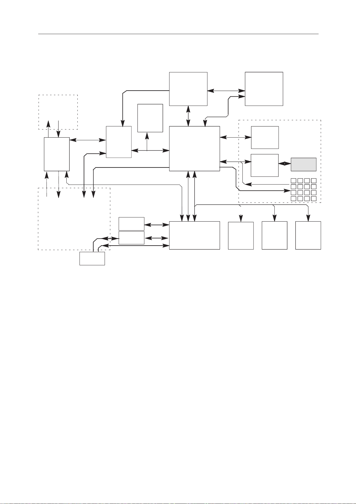
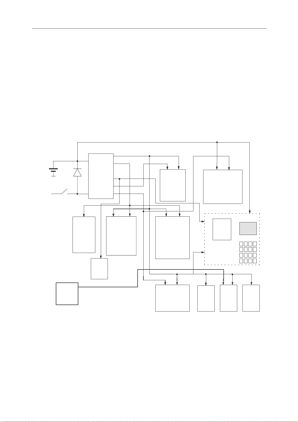
Interconnection Diagram
NHB–3
System Module DB6
UIF–module
mic
ear
sio
AUDIO
xearxmic
System
connector
dbus
FLASH
LOAD
RFI
12 bit parallel +
32K x 16
SRAM
sio
DSP
ext
sio
mem
PSL+
CHRGR
M2 BUS
Interface
A14:0,
D15:0
A5:0,
D15:0
sio
8 x control
ASIC
A4:0
A19:16
D7:0
A19:0,D7:0
ext mem
io
io
io
MCU
A12:0,D7:0
E2PROM
8K X 8
RF
UIF–module
UIM CARD
READER
LCD
DRIVER
A17:0,D7:0
1024K x 8
FLASH
LCD
LCD
A14:0,D7:0
32K x 8
SRAM
sio
Technical Specifications
Modes of Operation
There are four different operation modes
– active mode
– idle mode
– power off mode
– local mode
In the active state all circuits are powered and part of the module may be in idle
mode.
The module is usually in the idle mode when there is no call and the phone is in
SERV. In the idle mode circuits are reset, powered down and clocks are
stopped or the frequency reduced. All the clocks except the main clock from
VCTCXO can be stopped in that mode. Whether the UIM clock is stopped or
not depends on the network and UIM card type.
Original 26/97
Page 4–5
Page 6

PAMS
Technical Documentation
In power off mode only the circuits needed for power up are powered. This
means that only power up block inside the PSL+ is powered. The power key on
the flex is pulled up with a pull up resistor inside the PSL+.
The local mode is used for alignment and testing.
Supply Voltages and Power Consumption
Pin/Conn. Symbol Notes
VBATT/sys VBATT • min/typ/max 5.3 /6.0 /8.6 V sw limit
• min/typ/max 4.5 /6.0 /8.9±0.3 V hw limit
• min/typ/max 4.5 /6.0 /7.3±0.3 V hw limit
during a call
VA1 • min/typ/max 4.5 / 4.65 /4.8 V Imax = 40 mA
VA2 • min/typ/max 4.5 / 4.65 /4.8 V Imax = 80 mA
VL1 • min/typ/max 4.5 / 4.65 /4.8 V Imax = 150 mA
NHB–3
System Module DB6
14/sys VF • min/typ/max 11.4 /12 /12.6 V Flash
8,16/sys VCHAR • min/typ/max 10 /12 /13.5 V Charger voltage,
Control Signals
Pin/Con Symbol Notes
5/sys M2BUS • min/max 0 /0.7 V Input low level
6/sys HOOK_RXD2 • Connected to MCU A/D input
VL2 • min/typ/max 4.5 / 4.65 /4.8 V Imax = 150 mA
VREF • min/typ/max 4.55 / 4.65 /4.75 V Imax = 5 mA
programming voltage
when Isink<730 mA
• min/typ/max 730 /800 /870 mA Charger cur–
rent, when Uin<10 V
• min/max 3.0 /4.8 V Input high level
• min/typ/max 0 /0.2 /0.35 V Output low level
• min/typ/max 3.6 /4.65 /4.8V Output high level
• min/typ/max 4.1 /4.65 /4.8 V (not in use)
• min/typ/max 3.0 /3.45 /4.0 V Headset
adapter and plug are connected
• min/typ/max 1.9 /2.35 /2.9 V Hook off in
compact HF
• min/typ/max 0 /0.5 /0.7 V Hook on in
compact HF
Original 26/97
Page 4–6
Page 7

PAMS
Technical Documentation
Pin/Con Symbol Notes
6/sys HOOK_RXD2 • Flash loading data
7/sys PHFS TXD2 • Power control for PHF–1
15/sys DCLK • DBUS clock 512 kHz
NHB–3
System Module DB6
• min/typ/max 0 /0.2 /0.7 V Input low level
• min/typ/max 3.6 /4.65 /4.8 V Input high level
• min/typ/max 0 /0.2 /0.7 V Output low,
power off
• min/typ/max 3.6 /4.65 /4.8 V Output high,
power on
• Flash loading acknowledgedata
• min/typ/max 0 /0.2 /0.7 V Output low level
• min/typ/max 3.6 /4.65/4.8 V Output high level
• min/typ/max 3.6 /4.65 /4.8 V State ”1”
• min/typ/max 0 /0.2 /0.7 V State ”0”
11/sys DSYNC • DBUS sync 8 kHz
• min/typ/max 3.6 /4.65 /4.8 V State ”1”
• min/typ/max 0 /0.2 /0.7 V State ”0”
4/sys TDA • DBUS transmitted data from HP
• min/typ/max 3.6/4.65/4.8 V State ”1”,
1mA load
• min/typ/max 0 /0.2 /0.7 V State ”0”
12/sys RDA • DBUS received data to HP
min/typ/max 3.6/4.65/4.8 V State ”1”
• min/typ/max 0 /0.2 /0.7 V State ”0”
13/sys BENA • typ 0 V Headset power off
• min/typ 4.4 /4.6 V Headset power on
4/UIF BACKLIGHT • Display and keyboard illumination control
• min/max 0 /0.7 V Output low, backlights off
• min/typ/max 4.5 /4.65 / 4.8 V Output high,
backlights on
5–8/UIF UIF(0:3) • Keyboard row lines read. Display data
lines write.
• min/max 0 /0.7 V Output/Input low
• min/max 4.5 /4.8 V Output/Input high
9/UIF UIF4 • Keyboard row read. Write strobe for
Original 26/97
LCD driver
• min/max 0 /0.7 V Output/Input low
• min/max 4.5 /4.8 V Output/Input high
Page 4–7
Page 8

PAMS
Technical Documentation
Pin/Con Symbol Notes
10/UIF UIF5 • Keyboard row read. LCD driver register select
11/UIF UIF6 • Enable strobe for LCD driver
12/UIF MIC ENA • min/max 0 /0.7 V Output low,
13–16/ COL(0:3) • Keyboard columns
UIF • min/max 0 /0.7 V Output low
17/UIF CALL LED • min/max 0 /0.7 V Output low, call led off
NHB–3
System Module DB6
• min/max 0 /0.7 V Output/Input low
• min/max 4.5 /4.8 V Output/Input high
• min/max 0 /0.7 V Output/Input low
• min/max 4.5 /4.8 V Output/Input high
microphone bias on
• Floating, microphone off
• min/max 4.5 /4.8 V Output high
• min/typ/max 4.5/ 4.65/ 4.8 V Output high,
call led on
22/UIF BUZZER • PWM output from MCU
• min/max 0 /0.7 V Output low, buzzer off
• min/typ/max 4.5/ 4.65/ 4.8 V Output high,
buzzer on
23/UIF XPWRON • min/typ/max 0 /0 /0.7 V Input low,
power on/off
• typ 4.65 V Floating when inactive.
A pull–up in PSL+
25/UIF UIMCLK • Clock for UIM card
• min/typ/max 3.6 /4.65 /4.8 V State ”1”
• min/typ/max 0 /0.2 /0.7 V State ”0”
• min/max 1 MHz /5 MHz UIM card
clock frequency
26/UIF UIMRESET • Reset for UIM card
• min/typ/max 4.5/ 4.65/ 4.8 V Output high
• min/max 0 /0.7 V Output low
27/UIF VUIM • min/typ/max 4.5/ 4.65/ 4.8 V UIM card reader
supply voltage
• max 10 mA UIM card supply current at
any frequency
• max 100 µA UIM card supply current in
idle state at 1 MHz and 25°C
28/UIF UIMDATA • Data for UIM card In/Out
Original 26/97
• min/typ/max 3.6 /4.65 /4.8 V State ”1”
• min/typ/max 0 /0.2 /0.7 V State ”0”
Page 4–8
Page 9

PAMS
Technical Documentation
Pin/Con Symbol Notes
BTYPE/ BTYPE • A pullup in phone. 47 kΩ resistor series with
sys 100 kΩ resistor and transitor C–E paraller
NHB–3
System Module DB6
connection
• min/typ/max 0.88 /0.98 /1.09 V
400mAh/15kΩ (pull resistor in the battery pack)
• min/typ/max 1.02 /1.13 /1.25 V 500 mA/18kΩ
• min/typ/max 1.86 /2.02 /2.20 V 950 mA/47kΩ
battery don‘t be in accessorylist
• min/typ/max 2.03 /2.20 /2.37 V,
1100 mAh/56 kΩ
• min/typ/max 2.22 /2.39 /2.58 V,
1200 mAh/68 kΩ battery don‘t be in access.list
• min/typ/max 2.58 /2.76 /2.95 V,
1500 mAh/100 kΩ
• min/typ/max 3.30 /3.48 /3.66 V,
Lithium/270 kΩ,battery don‘t be in access.list
• min/typ/max 1.02 /1.13 /1.25 V,
Vibra 500 mAh/18 kΩ
BTEMP/ TBAT • A 100 kΩ pull–up resistor in HP
sys • typ 3.49 V , at – 5 C
Connector to UIF Module
Signal name Pin Notes
VL1 1 Logic supply voltage 4.65V
GND 2 Ground
VBATT 3,30 Battery voltage
BACKLIGHT 4 Backlights on/off
UIF(0:3) 5–8 Lines for keyboard read and LCD–controller
• typ 2.97 V , at +5 C,Battery temperature
cold limit
• typ 2.86 V , at +7 C
• typ 1.23 V , at +40 C
• typ 0.97 V , at +48 C, Battery temperature
hot limit
• Vibra Battery control. PWM output from
MCU. DC separated.
data
UIF4 9 Line for keyboard read and LCD–controller
Original 26/97
read/write strobe
Page 4–9
Page 10

PAMS
Technical Documentation
Signal name Pin Notes
UIF5 10 Line for keyboard read and LCD–controller
UIF6 11 LCD–controller enable strobe
MIC_ENA 12 Microphone bias enable
COL(0:3) 13–16 Lines for keyboard write
CALL_LED 17 Call led enable
MICP 18 Microphone (positive node)
MICN 19 Microphone (negative node)
EARP 20 Earpiece (negative node)
EARN 21 Earpiece (positive node)
BUZZER 22 PWM signal buzzer control
XPWRNON 23 Power key (active low)
NHB–3
System Module DB6
data/instruction register selection
VA1 24 Analog supply voltage 4.65V
UIMCLK 25 Clock for UIM data
UIMRESET 26 Reset for UIM
VUIM 27 UIM voltage supply
UIMDATA 28 Serial data for UIM
GND 29 Analog ground. Connected directly to digital
System Connector X100
Signal name pin Notes
GND 1,9 Digital ground.
MIC_JCONN 2 External audio input from accessories or
AGND 3 Analog ground for accessories.
ground on the PCB.
handsfree microphone. Multiplexed with
junction box connection indication. 16.8k
pull down in HP
Connected directly to digital ground on
the PCB.
TDA 4 Transmitted DBUS–data to the accessories
M2BUS 5 Serial bidirectional data and control between
Original 26/97
the handphone and accessories.
Page 4–10
Page 11

PAMS
Technical Documentation
Signal name Pin Notes
HOOK_RXD2 6 HOOK–indication. The phone has a 100k
PHFS_TXD2 7 Hands–free device power on/off. Data to flash
VCHAR 8,16 Battery charging voltage.
EAR_HFPWR 10 External audio output to accessories or
DSYNC 11 DBUS–data bit sync clock.
RDA 12 DBUS received data from the accessories.
BENA 13 Power supply to headset adapter.
VF 14 Programming voltage for flash from Flash box.
NHB–3
System Module DB6
pull–up resistor. Data to flash from flash
programmer.
programming device.
handsfree speaker. 100kW pull–down in HP to
turn on the junction box.
DCLK 15 DBUS–data clock.
GND BGND Ground
TBAT BTEMP Battery temperature and vibrabattery control
BTYPE BTYPE Battery type
VBATT B+ Battery voltage
VCHAR DC+ Battery charging voltage
VCHAR CH+ Battery charging voltage
GND GND Charging ground, also phone ground
Internal Signals and Connections
Signals between RF and ASIC
Signal Name Function Notes
SCLK Synthesizer clock ASIC–>RF
SDATA Synthesizer data ASIC–>RF
SENA1 Synthesizer enable, UHF and ASIC–>RF
RXPWR RX supply voltage ON/OFF ASIC–>RF
SYNTHPWR Synthesizer supply voltage ON/OFF ASIC–>RF
TXPWR TX supply voltage ON/OFF ASIC–>RF
TXP Transmitter power control enable ASIC–>RF
Original 26/97
VHF PLL enable
Page 4–11
Page 12

PAMS
Technical Documentation
Signal Name Function Notes
TXL Transmitter low power enable, ASIC–>RF
RFC 26 MHz clock to ASIC CLKIN RF –> ASIC
Signals between RF and RFI
Signal Name Functions Notes
AFC Automatic frequency control voltage RFI –> RF
TXC TX transmit power control voltage, RFI –> RF
TXQP,TXQN differential TX quadrature signal RFI –> RF
TXIP,TXIN differential TX inphase signal RFI –> RF
PDATA0 front end AGC control RFI –> RF
NHB–3
System Module DB6
”0” = low power, ”1” = normal power
AGC control in receiving
RXQ RX quadrature signal RF –> RFI
RXI RX inphase signal RF –> RFI
Signals between RF and CTRLU
Signals name Function Notes
TRF RF temperature RF –> CTRLU
Original 26/97
Page 4–12
Page 13
PAMS
Technical Documentation
Functional Description
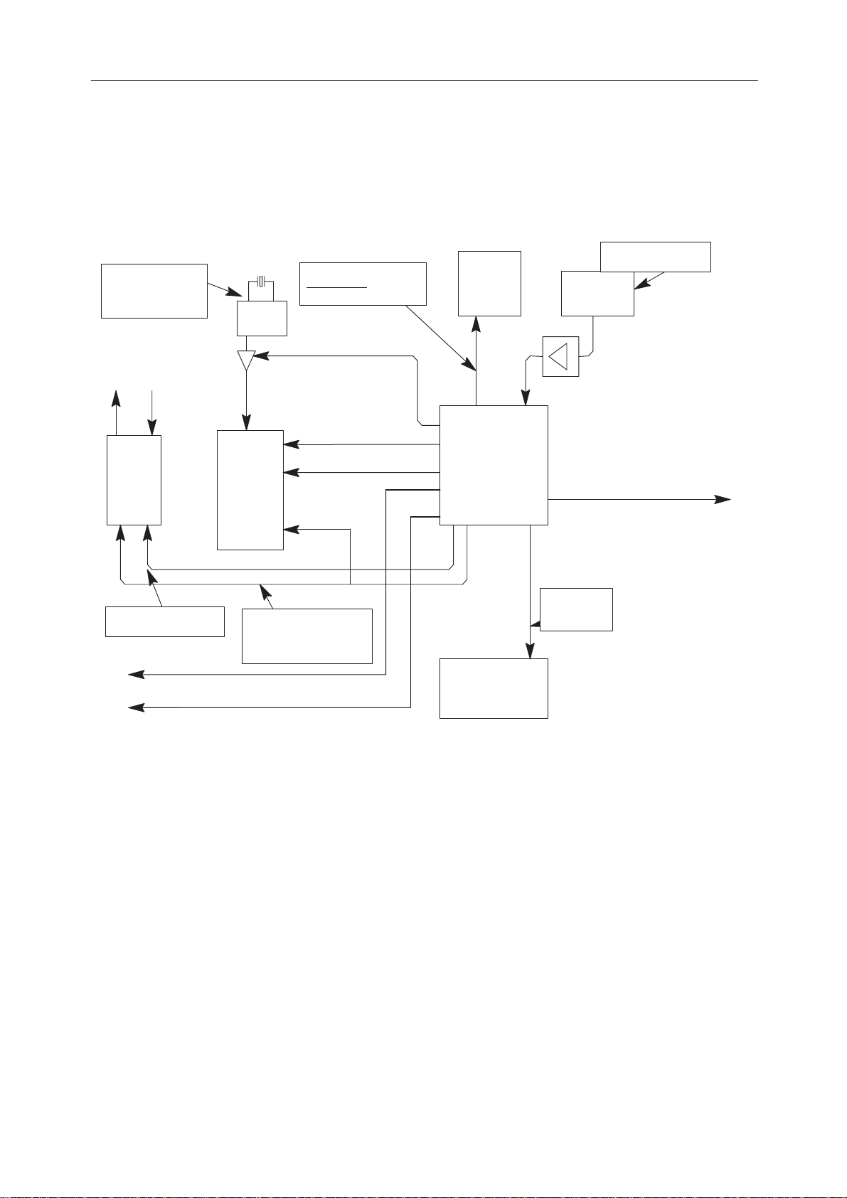
Clocking Scheme Diagram
DSP Clock
60.2 MHz
differential sine
wave
ear
mouth
OSCIL–
LATOR
RFI Clock 13 MHz
Sleep Mode:
135.4kHz
DBUSCLK 512kHz
enable
RFI
NHB–3
System Module DB6
RF System Clock
26 MHz
VCTCXO
AUDIO
CODEC
Codec Sync Clock
8 kHz
DBUSCLK 512kHz
DBUSSYNC 8kHz
DSP
Circuit Description
Most of the clocks are generated from the 26 MHz VCTCXO frequency by the
ASIC:
– 26 MHz clock for the MCU. MCU‘s internal clock frequency is half
of that (13 MHz).
DBUSSYNC 8kHz
Codec Main Clock
and data Transfer
clock
512kHz
ASIC
UIMCLK
3.25 / 1.625
MHz
MCU
Clock
26 MHz
MCU
Original 26/97
– 13 MHz for the RFI. The ASIC also generates 135.4 kHz sleep
mode clock for the RFI.
– 3.25 MHz clock for UIM. When there is no data transfer between
the UIM card and the HP the clock can be reduced to 1.625 MHz.
Some UIM cards also allows the clock to be stopped in that mode.
– 512 kHz main clock for the codec and for the data transfer between the DSP and the codec.
Page 4–13
Page 14
PAMS
Technical Documentation
– 8 kHz syncronisation clock for data transfer between the DSP and
the codec.
– 512 kHz clock and 8 kHz sync. clock for the DBUS data transfer.
The DSP has its own crystal oscillator which can be turned off and on by the
ASIC. The DSP uses differential sinusoidal clock. The frequency is 60.2 MHz.
The MCU generates 8 kHz clock to the codec for the control data transfer.
In the idle mode all the clocks can be stopped except 26 MHz main clock com-
ing from the VCTCXO.
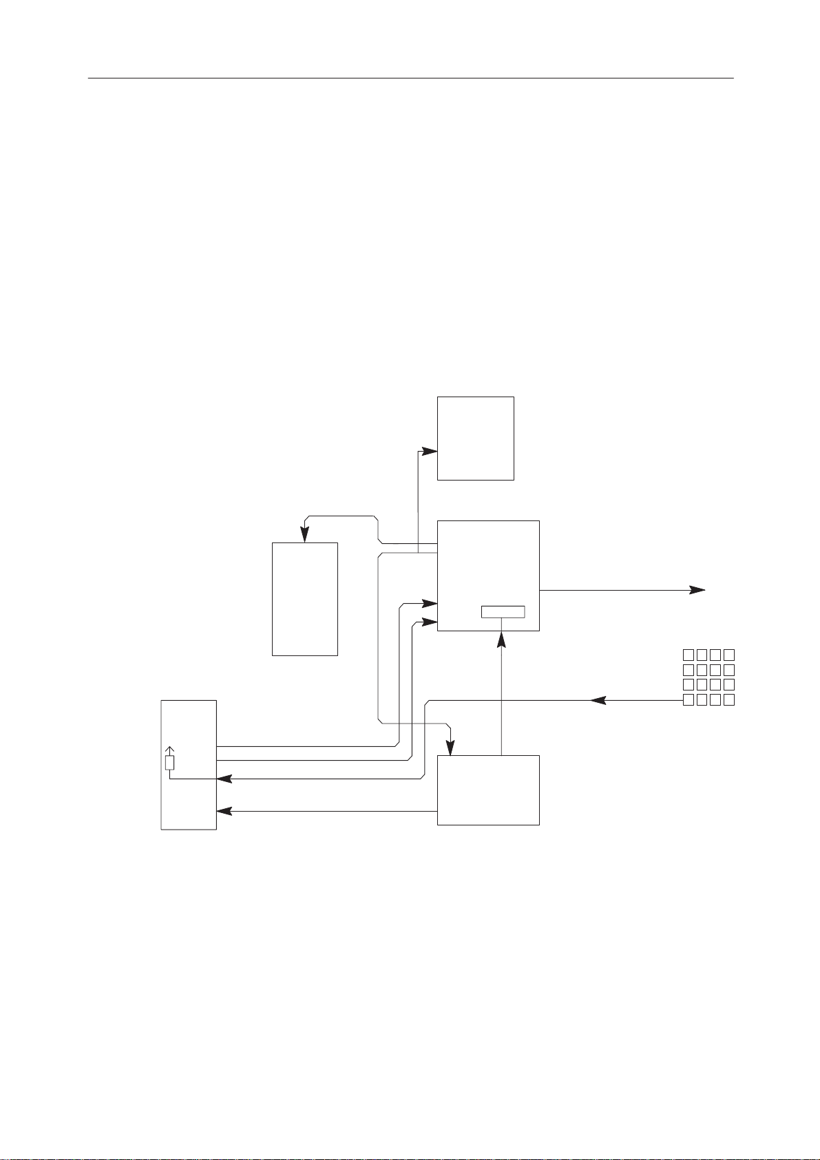
Reset and Power Control Diagram
NHB–3
System Module DB6
RFI
PSL+
VL1
XRES reset in
XPWRON
XPwrOff
Circuit Description
There are three different ways to switch power on:
reset in
DSP
approx 2Hz
Reset Out
Reset Out
ASIC
Vcc
Reset in
MCU
UIMRESET
resetreg
XPWRON
– Power key pressing grounds the XPWRON line. The PSL+ detects
that and switches the power on.
Original 26/97
– Charger detection on PSL+ detects that charger is connected and
switches power on.
Page 4–14
Page 15
PAMS
Technical Documentation
– PSL+ will switch power on when the battery is connected. After
that the MCU will detect if power key is pressed or charger connected. If not the power will be switched off.
All devices are powered up at the same time by the PSL+. It supplies the reset
to the ASIC at power up. The ASIC starts the clocks to the DSP and the MCU.
After about 20us the ASIC releases the resets to MCU, RFI and DSP. MCU
and RFI reset is released after 256 13 MHz clock cycles. DSP reset release
time from DSP clock activation can be selected from 0 to 255 13MHz clock
cycles. In our case it is 255. UIM reset release time is according to DSC1900
UIM specifications.
To turn off power for the phone, the user presses the PWR key. The MCU detects this. The MCU cuts off any ongoing call, exits all tasks, acts inoperative to
the user and leaves the PSL+ watchdog without resets. After power–down
delay, the PSL+ cuts off the supply from all circuitry.
If charging is on the phone stays on but it looks to the user like it is powered off
(lights are off and the display is blank) except the charging indicator stays on.
NHB–3
System Module DB6
Watchdog System Diagram
PSL
reset
DSP
5
POWER
4
ASIC
1
2
3
reset
4
Original 26/97
MCU
XPWROFF
Page 4–15
Page 16
PAMS
Technical Documentation
Circuit Description
Normal operation:
1. MCU tests DSP
2. MCU updates ASIC watchdog timer (> 2Hz)
3. MCU pulses the XPWROFF input on the PSL+ (about 2Hz)
Failed operation:
4. ASIC resets MCU and DSP after about 0.5 s failure
5. PSL+ switches power off about1.5 s after the previous XPWROFF pulse
Power Distribution Diagram
PSL+
VBATT
VL1
VL2
NHB–3
System Module DB6
VCHAR
FLASH
BOX
VF
VL2
32Kx1
6
SRAM
VA1
PCM
CODE
C
VA1
VA2
VREF
VL1
DSP
VL2
VA2 VL1
RFI
VL1
VL2
ASIC
VREFVL1
MCU
MCU
VBATT VREF
VA1
LCD Driver
VL1
VL1
E2PROM
8K x 8
RF
UIF–module
UIF–module
VBATT
VL1
VF
512K x
8
FLASH
LCD
LCD
VL1
32K x
8
SRAM
Circuit Description
PSL+ control supply voltages. VL1 and VL2 are supply voltages to the logic circuits. VA1 and VA2 are supply voltages to the audio circuits. VREF is A/D converter and RF reference voltage. VBATT is fed directly to the circuits which
need higher operation voltage and more current like RF transmitter and UIF
backlight. VF is flash programming voltage, which is fed from flash box.
PSL+ output voltages are active, when PSL+ is in power on state.
Original 26/97
Page 4–16
Page 17

PAMS
Technical Documentation
CTRLU
Introduction
The Control block contains a microcomputer unit (MCU) and three memory circuits (FLASH, SRAM, EEPROM), a 20–bit address bus and an 8–bit data bus.
Main Features of the CTRLU Block
MCU functions:
– system control
– communication control
– user interface functions
– authentication
– RF monitoring
– power up/down control
– accessory monitoring
– battery monitoring and charging control
– self–test and production testing
– flash loading
NHB–3
System Module DB6
External Signals and Connections, Inputs
Signal name Signal description From
VL1 Power supply voltage for CTRLU block PWRU
VREF Reference voltage for MCU AD–converter PWRU
VBATDET Battery voltage detection PWRU
VC Charger voltage monitoring PWRU
EROMSELX Chip select for the EEPROM memory ASIC
ROMSELX Chip select for the FLASH memory ASIC
RAMSELX Chip select for the SRAM memory ASIC
RESETX Reset signal for MCU ASIC
NMI Non–maskable interrupt request ASIC
MCUCLK Main clock for MCU ASIC
IRQX Interrupt request ASIC
PCMCDO Audio codec control data receiving AUDIO
TRF RF–module temperature detection RF
VF Programming voltage for flash memory system con.
HOOK_RXD2 The use of handsfree monitoring. Flash system con.
Original 26/97
programming data input on the production
line.
Page 4–17
Page 18

PAMS
Technical Documentation
Signal name Signal description From
TBAT Battery temperature detection and system con.
vibrabattery control
BTYPE Battery size identification system con.
JCONN Junction box connection identification AUDIO
ROMAD18 Rom address 18, (paging) ASIC
External Signals and Connections, Outputs
Signal name Signal description To
XPWROFF Power off control, PSL+ watchdog reset PWRU
PWM Charger on/off control PWRU
WSTROBEX MCU write strobe ASIC
RSTROBEX MCU read strobe ASIC
NHB–3
System Module DB6
MCUAD(19:0) 20–bit MCU address bus ASIC
MBUSDET MBUS activity detection ASIC
PCMCLK Clock for audio codec control data AUDIO
transfer
PCMCDI Audio codec control data transmitting AUDIO
XSELPCMC Chip select for audio codec AUDIO
PHFS_TXD2 Power on/off control for HF device. system con.
Verification output of the programmed data
of FLASH during programming.
CALL_LED ’Incoming’ call indicator light control UIF conn.
BACKLIGHT LCD and display backlight on/off control UIF conn.
BUZZER Buzzer signal UIF conn.
VOLTUM Software charging voltage limit PWRU
BATDET Detect battery removing and give to ASIC ASIC
warning, ASIC drive UIM card down
External Signals and Connections, Bidirectional
Signal name Signal description To/From
MCUDA(7:0) MCU‘s 8–bit data bus ASIC
M2BUS Asynchronous serial data bus system conn.
Original 26/97
Page 4–18
Page 19

PAMS
Technical Documentation
Block Description
MCU – Memories:
The MCU has a 20 bits wide address bus A(19:0) and an 8–bit data
bus with memories. The address bits A(19:16) are used for chip select decoding. The decoding is done in the D2CA ASIC. The ASIC
can address two 4 Mbit (or smaller) or one 8 Mbit flash memories.
Hitachi HD647536 processor has 60kbyte internal ROM and 2kbyte
RAM memories. One wait state is used in flash memory access.
Flash programming
In flash programming a special flash programming box and a PC is
needed. Loading is done through the bottom connector of HP; multiplexed with HOOK_RXD2 and PHFS_TXD2 line. First MCU goes to
minimum mode (MBUS command from PC or if MBUS is connected
to MIC_JCONN line in power up). Then the flash software is loaded
from PC to flash loading box. When the loading is complete flash
loading to HP can be started by MBUS command from PC to the
MCU. After that the MCU asks the test box to start flash loading to
HP. The box supplies 12 V programming voltage for flash and starts
to send 250 bytes data blocks to the MCU via HOOK_RXD2 line.
The baud rate is 406 kbit/s. The MCU calculates the check sum,
sends acknowledge via PHFS_TXD2 line and sends the data to
flash. When all the data is loaded the HP makes reset and tells the
flash loading box if the loading was succeeded or not. Only PSL+,
ASIC and MCU must be active during the loading.
NHB–3
System Module DB6
CTRLU – PWRU
MCU controls the watchdog timer in PSL+. It sends a positive pulse
at approximately 2 Hz to XPWROFF pin of the PSL+ to keep the
power on. If MCU fails to deliver this pulse, the PSL+ will remove
power from the system. MCU also controls the charger on/off switching in the PWRU block. When power off is requested or MCU leaves
PSL+ watchdog without reset. After the watchdog time has elapsed
PSL+ cuts off the supply voltages from the phone.
CTRLU – ASIC
MCU and ASIC have a common 8–bit data bus and a 9–bit address
bus. Bits A(4:0) are used for normal addressing whereas bits
A(19:16) are decoded in ASIC to chip select inputs for CTRLU memories. ASIC controls the main clock, main reset and interrupts to
MCU. The internal clock of MCU is half the MCUCLK clock speed.
RESETX resets everything in MCU except the contents of the RAM.
IRQX is a general purpose interrupt request line from ASIC. After
IRQX request the interrupt register of the ASIC is read to find out the
reason for interrupt. NMI interrupt is used only to wake up MCU from
software standby mode.
Original 26/97
Page 4–19
Page 20

PAMS
Technical Documentation
CTRLU – DSPU
MCU and DSP communicate through ASIC. ASIC has an MCU mailbox and a DSP mailbox. MCU writes data to DSP mailbox where
DSP can only read the incoming data. In MCU mailbox the data
transfer direction is the opposite. When power is switched on the
MCU loads data from the flash memory to DSP‘s external memory
through this mailbox.
CTRLU – AUDIO
CTRLU control audio selections MIC/XMIC, EAR/XEAR and those
lines gains. Also CTRLU control tone, ring and dtmf generator.
When MCU drive the chip select signal XSELPCMC low, MCU writes
or reads control data to or from the speech codec registers at the
rate defined by PCMCLK. PCMCDI is an output data line from MCU
to codec and PCMCDO is an input data line from codec to MCU.
CTRLU – RF/BATTERY Monitoring
NHB–3
System Module DB6
MCU has internal 8 channel 10 bit AD converter. Following signals
are used to monitor battery, charging, accessories and RF:
BTYPE battery size
TBAT battery temperature (used also for vibrabattery control)
VBATDET battery voltage
VC charging voltage
TRF RF temperature
CTRLU – UIF
UIM card, keyboard and display interface goes through ASIC.
BUZZER, BACKLIGHT and CALL_LED are controlled directly from
MCU.
CTRLU – ACCESSORIES
M2BUS is used to control external accessories. This interface can
also be used for factory testing and maintenance purposes.
PHFS_TXD2 is used to turn power on to HF accessories.
JCONN is used to indicate that junction box is connected. DC level
come from system connector line MIC_JCONN. Phone can also enter minimum mode when M2BUS is connected to MIC_JCONN line.
Original 26/97
TBAT is used to control vibrabattery. (Used also for battery temperature measurement.)
HOOK indicates accessories hook state. Line is connected to MCU
A/D–input.
Page 4–20
Page 21

PAMS
Technical Documentation
JCONN is used to indicate that junction box is connected. DC level
comes from system connector line MIC_JCONN. Phone can also. .
enter minimum mode when M2BUS is connected to MIC_JCONN
line. Line is connected to MCU A/D–input.
Main Components
Hitachi H8/536:
H8/536 is a CMOS microcontroller unit (MCU) comprising a CPU
core and on–chip supporting modules with 16–bit architecture. The
data bus to outside world has 8 bits.
1024k*8bit FLASH memory:
150 ns. maximum read access time (MCU need 1 wait state)
contains the main program code for the MCU; part of the DSP pro-
gram code is also located on FLASH
ASIC can address two 4Mbit memories or one 8Mbit memory.
NHB–3
System Module DB6
32k*8bit SRAM memory:
100 ns. maximum read access time
8k*8bit paraller EEPROM memory:
150 ns. maximum read access time
contains user defined information
there is a register bit on the ASIC which must be set before the write
operation to the EEPROM.
PWRU
Introduction
The power block creates the supply voltages for the baseband block and contains the charging electronics.
External Signals and Connections, Inputs
Signal name Signal description From
XPWRON PWR on switch UIF
XPWROFF Power off control CTRLU
VBATT Battery voltage system conn.
PWM Charger on/off control CTRLU
VCHAR Charging voltage system conn.
VOLTLIM Software charger voltage limit CTRLU
Original 26/97
Page 4–21
Page 22

PAMS
Technical Documentation
External Signals and Connections, Outputs
Signal name Signal description To
XRES Master reset ASIC
VL1 Logic supply voltage. Max 150 mA CTRLU,ASIC,
VL2 Logic supply voltage. Max 150 mA DSPU,ASIC
VA1 Analog supply voltage. Max 40 mA AUDIO,UIF
VA2 Analog supply voltage. Max 80 mA RFI
VREF Reference voltage 4.65 V±2% Max 5 mA CTRLU,RFI
VBATDET Switched VBATT divided by 2 CTRLU
VC Attenuated VCHAR CTRLU
CHRDET Charger detection ASIC
NHB–3
System Module DB6
RFI,UIF,DSPU
Block Description
The PSL+ IC produces the following supply voltages:
2 * VL 150mA for logic
VA1 40mA for audios
VA2 80mA for RFI
VREF 5mA reference
In addition, it has internal watchdog, voltage detection and charger detection
functions. The watchdog will cut off output voltages if it is not reset once in every 1.5 (+/– 0.75) second. The voltage detector resets the phone if the battery
voltage falls below 4.7 V (+/–0.2V). The charger detection starts the phone if it
is in power–off state when the charging voltage is applied.
The charging electronics is controlled by the MCU. When the charging voltage
is applied to the phone and the phone is powered up, the MCU detects it and
starts controlling charging. If MCU detects too high charging voltage (over 14
volts) or current (over 78 A/D bit difference between VC and VBATDET) it will
cut off the charging. The phone will accept charging voltages from 5 to 14 volts.
If the phone is in power–off state, the PSL+ will detect the charging voltage and
turn on the phone. If the battery voltage is high enough the reset will be released and the MCU will start controlling charging. If the battery voltage is too
low the phone stays in reset state and the charging control circuitry will pass
charging current to the battery. When the battery voltage has reached 5.25 V
(+/– 0.2 V) the reset will be removed and the MCU starts controlling charging.
MCU controls the charging with pulse width modulation output. Charging voltage is limited by hardware in normal operation to 8.9 V and during a call to
7.6 V.
Original 26/97
Page 4–22
Page 23

PAMS
Technical Documentation
Battery and charging voltages are calibrated in production; 6V is fed to the battery and charger pin and the MCU‘s A/D converter values are stored to EEPROM
Main components
PSL+ ASIC
Generates voltages, contains power on switch, charger and battery
voltage detector and watchdog.
transistor BCP69–25 and Schottky STPS340U
The charging current is passed through these components.
transistor BCX51 and BCP69–25
VL regulators of PSL+ external output transistors.
NHB–3
System Module DB6
Original 26/97
Page 4–23
Page 24

PAMS
Technical Documentation
DSPU
Introduction
Main interfaces of the DSP:
– MCU via ASIC mailbox
– RFI via ASIC
– ASIC
– audio codec
– data bus interface (DBUS) for accessories
– digital audio interface (DAI) for type approval measurements
Main features of the DSP block:
– speech processing
speech coding/decoding
NHB–3
System Module DB6
– RPE–LTP–LPC (regular pulse excitation long term
prediction linear predictive coding)
voice activity detection (VAD) for discontinuous transmission (DTX)
comfort noise generation during silence
acoustic echo cancellation
– channel coding and transmission
block coding (with ASIC)
convolutional coding
interleaving
ciphering (with ASIC)
burst building and writing it to ASIC
– Reception
reading A/D conversion results from ASIC
impulse response calculation
matched filtering
bit detection (with Viterbi on ASIC)
Original 26/97
deinterleaving of soft decisions
convolutional decoding (with Viterbi)
block decoding (with ASIC)
Page 4–24
Page 25

PAMS
Technical Documentation
– Adjacent cell monitoring
signal strength measurements
neighbour timing measurements
neighbour parameter reception
– control functions
RF controls
frame structure control
NHB–3
System Module DB6
– synthesizer control
– power ramp programming
– automatic gain control (AGC)
– automatic frequency control (AFC)
– control of operations during a TDMA frame (with ASIC)
– control of multiframe structure
– test functions
functions for RF measurements
debugging functions for product development
– channel configuration control
Original 26/97
Page 4–25
Page 26

PAMS
Technical Documentation
Technical Description
External Signals and Connections, Inputs
Signal name Signal description From
VL1 Logic supply voltage. Max 150 mA. PWRU
VL2 Logic supply voltage. Max 150 mA. PWRU
DSP1RSTX Reset for the DSP ASIC
DSPCLKEN Clock enable for DSP clock oscillator ASIC
circuit
PCMDATRCLKX PCM data input clock. DBUS data input ASIC
clock
PCMCOSYCLKX PCM data bit sync clock ASIC
CODEC_CLK PCM data output clock ASIC
NHB–3
System Module DB6
DBUSCLK DBUS data output clock ASIC
DBUSSYNC DBUS data bit sync clock ASIC
PCMOUT Received audio in PCM format AUDIO
RDA DBUS received data system conn
INT0, INT1 Interrupts for the DSP ASIC
External Signals and Connections, Outputs
Signal name Signal description To
PCMIN Transmitted audio in PCM format AUDIO
TDA DBUS transmitted data System conn
IOX I/O enable. Indicates access to DSP ASIC
address space.
RWX Read/WriteX ASIC
DSPAD(16:0) Address bus and control signals ASIC
DBUSDET DBUS activity detection ASIC
External Signals and Connections, Bidirectional
Signal name Signal description To/From
DSPDA(15:0) 16–bit data bus ASIC
Original 26/97
Page 4–26
Page 27

PAMS
Technical Documentation
Block Description
The Control unit communicates with the DSP circuitry through a mailbox in the
D2CA ASIC. The software for the external memories are loaded through this
mailbox in start up.
The DSP includes two serial busses. One is used for speech data transfer between the DSP and the codec. The other is used as an external data bus and it
is connected to the system connector. This bus can be used by data accessories and also as a digital audio interface (DAI) in audio type approval measurements. The clocks (512 kHz main clock and 8 kHz sync. clock) are generated
by the ASIC.
In transmit mode the DSP codes the speech and routes the resulting transmit
slots to the D2CA. The D2CA ASIC controls timing, and at specified intervals
sends these bits to the RFI for DA conversion.
In digital receive mode the RFI AD converts the IF signal from the RF unit under the control of the D2CA. The DSP controls the D2CA and receives the converted bits. After channel and speech decoding, bits are converted into an analog signal in the PCM codec, routed and fed to the earpiece.
NHB–3
System Module DB6
The DSP controls the RF through the D2CA ASIC, where all necessary timing
functions are implemented, and control I/O lines are provided eg. for synte
loading.
The DSP emulator can be connected to pins TCK, TMS, TDO, TDI, GND, VDD
Main Components
– AT&T DSP1616–S11
– Two 32k *8 70ns SRAMs for DSP external memory
– 60.2 MHz crystal oscillator to generate differential small signal clock for the
DSP, clock enable come from ASIC
Digital signal processor with 12kword internal ROM
Original 26/97
Page 4–27
Page 28

PAMS
Technical Documentation
AUDIO
Introduction
The AUDIO block consists of an audio codec with some peripheral components. The codec contains microphone and earpiece amplifier and all the necessary switches for routing. The codec is controlled by the MCU. The PCM
coded data comes from and goes to the DSP.
Technical Specification
External Signals and Connections, Inputs
Signal name Signal description From
VA1 Analog supply voltage. Max 40 mA. PWRU
PCMIN Received audio in PCM format DSPU
NHB–3
System Module DB6
SYNC 8kHz frame sync ASIC
CODEC_CLK 512kHz codec main clock ASIC
PCMCDI Audio codec control data CTRLU
PCMCLK Clock for audio codec control data CTRLU
transfer
XSELPCMC Audio codec chip select CTRLU
MIC_JCONN External microphone System conn
MICN,MICP Differential microphone signal UIF conn
External Signals and Connections, Outputs
Signal name Signal description To
PCMOUT Transmitted audio in PCM–format DSPU
PCMCDO Audio codec control data CTRLU
MIC_ENA Microphone enable UIF
EAR_HFPWR External received audio System conn
EARN,EARP Internal received audio UIF
JCONN Junction box connected signal CTRLU
Original 26/97
(multiplexed with HFMIC)
Page 4–28
Page 29

PAMS
Technical Documentation
Block Description
The codec has two microphone inputs and two earphone outputs. Handportable and external audios can therefore be connected directly to the codec. The
codec has internal switches to select which input or output is used. It also has
microphone amplifier and earphone attenuator. Input/output selection and amplification/attenuation can be done with codec register settings. The register
control is done by the MCU.
Handportable microphone and earphone (located on the flex) are connected
directly to the codec‘s differential input and output. External audios are connected single sided. There is 21 dB attenuation in the external microphone line
before the codec to prevent clipping.
Microphone signal is routed to the microphone amplifier. After that it is fed to
the bandpass filter and then to the A/D converter. After the conversion the digital data is sent to the DSP.
Digital downlink signal from the DSP is fed to the D/A converted. After the converter there is a low pass filter and attenuator before the earphone output. All
these are inside the codec. The ASIC generates the 512 kHz and 8 kHz clocks
for the codec and data transmission between the codec and the DSP.
NHB–3
System Module DB6
The audio codec communicates with the DSP (analog speech) through a SIO
(signals: PCMIN, SYNC, CODEC_CLK and PCMOUT) . The MCU controls the
audio codec function through a separate serial bus (signals: PCMCDO,
PCMCDI, PCMCLK and XSELPCMC).
The codec generates DTMF tones (key beeps) to the earphone and in HF
mode to the external speaker. In portable mode the MCU generates ringing
tones and also some warning tones to the buzzer. In HF mode they are generated by the codec and driven to the external speaker line. Some tones come
also from the network.
One codec output pin is used to switch on/off the microphone bias circuit on the
flex.
External microphone line (MIC_JCONN) is used also to detect if junction box is
connected to the bottom connector. Microphone signal is therefore routed to the
MCU A/D converter.
Also external earphone signal is multiplexed. 100 kohm pull down resistor is
used to turn power on to the HF accessories
Original 26/97
Page 4–29
Page 30

PAMS
Technical Documentation
Audio Route
NHB–3
System Module DB6
RF
MIC
XMI
C
CODEC
ST5080
A
Main components
Audio codec ST5080:
RXQ
RXI
RFI
ASIC
– 12–bit A/D
DSP D2CA
PCM
OUT
D2CA
RFIDA
(11:0)
ASIC
DSPDA
(15:0)
DSPDA
(15:0)
ASIC
DSP CODEC
ST5080
A
PCMIN
TXIP
TXIN
TXQP
TXQN
RFIDA
(11:0)
RFI
ASIC
– 8–bit D/A
EARPIECE
XEA
R
RF
Contains e.g. PCM codec, audio routing switches, microphone and
earpiece amplifiers for 2 connections (internal and external devices)
and DTMF generator.
Original 26/97
Page 4–30
Page 31

PAMS
Technical Documentation
ASIC
Introduction
The ASIC takes care of the following functions:
– interface between MCU and UIF
– interface between MCU, DSP and RFI
– hardware accelerator functions to DSP
– clock generation and disable/enable
– RF controls
– UIF interface
– Timers
– M2BUS interface
– UIM interface
NHB–3
System Module DB6
Technical Specification
External Signals and Connections, Inputs
Signal name Signal description From
VL1 Logic supply voltage. Max 150 mA. PWRU
VL2 Logic supply voltage. Max 150 mA. PWRU
VA1 Logic supply voltage. Max 40 mA. PWRU
IOX I/O enable. Indicates access to DSP DSPU
address space.
RWX Read/WriteX DSPU
WSTROBEX MCU’s write strobe CTRLU
RSTROBEX MCU’s read strobe CTRLU
RFC reference clock from VCTCXO RF
XRES Master reset PWRU
DSPAD(16:0) Address bus and control signals DSPU
MCUAD(19:0) MCU’s address bus, A(19:16) and A(4:0) CTRLU
DAX Data acknowledge RFI
MBUSDET MBUS activity detection CTRLU
DBUSDET DBUS activity detection DSPU
Original 26/97
connected
Page 4–31
Page 32

PAMS
Technical Documentation
Signal name Signal description From
BATDET Battery on place detection, if line go CTRLU
to ”0”, ASIC have interrupt and drive
UIM card down.
CHRDET Charger voltage detection, ”0”=no PWRU
charger, ”1”=charger connected
External Signals and Connections, Outputs
Signal name Signal description To
INT0,INT1 Interrupts for DSP DSPU
NMI Not maskable interrupt request CTRLU
IRQX Interrupt request CTRLU
RESETX Master (power up) reset CTRLU,RFI
NHB–3
System Module DB6
DSP1RSTX Reset for the DSP DSPU
UIMRESET Reset for the UIM UIF
WRX Write strobe RFI
RDX Read strobe RFI
RFIAD(3:0) RFI address bus RFI
SCLK synthesizer load clock RF
SDATA synthesizer load data RF
SENA1 UHF and VHF PLL enable RF
RXPWR RX circuitry power enable RF
TXPWR TX circuitry power enable RF
SYNTHPWR synthesizer circuitry power enable RF
TXP Transmitter power control enable RF
TXL Transmitter low power enable RF
MCUCLK Main clock for MCU CTRLU
DSPCLKEN DSP clock circuit enable DSPU
RFICLK RFI master clock RFI
RFI2CLK RFI sleep clock RFI
CODEC_CLK PCM data clock DSPU,AUDIO
PCMDATRCLKX Inverted PCM data clock, used as input DSPU
SYNC Bit sync clock AUDIO
Original 26/97
clock for Codec and DBUS interface
Page 4–32
Page 33

PAMS
Technical Documentation
Signal name Signal description To
PCMCOSYCLKX Bit sync clock, inverted DSPU
DCLK DBUS data clock System conn
DSYNC DBUS bit sync clock System conn
DBUSCLK DBUS data clock DSPU
DBUSSYNC DBUS bit sync clock DSPU
UIMCLK UIM data clock UIF
VUIM UIM power control UIF
ROMSELX Chip select for the FLASH memory CTRLU
EROMSELX Chip select for the EEPROM memory CTRLU
BENA Power supply to headset adapter System conn
RAMSELX Chip select for the SRAM memory CTRLU
ROMAD18 Rom address 18, (paging) CTRLU
NHB–3
System Module DB6
COL(3:0) Lines for keyboard column write UIF
External Signals and Connections, Bidirectional
Signal name Signal description To/From
DSPDA(15:0) 16–bit data bus DSPU
MCUDA(7:0) MCU’s 8–bit data bus CTRLU
RFIDA(11:0) 12–bit data bus RFI
UIF(6:0) LCD–controller control and keyboard UIF
read bus
UIMDATA Serial data to UIM UIF
Block Description
PSL+ supplies the reset to the ASIC at power up. The ASIC starts the clocks to
the DSP and the MCU. After about 20uS the ASIC releases the resets to all
circuitry. MCU and RFI reset is released after 256 13 MHz clock cycles. DSP
reset release time from DSP clock activation can be selected from 0 to 255
13 MHz clock cycles. In our case 255 is selected. UIM reset release time is according to DCS1900 UIM specifications.
The RFC buffer buffers the 26MHz clock from the VCTCXO to the ASIC. In the
ASIC the clock is further buffered and divided for the MCU, RFI, UIM. It also
generates main and sync clocks for audio codec, DSP‘s SIOs and DBUS. The
clock outputs can be disabled in order to save current when the clock is not
needed. Also the DSP oscillator can be stopped by the ASIC.
Original 26/97
Page 4–33
Page 34

PAMS
Technical Documentation
Interface to the MCU is done with 8 bit data bus ,5 bit lower address bus, 4 bit
upper address bus, RSTRBEX, WSTROBEX, IRQX and NMI. ASIC is in the
same memory space as MCU memories. The ASIC generates chip selects
from the address bits A16–19. There is also M2BUS detector and netfree
counter on the ASIC. Netfree interrupt IRQX occurs if no activity is detected in
M2BUS in about 3ms. NMI is used to wake up the MCU from sleep mode.
MCU and DSP communicate through ASIC. ASIC has an MCU mailbox and a
DSP mailbox. MCU writes data to DSP mailbox where DSP can only read the
incoming data. In MCU mailbox the data transfer direction is the opposite. The
size of the mailbox is 64 * 8 bit.
MCU and User Interface (keyboard and display) communication is controlled
through the ASIC.
COL(0–3) are used as column lines in keyboard. UIF(0–5) are used as row
lines They are also multiplexed with display driver control signals.
When a key is pressed the ASIC gets a reset from row and starts scanning.
One column at the time is written to low and rows are used to read which key it
was.
NHB–3
System Module DB6
Row lines and UIF6 are used for display driver control. UIF(0–3) are used as 4
bit parallel data bus for the LCD driver. UIF4 is used as read/write strobe, UIF5
to select data or instruction register and UIF6 as enable strobe.
The UIM interface is the electrical interface between the smart card used in the
DCS1900 applications and the MCU via the ASIC. ASIC converts the serial
data received from the UIM to parallel data for MCU and converts parallel data
from MCU to serial mode for the card. The UIM interface also takes care of the
power up and down procedure to the card, frame and parity error checking.
The communication between card and ASIC is asyncronous and half duplex.
Four signals are used between the ASIC and the UIM card: UIMDATA,
UIMCLK,UIMRESET and VUIM. The clock frequency is 3.25 MHz. When there
is no data transfer between the UIM card and the HP the clock can be reduced
to 1.625 MHz. Some UIM cards also allows the clock to be stopped in that
mode. Supply voltage VUIM can be switched off by the ASIC. The supply voltage is 4.65 V. The carddetect input on the ASIC is connected to BTYPE pin and
when the battery is removed the ASIC will drive the UIM down.
The interface to the DSP is done using 6 bit address bus, 16 bit data bus, IOX
and RWX lines. Data bus is latched using IOX, address bus is not. The ASIC
also generates interrupt INT0 when an edge occurs in DBUS line (if the mask
bit is off). INT1 is used as RX interrupt and as MFI modulator interrupt to the
DSP.
Viterbi is used to perform GSM/PCN convolutional decoding and bit detection
according to viterbi algorithm. It can be controlled and accessed throughly by
the DSP.
Coder is used to perform block encoding, decoding, and ciphering according to
GSM algorithm A5/1 or A5/2. (ASIC circuit supports both algorithms.)
Original 26/97
Page 4–34
Page 35

PAMS
Technical Documentation
The ASIC takes care of the interface between the DSP and the RFI: TX modulator, RX filter, TX and RX sample buffers and controlling state machine. The
interface to RFI is done using 12 bit data bus, 4 bit address bus, RDX and
WRX. There is data acknowledge (DAX) from RFI to ASIC. Also in this block
are the serial RF synthesizer interface (SCLK, SDAT) and the digital RF control
signals (RXPWR, TXPWR, TXP, SYNTHPWR).
Main Components
D2CA ASIC
RFC buffer
– Inverter buffer stage is used as a buffer for the VCTCXO clock.
NHB–3
System Module DB6
Original 26/97
Page 4–35
Page 36

PAMS
Technical Documentation
RFI
Introduction
The RFI block consists of the RFI ASIC and its reference voltage generator.
This block is an interface between the RF and baseband sections. The RFI
block has the following functions:
– IF receiving and AD conversion
– I/Q separation
– I– and Q–transmit and DA conversion
– AFC DA
– TXC
– AGC (in combination with TXC)
Technical Specification
NHB–3
System Module DB6
External Signals and Connections, Inputs
Signal name Signal description From
VL1 Logic supply voltage. Max 150 mA. PWRU
VA2 Analog supply voltage. Max 80 mA. PWRU
RESETX Master (power up) reset ASIC
RFIAD(3:0) RFI address bus ASIC
RDX Read strobe ASIC
WRX Write strobe ASIC
RFICLK RFI master clock ASIC
RFI2CLK RFI sleep clock ASIC
RXQ RX quadrature signal RF
RXI RX inphase signal RF
External Signals and Connections, Outputs
Signal name Signal description To
DAX Data acknowledge ASIC
AFC Automatic frequency control voltage RF
TXC TX transmit power control voltage, RF
Original 26/97
AGC–control
Page 4–36
Page 37

PAMS
Technical Documentation
Signal name Signal description To
TXQP,TXQN differential TX quadrature signal RF
TXIP,TXIN differential TX inphase signal RF
PDATA0 front end AGC–data RF
External Signals and Conections, Bidirectional
Signal name Signal description To/From
RFIDA(11:0) 12–bit data bus ASIC
Block Description
The RFI provides A/D conversion of the in–phase (RXI) and quadrature (RXQ)
signals in receive path. It has 12 bit sigma–delta A/D converters and the sample rate is 541.667 kHz.
NHB–3
System Module DB6
Analog transmit path includes 8 bit D/A converters to generate the in–phase
(TXI) and quadrature (TXQ) signals. RFI has differential outputs for TXI and
TXQ. The sample rate is 1.0833 MHz.
There is 11 bit D/A converter for automatic frequency correction. The sample
rate is 1.3542 kHz.
Power ramp is done with 10 bit D/A converter. The sample frequency is 1.0833
MHz.
Front end AGC control is done with PDATA0 output. Main part of AGC is controlled by TXC.
The RFI has 12 bit data bus to the ASIC. The registers in the RFI are accessed
using 4 address bits. Control and clock signals are coming from the ASIC.
The RFI has external 4.096 V voltage reference.
Main Components
– RFI ASIC
– 4.096 V external voltage reference LM4040 for RFI
Original 26/97
Page 4–37
Page 38

PAMS
Technical Documentation
Definitions and Abbreviations
UIF User Interface module. . . .
EAR Ear phone. . .
MIC Microphone. . . .
SIO Serial Input/Output. . . .
IO Input/Output. . . . .
DSP Digital Signal Prosessor. . .
LCD Liquid Crystal Display. . . .
MCU Micro Controller Unit. . .
UIM User Identity Module. . . .
MRP Mouth Reference Point. . .
HP Hand Portable. . . . .
HFJ Hands Free Junction (box). . . .
NHB–3
System Module DB6
LSP Loud SPeaker. . . .
ASIC Application Spesific Integrated Circuit (In this case D2CA ASIC). . .
VCTCXO Voltage Compensated Temperature Compensated oscillator
RFI RFI ASIC. . . .
PSL+ Power SuppLy IC+. . .
PWM Pulse Width Modulation. . .
VAD Voice Activity Detection. . . .
DTX Discontinuous Transmission. . . .
AGC Automatic Gain Control. . .
AFC Automatic Frequency Control. . . .
RF Radio Frequency. . . . .
TDMA Time divided multible access. .
PCM Pulse Code Modulation. . .
DTMF Dual Tone multi frequency. .
IF Intermediate Frequency. . . . . .
AD Analog to Digital. . . . .
DA Digital to Analog. . . . .
TXI In–phase signal. . . .
TXQ quadrature signal. . .
Original 26/97
Page 4–38
Page 39

PAMS
Technical Documentation
RF Blocks
Technical Summary
The RF module carries out all the RF functions of the transceiver. This module
works in the DCS1900 system .
The RF module is constructed on a 1.0 mm thick FR4 six–layer Printed Wire
Board.
Components are located on both sides of the PWB. All components with height
less than 2 mm are on side one and higher components are on side two.
EMC leakage is prevented with metallized plastic shield A on side one and
magnesium shield B on side two. Shield B conducts also heat out of the inner
parts of the phone thus preventing excessive temperature rise.
Technical Specification
NHB–3
System Module DB6
RF Frequency Plan
1990 313 87
LO 1
1850–
1910
Maximum Ratings
400
1st IF 2nd IF
RX:
1617–1677
TX:
1650–1710
200
100
3rd IF
13
f/2
CRFRT1930–
f
f/2
f
f/2
f
LO 2
400
PLL
VCXO
26 MHz
The maximum battery voltage during the transmission should not exceed 8.5 V.
Higher battery voltages may destroy the power amplifier. This will be quaranteed by hardware based limiting which has maximum value 7.6 ±0.3 V.
Power Distribution
All currents in the power distribution diagram are peak currents. Activity percentages are in SPEECH–mode 24.6 % for RXPWR , 15.8 % for TXPWR and
Original 26/97
Page 4–39
Page 40

PAMS
Technical Documentation
100 % for SYNTHPWR. In IDLE–mode activities are 0.4 %, 0.0 % and 1.77 %
respectively. The current of each block is controlled independently and for example TXPWR and RXPWR are not on at the same time.
Regulators
There is one regulator IC in the RF unit. The regulator IC CRFCONT is an RF
power supply circuit basically intended for digital handportable phones. It has 8
separate linear regulators and power on/off switches for RF–circuitry. Each regulator can be individually disabled and enabled. It also has a voltage reference
output.
NHB–3
System Module DB6
CRFCONT
Battery
6 V
(min 5.3 V)
VR1 VR2 VR3 VR4 VR5 VR6 VR7 VR8Vbias
VCXO
Switch
Power
Amplifier
2 mA
700 mA
VREF
TXP
SYNTHPWR
TXPWR
RXPWR
Original 26/97
+4V5_TX1:
TX buffer
6 mA 17 mA
VHLO:
VHF LO
+4V5_TX2:
TX buffer
17 mA
VPLL:
LMX2331
Negat.volt.
18.5 mA
+4V5_RX:
RF LNA
IF amps
39 mA
VTX:
CRFRT (VTX)
CRFRT (VTX_slow)
39 mA
VRX:
CRFRT (VRX)
35 mA
CRFRT (VB_ext)
< 1 mA
VB_EXT
VREF
PSL
Page 4–40
Page 41

PAMS
Technical Documentation
Functional Description
Receiver
The receiver is a triple conversion receiver.
The received RF signal from the antenna is fed via a duplex filter to the receiv-
er unit. The signal is amplified by a discrete low noise preamplifier. The gain of
the amplifier is controlled by the AGC control line (PDATA0). The nominal gain
of 14 dB is reduced in the strong field condition about 36 dB. After the preamplifier the signal is filtered by ceramic filter. The filter rejects spurious signals
coming from the antenna and spurious emissions coming from the receiver
unit.
The filtered RF– signal is down converted by a passive diode mixer. The frequency of the first IF is 313 MHz. The first local signal is generated by the UHF
synthesizer. The IF signal is amplified and then it is filtered by a microstripline
filter. The filtered 1st IF is down converted by the second mixer which is also a
passive diode mixer. The 2nd IF frequency is 87 MHz. The 2nd local signal is
generated by the VHF synthesizer.
NHB–3
System Module DB6
The IF signal 87 MHz is amplified and filtered by SAW filter. The filter rejects
adjacent channel signal, intermodulating signals and the last IF image signal.
The filtered IF signal is fed to the receiver part of the integrated RF circuit
CRFRT. In CRFRT the filtered IF signal is amplified by an AGC amplifier which
has gain control range of 57 dB. The gain is controlled by an analog signal via
TXC–line. The amplified IF signal is down converted to the last IF in the mixer
of CRFRT. The last local signal is generated from VHF VCO by dividing the
original signal by 4 in the dividers of CRFRT.
The last IF frequency is 13 MHz.
The last IF is filtered by a ceramic filter. The filter rejects signals of the adja-
cent channels. The filtered last IF is fed back to CRFRT where it is amplified
and fed out to RFI via RXI–line.
Frequency Synthesizers
The stable frequency source for the synthesizers and base band circuits is discrete voltage controlled crystal oscillator, VCXO. The frequency of the oscillators is controlled by an AFC voltage, which is generated by the base band circuits.
The UHF PLL generates the down conversion signal for the receiver and the up
conversion signal for the transmitter. The UHF VCO is a discrete oscillator. PLL
circuit is from National: LMX2331ATM.
The VHF PLL signal ( divided by 4 in CRFRT) is used as a local for the last
mixer. Directly it is used as a second local in PCN. Also the VHF PLL signal (divided by 2 in CRFRT) is used in the I/Q modulator of the transmitter chain.
Original 26/97
Page 4–41
Page 42

PAMS
Technical Documentation
Transmitter
The TX intermediate frequency is modulated by an I/Q modulator contained on
transmitter section of CRFRT IC. The TX I and Q signals are generated in the
RFI interface circuit and they are fed differentially to the modulator.
Modulated intermediate signal is amplified or attenuated in temperature compensated controlled gain amplifier (TCGA). The output of the TCGA is amplified
and the output level is typically –10dBm.
The output signal from CRFRT is low–pass filtered to reduce harmonics and
the final TX signal is achieved by mixing the UHF VCO signal and the modulated TX intermediate signal with passive mixer. After mixing the TX signal is
amplified and filtered by two amplifiers and filters. These filters are dielectric filters. After these stages the level of the signal is typically 1 mW (0 dBm).
The discrete power amplifier amplifies the TX signal to the desired power level.
The maximum output level is typically 0.8 ... 1.0 W.
The power control loop controls the output level of the power amplifier. The
power detector consists of a directional coupler and a diode rectifier. Transmitted power is controlled with controlled gain amplifier (TCGA) on TX–path of
CRFRT. Power is controlled with TXC and TXP signals. The power control signal (TXC), which has a raised cosine form, comes from the RF interface circuit,
RFI.
NHB–3
System Module DB6
RF Characteristics
Duplex Filter
The duplex filter consists of two functional parts; RX and TX filters. The TX filter rejects the noise power at the RX frequency band and TX harmonic signals.
The RX filter rejects blocking and spurious signals coming from the antenna.
Pre–amplifier
The bipolar pre–amplifier amplifies the received signal coming from the antenna. In the strong field conditions the gain of the amplifier is reduced 39 dB, typically.
RX Interstage Filter
The RX interstage filter is a three pole ceramic filter. The filter rejects spurious
and blocking signals coming from the antenna. It rejects the local oscillator
signal leakage, too.
Original 26/97
Page 4–42
Page 43

PAMS
Technical Documentation
First Mixer
The first mixer is a single balanced passive diode mixer. The local signal is balanced by a printed circuit transformer. The mixer down converts the received
RF signal to IF signal.
First IF Amplifier
The first IF amplifier is a bipolar transistor amplifier.
First IF Filter
The first IF filter is a microstripline filter. The IF filter rejects some spurious and
blocking signal coming from the front end of the receiver.
2nd Mixer
The 2nd mixer is a single balanced passive diode mixer. The local signal is balanced by a printed circuit transformer. The mixer down converts the 1st IF signal 313 MHz to 2nd IF signal 87 MHz.
NHB–3
System Module DB6
2nd IF Amplifier
The 2nd IF amplifier consists of two bipolar transistors. The bias current is ON
only during the reception.
2nd IF Filter
The second IF filter (SAW) makes the part of the channel selectivity of the receiver. It rejects adjacent channel signals (except the 2nd adjacent). It also
rejects blocking signals and the 3rd image frequency.
Receiver IF circuit, RX part of CRFRT
The receiver part of CRFRT consists of an AGC amplifier of 57 dB gain, a mixer
and a buffer amplifier for the last IF. The mixer of the circuit down converts the
received signal to the last IF frequency. After external filtering the signal is amplified and fed to baseband circuitry. The supply current can be switched OFF
by an internal switch, when the RX is OFF.
Last IF Filter
The last IF is a ceramic filter, which makes the part of the channel selectivity of
the receiver.
Original 26/97
Page 4–43
Page 44

PAMS
Technical Documentation
TRANSMITTER
Modulator Circuit, TX part of CRFRT
The modulator is a quadrature modulator contained in Tx–section of CRFRT
IC. The I– and Q– inputs generated by RFI interface are DC–coupled and fed
via buffers to the modulator. The local signal is divided by two to get accurate
90 degrees phase shifted signals to the I/Q mixers. After mixing the signals are
combined and amplified with temperature compensated controlled gain amplifier (TCGA). Gain is controlled with power control signal (TXC). The output of the
TCGA is amplified and the maximum output level is –10 dBm, typically.
Upconversion mixer
The upconversion mixer is a single balanced passive diode mixer. The local
signal is balanced by a printed circuit transformer. The mixer upconverts the
modulated IF signal coming from quadrature modulator to RF signal.
NHB–3
System Module DB6
TX Interstage Filters
The TX filters reject the spurious signals generated in the upconversion mixer.
They reject the local, image and IF signal leakage and RX band noise, too.
1st TX Buffer
The TX buffer is a bipolar transistor amplifier. It amplifies the TX signal coming
from the upconversion mixer.
2nd TX Buffer
The TX buffer is a bipolar transistor amplifier. It amplifies the TX signal coming
from the first interstage filter.
3rd TX Buffer
The TX buffer is a bipolar transistor amplifier. It amplifies the TX signal coming
from the second interstage filter.
Power Amplifier
The power amplifier is a two stage discrete amplifier. It amplifies the 13 dBm TX
signal to the desired output level. It has been specified for 6 volts operation.
Power Control Circuitry
The power control loop consists of a power detector and a differential control
circuit. The power detector is a combination of a directional coupler and a
diode rectifier. The differential control circuit compares the detected voltage
Original 26/97
Page 4–44
Page 45

PAMS
Technical Documentation
and the control voltage (TXC) and controls voltage controlled amplifier (in
CRFRT) and the power amplifier. The control circuit is a part of CRFRT.
SYNTHESIZER
Reference Oscillator
The reference oscillator is a discrete VCXO and the frequency is 26 MHz.
The oscillator signal is used for a reference frequency of the synthesizers and
the clock frequency for the base band circuits.
VHF PLL
The VHF PLL consists of the VHF VCO, PLL integrated circuit and loop filter.
The output signal is used for the 3rd mixer of the receiver and for the I/Q modulator of the transmitter.
VHF VCO + Buffer
NHB–3
System Module DB6
The VHF VCO uses a bipolar transistor as a active element and a combination
of a chip coil and varactor diode as a resonance circuit. The buffer is combined
into the VCO circuit so, that they use same collector current.
UHF PLL
The UHF PLL consists of a UHF VCO, divider, PLL circuit and a loop filter. The
output signal is used for the 1st mixer of the receiver and the upconversion mixer of the transmitter. In PCN the VCO change the frequency according to the
RX/TX mode change.
UHF VCO + Buffer
The UHF VCO uses a bipolar transistor as a active element and a combination
of a microstripline and a varactor diode as a resonance circuit.
UHF VCO Buffers
The buffers amplifies the UHF VCO signal. The output signal is divided into the
1st mixer of the receiver and the upconversion mixer of the transmitter. There is
one buffer for TX and one for RX.
PLL Circuit
The PLL is NATIONAL LMX2331ATM. The circuit is a dual frequency synthesizer including both the UHF and VHF synthesizers.
Original 26/97
Page 4–45
Page 46

PAMS
Technical Documentation
Block Diagram of Receiver Section
NHB–3
System Module DB6
CRFRT
90 deg
TXC
AFC
f/2
f
f/2
f
f/2
f
sinewave
to ASIC
TXP
TX power control
TXIP
TXIN
TXQP
TXC
TXQN
step AGC
VHF
UHF
VCO
PLL
VCO
clipped sinewave
VCTCXO/
VCXO
TXL
+6 V
CRFCONT
+4.5V
Batt.volt.
+6 V
TXP
BIAS
–4 V
Original 26/97
Page 4–46
Page 47

PAMS
Technical Documentation
Connections between RX and TX (Version: 6.0 Edit: 88)
NHB–3
System Module DB6
Original 26/97
Page 4–47
Page 48

PAMS
Technical Documentation
Block Diagram
NHB–3
System Module DB6
Original 26/97
Page 4–48
Page 49

PAMS
Technical Documentation
Block Diagram of System Section
NHB–3
System Module DB6
Original 26/97
Page 4–49
Page 50

PAMS
Technical Documentation
Circuit Diagram of CTRLU Section
NHB–3
System Module DB6
Original 26/97
Page 4–50
Page 51

PAMS
Technical Documentation
Circuit Diagram of PWRU Section
NHB–3
System Module DB6
Original 26/97
Page 4–51
Page 52

PAMS
Technical Documentation
Circuit Diagram of DSPU Section
NHB–3
System Module DB6
Original 26/97
Page 4–52
Page 53

PAMS
Technical Documentation
Circuit Diagram of Audio Section
NHB–3
System Module DB6
Original 26/97
Page 4–53
Page 54

PAMS
Technical Documentation
Circuit Diagram of ASIC Section
NHB–3
System Module DB6
Original 26/97
Page 4–54
Page 55

PAMS
Technical Documentation
Circuit Diagram of RFI Section
NHB–3
System Module DB6
Original 26/97
Page 4–55
Page 56

PAMS
Technical Documentation
Circuit Diagram of Receiver Section
NHB–3
System Module DB6
Original 26/97
Page 4–56
Page 57

PAMS
Technical Documentation
Circuit Diagram of Transmitter Section
NHB–3
System Module DB6
Original 26/97
Page 4–57
Page 58

PAMS
Technical Documentation
Layout Diagram of DB6 side 1
NHB–3
System Module DB6
Original 26/97
Page 4–58
Page 59

PAMS
Technical Documentation
Layout Diagram of DB6 side 2
NHB–3
System Module DB6
Original 26/97
Page 4–59
Page 60

PAMS
Technical Documentation
System Module DB6
Parts List of DB6 (EDMS Issue: 3.2)
ITEM CODE DESCRIPTION VALUE TYPE
R040 1430804 Chip resistor 100 k 5 % 0.063 W 0402
R070 1430788 Chip resistor 22 k 5 % 0.063 W 0402
R071 1430794 Chip resistor 39 k 5 % 0.063 W 0402
R072 1430754 Chip resistor 1.0 k 5 % 0.063 W 0402
R073 1430764 Chip resistor 3.3 k 5 % 0.063 W 0402
R074 1430730 Chip resistor 150 5 % 0.063 W 0402
R075 1430804 Chip resistor 100 k 5 % 0.063 W 0402
R076 1430744 Chip resistor 470 5 % 0.063 W 0402
R077 1430796 Chip resistor 47 k 5 % 0.063 W 0402
R078 1430796 Chip resistor 47 k 5 % 0.063 W 0402
R079 1430804 Chip resistor 100 k 5 % 0.063 W 0402
R110 1430842 Chip resistor 680 k 1 % 0.063 W 0402
R111 1430840 Chip resistor 220 k 1 % 0.063 W 0402
R112 1430804 Chip resistor 100 k 5 % 0.063 W 0402
R113 1430804 Chip resistor 100 k 5 % 0.063 W 0402
R114 1430732 Chip resistor 180 5 % 0.063 W 0402
R140 1430792 Chip resistor 33 k 5 % 0.063 W 0402
R141 1430788 Chip resistor 22 k 5 % 0.063 W 0402
R142 1430778 Chip resistor 10 k 5 % 0.063 W 0402
R143 1430764 Chip resistor 3.3 k 5 % 0.063 W 0402
R144 1430764 Chip resistor 3.3 k 5 % 0.063 W 0402
R145 1430732 Chip resistor 180 5 % 0.063 W 0402
R146 1430846 Chip resistor 2.7 k 1 % 0.063 W 0402
R147 1430844 Chip resistor 3.9 k 1 % 0.063 W 0402
R148 1430762 Chip resistor 2.2 k 5 % 0.063 W 0402
R149 1430762 Chip resistor 2.2 k 5 % 0.063 W 0402
R150 1430778 Chip resistor 10 k 5 % 0.063 W 0402
R151 1430804 Chip resistor 100 k 5 % 0.063 W 0402
R152 1430778 Chip resistor 10 k 5 % 0.063 W 0402
R160 1430726 Chip resistor 100 5 % 0.063 W 0402
R161 1430770 Chip resistor 4.7 k 5 % 0.063 W 0402
R162 1430778 Chip resistor 10 k 5 % 0.063 W 0402
R163 1430726 Chip resistor 100 5 % 0.063 W 0402
R164 1430788 Chip resistor 22 k 5 % 0.063 W 0402
R165 1430804 Chip resistor 100 k 5 % 0.063 W 0402
R166 1430804 Chip resistor 100 k 5 % 0.063 W 0402
R169 1430804 Chip resistor 100 k 5 % 0.063 W 0402
R170 1430804 Chip resistor 100 k 5 % 0.063 W 0402
R171 1430788 Chip resistor 22 k 5 % 0.063 W 0402
R172 1430804 Chip resistor 100 k 5 % 0.063 W 0402
R173 1430794 Chip resistor 39 k 5 % 0.063 W 0402
R174 1430754 Chip resistor 1.0 k 5 % 0.063 W 0402
R175 1430700 Chip resistor 10 5 % 0.063 W 0402
NHB–3
Original 26/97
Page 4–60
Page 61

PAMS
Technical Documentation
R176 1430726 Chip resistor 100 5 % 0.063 W 0402
R177 1430726 Chip resistor 100 5 % 0.063 W 0402
R178 1430726 Chip resistor 100 5 % 0.063 W 0402
R179 1430726 Chip resistor 100 5 % 0.063 W 0402
R180 1430762 Chip resistor 2.2 k 5 % 0.063 W 0402
R181 1430726 Chip resistor 100 5 % 0.063 W 0402
R182 1430726 Chip resistor 100 5 % 0.063 W 0402
R183 1430734 Chip resistor 220 5 % 0.063 W 0402
R184 1430726 Chip resistor 100 5 % 0.063 W 0402
R185 1430726 Chip resistor 100 5 % 0.063 W 0402
R186 1430726 Chip resistor 100 5 % 0.063 W 0402
R190 1430726 Chip resistor 100 5 % 0.063 W 0402
R191 1430754 Chip resistor 1.0 k 5 % 0.063 W 0402
R192 1430754 Chip resistor 1.0 k 5 % 0.063 W 0402
R193 1430754 Chip resistor 1.0 k 5 % 0.063 W 0402
R194 1430754 Chip resistor 1.0 k 5 % 0.063 W 0402
R195 1430754 Chip resistor 1.0 k 5 % 0.063 W 0402
R196 1430754 Chip resistor 1.0 k 5 % 0.063 W 0402
R197 1430754 Chip resistor 1.0 k 5 % 0.063 W 0402
R198 1430804 Chip resistor 100 k 5 % 0.063 W 0402
R199 1430804 Chip resistor 100 k 5 % 0.063 W 0402
R210 1430754 Chip resistor 1.0 k 5 % 0.063 W 0402
R230 1430804 Chip resistor 100 k 5 % 0.063 W 0402
R231 1430804 Chip resistor 100 k 5 % 0.063 W 0402
R232 1430842 Chip resistor 680 k 1 % 0.063 W 0402
R233 1430796 Chip resistor 47 k 5 % 0.063 W 0402
R234 1430778 Chip resistor 10 k 5 % 0.063 W 0402
R235 1430762 Chip resistor 2.2 k 5 % 0.063 W 0402
R236 1430762 Chip resistor 2.2 k 5 % 0.063 W 0402
R237 1430762 Chip resistor 2.2 k 5 % 0.063 W 0402
R238 1430762 Chip resistor 2.2 k 5 % 0.063 W 0402
R239 1430762 Chip resistor 2.2 k 5 % 0.063 W 0402
R240 1430762 Chip resistor 2.2 k 5 % 0.063 W 0402
R241 1430744 Chip resistor 470 5 % 0.063 W 0402
R245 1430804 Chip resistor 100 k 5 % 0.063 W 0402
R246 1430804 Chip resistor 100 k 5 % 0.063 W 0402
R247 1430762 Chip resistor 2.2 k 5 % 0.063 W 0402
R248 1430726 Chip resistor 100 5 % 0.063 W 0402
R249 1430726 Chip resistor 100 5 % 0.063 W 0402
R250 1430804 Chip resistor 100 k 5 % 0.063 W 0402
R251 1430792 Chip resistor 33 k 5 % 0.063 W 0402
R252 1430804 Chip resistor 100 k 5 % 0.063 W 0402
R253 1430770 Chip resistor 4.7 k 5 % 0.063 W 0402
R254 1430760 Chip resistor 1.8 k 5 % 0.063 W 0402
R255 1430726 Chip resistor 100 5 % 0.063 W 0402
R256 1430726 Chip resistor 100 5 % 0.063 W 0402
R257 1430718 Chip resistor 47 5 % 0.063 W 0402
R260 1430726 Chip resistor 100 5 % 0.063 W 0402
System Module DB6
NHB–3
Original 26/97
Page 4–61
Page 62

PAMS
Technical Documentation
R261 1430784 Chip resistor 15 k 5 % 0.063 W 0402
R262 1430804 Chip resistor 100 k 5 % 0.063 W 0402
R263 1430760 Chip resistor 1.8 k 5 % 0.063 W 0402
R264 1430792 Chip resistor 33 k 5 % 0.063 W 0402
R265 1430792 Chip resistor 33 k 5 % 0.063 W 0402
R267 1430778 Chip resistor 10 k 5 % 0.063 W 0402
R270 1430754 Chip resistor 1.0 k 5 % 0.063 W 0402
R501 1430784 Chip resistor 15 k 5 % 0.063 W 0402
R502 1430722 Chip resistor 68 5 % 0.063 W 0402
R503 1430740 Chip resistor 330 5 % 0.063 W 0402
R504 1430778 Chip resistor 10 k 5 % 0.063 W 0402
R505 1430772 Chip resistor 5.6 k 5 % 0.063 W 0402
R506 1430710 Chip resistor 22 5 % 0.063 W 0402
R507 1430804 Chip resistor 100 k 5 % 0.063 W 0402
R508 1430804 Chip resistor 100 k 5 % 0.063 W 0402
R509 1430774 Chip resistor 68 5 % 0.063 W 0402
R510 1430754 Chip resistor 1.0 k 5 % 0.063 W 0402
R511 1430770 Chip resistor 4.7 k 5 % 0.063 W 0402
R512 1430832 Chip resistor 2.7 k 5 % 0.063 W 0402
R513 1430740 Chip resistor 330 5 % 0.063 W 0402
R514 1430710 Chip resistor 22 5 % 0.063 W 0402
R515 1430762 Chip resistor 2.2 k 5 % 0.063 W 0402
R516 1430726 Chip resistor 100 5 % 0.063 W 0402
R517 1430722 Chip resistor 68 5 % 0.063 W 0402
R521 1430744 Chip resistor 470 5 % 0.063 W 0402
R522 1430770 Chip resistor 4.7 k 5 % 0.063 W 0402
R523 1430764 Chip resistor 3.3 k 5 % 0.063 W 0402
R524 1430734 Chip resistor 220 5 % 0.063 W 0402
R525 1430734 Chip resistor 220 5 % 0.063 W 0402
R531 1430710 Chip resistor 22 5 % 0.063 W 0402
R532 1430740 Chip resistor 330 5 % 0.063 W 0402
R533 1430770 Chip resistor 4.7 k 5 % 0.063 W 0402
R534 1430832 Chip resistor 2.7 k 5 % 0.063 W 0402
R535 1430710 Chip resistor 22 5 % 0.063 W 0402
R541 1430710 Chip resistor 22 5 % 0.063 W 0402
R543 1430740 Chip resistor 330 5 % 0.063 W 0402
R544 1430764 Chip resistor 3.3 k 5 % 0.063 W 0402
R545 1430764 Chip resistor 3.3 k 5 % 0.063 W 0402
R546 1430722 Chip resistor 68 5 % 0.063 W 0402
R547 1430744 Chip resistor 470 5 % 0.063 W 0402
R548 1430734 Chip resistor 220 5 % 0.063 W 0402
R549 1430778 Chip resistor 10 k 5 % 0.063 W 0402
R550 1430778 Chip resistor 10 k 5 % 0.063 W 0402
R551 1430770 Chip resistor 4.7 k 5 % 0.063 W 0402
R552 1430788 Chip resistor 22 k 5 % 0.063 W 0402
R553 1430770 Chip resistor 4.7 k 5 % 0.063 W 0402
R554 1430770 Chip resistor 4.7 k 5 % 0.063 W 0402
R555 1430788 Chip resistor 22 k 5 % 0.063 W 0402
System Module DB6
NHB–3
Original 26/97
Page 4–62
Page 63

PAMS
Technical Documentation
R556 1430770 Chip resistor 4.7 k 5 % 0.063 W 0402
R557 1430730 Chip resistor 150 5 % 0.063 W 0402
R558 1430732 Chip resistor 180 5 % 0.063 W 0402
R559 1430740 Chip resistor 330 5 % 0.063 W 0402
R560 1430764 Chip resistor 3.3 k 5 % 0.063 W 0402
R561 1430778 Chip resistor 10 k 5 % 0.063 W 0402
R562 1430754 Chip resistor 1.0 k 5 % 0.063 W 0402
R563 1430728 Chip resistor 120 5 % 0.063 W 0402
R564 1430738 Chip resistor 270 5 % 0.063 W 0402
R565 1430748 Chip resistor 680 5 % 0.063 W 0402
R566 1430754 Chip resistor 1.0 k 5 % 0.063 W 0402
R567 1430728 Chip resistor 120 5 % 0.063 W 0402
R568 1430734 Chip resistor 220 5 % 0.063 W 0402
R569 1430748 Chip resistor 680 5 % 0.063 W 0402
R570 1430726 Chip resistor 100 5 % 0.063 W 0402
R571 1430762 Chip resistor 2.2 k 5 % 0.063 W 0402
R572 1430276 Chip resistor 47 k 2 % 0.063 W 0603
R573 1430778 Chip resistor 10 k 5 % 0.063 W 0402
R574 1430734 Chip resistor 220 5 % 0.063 W 0402
R576 1430788 Chip resistor 22 k 5 % 0.063 W 0402
R577 1430792 Chip resistor 33 k 5 % 0.063 W 0402
R578 1430794 Chip resistor 39 k 5 % 0.063 W 0402
R579 1430778 Chip resistor 10 k 5 % 0.063 W 0402
R580 1430790 Chip resistor 27 k 5 % 0.063 W 0402
R584 1430310 Chip resistor 75 k 2 % 0.063 W 0603
R585 1430762 Chip resistor 2.2 k 5 % 0.063 W 0603
R586 1430762 Chip resistor 2.2 k 5 % 0.063 W 0603
R601 1430762 Chip resistor 2.2 k 5 % 0.063 W 0402
R602 1430762 Chip resistor 2.2 k 5 % 0.063 W 0402
R603 1430762 Chip resistor 2.2 k 5 % 0.063 W 0402
R701 1430832 Chip resistor 2.7 k 5 % 0.063 W 0402
R702 1430770 Chip resistor 4.7 k 5 % 0.063 W 0402
R703 1430710 Chip resistor 22 5 % 0.063 W 0402
R704 1430740 Chip resistor 330 5 % 0.063 W 0402
R705 1430754 Chip resistor 1.0 k 5 % 0.063 W 0402
R710 1430710 Chip resistor 22 5 % 0.063 W 0402
R712 1430786 Chip resistor 18 k 5 % 0.063 W 0402
R713 1430744 Chip resistor 470 5 % 0.063 W 0402
R714 1430718 Chip resistor 47 5 % 0.063 W 0402
R715 1430734 Chip resistor 220 5 % 0.063 W 0402
R727 1430778 Chip resistor 10 k 5 % 0.063 W 0402
R728 1430726 Chip resistor 100 5 % 0.063 W 0402
R729 1430730 Chip resistor 150 5 % 0.063 W 0402
R737 1430754 Chip resistor 1.0 k 5 % 0.063 W 0402
R738 1430778 Chip resistor 10 k 5 % 0.063 W 0402
R739 1430788 Chip resistor 22 k 5 % 0.063 W 0402
R740 1430774 Chip resistor 6.8 k 5 % 0.063 W 0402
R741 1430764 Chip resistor 3.3 k 5 % 0.063 W 0402
System Module DB6
NHB–3
Original 26/97
Page 4–63
Page 64

PAMS
Technical Documentation
R742 1430774 Chip resistor 6.8 k 5 % 0.063 W 0402
R743 1430762 Chip resistor 2.2 k 5 % 0.063 W 0402
R744 1430762 Chip resistor 2.2 k 5 % 0.063 W 0402
R745 1430754 Chip resistor 1.0 k 5 % 0.063 W 0402
R747 1430710 Chip resistor 22 5 % 0.063 W 0402
R748 1430754 Chip resistor 1.0 k 5 % 0.063 W 0402
R749 1430740 Chip resistor 330 5 % 0.063 W 0402
R750 1430770 Chip resistor 4.7 k 5 % 0.063 W 0402
R751 1430778 Chip resistor 10 k 5 % 0.063 W 0402
R755 1430762 Chip resistor 2.2 k 5 % 0.063 W 0402
R756 1430754 Chip resistor 1.0 k 5 % 0.063 W 0402
R757 1430730 Chip resistor 150 5 % 0.063 W 0402
R758 1412279 Chip resistor 2.2 5 % 0.1 W 0805
R765 1430762 Chip resistor 2.2 k 5 % 0.063 W 0402
R766 1430754 Chip resistor 1.0 k 5 % 0.063 W 0402
R767 1430728 Chip resistor 120 5 % 0.063 W 0402
R768 1420200 Chip resistor 0.22 5 % 0.2 W 1206
R780 1430762 Chip resistor 2.2 k 5 % 0.063 W 0402
R781 1430726 Chip resistor 100 5 % 0.063 W 0402
R782 1430770 Chip resistor 4.7 k 5 % 0.063 W 0402
R783 1430744 Chip resistor 470 5 % 0.063 W 0402
R784 1430726 Chip resistor 100 5 % 0.063 W 0402
R785 1430754 Chip resistor 1.0 k 5 % 0.063 W 0402
R790 1430700 Chip resistor 10 5 % 0.063 W 0402
R791 1430718 Chip resistor 47 5 % 0.063 W 0402
R792 1430770 Chip resistor 4.7 k 5 % 0.063 W 0402
R800 1430778 Chip resistor 10 k 5 % 0.063 W 0402
R801 1430796 Chip resistor 47 k 5 % 0.063 W 0402
R802 1430796 Chip resistor 47 k 5 % 0.063 W 0402
R803 1430762 Chip resistor 2.2 k 5 % 0.063 W 0402
R804 1430788 Chip resistor 22 k 5 % 0.063 W 0402
R805 1430786 Chip resistor 18 k 5 % 0.063 W 0402
R806 1430774 Chip resistor 6.8 k 5 % 0.063 W 0402
R807 1430760 Chip resistor 1.8 k 5 % 0.063 W 0402
R808 1430734 Chip resistor 220 5 % 0.063 W 0402
R809 1820024 NTC resistor 47 k 5 % 0.2 W 0805
R811 1430764 Chip resistor 3 k 5 % 0.063 W 0402
R820 1430778 Chip resistor 10 k 5 % 0.063 W 0402
R821 1430786 Chip resistor 18 k 5 % 0.063 W 0402
R822 1430778 Chip resistor 10 k 5 % 0.063 W 0402
R823 1430770 Chip resistor 4.7 k 5 % 0.063 W 0402
R824 1430770 Chip resistor 4.7 k 5 % 0.063 W 0402
R825 1430770 Chip resistor 4.7 k 5 % 0.063 W 0402
R827 1430844 Chip resistor 3.9 k 1 % 0.063 W 0402
R828 1430786 Chip resistor 18 k 5 % 0.063 W 0402
R829 1430718 Chip resistor 47 5 % 0.063 W 0402
R830 1430718 Chip resistor 47 5 % 0.063 W 0402
R840 1430786 Chip resistor 18 k 5 % 0.063 W 0402
System Module DB6
NHB–3
Original 26/97
Page 4–64
Page 65

PAMS
Technical Documentation
R841 1430770 Chip resistor 4.7 k 5 % 0.063 W 0402
R842 1430770 Chip resistor 4.7 k 5 % 0.063 W 0402
R843 1430832 Chip resistor 2.7 k 5 % 0.063 W 0402
R844 1430734 Chip resistor 220 5 % 0.063 W 0402
R845 1430700 Chip resistor 10 5 % 0.063 W 0402
R846 1430710 Chip resistor 22 5 % 0.063 W 0402
R847 1430718 Chip resistor 47 5 % 0.063 W 0402
C040 2320544 Ceramic cap. 22 p 5 % 50 V 0402
C041 2320544 Ceramic cap. 22 p 5% 50 V 0402
C109 2320544 Ceramic cap. 22 p 5 % 50 V 0402
C110 2320110 Ceramic cap. 10 n 10 % 50 V 0603
C111 2312410 Ceramic cap. 1.0 µ 10 % 16 V 1206
C112 2320744 Ceramic cap. 1.0 n 10 % 50 V 0402
C113 2320110 Ceramic cap. 10 n 10 % 50 V 0603
C114 2320110 Ceramic cap. 10 n 10 % 50 V 0603
C115 2611668 Tantalum cap. 4.7 µ 20 % 10 V 3.2x1.6x1.6
C116 2611668 Tantalum cap. 4.7 µ 20 % 10 V 3.2x1.6x1.6
C117 2611668 Tantalum cap. 4.7 µ 20 % 10 V 3.2x1.6x1.6
C118 2320110 Ceramic cap. 10 n 10 % 50 V 0603
C119 2320110 Ceramic cap. 10 n 10 % 50 V 0603
C120 2611668 Tantalum cap. 4.7 µ 20 % 10 V 3.2x1.6x1.6
C121 2611668 Tantalum cap. 4.7 µ 20 % 10 V 3.2x1.6x1.6
C122 2312410 Ceramic cap. 1.0 µ 10 % 16 V 1206
C123 2320560 Ceramic cap. 100 p 5 % 50 V 0402
C124 2320560 Ceramic cap. 100 p 5 % 50 V 0402
C125 2320560 Ceramic cap. 100 p 5 % 50 V 0402
C126 2320560 Ceramic cap. 100 p 5 % 50 V 0402
C127 2320110 Ceramic cap. 10 n 10 % 50 V 0603
C140 2320110 Ceramic cap. 10 n 10 % 50 V 0603
C141 2312410 Ceramic cap. 1.0 µ 10 % 16 V 1206
C142 2320598 Ceramic cap. 3.9 n 5 % 50 V 0402
C160 2320744 Ceramic cap. 1.0 n 10 % 50 V 0402
C170 2310791 Ceramic cap. 33 n 20 % 50 V 0805
C171 2310791 Ceramic cap. 33 n 20 % 50 V 0805
C172 2320110 Ceramic cap. 10 n 10 % 50 V 0603
C173 2320544 Ceramic cap. 22 p 5 % 50 V 0402
C175 2310791 Ceramic cap. 33 n 20 % 50 V 0805
C176 2320744 Ceramic cap. 1.0 n 10 % 50 V 0402
C177 2320744 Ceramic cap. 1.0 n 10 % 50 V 0402
C178 2320110 Ceramic cap. 10 n 10 % 50 V 0603
C180 2320110 Ceramic cap. 10 n 10 % 50 V 0603
C181 2310791 Ceramic cap. 33 n 20 % 50 V 0805
C182 2320110 Ceramic cap. 10 n 10 % 50 V 0603
C183 2310791 Ceramic cap. 33 n 20 % 50 V 0805
C185 2320560 Ceramic cap. 100 p 5 % 50 V 0402
C186 2320744 Ceramic cap. 1.0 n 10 % 50 V 0402
C187 2320560 Ceramic cap. 100 p 5 % 50 V 0402
C188 2320560 Ceramic cap. 100 p 5 % 50 V 0402
System Module DB6
NHB–3
Original 26/97
Page 4–65
Page 66

PAMS
Technical Documentation
C195 2320544 Ceramic cap. 22 p 5 % 50 V 0402
C196 2320560 Ceramic cap. 100 p 5 % 50 V 0402
C197 2320560 Ceramic cap. 100 p 5 % 50 V 0402
C198 2320560 Ceramic cap. 100 p 5 % 50 V 0402
C200 2310791 Ceramic cap. 33 n 20 % 50 V 0805
C201 2310791 Ceramic cap. 33 n 20 % 50 V 0805
C202 2310791 Ceramic cap. 33 n 20 % 50 V 0805
C203 2310791 Ceramic cap. 33 n 20 % 50 V 0805
C210 2310791 Ceramic cap. 33 n 20 % 50 V 0805
C211 2310791 Ceramic cap. 33 n 20 % 50 V 0805
C220 2320544 Ceramic cap. 22 p 5 % 50 V 0402
C221 2320544 Ceramic cap. 22 p 5 % 50 V 0402
C230 2310791 Ceramic cap. 33 n 20 % 50 V 0805
C231 2310791 Ceramic cap. 33 n 20 % 50 V 0805
C232 2310791 Ceramic cap. 33 n 20 % 50 V 0805
C233 2310791 Ceramic cap. 33 n 20 % 50 V 0805
C234 2320598 Ceramic cap. 3.9 n 5 % 50 V 0402
C235 2320598 Ceramic cap. 3.9 n 5 % 50 V 0402
C236 2320544 Ceramic cap. 22 p 5 % 50 V 0402
C237 2320544 Ceramic cap. 22 p 5 % 50 V 0402
C239 2320560 Ceramic cap. 100 p 5 % 50 V 0402
C240 2320560 Ceramic cap. 100 p 5 % 50 V 0402
C241 2320560 Ceramic cap. 100 p 5 % 50 V 0402
C250 2320560 Ceramic cap. 100 p 5 % 50 V 0402
C251 2320560 Ceramic cap. 100 p 5 % 50 V 0402
C252 2320560 Ceramic cap. 100 p 5 % 50 V 0402
C253 2320560 Ceramic cap. 100 p 5 % 50 V 0402
C254 2320560 Ceramic cap. 100 p 5 % 50 V 0402
C255 2320110 Ceramic cap. 10 n 10 % 50 V 0603
C256 2320560 Ceramic cap. 100 p 5 % 50 V 0402
C257 2320560 Ceramic cap. 100 p 5 % 50 V 0402
C258 2320536 Ceramic cap. 10 p 5 % 50 V 0402
C259 2320544 Ceramic cap. 22 p 5 % 50 V 0402
C260 2310791 Ceramic cap. 33 n 20 % 50 V 0805
C261 2320110 Ceramic cap. 10 n 10 % 50 V 0603
C262 2310791 Ceramic cap. 33 n 20 % 50 V 0805
C263 2310791 Ceramic cap. 33 n 20 % 50 V 0805
C264 2310791 Ceramic cap. 33 n 20 % 50 V 0805
C265 2310791 Ceramic cap. 33 n 20 % 50 V 0805
C266 2320560 Ceramic cap. 100 p 5 % 50 V 0402
C267 2320744 Ceramic cap. 1.0 n 10 % 50 V 0402
C268 2320744 Ceramic cap. 1.0 n 10 % 50 V 0402
C269 2320560 Ceramic cap. 100 p 5 % 50 V 0402
C270 2610100 Tantalum cap. 1 µ 20 % 10 V 2.0x1.3x1.2
C271 2310791 Ceramic cap. 33 n 20 % 50 V 0805
C272 2610100 Tantalum cap. 1 µ 20 % 10 V 2.0x1.3x1.2
C276 2610100 Tantalum cap. 1 µ 20 % 10 V 2.0x1.3x1.2
C277 2310791 Ceramic cap. 33 n 20 % 50 V 0805
System Module DB6
NHB–3
Original 26/97
Page 4–66
Page 67

PAMS
Technical Documentation
C278 2610100 Tantalum cap. 1 µ 20 % 10 V 2.0x1.3x1.2
C279 2310791 Ceramic cap. 33 n 20 % 50 V 0805
C280 2320560 Ceramic cap. 100 p 5 % 50 V 0402
C282 2610100 Tantalum cap. 1 µ 20 % 10 V 2.0x1.3x1.2
C283 2310791 Ceramic cap. 33 n 20 % 50 V 0805
C286 2310791 Ceramic cap. 33 n 20 % 50 V 0805
C287 2610100 Tantalum cap. 1 µ 20 % 10 V 2.0x1.3x1.2
C290 2310791 Ceramic cap. 33 n 20 % 50 V 0805
C291 2610100 Tantalum cap. 1 µ 20 % 10 V 2.0x1.3x1.2
C296 2320560 Ceramic cap. 100 p 5 % 50 V 0402
C500 2320544 Ceramic cap. 22 p 5 % 50 V 0402
C501 2320520 Ceramic cap. 2.2 p 0.25 % 50 V 0402
C502 2320544 Ceramic cap. 22 p 5 % 50 V 0402
C503 2320560 Ceramic cap. 100 p 5 % 50 V 0402
C504 2320544 Ceramic cap. 22 p 5 % 50 V 0402
C505 2320544 Ceramic cap. 22 p 5 % 50 V 0402
C506 2320544 Ceramic cap. 22 p 5 % 50 V 0402
C507 2320520 Ceramic cap. 2.2 p 0.25 % 50 V 0402
C508 2320756 Ceramic cap. 3.3 n 10 % 50 V 0402
C509 2320544 Ceramic cap 22 p 5% 50 V 0402
C510 2320544 Ceramic cap 22 p 5% 50 V 0402
C511 2320520 Ceramic cap. 2.2 p 0.25 % 50 V 0402
C512 2320516 Ceramic cap. 1.5 p 0.25 % 50 V 0402
C513 2320516 Ceramic cap. 1.5 p 0.25 % 50 V 0402
C514 2320516 Ceramic cap. 1.5 p 0.25 % 50 V 0402
C515 2320756 Ceramic cap. 3.3 n 10 % 50 V 0402
C516 2320560 Ceramic cap. 100 p 5 % 50 V 0402
C517 2320520 Ceramic cap. 2.2 p 0.25 % 50 V 0402
C521 2320530 Ceramic cap. 5.6 p 0.25 % 50 V 0402
C522 2320744 Ceramic cap. 1.0 n 10 % 50 V 0402
C523 2320552 Ceramic cap. 47 p 5 % 50 V 0402
C524 2320544 Ceramic cap. 22 p 5 % 50 V 0402
C525 2320546 Ceramic cap. 27 p 5 % 50 V 0402
C526 2320544 Ceramic cap. 22 p 5 % 50 V 0402
C527 2320544 Ceramic cap. 22 p 5 % 50 V 0402
C528 2320602 Ceramic cap. 4.7 p 0.25 % 50 V 0402
C531 2320536 Ceramic cap. 10 p 5 % 50 V 0402
C532 2320538 Ceramic cap. 12 p 5 % 50 V 0402
C533 2320744 Ceramic cap. 1.0 n 10 % 50 V 0402
C534 2320756 Ceramic cap. 3.3 n 10 % 50 V 0402
C535 2320530 Ceramic cap. 5.6 p 0.25 % 50 V 0402
C536 2320554 Ceramic cap. 56 p 5 % 50 V 0402
C541 2320756 Ceramic cap. 3.3 n 10 % 50 V 0402
C542 2320744 Ceramic cap. 1.0 n 10 % 50 V 0402
C543 2320756 Ceramic cap. 3.3 n 10 % 50 V 0402
C544 2320744 Ceramic cap. 1.0 n 10 % 50 V 0402
C545 2320560 Ceramic cap. 100 p 5 % 50 V 0402
C546 2320560 Ceramic cap. 100 p 5 % 50 V 0402
System Module DB6
NHB–3
Original 26/97
Page 4–67
Page 68

PAMS
Technical Documentation
C547 2320544 Ceramic cap. 22 p 5 % 50 V 0402
C551 2320534 Ceramic cap. 8.2 p 0.25 % 50 V 0402
C552 2320560 Ceramic cap. 100 p 5 % 50 V 0402
C553 2320560 Ceramic cap. 100 p 5 % 50 V 0402
C554 2320560 Ceramic cap. 100 p 5 % 50 V 0402
C555 2320560 Ceramic cap. 100 p 5 % 50 V 0402
C557 2320560 Ceramic cap. 100 p 5 % 50 V 0402
C558 2320560 Ceramic cap. 100 p 5 % 50 V 0402
C559 2320752 Ceramic cap. 2.2 n 10 % 50 V 0402
C560 2320752 Ceramic cap. 2.2 n 10 % 50 V 0402
C561 2320560 Ceramic cap. 100 p 5 % 50 V 0402
C562 2320075 Ceramic cap. 470 p 5 % 50 V 0603
C563 2320578 Ceramic cap. 560 p 5 % 50 V 0402
C564 2320560 Ceramic cap. 100 p 5 % 50 V 0402
C565 2310791 Ceramic cap. 33 n 20 % 50 V 0805
C566 2320558 Ceramic cap. 82 p 5 % 50 V 0402
C567 2310791 Ceramic cap. 33 n 20 % 50 V 0805
C569 2320756 Ceramic cap. 3.3 n 10 % 50 V 0402
C570 2320756 Ceramic cap. 3.3 n 10 % 50 V 0402
C571 2320756 Ceramic cap. 3.3 n 10 % 50 V 0402
C572 2310791 Ceramic cap. 33 n 20 % 50 V 0805
C573 2320564 Ceramic cap. 150 p 5 % 50 V 0402
C574 2320728 Ceramic cap. 220 p 10 % 50 V 0402
C575 2320530 Ceramic cap. 5.6 p 0.25 % 50 V 0402
C580 2320744 Ceramic cap. 1.0 n 10 % 50 V 0402
C601 2310784 Ceramic cap. 100 n 10 % 25 V 0805
C602 2312410 Ceramic cap. 1.0 µ 10 % 16 V 1206
C603 2312410 Ceramic cap. 1.0 µ 10 % 16 V 1206
C604 2310784 Ceramic cap. 100 n 10 % 25 V 0805
C605 2312410 Ceramic cap. 1.0 µ 10 % 16 V 1206
C607 2310784 Ceramic cap. 100 n 10 % 25 V 0805
C608 2310784 Ceramic cap. 100 n 10 % 25 V 0805
C609 2310784 Ceramic cap. 100 n 10 % 25 V 0805
C610 2310784 Ceramic cap. 100 n 10 % 25 V 0805
C701 2320520 Ceramic cap. 2.2 p 0.25 % 50 V 0402
C702 2320560 Ceramic cap. 100 p 5 % 50 V 0402
C703 2320756 Ceramic cap. 3.3 n 10 % 50 V 0402
C704 2320516 Ceramic cap. 1.5 p 0.25 % 50 V 0402
C705 2320514 Ceramic cap. 1.2 p 0.25 % 50 V 0402
C710 2320744 Ceramic cap. 1.0 n 10 % 50 V 0402
C711 2320536 Ceramic cap. 10 p 5 % 50 V 0402
C712 2320520 Ceramic cap. 2.2 p 0.25 % 50 V 0402
C714 2320530 Ceramic cap. 5.6 p 0.25 % 50 V 0402
C715 2320544 Ceramic cap. 22 p 5 % 50 V 0402
C717 2320544 Ceramic cap. 22 p 5 % 50 V 0402
C720 2320544 Ceramic cap. 22 p 5 % 50 V 0402
C721 2320744 Ceramic cap. 1.0 n 10 % 50 V 0402
C725 2320544 Ceramic cap. 22 p 5 % 50 V 0402
System Module DB6
NHB–3
Original 26/97
Page 4–68
Page 69

PAMS
Technical Documentation
C726 2320516 Ceramic cap. 1.5 p 0.25 % 50 V 0402
C729 2320520 Ceramic cap. 2.2 p 0.25 % 50 V 0402
C730 2320544 Ceramic cap. 22 p 5 % 50 V 0402
C731 2320744 Ceramic cap. 1.0 n 10 % 50 V 0402
C735 2320544 Ceramic cap. 22 p 5 % 50 V 0402
C736 2320522 Ceramic cap. 2.7 p 0.25 % 50 V 0402
C739 2320584 Ceramic cap. 1.0 n 5 % 50 V 0402
C740 2320522 Ceramic cap. 2.7 p 0.25 % 50 V 0402
C741 2320544 Ceramic cap. 22 p 5 % 50 V 0402
C755 2320544 Ceramic cap. 22 p 5 % 50 V 0402
C756 2320584 Ceramic cap. 1.0 n 5 % 50 V 0402
C758 2320560 Ceramic cap. 100 p 5 % 50 V 0402
C759 2320584 Ceramic cap. 1.0 n 5 % 50 V 0402
C760 2320544 Ceramic cap. 22 p 5 % 50 V 0402
C761 2320516 Ceramic cap. 1.5 p 0.25 % 50 V 0402
C763 2500708 Electrol. cap. 3300 µ 20 % 16 V
C765 2320584 Ceramic cap. 1.0 n 5 % 50 V 0402
C766 2320518 Ceramic cap. 1.8 p 0.25 % 50 V 0402
C767 2320560 Ceramic cap. 100 p 5 % 50 V 0402
C768 2320554 Ceramic cap. 56 p 5 % 50 V 0402
C769 2320584 Ceramic cap. 1.0 n 5 % 50 V 0402
C770 2320584 Ceramic cap. 1.0 n 5 % 50 V 0402
C771 2320544 Ceramic cap. 22 p 5 % 50 V 0402
C772 2320524 Ceramic cap. 3.3 p 0.25 % 50 V 0402
C774 2320544 Ceramic cap. 22 p 5 % 50 V 0402
C775 2320518 Ceramic cap. 1.8 p 0.25 % 50 V 0402
C776 2320508 Ceramic cap. 1.0 p 0.25 % 50 V 0402
C780 2320536 Ceramic cap. 10 p 5 % 50 V 0402
C781 2320536 Ceramic cap. 10 p 5 % 50 V 0402
C782 2320546 Ceramic cap. 27 p 5 % 50 V 0402
C783 2320520 Ceramic cap. 2.2 p 0.25 % 50 V 0402
C784 2320756 Ceramic cap. 3.3 n 10 % 50 V 0402
C790 2610200 Tantalum cap. 2.2 µ 20 % 2.0x1.3x1.2
C791 2610200 Tantalum cap. 2.2 µ 20 % 2.0x1.3x1.2
C792 2610200 Tantalum cap. 2.2 µ 20 % 2.0x1.3x1.2
C793 2610200 Tantalum cap. 2.2 µ 20 % 2.0x1.3x1.2
C794 2610200 Tantalum cap. 2.2 u 20 % 2.0x1.3x1.2
C795 2610100 Tantalum cap. 1 µ 20 % 10 V 2.0x1.3x1.2
C800 2604079 Tantalum cap. 0.22 µ 20 % 35 V 3.2x1.6x1.6
C801 2310791 Ceramic cap. 33 n 20 % 50 V 0805
C803 2320568 Ceramic cap. 220 p 5 % 50 V 0402
C804 2320552 Ceramic cap. 47 p 5 % 50 V 0402
C805 2320728 Ceramic cap. 220 p 10 % 50 V 0402
C806 2610100 Tantalum cap. 1 µ 20 % 10 V 2.0x1.3x1.2
C807 2320756 Ceramic cap. 3.3 n 10 % 50 V 0402
C808 2320756 Ceramic cap. 3.3 n 10 % 50 V 0402
C809 2320744 Ceramic cap. 1.0 n 10 % 50 V 0402
C810 2320728 Ceramic cap. 220 p 10 % 50 V 0402
System Module DB6
NHB–3
Original 26/97
Page 4–69
Page 70

PAMS
Technical Documentation
C820 2320560 Ceramic cap. 100 p 5 % 50 V 0402
C821 2310248 Ceramic cap. 4.7 n 5 % 50 V 1206
C822 2320466 Ceramic cap. 220 p 5 % 50 V 0603
C823 2310248 Ceramic cap. 4.7 n 5 % 50 V 1206
C824 2320564 Ceramic cap. 150 p 5 % 50 V 0402
C828 2610100 Tantalum cap. 1 µ 20 % 10 V 2.0x1.3x1.2
C829 2320756 Ceramic cap. 3.3 n 10 % 50 V 0402
C830 2320560 Ceramic cap. 100 p 5 % 50 V 0402
C831 2610100 Tantalum cap. 1 µ 20 % 10 V 2.0x1.3x1.2
C832 2320756 Ceramic cap. 3.3 n 10 % 50 V 0402
C840 2320530 Ceramic cap. 5.6 p 0.25 % 50 V 0402
C841 2610100 Tantalum cap. 1 µ 20 % 10 V 2.0x1.3x1.2
C842 2320584 Ceramic cap. 1.0 n 5 % 50 V 0402
C843 2320544 Ceramic cap. 22 p 5 % 50 V 0402
C844 2320536 Ceramic cap. 10 p 5 % 50 V 0402
C845 2320536 Ceramic cap. 10 p 5 % 50 V 0402
C846 2320536 Ceramic cap. 10 p 5 % 50 V 0402
C847 2320520 Ceramic cap. 2.2 p 0.25 % 50 V 0402
C848 2320560 Ceramic cap. 100 p 5 % 50 V 0402
C849 2320744 Ceramic cap. 1.0 n 10 % 50 V 0402
C850 2320534 Ceramic cap. 8.2 p 0.25 % 50 V 0402
C851 2320534 Ceramic cap. 8.2 p 0.25 % 50 V 0402
C862 2320522 Ceramic cap. 2.7 p 0.25 % 50 V 0402
C864 2320560 Ceramic cap. 100 p 5 % 50 V 0402
C865 2320560 Ceramic cap. 100 p 5 % 50 V 0402
L040 3606946 Ferrite bead 0.2r 26r/100mhz 1206
L140 3606946 Ferrite bead 0.2r 26r/100mhz 1206 1206
L180 3606946 Ferrite bead 0.2r 26r/100mhz 1206 1206
L270 3641262 Ferrite bead 30r/100mhz 2a 1206 1206
L271 3641262 Ferrite bead 30r/100mhz 2a 1206 1206
L272 3606946 Ferrite bead 0.2r 26r/100mhz 1206 1206
L273 3606946 Ferrite bead 0.2r 26r/100mhz 1206 1206
L511 3641546 Chip coil 82 n 10 % Q=40 0805
L531 3608414 Chip coil 560 n 10% 1206
L532 3641560 Chip coil 220 n 10 % Q=30/100 MHz
L541 3641550 Chip coil 120 n 10 % Q=35 0805
L542 3608238 Chip coil 180 n 10 % 1206
L543 3608319 Chip coil 270 n 10 % 1206
L544 3608319 Chip coil 270 n 10 % 1206
L545 3608238 Chip coil 180 n 10 % 1206
L551 3641522 Chip coil 6 n 20 % Q=50 0805
L700 3606946 Ferrite bead 0.2r 26r/100 MHz 1206
L710 3641538 Chip coil 39 n 20 % Q=40 0805
L800 3641206 Chip coil 10 % Q=25/7.96 MHz
L801 3641206 Chip coil 10 % Q=25/7.96 MHz
L840 3641572 Chip coil 22 n 5 % Q=45 0805
L841 3641522 Chip coil 6 n 20 % Q=50 0805
B800 4510071 Crystal 26.000 M
System Module DB6
NHB–3
Original 26/97
Page 4–70
Page 71

PAMS
Technical Documentation
G001 4350017 SM, vco 1617/1710 MHz 4.5 V/10 mA 13x11
Z500 4512055 SM, dupl.1850–1910/1930–1990 MHz
Z505 4510035 SM, ceramic filter 1960±30 MHz 10x8x3.9
Z541 4511028 SM, SAW IF filter 87MHz±120 kHz PCN
Z551 4510009 SM, cer.bpf 13 MHz±90 kHz/1 dB 330 R
Z713 4510037 SM, ceramic filter 1880±30 MHz 10x8x3.9
Z727 4510037 SM, ceramic filter 1880±30 MHz 10x8x3.9
V110 4210020 Transistor BCP69–25 pnp 20 V 2 A SOT223
V111 4200877 Transistor BCX51–16 pnp 45 V 1.5 A SOT89
V141 4113828 Trans. supr. 28 V 28 A 600 W
V142 4210020 Transistor BCP69–25 pnp 20 V 2 A SOT223
V143 4200226 Darl. transistor BCV27 npn 30 V 300 mA SOT23
V144 4200226 Darl. transistor BCV27 npn 30 V 300 mA SOT23
V145 4200909 Transistor BC858B/BCW30 pnp 30 V 100 mA SOT23
V147 4110126 Zener diode BZX84 5 % 4.3 V 0.3 W SOT23
V148 4110074 Schottky diode STPS340U 40 V 3 A SOD6
V160 4210100 Transistor BC848W npn 30 V SOT323
V161 4210100 Transistor BC848W npn 30 V SOT323
V210 4110014 Sch. diode x 2 BAS70–07 70 V 15 mA SOT143
V250 4210100 Transistor BC848W npn 30 V SOT323
V251 4200909 Transistor BC858B/BCW30 pnp 30 V 100 mA SOT23
V252 4210102 Transistor BC858W pnp 30 V 100 mA 200MW
V253 4110014 Sch. diode x 2 BAS70–07 70 V 15 mA SOT143
V254 4210050 Transistor DTA114EE pnp RB V EM3
V270 4117998 Precision voltage reference 4.096
V501 4210015 Transistor BFP405 npn 4. V SOT343
V502 4210102 Transistor BC858W pnp 30 V 100 mA 200MW
V503 4210100 Transistor BC848W npn 30 V SOT323
V504 4210066 Transistor BFR93AW npn 12 V 35 mA SOT323
V511 4115802 Sch. diode x 2 4V 30 mA SOT23
V512 4210046 Transistor BFP182 npn 20 V 35 mA SOT143
V521 4210066 Transistor BFR93AW npn 12 V 35 mA SOT323
V531 4100567 Sch. diode x 2 BAS70–04 70V15 mA SERSOT23
V532 4210066 Transistor BFR93AW npn 12 V 35 mA SOT323
V541 4210066 Transistor BFR93AW npn 12 V 35 mA SOT323
V701 4210046 Transistor BFP182 npn 20 V 35 mA SOT143
V702 4115802 Sch. diode x 2 4V 30 mA SOT23
V710 4210046 Transistor BFP182 npn 20 V 35 mA SOT143
V725 4210074 Transistor BFP420 npn 4. V SOT343
V736 4210013 Transistor BFP450 npn 4. V SOT343
V737 4210100 Transistor BC848W npn 30 V SOT323
V738 4210020 Transistor BCP69–25 pnp 20 V 2 A SOT223
V739 4217070 Transistor x 2 IMD
V740 4210102 Transistor BC858W pnp 30 V 100 mA 200MW
V741 4210100 Transistor BC848W npn 30 V SOT323
V755 4210102 Transistor BC858W pnp 30 V 100 mA 200MW
V756 4210343 MosFet GaAs CLY2 MW6
V765 4211485 MosFet GaAs n–ch 6V V 6V2 A SOT89
System Module DB6
NHB–3
Original 26/97
Page 4–71
Page 72

PAMS
Technical Documentation
V766 4219908 Transistor x 2 UMT1 pnp 40 V SOT363
V780 4110014 Sch. diode x 2 BAS70–07 70 V 15 mA SOT143
V781 4112464 Pin diode BAR64–04 200 V 0.1 A SOT23
V782 4210050 Transistor DTA114EE pnp RB V EM3
V790 4100285 Diode x 2 BAV99 70 V 200 mA SER.SOT23
V791 4210102 Transistor BC858W pnp 30 V 100 mA 200MW
V792 4107040 Zener diode BZX84 5 % 6.2 V 0.3 W SOT23
V800 4110081 Cap. diode BB640 28/1 V SOD323
V801 4210066 Transistor BFR93AW npn 12 V 35 mA SOT323
V802 4210066 Transistor BFR93AW npn 12 V 35 mA SOT323
V840 4210066 Transistor BFR93AW npn 12 V 35 mA SOT323
V841 4210066 Transistor BFR93AW npn 12 V 35 mA SOT323
V842 4110018 Cap. diode BB135 30 V SOD323
D181 4346010 IC, SRAM 32kx8 bit 70 ns TSO28
D184 4342282 M28c6 4C150 EEPROM 8KX8
D185 4340201 IC, flash memory E28F008 TSO40
D191 4340126 IC, 1xnand 2input cmos TC7S00F SSO5
D192 4340126 IC, 1xnand 2input cmos TC7S00F SSO5
D200 4372231 IC, ROM DSP1616S11 TQFP100
D210 4346012 IC, SRAM 32kx8 bit 70 ns TSO28
D211 4346010 IC, SRAM 32kx8 bit 70 ns TSO28
D230 4370092 IC, D2CA GSM/PCN ASIC SQFP144
D231 4375937 IC, MCU OTP SQFP80
N260 4343132 IC, PCM coded/filter ST5080 SO28W
N270 4375050 IC, RFI ASIC TQFP64
N271 4375052 IC, PSL+ power supply SO24W
N551 4370091 Crfrt_st tx.mod+rxif+pwc SQFP44
N601 4370095 Crfcontf 8xreg 4.5 V vref 2.5 V VSOP28
N790 4349576 IC, v.conv +1.5–12 V to neg ICL7660 SO8
N820 4340021 IC, 2xsynth 2g/510 MHz LMX2331 SSO20
X100 5469792 Syst.conn. q 4DC+JACK+16AF+1RF
X196 5431718 Flexfoil connect 1x30 0.5 mm SMD
X501 9510143 Antenna clip 4D23053 NHK–1XA
9854056 PC board DB1 50.0x139.0x1.0 m6 2/pa
System Module DB6
NHB–3
Original 26/97
Page 4–72
Page 73

PAMS
Technical Documentation
NHB–3
System Module DB6
This page intentionally left blank.
Original 26/97
Page 4–73
 Loading...