

Page 1

Programme’s After Market Services
Technical Documentation
SER VICE
MANUAL
[NMP Part No.0275334]
NHD–4 SERIES
CELLULAR
PHONES
Original 11/97
MOBILE PHONES
Copyright 1997. Nokia Mobile Phones. All Rights Reserved.
Page 2

Programme’s After Market Services
Technical Documentation
AMENDMENT RECORD SHEET
Amendment
Number
Date Inserted By Comments
Original 11/97
Copyright 1997. Nokia Mobile Phones. All Rights Reserved.
Page 3

Programme’s After Market Services
Technical Documentation
Chapter 1
Foreword
Original 11/97
Page 1–1
Page 4

Programme’s After Market Services
Technical Documentation
CHAPTER 1– FOREWORD
CONTENTS
Introduction 1–3. . . . . . . . . . . . . . . . . . . . . . . . . . . . . . . . . . . . . . . . . . . . . . . . . . . . . .
Service Manual Structure 1–3. . . . . . . . . . . . . . . . . . . . . . . . . . . . . . . . . . . . . . .
Company Policy 1–4. . . . . . . . . . . . . . . . . . . . . . . . . . . . . . . . . . . . . . . . . . . . . . .
Warnings and Cautions 1–5. . . . . . . . . . . . . . . . . . . . . . . . . . . . . . . . . . . . . . . . . . .
Warnings: 1–5. . . . . . . . . . . . . . . . . . . . . . . . . . . . . . . . . . . . . . . . . . . . . . . . . . . .
Cautions: 1–5. . . . . . . . . . . . . . . . . . . . . . . . . . . . . . . . . . . . . . . . . . . . . . . . . . . . .
Page No
Page 1–2
Original 11/97
Page 5

Programme’s After Market Services
Technical Documentation
Introduction
Service Manual Structure
The service manual is structured as follows:–
The ’core’ service manual
Chapter 1: Foreword
Chapter 2: General Information
Chapter 3 System Overview
Chapter 4: System Module
Chapter 5: Pinouts / Schematics / Layouts
Chapter 6: UIF Modules
The core section of the service manual describes those areas of the
NHD–4 series handportable phone which are common to all variants.
This includes performance specifications and detailed descriptions of each
module including common pcb parts lists. (this may be part of an appendix
if it is specific to a variant)
Appendix to the Transceiver booklets
Assembly Parts–NHD 4NX
Quick Guide
Service Software
Service Tools
Disassembly / Troubleshooting
Nam Programming Guide
Car Kit Installation Guide –
This document is intended for use by qualified service personnel only .
– Basic users guide.
– Users guide and tuning instructions.
– Pictorial views of tools used.
– Diagrams and faultfinding information
– Instructions for Nam programming.
duplicates user information supplied with kits.
IMPORTANT
Original 11/97
Page 1–3
Page 6

Programme’s After Market Services
Technical Documentation
Company Policy
Our policy is of continuous development; details of all technical modifications
will be included with service bulletins.
While every endeavour has been made to ensure the accuracy of this
document, some errors may exist. If any errors are found by the reader,
NOKIA MOBILE PHONES Ltd should be notified in writing.
Please state:
Title of the Document + Issue Number/Date of publication
Latest Amendment Number (if applicable)
Page(s) and/or Figure(s) in error
Please send to: Nokia Mobile Phones Ltd
After Sales Technical Documentation
PO Box 86
24101 SALO
Finland
Page 1–4
Original 11/97
Page 7

Programme’s After Market Services
Technical Documentation
Warnings and Cautions
Please refer to the phone’s user guide for instructions relating to
operation, care and maintenance including important safety information.
Note also the following:
Warnings:
1. CARE MUST BE TAKEN ON INSTALLATION IN VEHICLES
FITTED WITH ELECTRONIC ENGINE MANAGEMENT
SYSTEMS AND ANTI–SKID BRAKING SYSTEMS. UNDER
CERTAIN FAULT CONDITIONS, EMITTED RF ENERGY CAN
AFFECT THEIR OPERATION. IF NECESSARY, CONSULT
THE VEHICLE DEALER/MANUFACTURER TO DETERMINE
THE IMMUNITY OF VEHICLE ELECTRONIC SYSTEMS TO
RF ENERGY.
2. THE HANDPORTABLE TELEPHONE MUST NOT BE
OPERATED IN AREAS LIKELY TO CONTAIN POTENTIALLY
EXPLOSIVE ATMOSPHERES EG PETROL STATIONS
(SERVICE STATIONS), BLASTING AREAS ETC.
3. OPERATION OF ANY RADIO TRANSMITTING EQUIPMENT,
Cautions:
1. Servicing and alignment must be undertaken by qualified
2. Ensure all work is carried out at an anti–static workstation and
3. Ensure solder, wire, or foreign matter does not enter the
4. Use only approved components as specified in the parts list.
5. Ensure all components, modules screws and insulators are
INCLUDING CELLULAR TELEPHONES, MAY INTERFERE
WITH THE FUNCTIONALITY OF INADEQUATELY
PROTECTED MEDICAL DEVICES. CONSULT A PHYSICIAN
OR THE MANUFACTURER OF THE MEDICAL DEVICE IF
YOU HAVE ANY QUESTIONS. OTHER ELECTRONIC
EQUIPMENT MAY ALSO BE SUBJECT TO INTERFERENCE.
personnel only.
that an anti–static wrist strap is worn.
telephone as damage may result.
correctly re–fitted after servicing and alignment. Ensure all
cables and wires are repositioned correctly.
Original 11/97
Page 1–5
Page 8

Programme’s After Market Services
Technical Documentation
[This page intentionally left blank]
Page 1–6
Original 11/97
Page 9

Programme’s After Market Services
NHD–4 Series Transceivers
Chapter 2
General Information
Original 11/97
Page 10

NHD–4
PAMS
General Information
Technical Documentation
CONTENTS
Introduction 2–3. . . . . . . . . . . . . . . . . . . . . . . . . . . . . . . . . . . . . . . . . . . . . . . . . . . . . .
List of Modules 2–4. . . . . . . . . . . . . . . . . . . . . . . . . . . . . . . . . . . . . . . . . . . . . . . . . . .
Nokia1 NHD–4NX 2–4. . . . . . . . . . . . . . . . . . . . . . . . . . . . . . . . . . . . . . . . . . . .
Units and Accessories 2–4. . . . . . . . . . . . . . . . . . . . . . . . . . . . . . . . . . . . . . . . . . . .
Basic Specifications 2–6. . . . . . . . . . . . . . . . . . . . . . . . . . . . . . . . . . . . . . . . . . . . . .
Technical Specifications 2–6. . . . . . . . . . . . . . . . . . . . . . . . . . . . . . . . . . . . . . . . . . .
Modes of Operation 2–6. . . . . . . . . . . . . . . . . . . . . . . . . . . . . . . . . . . . . . . . . . .
DC Characteristics 2–6. . . . . . . . . . . . . . . . . . . . . . . . . . . . . . . . . . . . . . . . . . . .
AC Characteristics 2–7. . . . . . . . . . . . . . . . . . . . . . . . . . . . . . . . . . . . . . . . . . . .
Analog Mode 2–7. . . . . . . . . . . . . . . . . . . . . . . . . . . . . . . . . . . . . . . . . . . . . .
Digital Mode 2–8. . . . . . . . . . . . . . . . . . . . . . . . . . . . . . . . . . . . . . . . . . . . . . .
Mechanical Characteristics 2–9. . . . . . . . . . . . . . . . . . . . . . . . . . . . . . . . . . . . . . . .
Page No
Metric Units 2–9. . . . . . . . . . . . . . . . . . . . . . . . . . . . . . . . . . . . . . . . . . . . . . . . . .
English Units 2–10. . . . . . . . . . . . . . . . . . . . . . . . . . . . . . . . . . . . . . . . . . . . . . . . .
List of Figures
Figure 1. NHD–4 2–3. . . . . . . . . . . . . . . . . . . . . . . . . . . . . . . . . . . . . . . . . . . . . . . .
Page No
Page 2–2
Original 11/97
Page 11
PAMS
NHD–4
Technical Documentation
Introduction
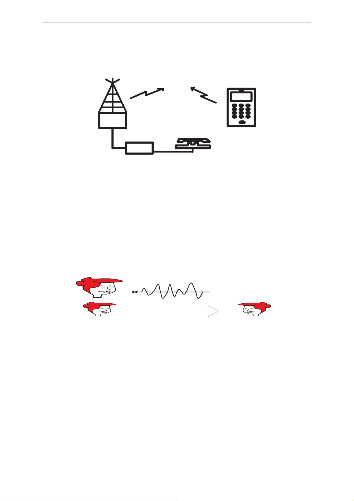
NHD–4 is a dual mode handportable Cellular phone product for the North
American dual mode CDMA/AMPS system.
The transceiver consist of four modules: UI–flex, RF/system module,
battery pack and mechanics.
NHD–4 offers analog and digital mode full rate speech services defined in
IS–96 and in analog mode provides six power levels at a maximum power
level of 0.6W ERP (450mW into 50 Ohm load) in power class III. The
transceiver has a retractable antenna and a connector for external
antenna and accessories. The user communicates with the phone via
LCD–display, keyboard and some audible tones.
The transceiver will support an Analog PCMCIA Card.
NHD–4 can be connected to different accessories such as chargers,
holders, hands–free units, data–adapters and handset through the bottom
system connector.
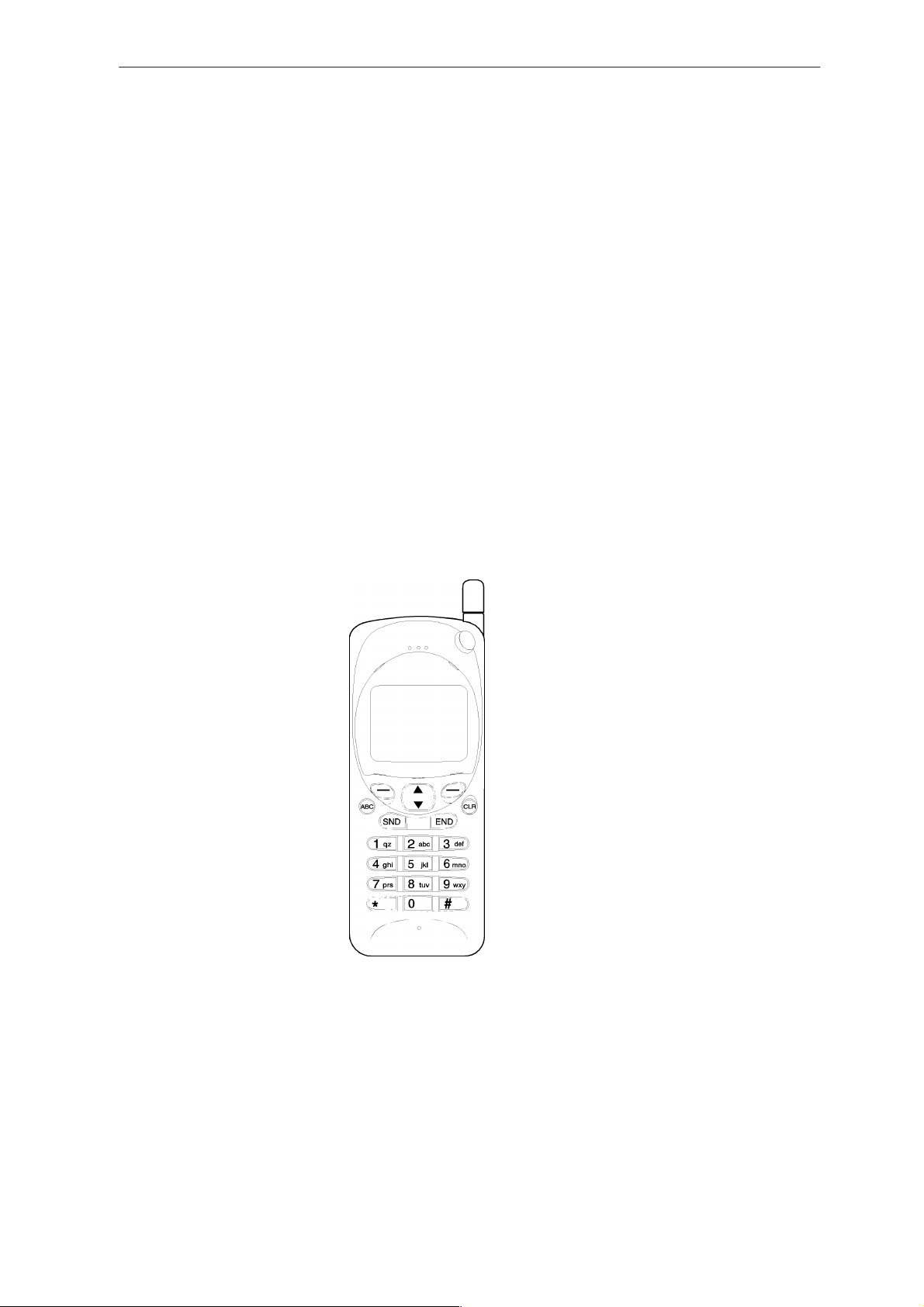
General Information
Original 11/97
NOKIA1
Figure 1. NHD–4
Page 2–3
Page 12
NHD–4
PAMS
General Information
Technical Documentation
List of Modules
Nokia1 NHD–4NX
Table 1. Nokia1 NHD–4NX 0500322
Name of module Type code Material
code
User interface DU8D 0200521 Nokia 1
System/RF GR1 0200519 CDMA 800 MHz Radio Module
Mechanics MNHD4NX 0260523 Nokia 1
Notes
Units and Accessories
Table 2. List of Transceivers
Name of Tranceiver Design Version Type Code Material Code
Transceiver CDMA 2180 Nokia 1 NHD–4NX 0500322
Table 3. List of Battery Packs
Design Type Technology Type Code Material
Code
Nokia1, CDMA Slim, 600 mAh NiMH BBH –1S 0670027
Nokia1, CDMA Std, 1100 mAh NiCd BBH–2H 0670030
Nokia1, CDMA Ext, 1700 mAh NiMH BBH –1H 0670028
Nokia1, CDMA Vibrator, 600 mAh NiMH BBT–1XV 0670119
Table 4. List of Chargers (
Name Type Code Material Code Notes
Fast Travel Charger ACH–4U 0675012 USA model
Cigarette Lighter Charger LCH–2 0675005 Universal
Desktop Charger CHH–2 0675022 Universal
HF Desktop Charger CHH–8 0675026 Universal
AC Adapter ACS–6U 0680018 USA model, needed for CHH–8
Page 2–4
Original 11/97
Page 13
PAMS
NHD–4
Technical Documentation
Table 5. List of Mobile Installation Accessories
Name Type Code Material Code Notes
Mobile Holder MBH–6 0620009
Mobile HF Charging Holder MCH–8 0620010
HF Junction Box HFJ–3 0694009
External HF Speaker HFS–6 0692005
HF Microphone HFM–4 0690002 Original
HF Microphone HFM–10 0690009 New , ”mouse” type
Power Cable PCH–4 0730009
External Audio Handset HSU–1 0640047
Compact HF PHF–1 0700017
Power Cable LCP–2 0680022
Mounting Plate MKE–1 0650007
Swivel Kit HHS–1 0650006 3 screws
Swivel Kit HHS–6 0650019 4 screws
General Information
Cable Holder CKH–1 0620016
Table 6. List of Data Accessories
Name Type Material code Notes
PC–Link Adapter DAU–2 0750029
Data Cable DKH–1 9780084 CHH–8 → PC Link
Data Cable DKH–2 0730041 Adapter Cable
Data Cable DKH–5 0730038 HP–PC Link
Table 7. List of General Accessories
Name Type code Material code Notes
Carry Strap SWH–1 0720005
Belt Clip BCH–2 0720022
Headset HFS–11 0690010 Over the head headset
Headset HDC–2 0694017 Button headset
Original 11/97
Page 2–5
Page 14

NHD–4
PAMS
General Information
Technical Documentation
Basic Specifications
Table 8. Basic Specifications
Parameter Notes
Cellular system CDMA/AMPS
TX frequency band 824.010...848.970 MHz
RX frequency band 869.010...893.970 MHz
Duplex spacing 45 MHz
Number of RF channels 832 Analog (see IS–95 6.1.1.1 for CDMA)
Channel spacing 30 kHz Analog (see IS–95 2.1.1.1 for CDMA)
Power Class III
Maximum output power 600 mW ERP (AMPS) 200 mW (CDMA)
Method of frequency synthesis Digital phase–locked loops
Frequency control VCTCXO
Receiver type IF, linear in D–mode, nonlinear in A–mode
Modulator type I/Q–baseband in D–mode, FM–modulator in A–mode
Operational Voltage 5.3V...8.8 V
Technical Specifications
Modes of Operation
NHD–4 operates in three modes:
1. In AMPS mode it operates in analog paging and voice channels.
2. In digital mode it operates on digital synch, paging pilot and traffic
channel.
3. Test mode (Local mode) used for troubleshooting and diagnostic
testing.
DC Characteristics
Table 9. Supply Voltages and Current Consumption
Line Symbol Minimum Typical /
Nominal
VBAT 5.3 6.0 8.8 V
Maxi-
mum
Unit / Notes
VCHAR 11.0 12.0 13.5 V / chargers
VCHAR 730 800 870 mA / chargers
Page 2–6
Original 11/97
Page 15
PAMS
NHD–4
Technical Documentation
AC Characteristics
Table 10. General RF Specifications
TX frequency band 824.04...848.970 MHz
RX frequency band 869.04...893.970 MHz
Duplex spacing 45 MHz
Number of RF channels 832 Analog
Channel spacing 30 kHz Analog
Analog Mode
Table 11. Transmitter Specifications for ANALOG mode
Modulation method FM
Deviation, speech and ST ±12 kHz peak
General Information
Deviation, WBD ±8 kHz peak
Deviation, SAT ±2 kHz peak
Deviation, voice and SAT ±14 kHz peak
Compressor 2:1
Output RF power (ERP from int. ant.) 26.3...6.3 dBm
Output RF power (ERP from int. ant.) 26.8...6.8 dBm
Number of power levels (2–7) 6
Carrier on/off switching time < 2ms
Frequency stability ±2.5 ppm
Harmonic and spurious emissions 43 +10*log (Po W) dB below carrier
Table 12 Receiver Specifications, for ANALOG mode
Sensitivity, 12 dB SINAD (C) –116 dBm
Hum and noise 32 dB
RSSI dynamic range 60 dB
Adjacent channel selectivity 16 dB
Alternate channel selectivity 60 dB
IMD attenuation, close spaced 65 dB
IMD attenuation, wide spaced 70 dB
Original 11/97
Page 2–7
Page 16
NHD–4
PAMS
General Information
Technical Documentation
Digital Mode
Table 13. Transmitter Specifications for CDMA mode
Spurious emissions in transmit
band
Spurious emissions out off transmit
band
TX noise floor at minimum TX pow-er–54 dBm/1.23 MHz (TX gate on), –60 dBm/1.23 MHz (TX
TX noise floor with TX disabled –61 dBm/MHz for all frequencies between 824 and 849 MHz
TX noise floor at RX band with
Max. output power
TX power control method Output_power (dBm) = –73 dBm – Receive_power (dBm) +
TX power initial accuracy +/–9 dB within value as specified by TX control method
–42 dBc in a 30 KHz BW for offsets > 885 KHz from center F
–54 dBc in a 30 KHz BW for offsets > 1.98 MHz from center
F
or –60 dBm/30 KHz and –54 dBm/1.23 MHz for offsets >
885 KHz from center Frequency
FCC rules
gate off)
–173 dBm/Hz (TBD) at RX input port
TX offset (dB). Open + closed loop AGC.
TX duty cycle 1/1, 1/2, 1/4, 1/8 variable rate with random slots. A slot is
1.25 ms. Rate is controlled by voice activity
TX offset control method From base station with one increments or decrement every
1.25 ms (but only during active transmit slot)
TX offset control step size 1 dB +/–0.5, and +/–20% over 10 steps in same direction
TX offset range +/–32 dB (+/–24 dB step range, +/–8 dB preset offset)
Modulator type I/Q modulator, OQPSK format
Peak to rms after modulation 6 dB
I/Q Modulator phase error +/–6 deg (+/– 4 deg for D/A and filter)
I/Q Modulator gain balance +/–0.65 dB (+/–0.35dB for D/A and filter)
I/Q Modulator input level 1Vpp
Table 14 Receiver RF specification, CDMA mode
Characteristics Min Typ Max Unit
Single tone desensitization,
+/–900KHz (Note 1)
Intermodulation spurious response level
Passband amplitude response
1 kHz
615 kHz
900 kHz
>900 kHz
Passband phase error
(mean2) response
Receiver gain –12 91 dB
–30 dBm
–30 dBm
–3 dB
–5
–73
–73
0.03 rad
dB
dB
dB
2
Receiver gain tolerance range
(without gain setting)
Page 2–8
14.8 dB
Original 11/97
Page 17
PAMS
NHD–4
Technical Documentation
Table 14 Receiver RF specification, CDMA mode (continued)
AGC range 96 dB
AGC accuracy (output level
variation for inputs –105 to
–25 dBm)
Baseband output level,
centered on Vref 1.45V
Baseband output level variation over RX input level of
–105 to –25 dBm
I/Q Amplitude imbalance –0.75 0.75 dB
I/Q Phase imbalance –7.5 +7.5 deg
–.5 +.5 dB
1 Vpp
–0.5 0.5 dB
General Information
UnitMaxTypMinCharacteristics
Mechanical Characteristics
Metric Units
Table 15. Mechanical Characteristics in Metric Units
Unit Dimensions
(mm)
(W x H x D)
Transceiver with standard
battery pack
Transceiver with standard
battery pack
Transceiver without battery
pack
Transceiver without battery
pack
Radio module 143x50x7 48 Common
UIF module 141x50x4 22
Mechanics 62 ...
Battery pack 600 mAh 56x101x8 104 42 NiMH, standard battery
Battery pack 1100 mAh 56x101x20 162 90 NiCd
Battery pack 1700 mAh 56x101x20 188 90 NiMH
56x148x25 238 179 Nokia 1
56x148x25 241 179 US CDMA
56x148x25 134 137 Nokia 1
56x148x25 137 137 US CDMA
Weight
(g)
67
Volume
(cm3)
Notes
depends on design version
Battery pack vibra NiMH
Original 11/97
Page 2–9
Page 18
NHD–4
PAMS
General Information
Technical Documentation
English Units
Table 16. Mechanical Characteristics in English Units
Unit Dimensions
(in.) (W x H x
D)
Transceiver with standard
battery pack
Transceiver with standard
battery pack
Transceiver without battery
pack
Transceiver without battery
pack
Radio module 5.6x2.0x0.28
UIF module 5.6x2.0x0.16
Mechanics 2.19 ...
Battery pack 600 mAh 2.2x4.0x0.31
Battery pack 1100 mAh 2.2x4.0x0.31
Battery pack 1700 mAh 2.2x4.0x0.31
Battery pack vibra NiMH
2.2x5.8x0.98
2.2x5.8x0.98 8.50 10.9 US CDMA
2.2x5.8x0.98
2.2x5.8x0.98 4.83 8.36 US CDMA
Weight
(oz.)
8.39
1.69
0.76
2.36
3.67
5.71
6.63
Volume
(in-
3
)
ches
10.9 Nokia 1
Nokia 1
8.36
Common
depends on design version
2.56
5.49
5.49
NiMH, standard battery
NiCd
NiMH
Notes
Page 2–10
Original 11/97
Page 19

Programme’s After Market Services
NHD–4 Series Transceivers
Chapter 3
System Overview
Original 11/97
Page 20

NHD–4
System Overview
Technical Documentation
CONTENTS
Acronyms 3–4. . . . . . . . . . . . . . . . . . . . . . . . . . . . . . . . . . . . . . . . . . . . . . . . . . . . . . .
Cellular History 3–5. . . . . . . . . . . . . . . . . . . . . . . . . . . . . . . . . . . . . . . . . . . . . . . . . .
AMPS Cellular Theory 3–6. . . . . . . . . . . . . . . . . . . . . . . . . . . . . . . . . . . . . . . . . . . .
Code Division Multiple Access (CDMA) 3–17. . . . . . . . . . . . . . . . . . . . . . . . . .
Quadrature Phase Shift Keying – QPSK 3–20. . . . . . . . . . . . . . . . . . . . . . .
The CDMA Signal 3–22. . . . . . . . . . . . . . . . . . . . . . . . . . . . . . . . . . . . . . . . . .
Processing Gain 3–22. . . . . . . . . . . . . . . . . . . . . . . . . . . . . . . . . . . . . . . . . . .
The CDMA Forward Link 3–24. . . . . . . . . . . . . . . . . . . . . . . . . . . . . . . . . . . .
V ocoder 3–25. . . . . . . . . . . . . . . . . . . . . . . . . . . . . . . . . . . . . . . . . . . . . . . . . . .
Convolutional Encoder 3–25. . . . . . . . . . . . . . . . . . . . . . . . . . . . . . . . . . . . . .
PAMS
Page No
Interleaver 3–26. . . . . . . . . . . . . . . . . . . . . . . . . . . . . . . . . . . . . . . . . . . . . . . . .
PN Code Generation 3–26. . . . . . . . . . . . . . . . . . . . . . . . . . . . . . . . . . . . . . .
Long Code Scrambling 3–28. . . . . . . . . . . . . . . . . . . . . . . . . . . . . . . . . . . . . .
Walsh Code User Channelization 3–28. . . . . . . . . . . . . . . . . . . . . . . . . . . . .
Walsh Codes 3–29. . . . . . . . . . . . . . . . . . . . . . . . . . . . . . . . . . . . . . . . . . . . . .
Orthogonal Functions 3–31. . . . . . . . . . . . . . . . . . . . . . . . . . . . . . . . . . . . . . .
Short Code Spreading 3–37. . . . . . . . . . . . . . . . . . . . . . . . . . . . . . . . . . . . . .
Forward Link Channel Format 3–37. . . . . . . . . . . . . . . . . . . . . . . . . . . . . . . .
CDMA Reverse Link 3–40. . . . . . . . . . . . . . . . . . . . . . . . . . . . . . . . . . . . . . . . . . .
Data Burst Randomizer 3–40. . . . . . . . . . . . . . . . . . . . . . . . . . . . . . . . . . . . .
Reverse Link Error Protection 3–41. . . . . . . . . . . . . . . . . . . . . . . . . . . . . . . .
64–ary Modulation 3–41. . . . . . . . . . . . . . . . . . . . . . . . . . . . . . . . . . . . . . . . . .
Reverse Channel Long Code Spreading 3–41. . . . . . . . . . . . . . . . . . . . . . .
Reverse Channel Short Code Spreading 3–41. . . . . . . . . . . . . . . . . . . . . .
Mobile Phone Operation 3–42. . . . . . . . . . . . . . . . . . . . . . . . . . . . . . . . . . . . . . .
Pilot Channel 3–42. . . . . . . . . . . . . . . . . . . . . . . . . . . . . . . . . . . . . . . . . . . . . .
Sync Channel 3–43. . . . . . . . . . . . . . . . . . . . . . . . . . . . . . . . . . . . . . . . . . . . . .
Page 3–2
Paging Channel 3–43. . . . . . . . . . . . . . . . . . . . . . . . . . . . . . . . . . . . . . . . . . . .
CDMA Call Initiation 3–44. . . . . . . . . . . . . . . . . . . . . . . . . . . . . . . . . . . . . . . .
Reverse Link Open Loop Power Control 3–44. . . . . . . . . . . . . . . . . . . . . . .
CDMA Call 3–45. . . . . . . . . . . . . . . . . . . . . . . . . . . . . . . . . . . . . . . . . . . . . . . .
Reverse Link Closed Loop Power Control 3–45. . . . . . . . . . . . . . . . . . . . .
CDMA Variable Rate Speech Coder 3–45. . . . . . . . . . . . . . . . . . . . . . . . . .
Mobile Power Bursting 3–45. . . . . . . . . . . . . . . . . . . . . . . . . . . . . . . . . . . . . .
The Rake Receiver 3–46. . . . . . . . . . . . . . . . . . . . . . . . . . . . . . . . . . . . . . . . .
CDMA Hand–offs 3–47. . . . . . . . . . . . . . . . . . . . . . . . . . . . . . . . . . . . . . . . . .
Original 11/97
Page 21

PAMS
NHD–4
Technical Documentation
System Overview
List of Figures
Figure 1. AMPS: BS/MS/MTX 3–6. . . . . . . . . . . . . . . . . . . . . . . . . . . . . . . . . . . .
Figure 2. AMPS: Audio 3–6. . . . . . . . . . . . . . . . . . . . . . . . . . . . . . . . . . . . . . . . . .
Figure 3. AMPS: Voice/RF 3–7. . . . . . . . . . . . . . . . . . . . . . . . . . . . . . . . . . . . . . .
Figure 4. AMPSTX/RX: 3–7. . . . . . . . . . . . . . . . . . . . . . . . . . . . . . . . . . . . . . . . . .
Figure 5. FM Modulation 3–8. . . . . . . . . . . . . . . . . . . . . . . . . . . . . . . . . . . . . . . . .
Figure 6. AMPS: Specifications 3–8. . . . . . . . . . . . . . . . . . . . . . . . . . . . . . . . . . .
Figure 7. AMPS: Cellular Frequencies 3–9. . . . . . . . . . . . . . . . . . . . . . . . . . . . .
Figure 8. AMP: Ch # & usage 3–9. . . . . . . . . . . . . . . . . . . . . . . . . . . . . . . . . . . . .
Figure 9. AMPS: Modulating signals 3–10. . . . . . . . . . . . . . . . . . . . . . . . . . . . . . .
Figure 10. AMPS: BS & Cell Set–up 3–11. . . . . . . . . . . . . . . . . . . . . . . . . . . . . . .
Figure 11. AMPS TX/RX registration 3–11. . . . . . . . . . . . . . . . . . . . . . . . . . . . . . .
Figure 12. AMPS: Call 3–13. . . . . . . . . . . . . . . . . . . . . . . . . . . . . . . . . . . . . . . . . . .
Figure 13. AMPS: Ch reuse & SAT Freq 3–14. . . . . . . . . . . . . . . . . . . . . . . . . . .
Figure 14. AMPS: Hand off 3–14. . . . . . . . . . . . . . . . . . . . . . . . . . . . . . . . . . . . . . .
Figure 15. AMPS: Mode Block Diagram 3–15. . . . . . . . . . . . . . . . . . . . . . . . . . . .
Figure 16. AMPS: TDMA & CDMA Freq and time domain 3–17. . . . . . . . . . . .
Figure 17. CDMA Capacity gains 3–18. . . . . . . . . . . . . . . . . . . . . . . . . . . . . . . . .
Figure 18. Analog, TDMA & CDMA Structure 3–19. . . . . . . . . . . . . . . . . . . . . . .
Figure 19. BPSK Modulator 3–20. . . . . . . . . . . . . . . . . . . . . . . . . . . . . . . . . . . . . .
Figure 20. I/Q Modulator 3–21. . . . . . . . . . . . . . . . . . . . . . . . . . . . . . . . . . . . . . . . .
Figure 21. CDMA Waveforms 3–22. . . . . . . . . . . . . . . . . . . . . . . . . . . . . . . . . . . .
Figure 22. CDMA Forward Link 3–24. . . . . . . . . . . . . . . . . . . . . . . . . . . . . . . . . . .
Figure 23. Convolutional encoder 3–25. . . . . . . . . . . . . . . . . . . . . . . . . . . . . . . . .
Figure 24. Interleaver 3–26. . . . . . . . . . . . . . . . . . . . . . . . . . . . . . . . . . . . . . . . . . . .
Figure 25. PN Code generator 3–26. . . . . . . . . . . . . . . . . . . . . . . . . . . . . . . . . . . .
Figure 26. PN Code generator w/mask ckt. 3–27. . . . . . . . . . . . . . . . . . . . . . . . .
Figure 27. Mask offset example 3–28. . . . . . . . . . . . . . . . . . . . . . . . . . . . . . . . . .
Figure 28. CDMA Forward Link 3–28. . . . . . . . . . . . . . . . . . . . . . . . . . . . . . . . . .
Figure 29. Walsh code example 3–29. . . . . . . . . . . . . . . . . . . . . . . . . . . . . . . . . .
Figure 30. Orthogonal Functions. 3–31. . . . . . . . . . . . . . . . . . . . . . . . . . . . . . . . .
Figure 31. Walsh Encoding Example 3–32. . . . . . . . . . . . . . . . . . . . . . . . . . . . . .
Figure 32. Walsh Decoding Example 3–33. . . . . . . . . . . . . . . . . . . . . . . . . . . . . .
Figure 33. Definition of orthonogonality 3–34. . . . . . . . . . . . . . . . . . . . . . . . . . . .
Figure 34. Forward Link Channel Format 3–39. . . . . . . . . . . . . . . . . . . . . . . . . .
Figure 35. CDMA Reverse Link 3–40. . . . . . . . . . . . . . . . . . . . . . . . . . . . . . . . . . .
Figure 36. CDMA Pilot & Synch Channel Timing 3–42. . . . . . . . . . . . . . . . . . . .
Figure 37. Mobile Power Bursting 3–46. . . . . . . . . . . . . . . . . . . . . . . . . . . . . . . . .
Figure 38. CDMA Hand–off 3–47. . . . . . . . . . . . . . . . . . . . . . . . . . . . . . . . . . . . . .
Page No
Original 11/97
Page 3–3
Page 22
NHD–4
Á
Á
Á
Á
Á
Á
Á
Á
Á
Á
Á
Á
Á
Á
Á
Á
System Overview
Acronyms
PAMS
Technical Documentation
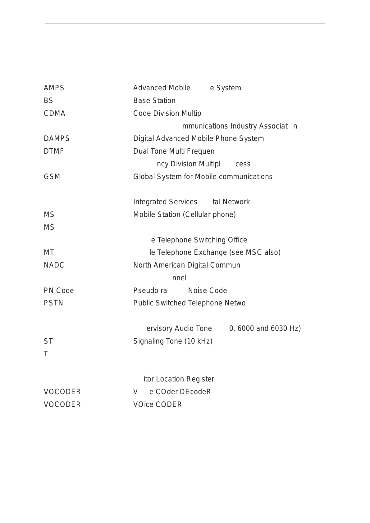
AMPS
BS
ББББББББ
CDMA
CTIA
DAMPS
ББББББББ
DTMF
FDMA
GSM
ББББББББ
HLR
ISDN
MS
ББББББББ
MSC
MTSO
MTX
ББББББББ
NADC
Advanced Mobile Phone System
Base Station
БББББББББББББББББББББ
Code Division Multiple Access
Cellular Telecommunications Industry Association
Digital Advanced Mobile Phone System
БББББББББББББББББББББ
Dual Tone Multi Frequency
Frequency Division Multiple Access
Global System for Mobile communications
БББББББББББББББББББББ
Home Location Register
Integrated Services Digital Network
Mobile Station (Cellular phone)
БББББББББББББББББББББ
Mobile Switching Center (see MTX also)
Mobile Telephone Switching Office
Mobile Telephone Exchange (see MSC also)
БББББББББББББББББББББ
North American Digital Communications (IS–54 DAMPS)
PCH
PN Code
ББББББББ
PSTN
RF
SAT
ББББББББ
ST
TCH
TS
ББББББББ
VLR
VOCODER
VOCODER
Paging Channel
Pseudo random Noise Code
БББББББББББББББББББББ
Public Switched Telephone Network
Radio Frequency
Supervisory Audio Tone (5970, 6000 and 6030 Hz)
БББББББББББББББББББББ
Signaling Tone (10 kHz)
Traffic CHannel
Time Slot
БББББББББББББББББББББ
Visitor Location Register
VOice COder DEcodeR
VOice CODER
Page 3–4
Original 11/97
Page 23

PAMS
NHD–4
Technical Documentation
System Overview
Cellular History
Mobile Radios have been in use for approximately 70 years and the cellular concept
was conceived in the 1940s. Public cellular mobile radio was not introduced in the
US until 1983.
In the beginning of the twentieth century, mobile radios were limited to shipboard
use due to the high power requirements and bulky tube radio technology.
Automotive systems in the 1920s operated on 6 volt batteries with a limited storage
capacity.
One of the first useful means of automotive mobile radio occurred in 1928 by the
Detroit police department. Transmission was broadcast from a central location and
could only be received by the mobile police radios.
Introduction of the first two way mobile application was delayed until 1933. This
simplex AM (Amplitude Modulation) push to talk system was introduced by the
police department in Bayonne, New Jersey. The first FM (Frequency Modulation)
mobile transmission (two frequency simplex) was used by the Connecticut State
Police at Hartford in 1940.
The first step towards mobile radio connection with the land line telephone network
was established in St. Louis in 1946. It was called an “urban” system and only
supported three channels.
In 1976, New York City had only 12 radio channels that supported 545 subscribers
with a waiting list of 3700.
In the 1970s, available cellular spectrum was constrained to frequencies above 800
MHz due to equipment design limitations and poor radio propagation characteristics
at frequencies above 1–GHz, this resulted in the allocation of the 825–890 MHz
region.
In 1974, 40 MHz of spectrum was allocated for cellular service and in 1986, an
additional 10 MHz of spectrum was added to facilitate expansion. The present
frequency assignments for the US Cellular system mobile phone is
824.040–848.970 MHz transmit and 869.040–893.970 MHz receive These bands
have been frequency divided (FDMA) into 30 kHz channels. This results in a
maximum capacity of 832 channels. These channels were then divided into two
groups with 416 channels assigned to each system.
Original 11/97
Page 3–5
Page 24
NHD–4
System Overview
AMPS Cellular Theory
R. F. Communication
BS
MTX
AMPS_1
Figure 1. AMPS: BS/MS/MTX
PAMS
Technical Documentation
Phone
Land Line Comms
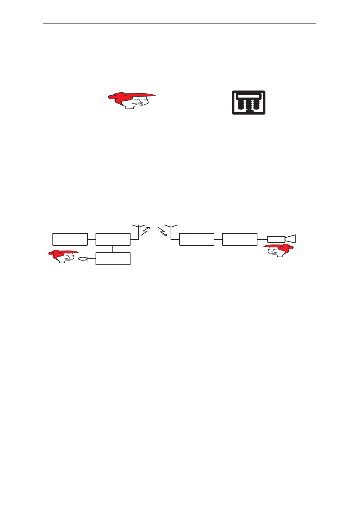
The main objective of a cellular system is to provide communications to many
mobile users. Communication between the Base Station and Mobile Phone is via a
Radio Frequency (RF) link. A Mobile Telephone Exchange (MTX) is the interface
between usually several base stations and Land line communications. The MTX
has a number of functions that include, controlling mobile phone transfers between
base stations, regulating mobile phone power output, establishing mobile phone
identity and billing for the air time.
300Hz–3000Hz
MIC
INFO
AMPS_2
Figure 2. AMPS: Audio
Audio signals
Cellular phones are designed to transmit audio signals in a frequency range of 300
Hz to 3000 Hz. This range of frequencies contains most of the intelligibility
necessary for one person to understand what another is saying. As the figure
above shows one person wants to talk to another who is some distance away.
Cellular phones allow communication between two or more people almost without
geographical restrictions.
Page 3–6
Original 11/97
Page 25
PAMS
NHD–4
Technical Documentation
System Overview
High frequency signals will radiate electromagnetic waves from an antenna.
Generally the higher the power the further the waves radiate. Our voice
information is at a low frequency, these frequencies will not radiate. The solution is
to put our information onto a high frequency carrier wave.
Phone
AMPS_3
Figure 3. AMPS: V oice/RF
These signals can then be radiated out an antenna and carry our information to the
receiver.
The function of placing information on a carrier wave is called MODULATION.
Carrier
Generation
800 MHz
Transmiter
Modulator
Audio
Amp
AMPS_4
RF
Amplifier
Receiver
Demodulator
Figure 4. AMPSTX/RX:
In AMPS mode information is placed on the carrier by changing the carrier’s
frequency. The modulating signal causes the carrier ’s frequency to increase and
decrease. This is called Frequency Modulation (FM), and changes to the carrier
frequency are known as deviation.
The receiver picks up RF signals, amplifies them and then retrieves (Demodulates)
information from the RF carrier. Demodulating changes in RF carrier frequency
recovers the original modulating audio frequencies.
Original 11/97
Page 3–7
Page 26
NHD–4
System Overview
PAMS
Technical Documentation
AMPS_5
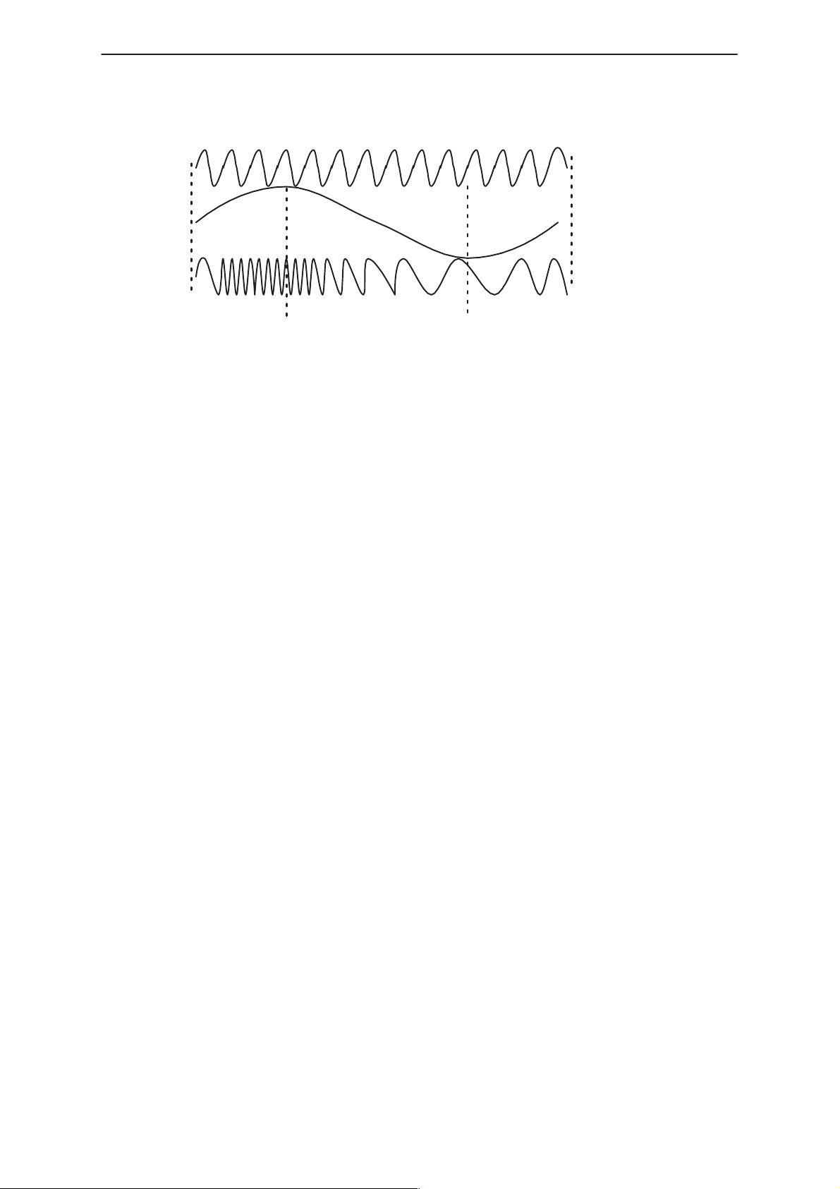
Frequency Modulation
+8 kHz
Unmodulated Carrier
1 kHz
Mod
Tone
–8kHz
Figure 5. FM Modulation
The figure above represents the effect of a 1 kHz audio modulating tone on an RF
carrier. The RF carrier in Figure 5 has a deviation of 8 kHz. A carrier deviation of
8 kHz means the frequency swings from plus 8 kHz to minus 8 kHz about the center
frequency.
When using Frequency Modulation (FM) how far from the center frequency the
carrier is deviated relates to how strong (loud) the modulating signal is. For
example if you whispered at the microphone the carrier might deviate only 1 or 2
kHz. On the other hand someone shouting at the microphone of their cellular
phone might cause it to deviate the maximum amount of 12 kHz. The standard
convention is that the positive part of the modulating signal will cause the carrier to
deviate to a higher frequency. While a negative modulation signal will cause the
carrier to go lower in frequency.
The rate, how fast the carrier frequency changes from high to low frequency, is
determined by the modulating signal’s frequency.
Advanced Mobile Phone System ––– AMPS
Full Duplex Operation
TX to RX Spacing = 45 MHz
Channel Width = 30 kHz
832 Channels total for the 800 MHz band
AMPS_6
Figure 6. AMPS: Specifications
The above information describes what AMPS stands for along with a “Nuts and
Bolts” description of the 800 MHz AMPS cellular system
Page 3–8
Original 11/97
Page 27
PAMS
NHD–4
Technical Documentation
AMPS_7
824.040MHz
Cellular Frequency Band
TX RX
RX
Phone
848.970MHz
Base Station
869.040MHz 893.970
TX
System Overview
MHz
Figure 7. AMPS: Cellular Frequencies
The 800 MHz cellular band consists of two 25 MHz wide frequency blocks. The
individual channel transmit and receive frequencies are spaced 45 MHz apart and
each channel is 30 kHz wide. Note that the transmit frequencies for a Base Station
are the receive frequencies for a cellular phone and vice–versa.
AMPS_7
824.040
Cellular Frequency Band
TX RX
Phone
848.970
869.040
893.970
MHz
RX
AMPS_8 A = A system provider channels
B = B system provider channels
MHz
Base Station
MHz
MHz
TX
Figure 8. AMP: Ch # & usage
The 800 MHz cellular phone band was divided into two parts by the FCC for
competitive reasons. When cellular phone service was first started channel
numbering was from 1 to 799. Later when the bottom 33 channels were added a
nonconsecutive channel numbering scheme was used. Cellular phones that were
in use when only 799 channels were available would have tuned to an incorrect
frequency if the channel numbering had been changed when the new channels were
added. Close examination will show that both “A” and “B” providers have an equal
number of channels.
When cellular phones were first introduced they scanned all available channels.
Present day cellular phone’s scan only the Control Channels. Most phones will
scan only the “A” or “B” control channels even though they are capable of scanning
all 42 channels. Air time is less expensive if only the phone’s Home channels are
used.
Original 11/97
Page 3–9
Page 28

NHD–4
System Overview
PAMS
Technical Documentation
Modulating Signals
SAT
5.97 kHz 6.0 kHz 6.03 kHz
To varify a constant RF
connection from BS & Phone
2 kHz
ST Signalling tone
10 kHz
Off–hook, On–hook
Hook Flash, Hand–off
8 kHz
Supervisory Audio Tone
Type:
Frequency:
Purpose:
Deviation:
Type:
Frequency:
Purpose:
Deviation:
AMPS_9
Data
(FSK) 10 kbps
Instructions & Information
between Base Station & Phone
8 kHz
V oice
300 Hz – 3 kHz
Person – Person
communication
12 kHz
Type:
Frequency:
Purpose:
Deviation:
Type:
Frequency:
Purpose:
Deviation:
Figure 9. AMPS: Modulating signals
As figure 9 illustrates an AMPS cellular phone can have four different types of
modulation.
DATA MODULATION
The first type of modulation a cellular phone uses when communicating with a Base
Station is Data. Data from the phone includes ESN, MIN, phone number to be
dialed and home system identification. Base Station data includes registration
conformation, notification of calls to the mobile, traffic channel assignment and
commands to adjust the mobile’s power output.
The data is Frequency Shift Keyed on the RF carrier. This is one way digital one’s
and zero’s can be modulated on an analog carrier. The 10 kHz data stream is
always transmitter by its self and not in combination with any other signal when in
the AMPS mode.
Supervisory Audio Tone (SAT)
SAT is used to insure that an RF link is being maintained between the mobile and
base station. The base station will transmit its assigned SAT frequency to the
mobile phone. When the mobile receives the SAT signal it will check to see that it is
the assigned frequency and then re–transmit SAT back to the base station. If either
the base station or the mobile fails to receive SAT the call will be terminated. SAT is
added to voice so a normal voice channel will have both voice and SAT. The user
does not hear SAT tones because they are filtered out with bandpass filters that only
allow voice frequencies to pass through.
Voice
Voice is transmitted in a range of frequencies of 300 Hz to 3 kHz. Remember that
SAT is also transmitted at the same time. The nominal deviation for Voice is 2.9
kHz and the maximum deviation for Voice is 12 kHz. Combining SAT and Voice
together will give a total maximum deviation of 14 kHz that the phone should never
exceed. If a mobile phone exceeds maximum deviation it will start interfering with
calls in adjacent channels.
Page 3–10
Original 11/97
Page 29
PAMS
NHD–4
Technical Documentation
System Overview
Signaling tone (ST)
Signaling tone is a plain 10 kHz tone. ST is used for signaling the base station
when the mobile phone is “off hook”, conversation is ended “on hook”, hook flash,
and handoff acknowledgment. When the mobile is being called,and is ringing, but
has not been taken “off hook” a continuous ST is transmitted to the base station.
When the mobile is taken “off hook”, answered, the ST is no longer sent. To
hang–up the “end” key is pressed, the mobile then sends out a 1.8 second burst of
ST. If during a conversation a mobile user wants “additional” service a
number/command is loaded into the mobile call memory and the “send” key is
pressed, the mobile will transmit ST for 400 ms. The base station responds will a
data acknowledgment, the mobile then sends its “additional” service request. When
a hand–off between base stations becomes necessary the MTX generates a
hand–off order and sends it to the mobile. The mobile stores this information and
sends a 50 ms burst of ST to the base station then changes to the new base station
and traffic channel. When the MTX detects SAT on the new channel the old base
station channel is shut down.
Base Station & Cell Set–up
X
Control Ch #
Traffic Ch #’s
Base Station
333
101 – 150
A4D7
ID
313
1 – 50
B9CE
320
201 – 250
8FB2
315
151 – 200
BC43
327
51 – 100
796F
Ch
333
313
329
327
330
315
322
AMPS_10
Info Rxd
A4D7
B9CE
–––––––
796F
–––––––
BC43
–––––––
Level
–100 dBm
–109 dBm
–120 dBm
–118 dBm
–120 dBm
–116 dBm
–120 dBm
Figure 10. AMPS: BS & Cell Set–up
When a cellular phone is first turned on it will scan the control channels. The phone
will record several different items of information, the channel number, Base Station
ID, System ID (SID) and the signal level of each Base Station received. In the
example Base Station A4D7 on control channel 333 was the strongest signal at a
level of –100 dBm. The mobile phone will then lock on control channel 333. Once
this is done the mobile phone is said to be “In Service”
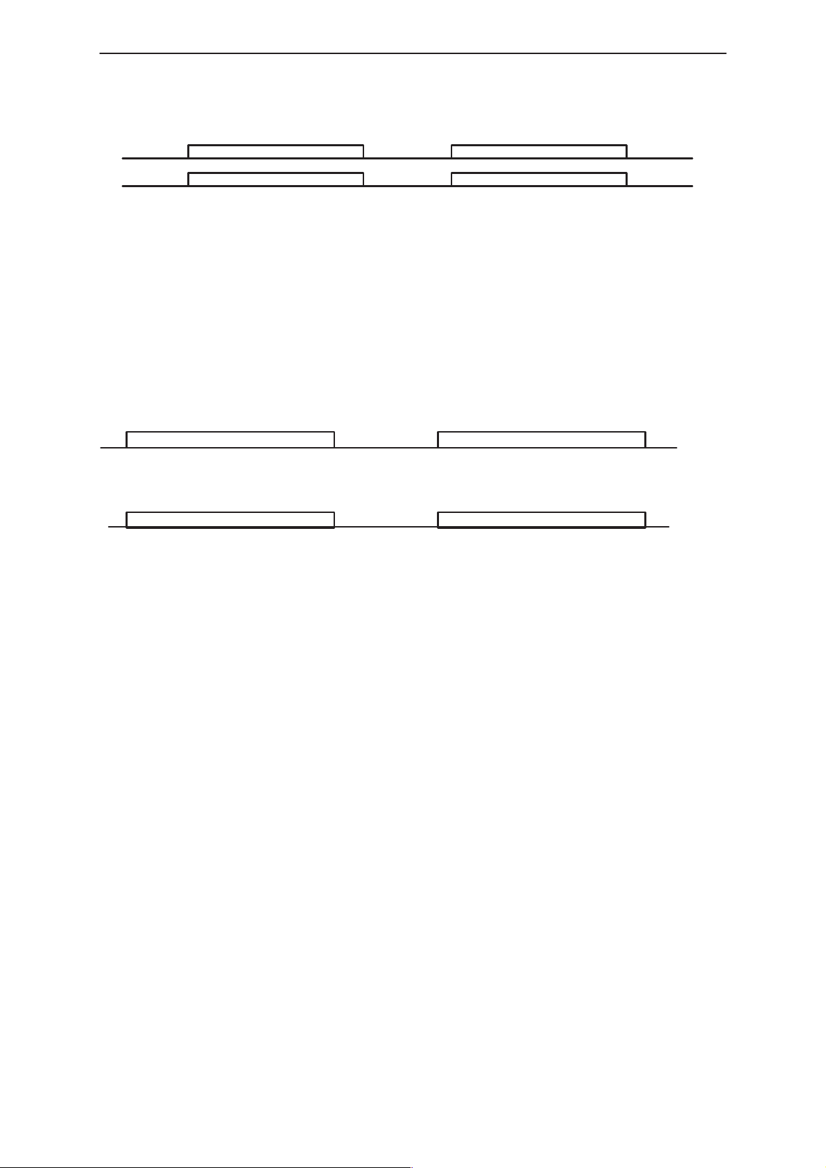
TX Registration
BS
1.
2. Data ESN/MIN
3.
4.
Figure 11. AMPS TX/RX registration
Channel 333
Data A4D7 ”Service”
Data ESN/MIN OK
Data A4D7
AMPS_11
Original 11/97
Page 3–11
Page 30

NHD–4
System Overview
Line 1 in figure 11 is the state the mobile phone was at in figure 10. The mobile has
found the strongest control channel and is “In service”.
In line 2 the mobile phone transmits it’s ESN/MIN to the Base Station (only if not in
its home area) using 10 kbytes/s data via the control channel.
Line 3 shows the Base Station sending the mobile phone a data transmission
confirming TX registration. At this time the Cellular Mobile Telephone Exchange
knows the mobile phone is ON and operating and which Base Station is currently in
contact with the mobile phone. This is important if the mobile phone gets a call
from another phone. The cellular system needs to know where each operating
mobile is in order to route calls to them.
Line 4 shows the Base Station back to continuously transmitting its ID. The mobile
phone stays on channel 333 and shows “In service”. Periodically the mobile will
rescan the control channels to make sure that it is still locked on the strongest
control channel.
Technical Documentation
PAMS
Page 3–12
Original 11/97
Page 31

PAMS
NHD–4
Technical Documentation
BS
1.
2. Data ESN/MIN/Dialed #
3.
4.
5. 1.8 sec (End Call) S.T.
CALL
Channel 333
Voice/SAT
AMPS_12
Data A4D7 ”Service”
Data ESN/MIN/OK
Goto 121/SAT=5970 Hz
System Overview
Figure 12. AMPS: Call
This is what happens when the mobile phone makes a “call”. As before the phone
is “In service” on control channel 333 with Base Station A4D7.
Line 2 shows the mobile phone sending a data stream to the Base Station that
contains the mobile’s ESN/MIN/phone # dialed.
In line 3 the Base Station confirms the mobiles data and instructs the mobile to go to
traffic channel 121 and to expect an SAT frequency of 5970 Hz.
In line 4 the Base Station and mobile are full duplex on traffic channel 121 with an
SAT frequency of 5970 Hz. Remember the SAT is used to confirm that a full duplex
(two way) link is operating between the Base Station and mobile phone.
Line 5 lists one of the four uses for Signaling Tone (ST). When the mobile phone
user finishes a call and presses “END” the phone sends out a 1.8 second burst of
ST that lets the Base Station know the call has ended. Another ST use is when the
mobile phone is being called. The phone sends a continuous ST signal back to the
Base Station until the mobile user answers the phone. As noted in the Modulating
Signals section the mobile also uses ST for “Hook Flash” and “Hand–off” signalling.
Original 11/97
Page 3–13
Page 32

NHD–4
System Overview
333
101–150
A4D7
5970 Hz
320
201–250
8FB2
AMPS_13
Channel Reuse and SAT Frequencies
Reused Voice Channels
313
1–50
B9CE
315
151–200
BC43
Control Ch #
Traffic Ch’s
Base Station
ID
327
51–100
796F
Technical Documentation
Different SAT freq
prevents hook–up
to other cell
319
101–150
B8C3
6030 Hz
PAMS
Figure 13. AMPS: Ch reuse & SAT Freq
In this example Base Stations A4D7 and B8C3 are using the same traffic channels.
Base Stations are normally spaced far enough apart so that two stations using the
same traffic channels will not interfere with each other. However!!! Under some
conditions it is possible for two stations like A4D7 and B8C3 to be received by one
mobile phone. The cure for this problem is different SAT frequencies. When a
mobile is ordered to a traffic channel it is given a traffic channel number and an SAT
frequency. If the mobile should be getting its traffic from A4D7 it expects to see an
SAT frequency of 5970 Hz. If an SAT frequency of 6030 were received, the mobile
would drop the call and try listening for the traffic channel that had 5970 Hz for SAT.
When an AMPS mobile station (MS) travels from one Base Station (BS) cell to
another a “Hand–off” must occur. As the mobile travels from “A” to “B” the signal
strength will decrease in “A” and increase in “B”. This information is sent from the
BS to the Mobile Telephone Exchange (MTX). Each BS has a receiver that can
scan all channels. When a hand–off is imminent the MTX instructs BS “B” to listen
for the MS about to be handed–off in order to insure that signal strength is
adequate. When the MTX decides its time for a hand–off, the traffic channel from
BS “A” to the mobile is interrupted and hand–off instructions are sent to the mobile.
The mobile then sends a 50 msec burst of Signalling Tone to confirm receipt of
instructions, then changes to the new Base Station, traffic channel and ST. The
user does not hear any data because the ear piece is muted when the phone is not
receiving SAT.
Handoff
D
AMPS_14
X
X
A
MTX
B
C
Page 3–14
Figure 14. AMPS: Hand off
Original 11/97
Page 33

PAMS
NHD–4
Technical Documentation
869–894
MHz
RX
Duplexer
TX
Power
Amplifier
& Driver
881.52
MHz
LNA
SAW Flter
BW 25 MHz
SAW
Filter
824–840
MHz
1st
Mixer
UHF VCO
914 – 939
MHz
Driver
Amps
45 MHz
IF
Amp
Analog
Modulation
VHF VCO
180 MHz
914–939 mhZ
SAW
Filter
824–840
MHz
2nd IF Amp & FM Det
Xtal
Filter
180 mhZ
TX Mix
455 kHz
2nd LO
44.545
MHz
2nd
IF Amp
TX gain
control
90 MHz
CDAGCT
Ceramic
Filter
455 kHz
2
System Overview
o
90
Ringing
Ckt
AMPS_15.DRW
FM
Det
Clipper
Amp
MIC
EAR
CODEC DSP CDSB CDRFI
To Analog Modulation
Figure 15. AMPS: Mode Block Diagram
The HD881 in AMPS mode is a dual conversion superheterodyne receiver. The
869.040 to 893.970 MHz receive band is passed through the receive side of the
duplex filter. The receive side of the duplexer bandpass filter is 25 MHz wide
centered at 881.52 MHz so that only cellular receive band frequencies will be
amplified by the LNA. After the LNA a second bandpass filter, a SAW (Surface
Acoustic Wave) filter is used to completely eliminate any frequencies outside the
receive band. The duplex and SAW filters also help eliminate any image
frequencies. Image frequencies are 45 MHz above the UHF VCO frequency. The
first mixer down converts the incoming signal by mixing the received frequency with
the UHF VCO, this produces a 45 MHz IF signal. A second mixer down converts
this 45 MHz IF to the second IF frequency of 455 kHz. The 455 kHz 2nd IF after
filtering is demodulated by the FM demodulator. Ten kbit/s data and SAT
(Supervisory Audio Tones) are separated in the CDRFI and these signals are sent to
the CDSB modem section where FSK data from the BS is demodulated. The RX
voice signal is converted to a digital bit stream in the CDRFI. Analog voice data is
sent to the AMPS Data Buffer in the CDSB. Analog voice data is sent from the
CDSB to the DSP for processing into a form that the Audio CODEC can use.
Analog voice data is converted to analog by the CODEC and then fed to the
earpiece.
Original 11/97
Page 3–15
Page 34

NHD–4
System Overview
An Audio Analyzer is used to determine the phones SINAD response. Minimum
receiver sensitivity is defined as the RF level (–116 dBm) that, when modulated in a
specified manner (8 kHz deviation with a 1 kHz tone) will result in a SINAD of at
least 12 dB. SINAD is an acronym for Signal, Noise and Distortion, not just the
signal to noise ratio.
The frequency scheme illustrated mixes the UHF VCO with the 90 MHz VHF VCO
and uses the difference frequency to arrive at the final transmit frequency. Transmit
voice is digitialized by the CODEC. This data is processed by the DSP then sent to
the CDSB for further processing. The analog data stream is converted to an analog
signal in the CDRFI. This analog data signal then frequency modulates the 180
MHz VHF VCO.
Technical Documentation
PAMS
Page 3–16
Original 11/97
Page 35

PAMS
NHD–4
Technical Documentation
Code Division Multiple Access (CDMA)
Amplitude
Amplitude Time
Time
RX Ch1 RX Ch...n TX Ch 1 TX Ch...n
Channelization – FDMA
Channelization – TDMA
3
2
1
3
2
1
Channelization – CDMA
Time
Forward Link B.S. M.S.
System Overview
Frequency
3
2
1
TX Ch...nTX Ch 1RX Ch...nRX Ch1
3
2
1
Frequency
Amplitude
PN Sequence
(short code)
PN Offset 1 PN Offset 2 PN Offset 512
. . .
Channelization – CDMA
Amplitude
Time
CDMA01.DRW
Reverse LinkM.S. B.S.
Allows Channalization
and privacy
42
2
possible
PN Sequence
(long code)
Figure 16. AMPS: TDMA & CDMA Freq and time domain
With FDMA Channelization (Analog AMPS), a channel is 30 kHz wide, this where all
the signal’s transmission power is concentrated. Different users are assigned
different frequency channels. FDMA is the acronym for Frequency Division Multiple
Access. Interference to and from adjacent channels is limited by the use of
bandpass filters that only pass signal’s within a specified narrow frequency band
while rejecting signals at other frequencies. The analog FM cellular system AMPS,
uses FDMA.
The US 800 MHz cellular system divides the allocated spectrum into 30 kHz
bandwidth channels. Narrowband FM modulation is used with AMPS, resulting in 1
call per 30 kHz of spectrum. Because of interference, the same frequency cannot
be used in every cell.
Original 11/97
Page 3–17
Page 36

NHD–4
System Overview
Technical Documentation
PAMS
The frequency reuse factor is a number representing how often the same frequency
can be reused. To provide acceptable call quality, a Carrier–to–Interference ratio
(C/I) of at least 18 dB is needed. Practical results show that in most cases to
maintain a 18 dB (C/I) a frequency reuse factor of 7 is required (see figure 18).
Please note that C/I is carrier to interference, not signal to noise ratio The resulting
capacity is one call per 210 kHz of spectrum in each cell.
With TDMA, a channel consists of a time slot in a periodic train of time intervals
making up a frame. A given signal’s energy is confined to one of these time slots.
The IS–54B TDMA standard provides a basic modulation efficiency of three voice
calls per 30 kHz of bandwidth. The resulting capacity is one call per 70 kHz of
spectrum or three times that of the analog FM system.
With CDMA (see Figure 16) each signal consists of a different pseudo random
binary sequence that modulates the carrier, spreading the spectrum of the
waveform. A large number of CDMA signals share the same frequency spectrum.
The signals are separated in the receivers by using a correlator that accepts only
signal energy from the selected binary sequence and de–spreads its spectrum
simultaneously. The other users’ signals, whose codes do not match, are not
de–spread and as a result, contribute only minimally to the noise and represent a
self–interference generated by the system. The forward link (B.S. to M.S.)
“channels” are separated by offsets in the short code PN sequence. Reverse link
channels are separated by different long code PN sequences. A detailed
description of the forward and reverse links is given later.
CDMA = 1.5 MHz 1 CDMA channel + 1.2288MHz
Capacity varies between 30 to 40 calls per CDMA
channel. Actual capacity depends Rho, processing
gain, error correction coding gain of M.S. vs signals
in cell and external cell signals.
AMPS = 1.5 MHz / 30kHz = 50 Channels
Capacity = 50 Channels / 7 (1 in 7 Frequency Reuse)
AMPS = 7 calls
DAMPS = 1.5 MHz / 30 kHz = 50 Channels
Capacity = 50 Channels / 7 x 3 Time Slots
DAMPS = 21 calls
GSM = 1.5 MHz / 200 kHz = 7 Channels
Capacity = 7 Channels / 7 x 8 Time Slots
GSM = 8 calls
Figure 17. CDMA Capacity gains
CDMA Capacity
Why should NOKIA go to so much trouble to develop CDMA? CAPACITY! To see
how CDMA increases capacity over present 800 MHz systems (AMPS and DAMPS)
lets look at a 1.5 MHz span of frequencies and compare. A CDMA frequency
channel is 1.2288 MHz wide however to provide guard bands in order to reduce
potential interference with adjacent analog channels a total of 1.5 MHz will be used.
Page 3–18
Original 11/97
Page 37

PAMS
NHD–4
Technical Documentation
System Overview
The AMPS, DAMPS, and GSM capacity examples in figure 17 assume that only one
channel out of every seven can be used. In a crowded metropolitan area, cellular
base stations are arranged like the top part of figure 18. Each base station is
surrounded by seven others so only one out every 7 channels can be used or
adjacent channel interference will occur. However, such is not the case for CDMA
because all users on a “CDMA Channel” operate on the same frequency. I’ve just
used the word “Channel” in a different way. Users in a given CDMA channel are
separated by different PN code sequences. According to information at the present
time there four designated CDMA frequency channels, so users on a given
frequency channel operate on the same frequency and are separated by different
PN code sequences which are also called “Channels”.
2
2
7
1
6
5
7
3
6
4
2
7
1
6
5
3
1
4
5
7
3
6
4
ANALOG & TDMA Cell Structure
Transmission range of
any given cell
2
3
1
4
5
CDMA Cell Structure
Transmission range of
any given celll
Figure 18. Analog, TDMA & CDMA Structure
1
1
1
1
1
1
1
1
1
1
1
1
1
1
1
1
1
1
1
1
1
1
1
1
1
1
1
1
CDMA03.DRW
Original 11/97
Page 3–19
Page 38

NHD–4
System Overview
Technical Documentation
PAMS
Quadrature Phase Shift Keying – QPSK
Forward link transmissions from the Base Station (BS) to the Mobile Subscriber
(MS) use QPSK modulation. QPSK is the sum of Two Binary Shift Keyed (BPSK)
signals. Figure 19 shows how a BPSK signal is made up.
Reference
carrier
input
Carrier
input
Carrier
input
DAMPS_4
A
T1 T2
B
++ ++
0 deg
–– ––
C
++
0 deg
––
Binary Phase Shift Keying
D1
D3
D4
D2
Binary input
D1 (on)
D3 and D4
(off)
D2 (on)
Binary 1
D1 (off)
D2 (off)
Binary 0
––
D3/D4
(on)
++
Modulator
output
Carrier
output
180 deg
Carrier
output
Binary
input
BPSK
output
Degrees
Radians
0 deg
10 1 10
0
TT
180
0
TT
TT
Binary input Output phase
Logic 0 180 deg
Logic 1 0 deg
180
Time
0
TT
TT
Figure 19. BPSK Modulator
Before starting any explanation about phase modulation a convention needs to be
established that will carry on throughout this study guide. Digital signals are
generally generated by use of a modulator that generates a sine and a cosine
channel and scales each channel by a factor that ranges from –1 to +1. What
the last sentence means is that the values of Data Channels are –1 and +1, not
0 and 1. A logic one will be “plus one” and a logic zero will be “minus one”.
In drawing ”B” of Figure 19, diodes D1 and D2 are forward biased into conduction
with a logic one. Transformer’s T1 and T2 are connected together in an in–phase
condition. In this case the output carrier’s signal would have the same phase as the
input.
In drawing “C” of Figure 19, diodes D3 and D4 are forwarded biased into conduction
with a logic zero. The output of T1 is cross connected to the input of T2 which will
result in the output being 180 degrees out of phase with the input signal.
Page 3–20
Original 11/97
Page 39

PAMS
NHD–4
Technical Documentation
SIN
CARRIER
INPUT
Values of Data Channels
are –1 and 1, not 0 and 1
90
Hybrid
COS
o
I DATA
Σ
CDMA04.DRW
Q DATA
For the reverse link
the Q data is delayed
by 1/2 clock chip. This
modulation is called
OQPSK (Offset Quadra
Phase Shift Keying)
System Overview
Figure 20. I/Q Modulator
In Figure 20 the 90 phase shifter is used to generate the sine and cosine channel
reference frequency. The two signal paths are called the “In phase” and the
“Quadrature phase” paths, therefore the name, I/Q modulator.
Original 11/97
Page 3–21
Page 40

NHD–4
System Overview
The CDMA Signal
PAMS
Technical Documentation
CDMA
Transmitter
Baseband
Data
9.6 kbps 19.2 kbps 1228.8 kbps
Background Noise
Encoding &
Interleaving
Walsh Code
Spreading
External Interference Other cell interference Other User Noise
CDMA
Receiver
1.25 MHz BW1.25 MHz BW
Walsh Code
Correlator
1228.8 kbps
Interference Sources
Figure 21. CDMA Waveforms
10 kHz BW10 kHz BW
Decode & De–
interleaving
19.2 kbps 9.6 kbps
Baseband
Data
CDMA05.DRW
To explain CDMA, some terms will have to be used that most persons are not
familiar with, but have patience they will be given a full explanation later in this Study
Guide. Forward link (BS to MS) CDMA starts with a narrowband signal that is
digitized speech. In this example the
full rate speech data rate
of 9600 bps is
shown.
Speech data rates from the VOCODER can vary from 1200 BPS to 9600 BPS when
using “Rate Set One” and 14.4, 7.2, 3.6, and 1.8 kbps when using “Rate Set Two”.
A specialized digital code called a Walsh Code provides “user” channelization for the
forward link (B.S to M.S.) and is used to encode the reverse link (B.S. to M.S.) user
data. The short code PN sequence
SPREADS
the baseband for both forward and
reverse links. The short code also provides channelization for BASE STATIONS on
the forward link by using a masking circuit. Masking will be explained later.
Processing Gain
One of the unique aspects of IS–95 standard CDMA is 21 dB of processing gain.
Processing gain is computed by using the formula 10 log(spread data rate) divided
by (Symbol rate). [10 log (1,228,800 / 19.2kBPS) = 21 dB]. If you calculate the
processing gain using the numbers in the last sentence the answer is 18 dB. The
extra 3 dB is comes from the same data being transmitted by the Q channel. If rate
set 2 is used the processing gain is 19.31 dB. When “your” CDMA signal is
transmitted all other CDMA signals along with background noise and any spurious
signals are considered interference.
Page 3–22
Original 11/97
Page 41

PAMS
NHD–4
Technical Documentation
When the wanted CDMA signal, “yours”, is received the correlation receiver
recovers “your” signal and rejects the rest. Looking at figure 21, the upper right
most part of the drawing shows what happens to the unwanted signals. The
unwanted signals are not de–spread so that each interfering signal only contributes
a little to the noise floor while “your” wanted signal is de–spread and will have an
acceptable signal–to–noise ratio. This is where the processing gain comes into
play. The processing gain is 21 dB and it takes a signal–to–noise ratio of about 7
dB for acceptable voice quality. This leaves 14 dB of processing gain to extract
“your” signal from the noise.
Here are some of the differences between CDMA and analog FM (AMPS).
Multiple users are on one frequency at the same time. RF engineers have spent a
lot of time and effort trying to keep signals on one channel so that adjacent channel
signals would not cause interference. CDMA technology places a great many
conversations (signals) on the same frequency.
In CDMA a channel is defined by various digital codes in addition to having different
frequencies. Analog FM channels are defined by different frequencies only.
System Overview
An analog FM (AMPS) cell site has a hard limit on the number of users it can
accommodate, only one call per frequency channel. CDMA has a soft capacity
limit. If cells surrounding a heavily loaded cell are lightly loaded then the heavily
loaded cell site can accommodate additional users. CDMA has a soft limit because
less “other cell” interference causes the total interference to be less. More calls can
also be accommodated at the expense of lower voice quality (S/N), this because
each additional user adds only a small amount of interference to the total.
Original 11/97
Page 3–23
Page 42

NHD–4
System Overview
The CDMA Forward Link
PAMS
Technical Documentation
20 MSEC
BLOCKS
Vocoded
Speech
data
Convolutional
Encoder
1/2
Rate
9.6
kbps
19.2
kbps
Long Code
Generator
CDMA Forward Link
Interleaver
19.2
kbps
Long Code
Decimator
1.2288
Mbps
1 of 64 bits
XOR
Power
Control
Bit
1 in 24
Decimator
MUX
800 Hz
Walsh Cover
XOR
1.2288
Mbps
Walsh Code
Generator
1.2288
Mbps
1.2288
Mbps
I Short Code
I Channel
Lo Pass
Filter
To I/Q
Modulator
Lo Pass
Filter
Q Channel
Q Short Code
CDMA06,DRW
Figure 22. CDMA Forward Link
When discussing the CDMA Forward Link, voice data will be shown at 9600 BPS
(full rate). Keep in mind that the Vocoded Speech rate can be 9600, 4800, 2400 or
1200 BPS when using Rate Set One. The Vocoded Speech rate is developed after
the CODEC in both the Base Station and the Mobile Phone.
Speech data is passed through a Convolutional Encoder that doubles the data rate.
This data is then Interleaved. Interleaving does not change the data rate but will
introduce some data time delay. The Long Code Generator running at 1.2288
Mbps develops the 242 bits long PN (Pseudo–random noise) code. The long code
Decimator uses one out of every 64 bits of the PN long code and exclusive OR’s this
decimated bit stream with the output of the Interleaver. At this point the data stream
is still running at 19.2 kbps. The 64 bit Walsh Code Generator output running at
1.2288 Mbps is exclusive OR’ed with the pervious exclusive OR gate’s output. The
baseband is now running at a data rate of 1.2288 Mbps, 64 times 19.2 kbps. The
Walsh encoded data stream is then split into I and Q channels, and then each
channel is spread with a short code. Then finally, signals are sent through a low
pass filter to the I/Q modulators.
Page 3–24
Original 11/97
Page 43

PAMS
NHD–4
Technical Documentation
System Overview
Vocoder
CDMA takes advantage of quiet times during speech to raise capacity. A variable
rate VOCODER is used; the vocoder’s output is at 9600 BPS when the user is
speaking. When the user pauses, or is listening, the data rate drops to 1200 BPS.
The data rates of 2400 and 4800 BPS are also used but not as often as the other
two. The data rate is based on speech activity and complexity. A decision is made
on the data rate every 20 msec. Normal speech has about a 40% activity factor. A
40% voice activity factor means that only 40% of transmission time is needed to
transmit the intelligible parts of speech.
Convolutional Encoder
Forward Error Protection
Data in
9600
pbs
D D D D
D D D D
Data Out
9600 bps
CDMA07.DRW
Data Out
9600 bps
Figure 23. Convolutional encoder
The forward CDMA link uses a half–rate convolutional encoder to provide error
correction capabilities. A half–rate encoder produces two output bits for every bit
input. This type of encoder accepts incoming serial data and outputs encoded data.
A convolutional encoder uses a shift register that contains a history of the bit
stream. It starts with all zeros and the data stream is shifted through. The two
9600 BPS output data streams are combined at a higher rate to provide a single
19,200 BPS data stream.
Original 11/97
Page 3–25
Page 44

NHD–4
System Overview
Technical Documentation
PAMS
Interleaver
Data In Data Out
12
34
5 Interleaver
12345
Figure 24. Interleaver
CDMA08.DRW
Interleaving is the process of shuffling the data before transmission with a
corresponding un–shuffle on the receiving end. The purpose is to spread the bit
errors. Bit errors tend to come in bursts due to fading, rather than uniformly spread
in time. Interleaving provides a more uniform bit error distribution so that one burst
of errors will not wipe out a whole digital word but only individual bits that can be
corrected by the convolutional decoding.
PN Code Generation
Pseudorandom Noise (PN)Sequences
00 1
10 0 0
Pattern = 1001011
01 0 0
Figure 25. PN Code generator
1
CDMA09.DRW
The illustration above is a highly simplified version of a PN code generator. It will
be left to the reader to fill in the blank registers. This generator will start repeating
after 7 bits. A CDMA long code register is 42 bits long and the short code register
15 bits long.
Page 3–26
Original 11/97
Page 45

PAMS
NHD–4
Technical Documentation
System Overview
The forward link Short Code is the same for all base stations. However a specific
mask is AND’ed with the output of the code generator to create a unique short code.
Even though the specific mask does not change the PN pattern the code is
considered unique relative to system time. This means that each specific mask will
shift the PN code to a unique delay with respect to system time and in this way the
shifted PN code is considered unique.
Here is another way of saying the same thing: PN codes used are required to have
low auto–correlation properties–––a time shifted version of itself correlated with itself
looks like random noise. Therefore a time shifted version is unique. Short Code
and Long Codes are handled the same: they use time shifted versions to be unique.
An example of a mask is shown in Figure 26. The three–bit shift register in figure
25 has a three–bit mask circuit connected to it in Figure 26.
11
0
11
1
0
11 1
11
11
0
0
0
0
00 1
11
00
1
0
0
0
0
10 0
11
00
1
0
11
0
0
1
1
1
0
0
0
1
11
11
Original 11/97
1
0
0
1
1
0
0
0
11
1
0
1
0
0
CDMA10.DRW
1
Figure 26. PN Code generator w/mask ckt.
Page 3–27
Page 46

NHD–4
Á
Á
ÁÁ
ÁÁ
ÁÁ
Á
Á
Á
Á
Á
Á
Á
Á
Á
Á
Á
Á
Á
Á
ÁÁ
ÁÁ
Á
ÁÁ
ÁÁ
Á
Á
Á
Á
Á
Á
Á
ÁÁ
ÁÁ
Á
ÁÁ
ÁÁ
Á
Á
Á
Á
Á
Á
Á
ÁÁ
System Overview
PAMS
Technical Documentation
Offset
ÁÁ
ÁÁ
01
10
11
ÁÁ
100
101
110
ÁÁ
1111
T0
1
0
1
0
1
0
1
T1
ÁÁ
ÁÁ
0
0
0
ÁÁ
1
1
1
ÁÁ
1
T2
Á
Á
0
1
1
Á
0
0
1
Á
1
T3
Á
Á
1
0
1
Á
1
0
1
Á
0
T4
Á
Á
0
1
1
Á
1
1
0
Á
0
T5
ÁÁ
ÁÁ
1
1
0
ÁÁ
1
0
0
ÁÁ
1
T6
Á
Á
1
1
0
Á
0
1
1
Á
0
Base
БББББ
Stations
БББББ
1
2
БББББ
3
4
5
БББББ
6
7
Figure 27. Mask offset example
The above example shows how different offsets will create different codes. Note
that none of the codes has been altered. Each one just starts at a different time.
Remember the CDMA system uses the same 15 bit linear feedback shift register to
generate the PN short code for both forward and reverse links. If figure 28 were
expanded to a 15–bit shift register the time shifted short codes for the 512 base
station channels would be shown.
Long Code Scrambling
In the forward link the long code is used to scramble voice data and provide some
measure of security. However the complete long code is not used, refer to Figure
28. A Long Code Decimator allows only one in every 64 bits of the Long Code to
be exclusively OR’ed with the Encoded Voice Data. This scrambling does not
increase the data rate because two 19.2 kbps data streams are being exclusive
OR’ed with each other.
Walsh Code User Channelization
The CDMA forward link figure will be repeated here to show where we are in the
CDMA forward link (base station to mobile) generation.
20 MSEC
BLOCKS
1.2288
Mbps
1.2288
Mbps
I Short Code
Lo Pass
Filter
Lo Pass
Filter
Q Short Code
CDMA06,DRW
I Channel
To I/Q
Modulator
Q Channel
Vocoded
Speech
data
Convolutional
Encoder
1/2
Rate
9.6
kbps
19.2
kbps
Long Code
Generator
Interleaver
1.2288
Mbps
XOR
19.2
kbps
Long Code
Decimator
1 of 64 bits
Power
Control
Bit
1 in 24
Decimator
MUX
800 Hz
Figure 28. CDMA Forward Link
Walsh Cover
XOR
1.2288
Mbps
Walsh Code
Generator
The 20 msec VOCODED speech data blocks have had an error correction routine
added in the Convolutional Encoder that increased the data rate to 19.2 ksps (kilo
symbols per second).
Page 3–28
Original 11/97
Page 47

PAMS
NHD–4
Technical Documentation
System Overview
The Interleaver changes the data order so only bits instead of whole words would be
lost because of data errors. The Long Code Generator generates a code that is
242 bits long. This code runs at 1.2288 Mbps and takes about 41.5 days before it
repeats. The PN (Pseudo–random) code is decimated by a factor of 64 that means
only one out of 64 bits is XOR’ed with the output of the Interleaver. The data rate at
this point is still 19.2 ksps because two 19.2 ksps data streams have been XOR’ed.
The 64 Walsh codes are used in the forward link as a means to uniquely identify
each user. The Walsh code generator runs at 1.2288 Mbps while the encoded
voice data runs at 19.2 kbps the ratio is 64 or 21 dB of processing gain. This
means that each data bit is XOR’ed with 64 Walsh code bits, one complete 64 bit
Walsh code. The voice data determines the polarity of the Walsh code. This
makes it easier for the CDMA mobile to find and decode its assigned Walsh code.
All base station’s use the same Walsh code 64 set. What gives each base station
its own unique identity will be explained in “Short Code Spreading”
The forward link is now running at its final rate of 1.2288 Mbps.
Walsh Codes
Walsh Codes in the CDMA forward link are used to “make” the CDMA forward
channels. Remember in analog phones a different frequency channel is used to
separate one cell phone user from another. TDMA cell phones use different time
slots to allow 3 phones to share one frequency channel. CDMA uses different
frequency channels like analog and TDMA cell phones. However, to separate
CDMA users on the same base station, different codes are used on the forward link
(Base Station to Mobile). IS–95 Standard CDMA uses Walsh code set 64. This
Walsh set has 64 unique codes each having 64 bits. Figure 29 shows how a Walsh
code set is built up.
W = 0
1
W =
2n
W W
W W
W =
W =
0 0
2
4
0 1
0 0 0 0
0 1 0 1
0 0 1 1
0 1 1 0
CDMA11.DRW
Figure 29. Walsh code example
Walsh code sets are generated by using the formula W2n = W W
W W .
In Walsh code set 2 it can be seen that the lower right digit is the logical not of the
other three digits. In Walsh code 4 the set 2 code is repeated three times with the
logical not being used in the lower right corner. The expansion number is always a
power of 2 and also notice that for each set the first code is always all zeros.
Original 11/97
Page 3–29
Page 48

NHD–4
System Overview
Walsh codes have the desirable characteristic of being “orthogonal” to each other.
What the heck does that mean(this is a rhetorical question)? ORTHOGONAL
Walsh Codes: when simultaneously transmitted they produce minimal interference
to other users. Look at the rows across in code set 4, any two rows have an equal
number of matches and mismatches. When correlation occurs between codes
(they match up) they will yield a cross correlation coefficient of 1. When the codes
do not match (correlate) the cross correlation coefficient is 0. Another way of
stating this is to say that when receiving the desired code a correlation receiver will
yield data and ignore all the unwanted codes.
Figure 30 overleaf should help sort out how Walsh orthogonal codes can keep
different CDMA users separated even though they are on the same frequency.
Technical Documentation
PAMS
Page 3–30
Original 11/97
Page 49

PAMS
NHD–4
Technical Documentation
System Overview
Orthogonal Functions
Two values are orthogonal if the result of exclusive–ORing them results in an equal
number of 1’s and 0’s.
Figure 30 uses the number 2 code, 0 1 0 1, in the Walsh code set 4 to “Orthogonally
Spread” some user input data. Each bit of user input data is exclusive–OR’ed with
the number 2 Walsh code that will result in TX Data shown in Figure 30.
Orthogonal Functions:
Two values are orthogonal if the result of
exclusive–or–ing them results in an equal
number of 1’s and 0’s
Orthogonal Spreading:
Note; Each Orthogonal Sequence in the
forward link will have 64 bits rather than
the 4 bits in this example.
User Input 1 0 0 1 1
Orthogonal
Sequence
TX Data
0 1 0 1 0 1 0 1 0 1 0 1 0 1 0 1 0 1 0 1
1 0 1 0 0 1 0 1 0 1 0 1 1 0 1 0 1 0 1 0
+1
–1
EXAMPLE: 1 1 1 1
0 1 0 1
1 0 1 0
Decoding using a Correct Orthogonal Function
RX Data 1 0 1 0 0 1 0 1 0 1 0 1 1 0 1 0 1 0 1 0
Correct
Function
Decoding with Incorrect Orthogonal Function
RX Data 0 1 0 1 0 1 0 1 0 1 0 1 0 1 0 1 0 1 0 1
Incorrect
Function
CDMA12.DRW
0 1 0 1 0 1 0 1 0 1 0 1 0 1 0 1 0 1 0 1
1 1 1 1 0 0 0 0 0 0 0 0 1 1 1 1 1 1 1 1
10 011
+1
–1
1 1 1 1 1 1 1 1 1 1 1 1 1 1 1 1 1 1 1 1
1 0 1 0 1 0 1 0 1 0 1 0 1 0 1 0 1 0 1 0
???? ?
+1
–1
Figure 30. Orthogonal Functions.
When the number 2 Walsh code is exclusive OR’ed with what is now the “RX data”
each number 2 Walsh code yields the original user input data 4 times. The IS–95
CDMA standard uses a 64–bit Walsh code so the mobile cell phone has the
transmitted data repeated 64 times. When the data is repeated 64 times, your have
processing gain. Repeating the processing gain information: 10 log 64 equals 18
dB: another 3 dB is added because the data is modulated on two channels, I and Q
for a total of 21 dB. This is one of the reasons why IS–95 CDMA is so tolerant of
noise. That is to say a signal–to–noise ratio that would render an analog signal
useless works fine with CDMA.
BUT JUST HOW DOES AN ORTHOGONAL WALSH CODE SEPARATE
DIFFERENT USERS?
At first it would seem that broadcasting 25 to 30 code streams on one frequency
would create an “electronic tower of babel”. To explain how Walsh encoding works
a Walsh code set 2 that has 2 orthogonal Walsh codes will be used in Figure 31.
Original 11/97
Page 3–31
Page 50

NHD–4
System Overview
PAMS
Technical Documentation
For a 1 input,
use Code 00
For a 0 input,
use Code 11
Channel A
Voice data
Channel A
Walsh Encoded
Voice Data
Walsh Encoding ExampleUser A
User A data 1011
+1
0
–1
+1
–1
+1
0
0
=
W
11
111
0
Sum of A & B
Walsh Encoded
Data Streams
0
11
0
2
0000
+2
+1
–1
–2
0 0 – User A
0 1 – User B
Channel B
Voice Data
Channel B
Walsh encoded
Voice data
+1
–1
+1
+1
–1
User B
User B data 0110
1
0
1
0
0110
0
1
00
CDMA13.DRW
For a 1 input
use code 01
For a 0 input
use code 10
111
00
Figure 31. Walsh Encoding Example
The example in Figure 31 uses Walsh Code set 2 that has two unique orthogonal
codes, “00” and “01”. Walsh code “00” will be assigned to User A and code “01” to
User B. Now in order for the Walsh code addition to work, bipolar values must be
used, so that a binary “0” has a value of “–1”. Also unless some higher math is
utilized one more convention must be used. If the voice data is a “0”, User A’s
Walsh code is “+1,+1”.
Page 3–32
Original 11/97
Page 51

PAMS
NHD–4
Technical Documentation
System Overview
Here is how the “bipolar” addition works:
Voice data 1 0 1 1
bipolar Walsh code –1–1 +1+1 –1–1 –1–1
Walsh encoded data 0 0 1 1 0 0 0 0
The voice data is added to both bipolar Walsh code numbers. The example is for
User A.
If the two Walsh encoded voice data channels are added together the result is a
data stream that varies between +2 and –2. Walsh code decoding will show that
both user data streams are contained in this waveform and further more they do not
interfere with each other.
Original User A Voice Data
+1
111
0
0
Original User B Voice Data
+1
0110
0
+2
+1
–1
–2
Multiply summed data with desired Walsh
code then find the area under the
resultant curve.
+2
+1
–1
–2
+1
X =
–1
00
+2
+1
–1
–2
Multiply summed data with desired Walsh
code then find the area under the
resultant curve.
+2
+1
=
–1
–2
CDMA14.DRW
+2
+1
1
–1
–2
Figure 32. Walsh Decoding Example
User A + B Walsh DataUser A + B Walsh Data
+2
+1
+1
X==
–1
–1
–2
–1
To see how user data is recovered from the summed signal lets extract the first bit of
each users’ data. First remember that each user bit is XOR’ed with two Walsh code
bits in this example. Taking the first two summed data bits, multiply them with
desired Walsh code. For User A this results in a wave form that starts at zero for
the first bit period and goes to +2 in the second bit period, 0 X –1 = 0 and –2 X –1 =
+2. The next step requires a little calculus, very little to figure “the area under the
curve”. Since the waveform is a square wave its not to hard. Add the two resultant
bits and divide by the number of bit periods, (0 + 2) / 2 = 1. User A’s first data bit is
“1”.
Original 11/97
Page 3–33
Page 52

NHD–4
W
Á
Á
Á
Á
Á
Á
Á
Á
Á
Á
Á
Á
Á
Á
Á
Á
Á
Á
Á
Á
Á
Á
Á
Á
Á
Á
Á
Á
Á
Á
Á
Á
Á
Á
Á
Á
Á
Á
Á
Á
Á
Á
Á
Á
Á
Á
Á
Á
Á
Á
Á
Á
Á
Á
Á
Á
Á
Á
Á
Á
Á
Á
Á
Á
Á
Á
Á
Á
Á
Á
Á
Á
Á
Á
Á
Á
Á
Á
Á
Á
Á
Á
Á
Á
Á
Á
Á
Á
Á
Á
Á
Á
Á
Á
Á
Á
Á
Á
Á
Á
Á
Á
Á
Á
Á
Á
Á
Á
Á
Á
Á
Á
Á
Á
Á
Á
Á
Á
Á
Á
Á
Á
Á
Á
Á
Á
Á
Á
Á
Á
Á
Á
Á
Á
Á
Á
Á
Á
Á
Á
Á
Á
Á
Á
Á
Á
Á
Á
Á
Á
Á
Á
Á
Á
Á
Á
Á
Á
Á
Á
Á
Á
Á
Á
Á
Á
Á
Á
Á
Á
Á
Á
Á
Á
Á
Á
Á
Á
Á
Á
Á
Á
Á
Á
Á
Á
Á
Á
Á
Á
Á
Á
Á
Á
Á
Á
Á
Á
Á
Á
Á
Á
Á
Á
Á
Á
Á
Á
Á
Á
Á
Á
Á
Á
Á
Á
System Overview
Technical Documentation
PAMS
To calculate User B’s first data bit multiply (0 X –1) and (–2 X 1) which equals zero,
minus two waveform. Find the area under the curve, (0 + (–2)) / 2 = –1, which is
User B’s first data bit.
It has been stated that Walsh codes are orthogonal and that this property results in
zero cross talk between Walsh code signals. Using bipolar numbers multiply Walsh
code “00” with Walsh code “01”. Add the resulting area and divide by the number of
bit periods and you will get zero. Figure 33 illustrates this.
+1
Walsh code
0 0
+1
Walsh code
0 1
+1
1
00
X=
0
CDMA15.DR
–1
–1
–1
Figure 33. Definition of orthonogonality
Another and simpler way to state that Walsh codes are orthogonal is that since the
codes have an equal number of matches and mismatches, they are orthogonal.
The full 64–bit by 64 code Walsh code set 64 has been reproduced in the following
table.
Walsh Code Set W64
0
00
00
00
00
00
00
00
00
00
00
00
00
00
00
00
00
01
01
00
110
110
00
Á
00
Á
01
Á
01
Á
00
Á
110
Á
110
Á
1
00
Á
2
01
Á
3
01
Á
00
Á
110
Á
110
Á
00
Á
01
Á
01
Á
00
Á
110
Á
110
00
01
01
00
110
110
Á
00
Á
01
Á
01
Á
00
Á
110
Á
110
Á
00
Á
01
Á
01
Á
00
Á
110
Á
110
Á
00
Á
01
Á
01
Á
00
Á
110
Á
110
00
01
01
00
110
110
Á
00
Á
01
Á
01
Á
00
Á
110
Á
110
Á
00
Á
01
Á
01
Á
00
Á
110
Á
110
Á
00
Á
01
Á
01
Á
00
Á
110
Á
110
00
01
01
00
110
110
Á
00
Á
01
Á
01
Á
00
Á
110
Á
110
Á
00
Á
01
Á
01
Á
00
Á
110
Á
110
Á
00
Á
01
Á
01
Á
00
Á
110
Á
110
4
00
111
Á
5
00
110
Á
6
01
10
Á
7
01
110
Á
00
01
Á
110
00
Á
110
1
8
00
00
Á
9
00
00
Á
1
01
01
Á
0
01
01
Á
1
00
00
1
110
110
Á
110
110
Á
Page 3–34
Á
Á
Á
Á
Á
Á
Á
Á
Á
Á
Á
Á
00
00
01
01
00
110
110
111
110
10
110
01
00
1
111
Á
110
Á
10
Á
110
Á
01
Á
00
Á
1
111
Á
110
Á
10
Á
110
Á
01
00
Á
1
Á
00
Á
00
Á
01
Á
01
Á
00
Á
110
Á
110
00
Á
00
Á
01
Á
01
Á
00
110
Á
110
Á
111
Á
110
Á
10
Á
110
Á
01
Á
00
Á
1
00
Á
00
Á
01
Á
01
Á
00
110
Á
110
Á
00
00
01
01
00
110
110
111
110
10
110
01
00
1
111
Á
110
Á
10
Á
110
Á
01
Á
00
Á
1
111
Á
110
Á
10
Á
110
Á
01
00
Á
1
Á
00
Á
00
Á
01
Á
01
Á
00
Á
110
Á
110
00
Á
00
Á
01
Á
01
Á
00
110
Á
110
Á
111
Á
110
Á
10
Á
110
Á
01
Á
00
Á
1
00
Á
00
Á
01
Á
01
Á
00
110
Á
110
Á
00
00
01
01
00
110
110
111
110
10
110
01
00
1
111
Á
110
Á
10
Á
110
Á
01
Á
00
Á
1
111
Á
110
Á
10
Á
110
Á
01
00
Á
1
Á
00
Á
00
Á
01
Á
01
Á
00
Á
110
Á
110
00
Á
00
Á
01
Á
01
Á
00
110
Á
110
Á
111
00
Á
110
Á
10
Á
110
Á
01
Á
00
Á
1
00
Á
00
Á
01
Á
01
Á
00
110
Á
110
Á
00
01
01
00
110
110
111
110
10
110
01
00
1
Á
Á
Á
Á
Á
Á
Á
Á
Á
Á
Á
Á
Original 11/97
111
110
10
110
01
00
1
111
110
10
110
01
00
1
Page 53

PAMS
Á
Á
Á
Á
Á
Á
Á
Á
Á
Á
Á
Á
Á
Á
Á
Á
Á
Á
Á
Á
Á
Á
Á
Á
Á
Á
Á
Á
Á
Á
Á
Á
Á
Á
Á
Á
Á
Á
Á
Á
Á
Á
Á
Á
Á
Á
Á
Á
Á
Á
Á
Á
Á
Á
Á
Á
Á
Á
Á
Á
Á
Á
Á
Á
Á
Á
Á
Á
Á
Á
Á
Á
Á
Á
Á
Á
Á
Á
Á
Á
Á
Á
Á
Á
Á
Á
Á
Á
Á
Á
Á
Á
Á
Á
Á
Á
Á
Á
Á
Á
Á
Á
Á
Á
Á
Á
Á
Á
Á
Á
Á
Á
Á
Á
Á
Á
Á
Á
Á
Á
Á
Á
Á
Á
Á
Á
Á
Á
Á
Á
Á
Á
Á
Á
Á
Á
Á
Á
Á
Á
Á
Á
Á
Á
Á
Á
Á
Á
Á
Á
Á
Á
Á
Á
Á
Á
Á
Á
Á
Á
Á
Á
Á
Á
Á
Á
Á
Á
Á
Á
Á
Á
Á
Á
Á
Á
Á
Á
Á
Á
Á
Á
Á
Á
Á
Á
Á
Á
Á
Á
Á
Á
Á
Á
Á
Á
Á
Á
Á
Á
Á
Á
Á
Á
Á
Á
Á
Á
Á
Á
Á
Á
Á
Á
Á
Á
Á
Á
Á
Á
Á
Á
Á
Á
Á
Á
Á
Á
Á
Á
Á
Á
Á
Á
Á
Á
Á
Á
Á
Á
Á
Á
Á
Á
Á
Á
Á
Á
Á
Á
Á
Á
Á
Á
Á
Á
Á
Á
Á
Á
Á
Á
Á
Á
Á
Á
Á
Á
Á
Á
Á
Á
Á
Á
Á
Á
Á
Á
Á
Á
Á
Á
Á
Á
Á
Á
Á
Á
Á
Á
Á
Á
Á
Á
Á
Á
Á
Á
Á
Á
Á
Á
Á
Á
Á
Á
Á
Á
Á
Á
Á
Á
Á
Á
Á
Á
Á
Á
Á
Á
Á
Á
Á
Á
Á
Á
Á
Á
Á
Á
Á
Á
Á
Á
Á
Á
Á
Á
Á
Á
Á
Á
Á
Á
Á
Á
Á
Á
Á
Á
Á
Á
Á
Á
Á
Á
Á
Á
Á
Á
Á
Á
Á
Á
Á
Á
Á
Á
Á
Á
Á
Á
Á
Á
Á
Á
Á
Á
Á
Á
Á
Á
Á
Á
Á
Á
Á
Á
Á
Á
Á
Á
Á
Á
Á
Á
Á
Á
Á
Á
Á
Á
Á
Á
Á
Á
Á
Á
NHD–4
Technical Documentation
1
00
111
111
Á
2
00
Á
1
01
Á
3
01
Á
1
00
Á
4
110
Á
1
110
5
Á
1
00
Á
6
00
Á
1
01
Á
7
01
1
00
Á
8
110
Á
1
110
Á
9
Á
2
00
0
00
Á
2
01
Á
1
01
Á
2
00
Á
2
110
Á
2
110
Á
3
Á
110
Á
10
Á
110
Á
01
Á
00
Á
1
Á
00
Á
00
Á
01
Á
01
00
Á
110
Á
110
Á
Á
111
110
Á
10
Á
110
Á
01
Á
00
Á
1
Á
110
10
110
01
00
1
00
00
01
01
00
110
110
00
00
01
01
00
110
110
00
Á
00
Á
01
Á
01
Á
00
Á
110
Á
110
Á
00
Á
00
Á
01
Á
01
00
Á
110
Á
110
Á
Á
111
110
Á
10
Á
110
Á
01
Á
00
Á
1
Á
00
Á
00
Á
01
Á
01
Á
00
Á
110
Á
110
Á
111
Á
110
Á
10
Á
110
01
Á
00
Á
1
Á
Á
111
110
Á
10
Á
110
Á
01
Á
00
Á
1
Á
111
Á
110
Á
10
Á
110
Á
01
Á
00
Á
1
Á
111
Á
110
Á
10
Á
110
01
Á
00
Á
1
Á
Á
00
00
Á
01
Á
01
Á
00
Á
110
Á
110
Á
111
110
10
110
01
00
1
111
110
10
110
01
00
1
111
110
10
110
01
00
1
00
Á
00
Á
01
Á
01
Á
00
Á
110
Á
110
Á
111
Á
110
Á
10
Á
110
01
Á
00
Á
1
Á
Á
00
00
Á
01
Á
01
Á
00
Á
110
Á
110
Á
00
Á
00
Á
01
Á
01
Á
00
Á
110
Á
110
Á
00
Á
00
Á
01
Á
01
00
Á
110
Á
110
Á
Á
00
00
Á
01
Á
01
Á
00
Á
110
Á
110
Á
111
Á
110
Á
10
Á
110
Á
01
Á
00
Á
1
Á
00
Á
00
Á
01
Á
01
00
Á
110
Á
110
Á
Á
111
110
Á
10
Á
110
Á
01
Á
00
Á
1
Á
111
110
10
110
01
00
1
00
00
01
01
00
110
110
00
00
01
01
00
110
110
00
Á
00
Á
01
Á
01
Á
00
Á
110
Á
110
Á
00
Á
00
Á
01
Á
01
00
Á
110
Á
110
Á
Á
111
110
Á
10
Á
110
Á
01
Á
00
Á
1
Á
System Overview
00
111
Á
00
Á
01
Á
01
Á
00
Á
110
Á
110
Á
111
Á
110
Á
10
Á
110
01
Á
00
Á
1
Á
Á
111
110
Á
10
Á
110
Á
01
Á
00
Á
1
Á
Á
110
Á
10
Á
110
Á
01
Á
00
Á
1
Á
111
Á
110
Á
10
Á
110
01
Á
00
Á
1
Á
Á
00
00
Á
01
Á
01
Á
00
Á
110
Á
110
Á
111
110
10
110
01
00
1
111
110
10
110
01
00
1
111
110
10
110
01
00
1
00
Á
00
Á
01
Á
01
Á
00
Á
110
Á
110
Á
111
Á
110
Á
10
Á
110
01
Á
00
Á
1
Á
Á
00
00
Á
01
Á
01
Á
00
Á
110
Á
110
Á
2
00
00
Á
4
00
Á
2
01
Á
5
01
Á
2
00
Á
6
110
Á
2
110
Á
7
2
00
Á
8
00
Á
2
01
Á
9
01
Á
3
00
Á
0
110
3
110
Á
1
Á
Á
00
Á
01
Á
01
Á
00
Á
110
Á
110
Á
111
Á
110
Á
10
Á
110
Á
01
Á
00
1
Á
Á
Original 11/97
111
110
10
110
01
00
1
111
110
10
110
01
00
1
111
Á
110
Á
10
Á
110
Á
01
Á
00
Á
1
Á
00
Á
00
Á
01
Á
01
Á
00
Á
110
110
Á
Á
111
Á
110
Á
10
Á
110
Á
01
Á
00
Á
1
Á
111
Á
110
Á
10
Á
110
Á
01
Á
00
1
Á
Á
111
Á
110
Á
10
Á
110
Á
01
Á
00
Á
1
Á
00
Á
00
Á
01
Á
01
Á
00
Á
110
110
Á
Á
00
00
01
01
00
110
110
00
00
01
01
00
110
110
00
Á
00
Á
01
Á
01
Á
00
Á
110
Á
110
Á
111
Á
110
Á
10
Á
110
Á
01
Á
00
1
Á
Á
00
Á
00
Á
01
Á
01
Á
00
Á
110
Á
110
Á
00
Á
00
Á
01
Á
01
Á
00
Á
110
110
Á
Á
00
Á
00
Á
01
Á
01
Á
00
Á
110
Á
110
Á
111
Á
110
Á
10
Á
110
Á
01
Á
00
1
Á
Á
111
110
10
110
01
00
1
111
110
10
110
01
00
1
111
Á
110
Á
10
Á
110
Á
01
Á
00
Á
1
Á
00
Á
00
Á
01
Á
01
Á
00
Á
110
110
Á
Á
111
Á
110
Á
10
Á
110
Á
01
Á
00
Á
1
Á
111
Á
110
Á
10
Á
110
Á
01
Á
00
1
Á
Á
111
00
Á
110
00
Á
10
01
Á
110
01
Á
01
00
Á
00
110
Á
1
110
Á
00
00
Á
00
00
Á
01
01
Á
01
01
Á
00
00
Á
110
110
110
110
Á
Á
Page 3–35
00
Á
00
Á
01
Á
01
Á
00
Á
110
Á
110
Á
111
Á
110
Á
10
Á
110
Á
01
Á
00
1
Á
Á
Page 54

NHD–4
Á
Á
Á
Á
Á
Á
Á
Á
Á
Á
Á
Á
Á
Á
Á
Á
Á
Á
Á
Á
Á
Á
Á
Á
Á
Á
Á
Á
Á
Á
Á
Á
Á
Á
Á
Á
Á
Á
Á
Á
Á
Á
Á
Á
Á
Á
Á
Á
Á
Á
Á
Á
Á
Á
Á
Á
Á
Á
Á
Á
Á
Á
Á
Á
Á
Á
Á
Á
Á
Á
Á
Á
Á
Á
Á
Á
Á
Á
Á
Á
Á
Á
Á
Á
Á
Á
Á
Á
Á
Á
Á
Á
Á
Á
Á
Á
Á
Á
Á
Á
Á
Á
Á
Á
Á
Á
Á
Á
Á
Á
Á
Á
Á
Á
Á
Á
Á
Á
Á
Á
Á
Á
Á
Á
Á
Á
Á
Á
Á
Á
Á
Á
Á
Á
Á
Á
Á
Á
Á
Á
Á
Á
Á
Á
Á
Á
Á
Á
Á
Á
Á
Á
Á
Á
Á
Á
Á
Á
Á
Á
Á
Á
Á
Á
Á
Á
Á
Á
Á
Á
Á
Á
Á
Á
Á
Á
Á
Á
Á
Á
Á
Á
Á
Á
Á
Á
Á
Á
Á
Á
Á
Á
Á
Á
Á
Á
Á
Á
Á
Á
Á
Á
Á
Á
Á
Á
Á
Á
Á
Á
Á
Á
Á
Á
Á
Á
Á
Á
Á
Á
Á
Á
Á
Á
Á
Á
Á
Á
Á
Á
Á
Á
Á
Á
Á
Á
Á
Á
Á
Á
Á
Á
Á
Á
Á
Á
Á
Á
Á
Á
Á
Á
Á
Á
Á
Á
Á
Á
Á
Á
Á
Á
Á
Á
Á
Á
Á
Á
Á
Á
Á
Á
Á
Á
Á
Á
Á
Á
Á
Á
Á
Á
Á
Á
Á
Á
Á
Á
Á
Á
Á
Á
Á
Á
Á
Á
Á
Á
Á
Á
Á
Á
Á
Á
Á
Á
Á
Á
Á
Á
Á
Á
Á
Á
Á
Á
Á
Á
Á
Á
Á
Á
Á
Á
Á
Á
Á
Á
Á
Á
Á
Á
Á
Á
Á
Á
Á
Á
Á
Á
Á
Á
Á
Á
Á
Á
Á
Á
Á
Á
Á
Á
Á
Á
Á
Á
Á
Á
Á
Á
Á
Á
Á
Á
Á
Á
Á
Á
Á
Á
Á
Á
Á
Á
Á
Á
Á
Á
Á
Á
Á
Á
Á
Á
Á
Á
Á
Á
Á
Á
Á
Á
Á
Á
Á
Á
Á
Á
Á
Á
Á
Á
Á
Á
Á
Á
Á
Á
System Overview
3
00
00
Á
2
00
Á
3
01
Á
3
01
Á
3
00
Á
4
110
Á
3
110
5
Á
3
00
Á
6
00
Á
3
01
Á
7
01
3
00
Á
8
110
Á
3
110
Á
9
Á
4
00
0
00
Á
4
01
Á
1
01
Á
4
00
Á
2
110
Á
4
110
Á
3
Á
00
Á
01
Á
01
Á
00
Á
110
Á
110
Á
111
Á
110
Á
10
Á
110
01
Á
00
Á
1
Á
Á
00
00
Á
01
Á
01
Á
00
Á
110
Á
110
Á
00
00
01
01
00
110
110
00
00
01
01
00
110
110
111
110
10
110
01
00
1
00
Á
00
Á
01
Á
01
Á
00
Á
110
Á
110
Á
111
Á
110
Á
10
Á
110
01
Á
00
Á
1
Á
Á
111
110
Á
10
Á
110
Á
01
Á
00
Á
1
Á
00
Á
00
Á
01
Á
01
Á
00
Á
110
Á
110
Á
00
Á
00
Á
01
Á
01
00
Á
110
Á
110
Á
Á
00
00
Á
01
Á
01
Á
00
Á
110
Á
110
Á
00
Á
00
Á
01
Á
01
Á
00
Á
110
Á
110
Á
111
Á
110
Á
10
Á
110
01
Á
00
Á
1
Á
Á
00
00
Á
01
Á
01
Á
00
Á
110
Á
110
Á
00
00
01
01
00
110
110
00
00
01
01
00
110
110
111
110
10
110
01
00
1
00
Á
00
Á
01
Á
01
Á
00
Á
110
Á
110
Á
111
Á
110
Á
10
Á
110
01
Á
00
Á
1
Á
Á
111
110
Á
10
Á
110
Á
01
Á
00
Á
1
Á
111
Á
110
Á
10
Á
110
Á
01
Á
00
Á
1
Á
111
Á
110
Á
10
Á
110
01
Á
00
Á
1
Á
Á
111
110
Á
10
Á
110
Á
01
Á
00
Á
1
Á
111
Á
110
Á
10
Á
110
Á
01
Á
00
Á
1
Á
00
Á
00
Á
01
Á
01
00
Á
110
Á
110
Á
Á
111
110
Á
10
Á
110
Á
01
Á
00
Á
1
Á
Technical Documentation
111
111
111
110
10
110
01
00
1
111
110
10
110
01
00
1
00
00
01
01
00
110
110
Á
110
Á
10
Á
110
Á
01
Á
00
Á
1
Á
00
Á
00
Á
01
Á
01
00
Á
110
Á
110
Á
Á
00
00
Á
01
Á
01
Á
00
Á
110
Á
110
Á
Á
110
Á
10
Á
110
Á
01
Á
00
Á
1
Á
111
Á
110
Á
10
Á
110
01
Á
00
Á
1
Á
Á
111
110
Á
10
Á
110
Á
01
Á
00
Á
1
Á
111
Á
110
Á
10
Á
110
Á
01
Á
00
Á
1
Á
00
Á
00
Á
01
Á
01
00
Á
110
Á
110
Á
Á
111
110
Á
10
Á
110
Á
01
Á
00
Á
1
Á
111
110
10
110
01
00
1
111
110
10
110
01
00
1
00
00
01
01
00
110
110
PAMS
111
Á
110
Á
10
Á
110
Á
01
Á
00
Á
1
Á
00
Á
00
Á
01
Á
01
00
Á
110
Á
110
Á
Á
00
00
Á
01
Á
01
Á
00
Á
110
Á
110
Á
4
00
111
Á
4
00
110
Á
4
01
10
Á
5
01
110
Á
4
00
01
Á
6
110
00
Á
4
110
1
Á
7
4
00
00
Á
8
00
00
Á
4
01
01
Á
9
01
01
Á
5
00
00
Á
0
110
110
5
110
110
Á
1
Á
Page 3–36
Á
Á
Á
Á
Á
Á
Á
Á
Á
Á
Á
Á
Á
Á
111
110
10
110
01
00
1
00
00
01
01
00
110
110
00
Á
00
Á
01
Á
01
Á
00
Á
110
Á
110
Á
00
Á
00
Á
01
Á
01
Á
00
Á
110
110
Á
Á
00
Á
00
Á
01
Á
01
Á
00
Á
110
Á
110
Á
111
Á
110
Á
10
Á
110
Á
01
Á
00
1
Á
Á
111
Á
110
Á
10
Á
110
Á
01
Á
00
Á
1
Á
111
Á
110
Á
10
Á
110
Á
01
Á
00
1
Á
Á
111
110
10
110
01
00
1
111
110
10
110
01
00
1
00
Á
00
Á
01
Á
01
Á
00
Á
110
Á
110
Á
111
Á
110
Á
10
Á
110
Á
01
Á
00
1
Á
Á
111
Á
110
Á
10
Á
110
Á
01
Á
00
Á
1
Á
111
Á
110
Á
10
Á
110
Á
01
Á
00
1
Á
Á
00
Á
00
Á
01
Á
01
Á
00
Á
110
Á
110
Á
111
Á
110
Á
10
Á
110
Á
01
Á
00
1
Á
Á
00
00
01
01
00
110
110
111
110
10
110
01
00
1
111
Á
110
Á
10
Á
110
Á
01
Á
00
Á
1
Á
111
Á
110
Á
10
Á
110
Á
01
Á
00
1
Á
Á
111
Á
110
Á
10
Á
110
Á
01
Á
00
Á
1
Á
00
Á
00
Á
01
Á
01
Á
00
Á
110
110
Á
Á
00
00
00
01
01
00
110
110
00
00
01
01
00
110
110
111
Á
110
Á
10
Á
110
Á
01
Á
00
Á
1
Á
00
Á
00
Á
01
Á
01
Á
00
Á
110
110
Á
Á
Á
00
Á
01
Á
01
Á
00
Á
110
Á
110
Á
00
Á
00
Á
01
Á
01
Á
00
Á
110
110
Á
Á
Original 11/97
Page 55

PAMS
Á
Á
Á
Á
Á
Á
Á
Á
Á
Á
Á
Á
Á
Á
Á
Á
Á
Á
Á
Á
Á
Á
Á
Á
Á
Á
Á
Á
Á
Á
Á
Á
Á
Á
Á
Á
Á
Á
Á
Á
Á
Á
Á
Á
Á
Á
Á
Á
Á
Á
Á
Á
Á
Á
Á
Á
Á
Á
Á
Á
Á
Á
Á
Á
Á
Á
Á
Á
Á
Á
Á
Á
Á
Á
Á
Á
Á
Á
Á
Á
Á
Á
Á
Á
Á
Á
Á
Á
Á
Á
Á
Á
Á
Á
Á
Á
Á
Á
Á
Á
Á
Á
Á
Á
Á
Á
Á
Á
Á
Á
Á
Á
Á
Á
Á
Á
Á
Á
Á
Á
Á
Á
Á
Á
Á
Á
Á
Á
Á
Á
Á
Á
Á
Á
Á
Á
Á
Á
Á
Á
Á
Á
Á
Á
Á
Á
Á
Á
Á
Á
Á
Á
Á
Á
Á
Á
Á
Á
Á
Á
Á
Á
Á
Á
Á
Á
Á
Á
Á
Á
Á
Á
Á
Á
Á
Á
Á
Á
Á
Á
Á
Á
Á
Á
Á
Á
Á
Á
Á
Á
Á
Á
Á
Á
Á
Á
Á
Á
Á
Á
Á
Á
Á
Á
Á
Á
Á
Á
Á
Á
Á
Á
Á
Á
Á
Á
Á
Á
Á
Á
Á
Á
Á
Á
Á
Á
Á
Á
Á
Á
Á
Á
Á
Á
Á
Á
Á
Á
Á
Á
NHD–4
Technical Documentation
5
00
111
00
Á
2
00
Á
5
01
Á
3
01
Á
5
00
Á
4
110
Á
5
110
5
Á
5
00
Á
6
00
Á
5
01
Á
7
01
5
00
Á
8
110
Á
5
110
Á
9
Á
6
00
0
00
Á
6
01
Á
1
01
Á
6
00
Á
2
110
Á
6
110
Á
3
Á
110
Á
10
Á
110
Á
01
Á
00
Á
1
Á
00
Á
00
Á
01
Á
01
00
Á
110
Á
110
Á
Á
111
110
Á
10
Á
110
Á
01
Á
00
Á
1
Á
00
01
01
00
110
110
111
110
10
110
01
00
1
111
110
10
110
01
00
1
111
Á
110
Á
10
Á
110
Á
01
Á
00
Á
1
Á
111
Á
110
Á
10
Á
110
01
Á
00
Á
1
Á
Á
00
00
Á
01
Á
01
Á
00
Á
110
Á
110
Á
111
Á
110
Á
10
Á
110
Á
01
Á
00
Á
1
Á
111
Á
110
Á
10
Á
110
01
Á
00
Á
1
Á
Á
111
110
Á
10
Á
110
Á
01
Á
00
Á
1
Á
00
Á
00
Á
01
Á
01
Á
00
Á
110
Á
110
Á
111
Á
110
Á
10
Á
110
01
Á
00
Á
1
Á
Á
00
00
Á
01
Á
01
Á
00
Á
110
Á
110
Á
111
110
10
110
01
00
1
00
00
01
01
00
110
110
00
00
01
01
00
110
110
00
Á
00
Á
01
Á
01
Á
00
Á
110
Á
110
Á
00
Á
00
Á
01
Á
01
00
Á
110
Á
110
Á
Á
111
110
Á
10
Á
110
Á
01
Á
00
Á
1
Á
111
Á
110
Á
10
Á
110
Á
01
Á
00
Á
1
Á
111
Á
110
Á
10
Á
110
01
Á
00
Á
1
Á
Á
111
110
Á
10
Á
110
Á
01
Á
00
Á
1
Á
00
Á
00
Á
01
Á
01
Á
00
Á
110
Á
110
Á
111
Á
110
Á
10
Á
110
01
Á
00
Á
1
Á
Á
00
00
Á
01
Á
01
Á
00
Á
110
Á
110
Á
111
110
10
110
01
00
1
00
00
01
01
00
110
110
00
00
01
01
00
110
110
00
Á
00
Á
01
Á
01
Á
00
Á
110
Á
110
Á
00
Á
00
Á
01
Á
01
00
Á
110
Á
110
Á
Á
111
110
Á
10
Á
110
Á
01
Á
00
Á
1
Á
System Overview
00
111
Á
00
Á
01
Á
01
Á
00
Á
110
Á
110
Á
00
Á
00
Á
01
Á
01
00
Á
110
Á
110
Á
Á
00
00
Á
01
Á
01
Á
00
Á
110
Á
110
Á
Á
110
Á
10
Á
110
Á
01
Á
00
Á
1
Á
00
Á
00
Á
01
Á
01
00
Á
110
Á
110
Á
Á
111
110
Á
10
Á
110
Á
01
Á
00
Á
1
Á
00
00
01
01
00
110
110
111
110
10
110
01
00
1
111
110
10
110
01
00
1
111
Á
110
Á
10
Á
110
Á
01
Á
00
Á
1
Á
111
Á
110
Á
10
Á
110
01
Á
00
Á
1
Á
Á
00
00
Á
01
Á
01
Á
00
Á
110
Á
110
Á
Short Code Spreading
The Forward Channel is spread one–more–time. The final spreading uses a Short
Code that is 215 (32,768) bits long, runs at 1.2288 Mbps and repeats every 26.667
msec. As previously stated all base stations use the same set of Walsh codes, a
short code combined with an “offset” mask allows each base station to have a
unique identification. These “PN Offsets” are separated by multiples of sixty–four
1.2288 Mbps clock chips which allows 512 unique time offsets for base station
identification (32768 bits / 64 bits = 512 offsets). By XOR’ing the Walsh encoded
channels with the offset short code, each base station can reuse all 64 Walsh codes
and be uniquely identified from other adjacent cells using the same CDMA
frequency channel.
Forward Link Channel Format
First of all remember the word “Channel” means a different “PN Code Sequence”
and not a different frequency for this part of the discussion.
A base station transmitter signal is a composite of at least 4 and as many as 42
different channels depending on interference and the Rho of the mobiles. Rho is a
figure of merit for specifying: percentage of transmitted power that correlates to the
ideal code.
Original 11/97
Page 3–37
Page 56

NHD–4
System Overview
The “Pilot Channel” can be compared with the control channels used in analog.
The “Pilot Channel” is unmodulated Walsh code zero spread with Short Code that
has a unique mask applied in order for mobiles to identify cells from each other.
Pilot channel power is the strongest channel from the base station, with about 20%
of the total output power. The Pilot Channel provides the mobile with an easy to
demodulate strong signal that is used as a time reference.
The “Sync Channel” transmits timing information and always uses Walsh code 32
which is half zero’s and half one’s. The most important timing information contains
the state of the long code feedback shift registers 320 milli–seconds in the future.
The mobile can load this information into its long code generator, and start the
generator at the proper time. Long code state information is not all that is sent by
the sync channel but is one of the more important data.
The “Paging Channel” is the forward links digital control channel. Quite a lot of
information is sent to the mobile on this channel, a more complete discussion of all
four channels will be given in the section on how a CDMA mobile operates. The
first paging channel is always Walsh code one. If more paging channels are
needed Walsh codes 2 through 7 can be used.
Technical Documentation
PAMS
The “Traffic Channel” is the same thing as an analog voice channel. This is where
conversations take place. At least 55 Walsh codes are available for use as traffic
channels but the actual number that can be used is around 30 at present.
When all the various channels have been Walsh modulated they are split into I and
Q channels which are re–spread with the short code to provide base station identity,
filtered to reduce bandwidth and converted to analog signals. The analog I and Q
signals from all the channels are summed together and sent to the I/Q modulator for
modulation onto an RF carrier.
Figure 34, “Forward Link Channel Format “shows how the various channels are
made up.
Page 3–38
Original 11/97
Page 57

PAMS
NHD–4
Technical Documentation
Pilot Channel: All 0’s
Sync Channel
Data
1200 bps
Paging Channel
Data
9.6 kbps
4.8 kbps
2.4 kbps
Forward Traffic
Channel Data
9.6 kbps
4.8 kbps
2.4 kbps
1.2 kbps
User Long
Code mask
Convolutional
Encoder
Convolutional
Encoder
Paging Channel
Long Code Mask
Convolutional
Encoder
Long Code
Generator
Interleaver
Interleaver
Long Code
Generator
Interleaver
Long Code
Decimator
1 in 64 bits
19.2
kbps
19.2
kbps
+
+
4800
bps
Power
Control
Bit
+
+
+
MUX
W0
W32
W 1 – 7
1.2288
MHz
1.2288
MHz
1.2288
MHz
W 8–31 &
W 33–63
+
System Overview
I Channel Short Code
Pilot PN Sequence
+
Summer
CDMA16.DRW
+
Q Channel Short Code
Pilot PN Sequence
Figure 34. Forward Link Channel Format
Original 11/97
Page 3–39
Page 58

NHD–4
System Overview
CDMA Reverse Link
20 msec
blocks
Vocoded
Speech
Data
Convolutional
Encoder
9.6
kbps
1/3
rate
Interleaver
28.8
kbps
Walsh
Code 63
6–bit
words
@ 4.8 k/s
28.8
kbps
Walsh
Code 62
Walsh
Code 61
Walsh
Code 2
Walsh
Code 1
Walsh
Code 0
1.2288 Mbps
Long Code
307.2
kbps
Data Burst
Randomizer
Figure 35. CDMA Reverse Link
PAMS
Technical Documentation
I Short Code
x
xx
Q Short Code
1/2 Chip
Delay
1/2
1.2288 Mbps
I
Q
The CDMA reverse link (Mobile to Base Station) is quite a bit different from the
forward link. The mobile does not have a pilot channel. This is because each
phone would have to have its own unique pilot channel and there are only 64 Walsh
codes, also the pilot channel power requirements would be severe for the mobile.
Because of the lack of a pilot channel and OQPSK (Offset Quadraphase Shift
Keyed) modulation the base station will have a tougher time demodulating the
mobiles signal. To give the reverse link better performance, a one–third rate
Convolutional Encoder is used and six data bits at a time is used to point at one of
the 64 Walsh codes. The last sentence will be explained shortly. The 307.2 kbps
data is XOR’ed with a long code that is unique for each CDMA cellular phone
creating a 1.2288 Mbps data stream. Finally, just like a base station the 1.2288
Mbps data stream is split and XOR’ed with an I & Q short code. The mobile cell
phone has one more process, the Q Channel is delayed by one–half clock period.
Data Burst Randomizer
When the vocoder lowers its data rate, the mobile starts turning off its transmitter.
At the lowest data rate the mobile transmitter is only on one–eighth of the time. The
average output power will drop 3 dB each time the data rate is cut in half. Average
output power drops because the mobile’s transmit time is cut in half, the peak output
power does not change. Now if all the mobiles transmitted at the same time there
would not be any reduction of interference. The Data Burst Randomizer
randomizes the mobiles transmit time to keep them from transmitting at the same
time. Randomizing instructions come from the Frame Rate determination algorithm
and the Long Code state in the previous frame.
Page 3–40
Original 11/97
Page 59

PAMS
NHD–4
Technical Documentation
Reverse Link Error Protection
To improve the reverse link performance a one–third rate convolutional encoder is
used. This encoder has one 9600 bps input and three 9600 bps outputs which
when combined result in a 28.8 kbps data stream. Each data bit is encoded with 3
error correction bits to improve the error correction rate. The forward link uses
one–half rate encoding.
64–ary Modulation
Remember that Walsh codes are orthogonal with each other, which means that
several can be broadcast on one frequency without interfering with each other. The
mobile does not XOR voice data with a Walsh code. Every six–bits of voice data is
used to select one of the 64 Walsh codes. 26 = 64, when six bits of voice data “1 0
1 1 0 1” for example, are converted to a base 10 number it equals 45. So instead of
XOR’ing “1 0 1 1 0 1” with one Walsh code, Walsh code 45 represents the six data
bits. Again the reason for using Walsh codes is because they are orthogonal with
each other, they do not interfere with each other. The six–bit words have a rate of
4800 words per second that means that 4800 64–bit Walsh codes are selected each
second. This works out to a data rate of 307.2 kbps.
System Overview
Reverse Channel Long Code Spreading
The long code shift register is 42 bits long, runs at a rate of 1.2288 Mbps, and
repeats it’s self approximately once every 41.5 days. Mobile cellular phones use
one of the 4.3 billion long codes for their reverse link channel, each mobile has its
own long code. The long codes are uncorrelated, which means they are all
different, but they are not orthogonal with each other. Not being orthogonal is a
draw–back but the base station knows when the mobiles long code started plus or
minus doppler and range uncertainty and this helps with correlation. High speed
searcher circuits in the base station allow a quick search over a wide range to lock
on a particular user’s signal. The long code at 1.2288 Mbps is XOR’ed with the
307.2 kbps data stream to create a 1.2288 Mbps data rate.
Reverse Channel Short Code Spreading
CDMA mobile phones use the same PN short code sequence as the base station’s
use, however the PN code’s purpose is different. The mobile’s use OQPSK (Offset
Quadraphase Shift Keyed). OQPSK is accomplished by adding a half period clock
delay to the mobile’s Q channel. OQPSK prevents the signal from going to zero
magnitude and greatly reduces the dynamic range of the modulated signal. Less
costly amplifiers can be used on CDMA mobiles because of the reduced linear
dynamic range obtained with OQPSK modulation. The mobile’s short code is not
delayed with a mask like the base stations short code is.
Original 11/97
Page 3–41
Page 60

NHD–4
System Overview
Technical Documentation
PAMS
Mobile Phone Operation
When a CDMA mobile scans for the strongest Pilot Channel signal, the scanning is
done in time rather than frequency scanning like an analog phone does. Once the
strongest Pilot channel has been located, Sync Channel information is demodulated.
The sync channel contains information the mobile needs in order to decode the
Paging Channel. The Paging channel’s use can be compared to a digital control
channel for DAMPS phones When the mobile goes into a call a Traffic Channel is
used.
Pilot Channel
The Pilot Channel is transmitted continuously by the base station to provide mobiles
with pilot and sync channel timing. The only modulation on the Pilot Channel is
Walsh code zero XOR’ed with the Short Code The Short Code is 215, (32768) bits
long and at 1.2288 Mbps takes 26.67 msec before repeating its self. The start time
of any base station pilot channel is always an exact multiple of 64 system clock
cycles (called chips) offset in time from any other base station. The mobile checks
all 215 short code offsets to find the strongest pilot signal using the “searcher”
special hardware dedicated to doing pilot correlations. After checking all chip
offsets the mobile stores signal strengths of any Pilot Channel it hears. When the
strongest pilot signal is found the Rake demodulator aligns its self to the short code
offset, then applies Walsh code 32 in order to demodulate the Synch Channel. The
mobile knows when this Pilot channel and Synch Channel starts but it does not
know if it is time slot 1, 45, 248 or what. Figure 36 “CDMA Pilot & Synch Channel
Timing” will help you understand how the mobile gets timing and other information
from these two channels.
Master
Start
Time
PILOT CHANNEL
Received base
station pilot
channels
Time
Master
Start
Time
SYNC CHANNEL
Time
Figure 36. CDMA Pilot & Synch Channel Timing
The Pilot channel circle has small tick marks sticking outside the circle. These tick
marks represent signal strengths of the received Pilot channels from surrounding
base stations. Each base station’s pilot channel is separated from the next by 64
clock chips for a total of 512 different pilot channels. The longest tick on the right
side represents the strongest Pilot channel.
Page 3–42
Original 11/97
Page 61

PAMS
NHD–4
Technical Documentation
Master (System) start time is shown on both circles but the mobile does not know
System start time until it decodes the Sync channel. Remember that both the Pilot
and Sync channels do not contain a Long Code so they both repeat at the same rate
of 26.67 msec. The mobile starts decoding the Synch channel information of the
strongest cell site when it acquires that cell’s Pilot channel. The mobile does not
decode Sync channels of the weaker cell sites received during the search.
Sync Channel
The Sync Channel has a lot of important information, some of which is listed below..
Pilot PN offset of base station: The Pilot PN offset is the base station’s time slot
number.
:
System Time
Local Time Offset from System Time:
Long Code State: This is very important! The state of the “Long Code” 320
milliseconds in the future is sent. The CDMA Long Code was started in Jan 1, 1980
and has been running ever since. Remember this code only repeats its self once
every 41 days, so it would take too long to search through the entire code. Not only
does the CDMA cellular phone need to know when the present long code sequence
started, it also needs to know where the code is “right now”. That’s what is meant
by “Code State”.
SID, NID of Cellular System: System Identification, Network Identification
Paging Channel Data Rate: 0, 9600: 1, 4800
Base Station Protocol Revision: 1 – IS95; 2 – IS95A; 3 – TSB74
Leap Seconds From Start of System Time: This is the delay from system time for
the clock based on the “slot cycle index”.
Daylight Savings Time Flag: Self explanatory.
Is the MASTER start time.
System Overview
Paging Channel
Once the mobile has system time and long code state, the Paging channel
information can be read. If required the mobile will register with the base station at
this time. The phone must register if it is in a slotted mode. When a phone is in a
slotted mode it goes to sleep for a few seconds periodically and then wakes up to
check for a page. The sleep period based on the “slot cycle Index” must be known
to the base station or the phone could be paged while asleep and miss the page.
The following is a partial list of Paging channel information:
System Parameters Message: This message provides the mobile with
information, such as network, system and base station identification numbers, the
number of paging channels supported, registration information, and the soft
hand–off thresholds.
Access Parameters Message: When a mobile calls the base station it uses a
channel called the “Access Channel”. This message gives the mobile information
that dictates the behavior of access probes when a CDMA mobile initiates a call.
Neighbor List Message: The neighbor list gives the mobile the PN Offsets of
surrounding cell sites that may become likely candidates for soft hand–offs.
Original 11/97
Page 3–43
Page 62

NHD–4
System Overview
CDMA Channel List Message: The CDMA channel list reports the number of
CDMA frequencies supported by the cell station in use as well as surrounding cell
site frequencies and configurations.
Slotted Page Message: The Slotted and Non–slotted page messages allow the
cell site to page CDMA phones for incoming calls. CDMA mobiles operating in the
slotted mode must first register with the cell site before they can be paged. This
registration is required to establish which slot will be used by the cell site to transmit
the page to the mobile.
Channel Assignment Message: The channel assignment message is used to
communicate the information needed to get the mobile onto a traffic channel.
CDMA Call Initiation
When a user keys in a phone number and hits the send key the mobile sends out an
“Access Probe”. The “Access Channel” is one of the two channels used by a
mobile, it is used by the mobile to initiate calls, the other channel is the Traffic
channel. The difference between the two channels is in the coding. The Access
Channel applies a mask to the Long Code that is derived from information received
from the Sync and Paging channels: the information is; paging channel number,
access channel number, base station ID, and the Pilot PN offset used by the base
station. A new sub–subject comes up at this point, Power Control, which will be
discussed in the next sub–topics. Since a two–way link has not been established
yet, open loop power control will be used by the mobile to set its transmitter output
power. Multiple tries are allowed with random times between tries to prevent two
mobiles from consistently transmitting access probes at the same time.
Technical Documentation
PAMS
Reverse Link Open Loop Power Control
The key to maximizing CDMA capacity is power control. The limiting factor for
CDMA system capacity is total interference. Total interference can best be
described as all of the unwanted signals a base station receives. These signals
include other CDMA signals, natural back ground noise, and man made interference
such as noisy power lines. Ideally a base station would receive all the mobiles
signals at the same level. If the mobiles transmit a stronger signal than necessary
then more interference would be created and capacity would drop. When a CDMA
mobile first tries to contact a base station, open loop power control is used. Open
loop power control sets the sum of transmit and receive power to a constant, –73
dBm. The formula is; Transmit Power = (–73) – (Receive Power): all units are in
dBm. If a mobile received a base stations signal at –85 dBm the mobiles transmit
power would be (–73 dBm) – (–85 dBm) = +12 dBm transmit power.
The mobile’s Open Loop power control slew rate is limited to match the slew rate of
closed loop power control. If not limited the mobiles power output could swing
wildly during sudden reverse link signal strength changes.
A third point must be made before leaving Reverse Link Open Loop Power Control.
Suppose the CDMA mobile is traveling between two base stations, one has a large
area to cover and transmits signals at high output power.
Page 3–44
Original 11/97
Page 63

PAMS
NHD–4
Technical Documentation
The second base station is a mini–cell and therefore transmits at a lower power.
The mobile would transmit a higher power than necessary to the mini–cell because
the weaker signal would be interrupted as a distant station. This problem is taken
care of after the mobile has located the strongest base station. Information
contained in the Sync Channel of each cell site transmits its characteristics for
power control.
CDMA Call
After each access attempt, the mobile listens to the Paging Channel for a response
from the base station. When the base station detects the mobiles access probe, it
responds with a channel assignment message. This message contains all of the
information required to get the mobile onto a traffic channel. Information required
for the mobile to start using a traffic channel includes, Walsh code channel to be
used for the forward traffic channel, the frequency being used, and the frame offset
to indicate the delay between the forward and reverse links. Once this information
has been acknowledged by the mobile a move to the designated traffic channel is
accomplished. At this point conversations can began. To accommodate traffic
other than voice data, two methods of temporarily seizing the traffic channel are
used: blank and burst signaling and dim and burst signaling. Blank and burst
signaling seizes several blocks of data frames, removes the voice data and replaces
it with house keeping data. Dim and burst reduces the VOCODER rate and then
uses the remaining traffic channel time to more slowly send house keeping
messages.
System Overview
Reverse Link Closed Loop Power Control
Because of multipath, atmospheric conditions, and the number of CDMA users
among other reasons the Open Loop Power Control method is not precise enough.
Remember to optimize capacity all CDMA mobile signals should arrive at the base
station at the same strength. The base station monitors each mobile’s receive
signal strength and directs the mobile to raise or lower it’s power in 1 dB steps until
the signal level is just adequate. One side benefit from lower power output is longer
battery life for the mobile.
CDMA Variable Rate Speech Coder
The VOCODER takes advantage of quiet times and less complex parts of speech to
raise capacity. An oooooo vowel sound is less complex than a word like fat or cat
with consonants in it. It takes more coded samples to reproduce consonants than
vowels. During speech activity the VOCODER operates at 9.6 kbps and during
pauses the rate will drop to 1.2 kbps. The data rate is based on speech activity and
a decision is made every 20 msec as to the rate. The variable rate speech coder
saves a great deal of power because the mobile goes to pulsed operation at 4.8
kbps and below. The section on Mobile Power Bursting will explain pulsed
operation further.
Mobile Power Bursting
Each 20 millisecond CDMA data frame is divided into sixteen “power control
groups”. Each power control group contains 1536 data symbols (chips) at a data
rate of 1.2288 Mbps which represent 12 encoded voice data bits. Figure 40, Mobile
Power Bursting shows the relationship between the four VOCODER data rates.
Original 11/97
Page 3–45
Page 64

NHD–4
System Overview
PAMS
Technical Documentation
Each frame is
divided into 16
Power Control
Groups
Each Power
Control Group
contains 1536
chips (represents
12 encoded voice
data bits
Average power is lowered 3 dB for
each lower data rate
CDMA Frame = 20 ms
Figure 37. Mobile Power Bursting
Full Rate 9.6 kbps
16 Power Control
groups
Half Rate 4.8kbps
8 Power Control
Groups
Quarter Rate 2.4kbps
4 Power Control
Groups
Eighth Rate 1.2kbps
2 Power Control
Groups
Here is how that breaks down: when the VOCODER is running at the full rate of
9600 bps, each 1.25 ms power control group represents 12 encoded voice data bits
(0.00125 seconds X 9600 bps = 12 bits). The 1536 number is the number of bits in
a 1.25 ms period at a rate of 1.2288 Mbps which is the final spread data rate. The
VOCODER can run at 9.6 kbps, 4.8 kbps, 2.4 kbps, and 1.2 kbps for rate set one.
When the VOCODER data rate drops below 9.6 kbps the CDMA mobile starts
transmitting in bursts. Not only does the mobile save power by turning off the
transmitter, each decrease in data rate lowers the average power output by 3 dB, a
50% reduction in radiated power. Average power decrease will result in lower
interference to other CDMA signals which will result in capacity increase.
The Rake Receiver
When AMPS and DAMPS cellular phones encounter multipath signal problems, the
cure is a very strong signal–to–noise ratio. Remember a CDMA phone receives a
“channel” by correlating (matching) the received spread code with an unmodulated
internal copy. Mobile CDMA phones have three correlation receivers called a rake
receiver. When a CDMA mobile receives signals with different delay times the
phone will synchronize to the strongest signal. Usually the strongest signal has
arrived via the most direct route. One of the other two receivers will synchronize
with the reflected signal, then combine this signal with the direct signal for a much
stronger totally combined signal.
Page 3–46
Original 11/97
Page 65

PAMS
NHD–4
Technical Documentation
System Overview
One more advantage of CDMA mobiles is utilized when a hand–off to another base
station is necessary, a make–before–break soft hand–off is used. The rake
receiver constantly searches for and measures multi–path and neighboring signals.
The multi–path signals are time adjusted then combined for a stronger total signal.
The neighboring cell site signals are used to determine the best choice when a
handoff when necessary.
CDMA Hand–offs
Normally CDMA hand–offs are make–before–break and either “Soft” or “Softer”.
A Soft hand–off is between base stations at two different locations.
A Softer hand–off is between two sectors at the same base station
Figure 38, CDMA Hand–off will help explain how soft, make–before–break
hand–offs are accomplished.
Signal A
Signal B
E
/N
C
O
Signal
Margin
Add Threshold
Drop Threshold
Signal C
CDMA20.DRW
Time
Figure 38. CDMA Hand–off
Once a call is established, the mobile is constantly searching for other possible cell
sites that might be good candidate for soft hand–offs. A search list of neighboring
base stations from the base station in use is used to look for hand–off candidates.
CDMA Soft Hand–off Initiation
The following scenario describes what has to happen to get a soft hand–off. A
mobile with an established call using signal A starts receiving signal B. When signal
B exceeds the Add Threshold level as defined by B’s cell site, a pilot strength
message is sent to cell site A from the mobile. The pilot strength message is sent
on the traffic channel using either dim and burst or blank and burst signaling.
Original 11/97
Page 3–47
Page 66

NHD–4
System Overview
The pilot strength message starts a soft hand–off. When the pilot strength
message is received; base station A passes this request to the MTSO (Mobile
Telephone Switching Office). The MTSO passes the request to station B to see if a
traffic channel is available for the soft hand–off request.
CDMA Soft Hand–off
If a channel is available, cell site B sends the Walsh Code that will be assigned for
the soft hand–off to the MTSO. At this point base station A orders the soft hand–off
by sending a hand–off direction message to the mobile using the traffic channel.
When the hand–off message is acknowledged, the MTSO sends the land link to
base station B who then begins to send information on the assigned Walsh code
traffic channel to the mobile. The mobile then receives both signals from the two
cell sites, each operating on different PN offsets and Walsh coded traffic channels.
The two signals are then combined by using the two pilot signals as coherent phase
references. In a two way soft hand–off, two of the mobile’s rakes are used: one for
each received base station At the same time both base stations are independently
receiving the mobile’s signal. The demodulated signal is sent to the MTSO where
the two signal are compared on a frame–by–frame bases. The MTSO selects the
best of the two signals and sends that signal to the CODEC where it is passed to the
public telephone network.
Technical Documentation
PAMS
CDMA Hand–off Completion
When the signal from station A degrades and goes below “Drop Threshold” the
mobile sends another pilot strength message to base station B indicating that base
station A’s link should be terminated. At this point the mobile is being power
controlled by base station B. The mobiles request is passed by the MTSO to cell
site A to terminate transmission and reception of the mobile’s signal. The mobile is
now exclusively terminated with base station B.
If the hand–offs are between sectors on a base station the same routine applies. It
makes no difference to the mobile whether the hand–off is between sectors or cell
sites.
Page 3–48
Original 11/97
Page 67

Programme’s After Market Services
NHD–4 Series Transceivers
Chapter 4
System Module
Original 11/97
Page 68

NHD–4
System Module
Technical Documentation
CONTENTS
Baseband Block Connections 4–5. . . . . . . . . . . . . . . . . . . . . . . . . . . . . . . . . . . . . .
Internal Signals and Connections 4–5. . . . . . . . . . . . . . . . . . . . . . . . . . . . . . . .
Power Block 4–5. . . . . . . . . . . . . . . . . . . . . . . . . . . . . . . . . . . . . . . . . . . . . . .
MCU Block 4–6. . . . . . . . . . . . . . . . . . . . . . . . . . . . . . . . . . . . . . . . . . . . . . . .
MCU Memory Block 4–7. . . . . . . . . . . . . . . . . . . . . . . . . . . . . . . . . . . . . . . .
DSP Block 4–8. . . . . . . . . . . . . . . . . . . . . . . . . . . . . . . . . . . . . . . . . . . . . . . .
DSP memory Block 4–8. . . . . . . . . . . . . . . . . . . . . . . . . . . . . . . . . . . . . . . . .
CDSB ASIC Block 4–9. . . . . . . . . . . . . . . . . . . . . . . . . . . . . . . . . . . . . . . . . .
CDRFI Block 4–11. . . . . . . . . . . . . . . . . . . . . . . . . . . . . . . . . . . . . . . . . . . . . .
AUDIO Block 4–12. . . . . . . . . . . . . . . . . . . . . . . . . . . . . . . . . . . . . . . . . . . . . .
P.A.M.S
Page No
External Signals and Connections 4–12. . . . . . . . . . . . . . . . . . . . . . . . . . . . . . .
User Interface Connector 4–12. . . . . . . . . . . . . . . . . . . . . . . . . . . . . . . . . . . .
Baseband Functional Description 4–14. . . . . . . . . . . . . . . . . . . . . . . . . . . . . . . . . . .
Power Supply 4–14. . . . . . . . . . . . . . . . . . . . . . . . . . . . . . . . . . . . . . . . . . . . . . . . .
MCU Block 4–15. . . . . . . . . . . . . . . . . . . . . . . . . . . . . . . . . . . . . . . . . . . . . . . . . . .
DSP Block 4–15. . . . . . . . . . . . . . . . . . . . . . . . . . . . . . . . . . . . . . . . . . . . . . . . . . .
CDRFI 4–15. . . . . . . . . . . . . . . . . . . . . . . . . . . . . . . . . . . . . . . . . . . . . . . . . . . . . . .
Audio Block 4–16. . . . . . . . . . . . . . . . . . . . . . . . . . . . . . . . . . . . . . . . . . . . . . . . . .
Transmitter Functional Description 4–16. . . . . . . . . . . . . . . . . . . . . . . . . . . . . . . . . .
Introduction 4–17. . . . . . . . . . . . . . . . . . . . . . . . . . . . . . . . . . . . . . . . . . . . . . . . . . .
TX Gain Limiting 4–17. . . . . . . . . . . . . . . . . . . . . . . . . . . . . . . . . . . . . . . . . . . . . .
CDMA TX Gain Control 4–17. . . . . . . . . . . . . . . . . . . . . . . . . . . . . . . . . . . . . . . .
AMPS TX Gain Control 4–19. . . . . . . . . . . . . . . . . . . . . . . . . . . . . . . . . . . . . . . .
TX PA Bias Control (Dynamic TXB) 4–20. . . . . . . . . . . . . . . . . . . . . . . . . . . . . .
Temperature Compensation 4–20. . . . . . . . . . . . . . . . . . . . . . . . . . . . . . . . . . . .
Circuit Description 4–20. . . . . . . . . . . . . . . . . . . . . . . . . . . . . . . . . . . . . . . . . . . . .
CDAGCT IC (N100) 4–20. . . . . . . . . . . . . . . . . . . . . . . . . . . . . . . . . . . . . . . .
AT–109 Variable Attenuator (V106) 4–21. . . . . . . . . . . . . . . . . . . . . . . . . . .
3rd Stage Amplifier (V112) 4–21. . . . . . . . . . . . . . . . . . . . . . . . . . . . . . . . . . .
Receiver Functional Description 4–24. . . . . . . . . . . . . . . . . . . . . . . . . . . . . . . . . . . .
Introduction 4–24. . . . . . . . . . . . . . . . . . . . . . . . . . . . . . . . . . . . . . . . . . . . . . . . . . .
Antenna and Coaxial Cable (W400) 4–24. . . . . . . . . . . . . . . . . . . . . . . . . . . . . .
Duplexor (Z102) 4–24. . . . . . . . . . . . . . . . . . . . . . . . . . . . . . . . . . . . . . . . . . . .
RF LNA Switches and SWAGC/RX_CAL Control Lines 4–24. . . . . . . . . .
LNA and RX SAW Filter 4–25. . . . . . . . . . . . . . . . . . . . . . . . . . . . . . . . . . . . .
Mixer (T1) 4–26. . . . . . . . . . . . . . . . . . . . . . . . . . . . . . . . . . . . . . . . . . . . . . . . .
Page 4–2
Original 11/97
Page 69

P.A.M.S
NHD–4
Technical Documentation
1st IF AMP (V9) and the Diode Switch (V10) 4–26. . . . . . . . . . . . . . . . . . .
AMPS Receiver 4–27. . . . . . . . . . . . . . . . . . . . . . . . . . . . . . . . . . . . . . . . . . . . . . .
Crystal Filter (Z3) 4–27. . . . . . . . . . . . . . . . . . . . . . . . . . . . . . . . . . . . . . . . . . .
CDMA Receiver 4–28. . . . . . . . . . . . . . . . . . . . . . . . . . . . . . . . . . . . . . . . . . . . . . .
CDMA IF SAW Filter (Z2) 4–28. . . . . . . . . . . . . . . . . . . . . . . . . . . . . . . . . . . .
Synthesizer Functional Description 4–30. . . . . . . . . . . . . . . . . . . . . . . . . . . . . . . . .
Introduction 4–30. . . . . . . . . . . . . . . . . . . . . . . . . . . . . . . . . . . . . . . . . . . . . . . . . . .
PLL IC (N300) 4–30. . . . . . . . . . . . . . . . . . . . . . . . . . . . . . . . . . . . . . . . . . . . . . . .
The VCTCXO Clock (G300) 4–30. . . . . . . . . . . . . . . . . . . . . . . . . . . . . . . . . . . .
The UHF Synthesizer 4–30. . . . . . . . . . . . . . . . . . . . . . . . . . . . . . . . . . . . . . . . . .
The VHF Synthesizer 4–31. . . . . . . . . . . . . . . . . . . . . . . . . . . . . . . . . . . . . . . . . .
AGC Functional Description 4–32. . . . . . . . . . . . . . . . . . . . . . . . . . . . . . . . . . . . . . .
Signal Descriptions 4–32. . . . . . . . . . . . . . . . . . . . . . . . . . . . . . . . . . . . . . . . . . . .
15.36 MHz 4–32. . . . . . . . . . . . . . . . . . . . . . . . . . . . . . . . . . . . . . . . . . . . . . . .
System Module
DC Voltage Supplies 4–34. . . . . . . . . . . . . . . . . . . . . . . . . . . . . . . . . . . . . . . .
Parts List GR1_17A 4–37. . . . . . . . . . . . . . . . . . . . . . . . . . . . . . . . . . . . . . . . . . . . . .
Original 11/97
Page 4–3
Page 70

NHD–4
System Module
P.A.M.S
Technical Documentation
This page intentionally left blank
Page 4–4
Original 11/97
Page 71

P.A.M.S
NHD–4
Technical Documentation
Baseband Block Connections
Below is a list of the functional blocks of the baseband architecture:
– Power Supply Charging Logic Device (PSL+3)
– Microcomputer Unit (MCU)
– MCU External Memory –
Electrically Eraseable Programmable Read Only Memory (EEPROM)
Static Random Access Memory (SRAM)
Flash Memory
– Digital Signal Processor (DSP)
– DSP External Memory –
Static Random Access Memory (SRAM)
– CDSB ASIC
– CDMA RF to BB Interface (CDRFI)
System Module
– Audio Coder/Decoder (CODEC)
Internal Signals and Connections
Power Block
Table 1. Power Block Connections
Signal Name Type Notes
XPWRON IN PWR on switch
XPWROFF IN Power off control
VBATT IN Battery voltage
VCHAR IN Charging voltage
VOLTLIM IN Voltage Limiting of charging while call is in prog-
ress.
5VOFF IN voltage reg control –ON / OFF
VCHRGPWM IN PWM for controlling battery charging.
XPWR_
RESET
OUT Master reset
VL1 OUT Logic supply voltage 1.
VL2 OUT Logic supply voltage 2.
VL3 OUT Logic supply voltage 3.
VA1 OUT Analog supply voltage 1.
VA2 OUT Analog supply voltage 2.
VREF OUT Reference voltage
VL5VOLT OUT Logic supply voltage for MBUS
Original 11/97
Page 4–5
Page 72

NHD–4
System Module
Table 1. Power Block Connections (continued)
NotesTypeSignal Name
Technical Documentation
VLCD OUT Voltage for LCD on UIF
VBATDET OUT Switched VBATT
VC OUT Attenuated VCHRGMON
CHRG_INT OUT Signal to indicate a Charger has been connected
to Phone.
MCU Block
Table 2. MCU Block Connections
Signal Name Type Notes
MCU_CLK IN Clk into MCU
XSYS_RESET IN MCU Reset
P.A.M.S
MCUAD(19:0) OUT MCU Address Bus
MCUDA(7:0) I/O MCU Data Bus
XMCU_AS OUT MCU Address Strobe
XMCU_RD OUT MCU Read
XMCU_WR OUT MCU Write
MCU_NMI IN MCU Non Maskable Interupt
MCU_INT0 IN MCU Maskable Interupt 1
CODEC_DI OUT Audio codec control data
CODEC_CLK OUT Codec Clock
XCODEC_CS OUT Audio codec chip select
CODEC_DO IN Audio codec control data
CALL_LED OUT UIF CALL_LED enable
BACK_LIGHT OUT UIF BACK_LIGHT enable
PHFS_TXD2 OUT Hands Free speaker Mute Control
HOOK_RXD2 OUT Hook Recieved data
VIB_CONT OUT Vibrator Control
MBUS_OUT OUT MBUS data output
VAHS_EN OUT Headset voltage enable
VOLTLIM OUT Voltage Limiting
5VOFF OUT voltage reg control
VCHRGPWM OUT Control PWM
XPWROFF OUT Watchdog signal
TEMP1_EN OUT RFTEMP1
TEMP2_EN OUT RFTEMP2
VBATDET IN A/D input for battery voltage level
Page 4–6
Original 11/97
Page 73

P.A.M.S
NHD–4
Technical Documentation
Table 2. MCU Block Connections (continued)
NotesTypeSignal Name
System Module
VCHRGMON IN A/D input for monitoring of charging voltage
HOOK_RXD2 IN A/D input – Hook indicator (Phone on or off Hook)
BTEMP IN A/D input for monitoring Battery temp.
RFTEMP IN A/D input for monitoring RFTEMP 1 and 2 temp.
BTYPE IN A/D input for monitoring Battery type.
RSSI IN A/D input for monitoring RSSI.
JCONN IN A/D input for monitoring Accessory type.
MBUS_DET IN MBUS data input.
MCU Memory Block
Table 3. MCU Memory Block Connections
Signal Name Type Notes
MCUAD IN MCU Address Bus
MCUDA I/O MCU Data Bus
XMCU_RD IN MCU Read used as Output Enable
XMCU_WR IN MCU Write used as Read/Write select
XFLASH_CS IN Flash Chip Select
XSRAM_CS IN SRAM Chip Select
XROM_CS IN EEPROM Chip Select
Original 11/97
Page 4–7
Page 74

NHD–4
System Module
Technical Documentation
DSP Block
Table 4. DSP Block Connections
Signal Name Type Notes
DSP_CLK IN DSP Clock
XSYS_RESET IN DSP Reset
DSP_INT0 IN DSP Maskable Interupt 0
DSP_INT1 IN DSP Maskable Interupt 1
DSPAD(15:0) OUT DSP Address Bus
DSPDA(15:0) I/O DSP Data Bus
DSP_RXW OUT DSP Read / Write Select
XDSP_STRB OUT DSP Master Strobe for Memory Access
XDSP_DS OUT DSP Data Strobe for Memory Access
Codec_FS IN Frame Sync
P.A.M.S
Codec_MCLK IN Codec CLK
PCMOUT IN Data from Codec
PCMIN OUT Data to Codec
DSP_SYNC I/O Frame Sync
DSP_MCLK I/O CLK
DBUS_IN IN Data to DSP.
DBUS_OUT OUT Data from DSP.
DSP memory Block
Table 5. DSP Memory Block Connections
Signal Name Type Notes
DSPAD(15:0) IN DSP Address Bus
DSPDA(15:0) I/O DSP Data Bus
DSP_RXW IN DSP Read / Write Select
XDSP_STRB IN DSP Master Strobe
Page 4–8
Original 11/97
Page 75

P.A.M.S
NHD–4
Technical Documentation
CDSB ASIC Block
Table 6. CDSB ASIC Block Connections
Signal Name Type Notes
XPWR_
IN Master reset FROM PSL+ 3
RESET
XSYS_RESET OUT System Reset
OSC_OUT IN 32KHz Clk input
OSC_IN IN 32KHz Clk input
CDRFI_SI OUT CDRFI Serial Data In
CDRFI_SO IN CDRFI Serial Data Out
CDRFI_SEN OUT CDRFI Serial data ENABLE
CDRFI_SCLK OUT CDRFI Serial data CLocK
CDRFI_9.8M OUT CDRFI 9.8 MHz clock
System Module
15.36M_IN IN 15.36MHz Clk IN
9.83M_IN IN 9.83MHz Clk IN
TXD(7:0) I/O CDRFI TX Data
CDRFI_RWSEL OUT CDRFI Read/Write SELect
CDRFI_IQSEL OUT CDRFI Tx IQ SELECT
RXQ IN CDRFI RX Quadrature–phase data
RXI IN CDRFI RX In–phase data
DAFOUT IN CDRFI DAF INput
GATE OUT CDRFI
VCO_EN OUT CDRFI
DSP_CLK OUT 7.68 MHz Clk to DSP
DSP_INT0 OUT DSP Maskable Interupt 0
DSP_INT1 OUT DSP Maskable Interupt 1
DSPAD IN DSP Address Bus
DSPDA I/O DSP Data Bus
DSP_RXW IN DSP Read / Write Select
XDSP_STRB IN DSP Master Strobe
XDSP_DS IN DSP Data Strobe
DSP_SYNC OUT Frame Sync
DSP_MCLK OUT CLK
Codec_FS OUT Frame Sync
Codec_MCLK OUT CLK
MCU_CLK OUT 15.36 MHz Clk to MCU
MCUAD(19:0) IN MCU Address Bus
Original 11/97
Page 4–9
Page 76

NHD–4
System Module
Technical Documentation
Table 6. CDSB ASIC Block Connections (continued)
NotesTypeSignal Name
P.A.M.S
MCUDA I/O MCU Data Bus
XMCU_AS IN MCU Address Strobe
XMCU_RD IN MCU Read Enable
XMCU_WR IN MCU Write used as Read/Write select
MCU_NMI OUT MCU Non Maskable Interupt
MCU_INT0 OUT MCU Maskable Interupt 1
MBUS_DET IN MBUS data input.
CHRG_INT IN Signal to indicate a Charger has been connected to
Phone.
XFLASH_CS OUT Flash Chip Select
XSRAM_CS OUT SRAM Chip Select
XROM_CS OUT EEPROM Chip Select
LCD_COL I/O LCD and COL/RO lines to UIF
CDATTEN OUT SW AGC to RF
RF_LIMADJ IN
RF_SCLK OUT Serial Data Clk
RF_SDATA OUT Serial Data
RF_RX_LE OUT Latch Enable for Serial Data
RF_TXB OUT Tx Power Bias
RF_TXREF OUT REF Level for TXIP comparator
RF_AFC OUT VCTCXO control voltage
RF_AGCREF OUT Sets RXI & RXQ levels
RF_TXGAIN OUT Offsets TX gain to RX gain
RF_TXSLP OUT Correction of TX gain slope
RF_RXSLP OUT Correction of RX gain slope
RF_TXC OUT Limit maximum TX gain
RF_TXPUNC OUT
RF_VCO_EN OUT
RF_RFE0 OUT RFEN0
RF_RFE1 OUT RFEN1
RF_RFE2 OUT RFEN2
RF_RFE3 OUT FAST
RF_RFE4 OUT RX_FIL_CAL
RF_RFE5 OUT SEL0
Page 4–10
Original 11/97
Page 77

P.A.M.S
NHD–4
Technical Documentation
Table 6. CDSB ASIC Block Connections (continued)
RF_RFE6 OUT SEL1
RF_RFE7 OUT RF Control Line
CDRFI Block
Table 7. CDRFI Block Connections
Signal Name Type Notes
XSYS_RESET IN XRESET
SDI IN Serial Data In
SDO OUT Serial Data Out
SENABLE IN Serial data ENABLE
System Module
NotesTypeSignal Name
SCLK IN Serial data CLocK
9.8M IN 9.8 MHz clock
VCLKIN IN VCLocK INput
VCLKOUT OUT VCLocK OUTput
CLKIN IN CLocK INput
CLKOUT OUT CLocK OUTput
TXI+ OUT TX signal In–phase (+)
TXI– OUT TX signal In–phase (–)
TXQ+ OUT TX signal Quadrature–phase (+)
TXQ– OUT TX signal Quadrature–phase (–)
TXD(7:0) I/O TX Data
R/WSEL IN Read/Write SELect
IQSELECT IN Tx IQ SELECT
RXQ IN RX signal Quadrature–phase
RXI IN RX signal In–phase
RXQ(5:0) OUT RX Quadrature–phase data
RXI(5:0) OUT RX In–phase data
TXAGC1 OUT TX AGC control
RXAGC1 OUT RX AGC control
ANATX OUT ANAlog mode TX signal
ANARX+DAF IN ANAlog mode RX + DAF signal
DAFOUT OUT DAF OUTput
GATE IN TBA
VCO_EN IN TBA
Original 11/97
Page 4–11
Page 78

NHD–4
System Module
Technical Documentation
AUDIO Block
Table 8. Audio Block Connections
Signal Name Type Notes
VA2 IN Analog supply voltage 1. Max 80 mA.
PCMIN IN Received audio in PCM–format
CODEC_FS IN frame sync
CODEC_MCLK IN codec main clock
CODEC_DIN IN Audio codec control data
CODEC_CLK IN Clock for audio codec control data transfer
XCODEC_CS IN Audio codec chip select
HFMIC IN External microphone
MICN, MICP IN Differential microphone signal
PCMOUT OUT Transmitted audio in PCM–format
P.A.M.S
CODEC_DO OUT Audio codec control data
MIC_EN OUT Microphone enable
EXTEAR OUT External received audio
EARN, EARP OUT Internal received audio
External Signals and Connections
Table 9. List of Connectors
Connector Name Notes
User Interface Connector 30 pin ZIF for Flex
System Connector Acc., Charging, Test connector .
User Interface Connector
Table 10. UIF Connector
Signal Name Pin / Conn. Notes
VL1 1 Logic supply voltage
GND 2, 29 Ground
VBAT 3, 30 Battery voltage
BACKLIGHT 4 Backlights on/off
UIF(0:6) 5 – 11 Lines for keyboard write and LCD–controller
control
MIC_EN 12 Microphone bias enable
COL(0:3) 13 – 16 Lines for keyboard read
CALL_LED 17 Call led enable
MICP 18 Microphone (positive node)
Page 4–12
Original 11/97
Page 79

P.A.M.S
NHD–4
Technical Documentation
Table 10. UIF Connector (continued)
NotesPin / Conn.Signal Name
MICN 19 Microphone (negative node)
EARN 20 Earpiece (negative node)
EARP 21 Earpiece (positive node)
BUZZER 22 Buzzer control
ONKEYX 23 Power key
VA1 24 Analog supply voltage
VL5VOLT 26 LCD supply voltage
NC 25,27,28 NO CONNECT
System Module
Original 11/97
Page 4–13
Page 80

NHD–4
System Module
Baseband Functional Description
Below is a list of the functional blocks of the baseband architecture:
– Power Supply
– Microcomputer Unit (MCU)
External Memory –
Electrically Eraseable Programmable Read Only
Memory (EEPROM)
Static Random Access Memory (SRAM)
Flash Memory
MBUS
– Digital Signal Processor (DSP)
External Memory –Static Random Access Memory (SRAM)
DBUS
Multipath Analyzyer
– Audio Coder/Decoder (CODEC)
– CDSB ASIC
Sleep Clock Oscillator (32 KHz)
– CDMA RF to BB Interface (CDRFI)
P.A.M.S
Technical Documentation
Power Supply
The PSL+3 – IC produces the supply voltages:
It also has internal watchdog, voltage detection and charger detection
functions. The watchdog will cut the output voltages if it is not resetted
once in about 6 seconds. The voltage detector resets the phone if the
battery voltage falls below 4.0 V. The charger detection starts the phone if
it is in power–off when the charging voltage is applied.
The charging electronics is controlled by the MCU. When the charging
voltage is applied to the phone while the phone is powered up, the MCU
detects it and starts controlling the charging.
If the phone is in power–off, the PSL+3 will detect the charging voltage
and start the phone. If the battery voltage is high enough the reset will be
released and the MCU will start controlling the charging. If the battery
voltage is too low the phone is in reset and charging control circuitry will
pass the charging current to the battery. When the battery voltage has
reached 4 V the reset will be removed and the MCU starts controlling the
charging. This all is invisible to the user.
– RF Interface
3 * VL 150 mA for logic
VA1 40 mA not used at this time
VA2 80 mA for AUDIO
VREF 5 mA reference
Page 4–14
Original 11/97
Page 81

P.A.M.S
NHD–4
Technical Documentation
MCU Block
The MCU block controls the user interface, link layer, upper layer
protocols, some physical layer tasks, and accessories not linked to data
services. It also executes service and diagnostics commands and
manages the battery.
DSP Block
The DSPU provides control and signal processing for AMPS and CDMA
modes of operation.
– Control and general functions:
– communication with MCU / PC–Locals
– mode control of ASIC hardware
– RF control
– DBUS communication
– AMPS mode speech processing:
– audio signal filtering
– acoustic echo cancellation
– AMPS mode modem functions:
– ST (Signalling Tone) signal generation
– SAT (Supervisory Audio Tone) signal detection and
regeneration
– WBD (Wide Band Data) sending
– Handoff control
– CDMA mode speech processing:
– Vocoder (Voice Coder) encoding and decoding
– acoustic echo cancellation
– CDMA mode control:
– PN (Pseudo Noise) signal acquisition and monitoring
– soft & hard handoffs
– ASIC Rake Receiver demodulator control
– received data rate determination
– Multiplex Sublayer (LM) routing of data to MCU or Voice
Coder
– Loopback and Markov Service Options
System Module
CDRFI
CDRFI is a monolitic CMOS high speed CODEC designed for use in
CDMA (Code Division Multiple Access) Digital Cellular Telephone
applications. It provides AD conversion of the in–phase and quadrature
signals in receive path and generation of the in–phase and quadrature
signals in transmit path. The CODEC interfaces with digital chip(s) via two
parallel interface (separate interfaces for AD and DA signal converters)
and one serial interface (for the control DA converters).
Original 11/97
Page 4–15
Page 82

NHD–4
System Module
Audio Block
The block consists of audio codec with some peripheral components. The
codec includes microphone and earpiece amplifier and all the necessary
switches for routing. The controlling of the codec is done by the MCU. The
PCM–data comes from and goes to DSPs.
The code converts analog voice to digital samples that can be processed
by the DSP. It also accepts DSP processed speech, converts it to analog
and transmits the output to the handset or hands free speaker. The
codec communicates linear coded data with the DSP over a dedicated
serial port. The master clock of the codec is synchronized with the RF
VCTCXO and generated by the CDSB ASIC. Codec set up and DTMF
tone generation are controlled by the microprocessor via a second serial
port.
P.A.M.S
Technical Documentation
Transmitter Functional Description
The transmitter stages are as follows:
The CDAGCT ASIC
The Variable Attenuator
Two SAW filters
Three BJT driver amplifiers
The GaAs FET power amplifier
The Detector circuit
The Isolator
The Duplexer
Page 4–16
Original 11/97
Page 83

P.A.M.S
NHD–4
Technical Documentation
Introduction
NHD–4 uses the same transmitter to up convert, amplify and filter the
analog AMPS and the digital CDMA signals. The key differences between
analog and digital transmission are the Power Amplifier (PA) bias levels ,
attenuation levels of the variable attenuator, and operation of the RF
transmitter ASIC (CDAGCT). It is important to keep in mind that the
AMPS and CDMA signals are significantly different. The AMPS signal is
distinct FM modulated carrier with a channel bandwidth of 30 kHz. CDMA
modulation is spread spectrum. A CDMA signal is 1.23 MHz wide and
appears noise–like.
Aside from this introduction, the Functional Description describes the
various signals entering and exiting the NHD–4 transmitter circuit, as well
as the DC voltage supplies that bias it.
TX Gain Limiting
TX Limiting is a control feature for CDMA TX operation. In some
conditions the AGC loop of the phone may call upon the transmitter to
provide more output power than is recommended for healthy operation.
The TX Limiting circuit places a ceiling or limit on the output power of the
CDMA transmitter. Transmitting above the limit might put the CLY–10 PA
(V113) out of its linear range of operation.
System Module
In CDMA operation the TXI_REF PDM stays fixed at a tuned voltage level.
This tuned level corresponds to the TX output power limit. The tuned
TXI_REF PDM line will be approximately 1.0 V. The detector voltage, TXI,
directly reflects the output power of the TX PA chain (V110–V113). For
maximum CDMA output power TXI is approximately 1.0 V DC at Pin 2.
For minimum CDMA output power TXI is about 2.26 V.
When TXI equals TXI_REF, the LIM_ADJ line goes logic low to
approximately 0.0 V. A way to test CDMA TX Limiting Control is to probe
the LIM_ADJ line with an oscilloscope and maximize the gain of the
transmitter. When the TX output power reaches the limit the LIM_ADJ line
will toggle continuously, appearing as a square wave 3.2 Vpp (read at
R840) with an approximate frequency of 400 Hz.
CDMA TX Gain Control
A fundamental requirement for proper CDMA system operation is that
received signal power levels reaching the digital demodulators remain
constant. This is true for both the mobile unit and the base station. The
mobile unit must dynamically adjust the gain of its receiver to ensure that
the down converted baseband I & Q signal levels delivered to the CDSB
ASIC are always constant. The mobile must also dynamically adjust its
transmit output power so that the base station always receives the same
signal strength. The amount of gain needed at the mobile unit receiver is
used to determine how much gain to provide the mobile unit transmitter,
thus they are linked in a loop.
Original 11/97
Page 4–17
Page 84

NHD–4
Á
Á
Á
Á
Á
Á
Á
Á
System Module
The gain of the CDMA transmitter is controlled by two devices, the
CDAGCT IC (N100) and the AT–109 variable attenuator (V106).
The TX_OFFSET voltage will fall somewhere between 0.0 and 3.15 V,
read at C703. This circuit can be found on the CDCONT schematic. The
resultant voltage is found at the CDCONT IC (N201) at pin 7. The
CDCONT IC interprets this voltage and generates the TX_ICT and
TX_IREF currents.
The gain of the CDAGCT IC (N100) is controlled by the two incoming
currents TX_ICT and TX_IREF. These two signals are currents entering
the IC at pins 24 and 25, through R116 and R115 respectively. The gain
of the IC is set by the ratio of these two current levels. TX_IREF is the
reference current. It stays constant at about 1.0 mA. TX_ICT is the
control current. It varies in as a function of the TX_Gain voltage at the
CDCONT IC.
To measure these currents directly requires that you break the circuit and
input an ammeter. This is impractical in a diagnostics environment.
Instead it is suggested that you simply measure the voltage drop across
R115 and R116 to determine if these signals are correct. The voltage
drop across R115 will remain constant at approximately 100 mV, while the
drop across R116 will vary from approximately 0.0 mV to 100 mV,
depending upon the level of gain required by the AGC system. Below is a
table depicting some sample TX_GAIN and TX_ICT values corresponding
to CDMA TX output power levels.
P.A.M.S
Technical Documentation
CDMA TX Output
БББББ
RF Signal Level
(dBm)
БББББ
TX_GAIN Voltage
БББББ
at C213
БББББ
(V)
TX_ICT Control
БББББ
Current
БББББ
(mA)
TX_ICT
БББББ
(as voltage drop
across R116)
БББББ
(mV)
23
15
10
–5
–20
–35
1.72
1.78
1.80
1.87
1.93
2.00
0.860
0.700
0.560
0.298
0.171
0.093
86.0
70.0
56.0
29.8
17.1
9.3
The Service Software provides a manual control mechanism which
provides the ability to test this transmitter control functionality. This
mechanism is called CDMA TX Manual Gain Control and is discussed in
the Troubleshooting section of this manual.
The amount of attenuation provided by the AT–109 (V106) is controlled by
the control voltage VC. VC is a function of the AGC_REF PDM via the
circuit centered around the op–amp N202. The N202 op–amp can be
found on the CDCONT schematic. VNEG is used at the inverting input of
N202. VNEG will remain constant, typically at –4.1 V. For minimum
attenuation the AUX AGC PDM voltage is typically 0.75 V, resulting in 3.25
V for VC. For maximum attenuation the AUX AGC PDM voltage is
typically 10.0 mV, resulting in 1.50 V for VC.
Page 4–18
Original 11/97
Page 85

P.A.M.S
Á
Á
Á
Á
Á
Á
Á
Á
Á
Á
Á
Á
Á
Á
Á
Á
Á
Á
Á
Á
Á
Á
Á
NHD–4
Technical Documentation
The auxiliary AGC can be manually adjusted using the AGC_REF PDM
controls found in the Service Software. Below is a table detailing typical
voltages of the AGC_REF PDM and VC, referenced against CDMA TX
output power.
CDMA TX
БББББ
Output Power
(dBm)
БББББ
23
21
19
17
15
The AT–109 is put in its minimum attenuation state for AMPS operation.
During AMPS TX operation the AT–109 control voltage VC will be at its
maximum, 4.35 V, measured at C214. The AGC_REF PDM will be 1.50 V
measured at R222.
AMPS TX Gain Control
AGC_REF PDM
БББББ
(decimal value)
БББББ
0
34
60
79
85
AGC_REF PDM
БББББ
voltage at C716
БББББ
(V)
0.798
0.583
0.456
0.367
0.333
System Module
БББББ
БББББ
VC
at C109
(V)
3.28
2.81
2.53
2.33
2.26
NOTE! Be cautious not to confuse the TXI_REF PDM voltage with the
TX_IREF control current. The names are quite similar, but indeed they
are two different signals.
The TXI_REF PDM has 6 tuned values corresponding to the 6 AMPS
power levels used in mobile operation (2–7). The following is a table of
typical values of TXI_REF PDM and TXI voltages, and TX_ICT currents
for the 6 AMPS power levels. There will be variations from phone to
phone.
AMPS
Power
ÁÁ
Level
ÁÁ
ÁÁ
2
3
4
5
6
7
TXI_REF
PDM Voltage
ÁÁÁÁ
(at R210)
ÁÁÁÁ
(V)
ÁÁÁÁ
1.05
1.56
1.92
2.10
2.20
2.26
TXI_REF
PDM
ÁÁÁÁ
decimal val-
ÁÁÁÁ
ue
ÁÁÁÁ
14
239
187
168
157
152
TXI Detector
Voltage
ÁÁÁ
(at N202,
ÁÁÁ
Pin1)
ÁÁÁ
(V)
1.05
1.56
1.92
2.10
2.20
2.26
TX_ICT
(voltage drop
ÁÁÁÁ
across
ÁÁÁÁ
R116)
ÁÁÁÁ
(mV)
44.2
38.6
30.5
22.3
21.9
17.9
While the phone is in AMPS TX mode the TX_IREF current will remain
constant at approximately 1.0 mA. This current can be read indirectly by
measuring the voltage drop across R115. This drop will be approximately
100 mV.
Original 11/97
Page 4–19
Page 86

NHD–4
Á
Á
Á
Á
Á
Á
Á
Á
БББББ
Á
Á
Á
Á
БББББ
System Module
TX PA Bias Control (Dynamic TXB)
The TXB PDM is used to tune the PA bias current. This PDM voltage
interacts with, VTXS, VNEG and an op–amp internal to the CDCONT IC
(N201) to produce VGG. VGG is the negative voltage supply to the gate
of the CLY–10 PA (V113). As VGG changes, so does the bias current.,
and thus the gain. For minimum bias, the 100 mA case the TXB PDM
voltage will be approximately 1.50 V, and VGG will be about –2.35 V. For
maximum bias, or the 250 mA case, the TXB bias will be approximately
1.40 V and VGG will be about –2.00 V. A chart better depicts this data.
Below are some typical voltages and PDM values for this scenario.
P.A.M.S
Technical Documentation
Bias Case
CDMA TX
Output Pow-
БББББ
БББББ
ÁÁÁÁ
ÁÁÁÁ
Minimum – 100 mA
Maximum – 250 mA
Note: Dynamic TXB is only used in CDMA TX modes. For AMPS operation CLY–10 PA
(V113) bias is to draw 100 mA at low output powers. The output power of the AMPS
transmitter increases, the CLY–10 self–biases from the input signal at the gate, thus increasing the current draw to as much as 320 mA.
The negative voltage generator N200 generates the VNEG voltage.
VNEG comes up when VTXS is active. Both VTXS and VNEG maintain
constant voltage levels while on, 4.45 V and –4.10 V respectively. The
node at R203, R204 and R205 will remain fixed at 2.0 V during the
operation of this circuit. This node is an input to the internal op–amp,
which is pin 53 of the CDCONT IC (N201). The base voltage of V201
tracks the VGG voltage.
Temperature Compensation
A thermister (R141) is mounted closely to the final PA stage CLY–10
(V113). The thermister measures the temperature of the power amplifier
and sends the information to the microprocessor via the RFTEMP1 line.
er
(dBm)
<= 10
>= 23
TXB PDB
at C703
ÁÁÁÁ
(V)
ÁÁÁÁ
1.19
1.11
TXB PDM
(decimal val-
ÁÁÁÁ
ue)
ÁÁÁÁ
228
239
VGG
at C202
ÁÁÁ
(V)
ÁÁÁ
–2.35
–2.00
Circuit Description
CDAGCT IC (N100)
The CDMA Automatic Gain Control Transmitter ASIC, or CDAGCT (N100)
generates the AMPS & CDMA RF signals.
The CDAGCT receives the CDMA baseband I & Q signals from the
CDRFI. These two signals exist upon differential lines, TX_I_N/TX_I_P,
and TX_Q_N/TX_Q_P entering the CDAGCT IC at pins 16, 15 and 13, 12
respectively. These signals can be probed with an oscilloscope at any of
the bypass capacitors in series with these four lines. The level will be
approximately 500 mVpp.
Page 4–20
Original 11/97
Page 87

P.A.M.S
NHD–4
Technical Documentation
Bias voltage to the CDAGCT IC is critical. The bias voltage at pins 6, 14,
17, 20, 21, 26, and 29 should always be approximately 3.9 to 4.0 V.
Should it drop to low, or become to great, the CDAGCT IC will not operate
properly. A loss of gain may also occur. The VTXT regulator supplies
voltage to the CDAGCT IC. VTXT should stay constant at 5.3 V in both
AMPS and CDMA operation. The R103, R104 resistor network together
with V115 keep the bias to the CDAGCT IC fixed at about 3.9 V.
AT–109 Variable Attenuator (V106)
The AT–109 (V106) is an attenuation stage in the RF path immediately
following the CDAGCT IC (N100). The VC voltage to pin 5 of this device
sets the level of attenuation. For minimum attenuation in CDMA mode
(maximum output power) VC will be 3.25 V. For maximum attenuation in
CDMA mode VC is 1.50 V. In AMPS TX mode VC will be approximately
4.35 V throughout the entire dynamic range of the transmitter output.
VTXS biases the AT–109 at pin 4. It should be 4.4 V for both AMPS and
CDMA operation.
SAW Filter (Z100)
System Module
This Surface Acoustic Wave (SAW) filter provides rejection in the RX band
(869 to 894 MHz).
1st and 2nd Gain Stages (V110, V111)
The first gain stage V111 should be biased with approximately 3.85 V on
the collector and 0.73 V on the base. V100 acts as a switch, sourcing
current to V111 when the bias voltage on the emitter resistor goes high to
approximately 4.7 V. V100 should have approximately 3.85 V on its
emitter (pin 3) and 3.30 V on its base (pin 2).
The second gain stage V110 should be biased with approximately 2.70 V
on the collector and 0.73 V on the base. V100 acts as a switch, sourcing
current to V110 when the bias voltage on the emitter resistor goes high to
approximately 4.7 V. V100 should have approximately 2.70 V on its
emitter (pin 6) and 3.30 V on its base (pin 5).
SAW Filter (Z101)
This Surface Acoustic Wave (SAW) filter provides rejection in the RX band
(869 to 894 MHz).
3rd Stage Amplifier (V112)
The third gain stage (V112) is a BJT amplifier in the common emitter
configuration. This stage provides of gain to the TX chain, providing drive
power to the final PA stage, V113.
The third gain stage V112 should be biased with approximately 6.0 V on
the collector and 0.7 V on the base. The dual transistor package V108
acts as a switch, sourcing current to V112 when the voltage to the emitter
resistors goes high to approximately 6.2 V. V108 should have
approximately 6.0 V on its pin 6 emitter and 5.5 V on both bases (pins 2
and 5).
Original 11/97
Page 4–21
Page 88

NHD–4
System Module
CLY–10 Power Amplifier (V113)
For CDMA operation the CLY–10 bias current is increased directly with
increasing output power to ensure linear performance. The bias current is
controlled by changing the gate voltage. For minimum bias, the 100 mA
case, the bias on the gate will be about –2.35 V. For maximum bias, or
the 250 mA case, the bias on the gate will be about –2.00 V. The bias
voltage on the drain will be approximately 6.2 V under all biasing
conditions.
For AMPS The PA bias current is set for 100mA at AMPS power level 7.
The PA bias current increases due to self biasing at power level 2
(approximately 27 dBm output). For AMPS TX operation at power level 2
the gate voltage will be approximately –2.7 V and the drain voltage will be
6.2 V.
PA Bias Circuitry
P.A.M.S
Technical Documentation
The transistor network located at the center of the top of the transmitter
schematic is the current bias to the four gain stages. V109 is the source
of current, drawing energy directly from the battery voltage, VRFT (VRF).
The transistors V102 – V104 serve as switches to control the flow of
current to the gain stages by shutting V109 on and off. Both the VNEG
and TX_PUNC voltages must be active for the current source V109 to be
switched on. TX_PUNC is a logic line from the CDSB ASIC (D704), pin
129. It will be approximately 3.15 V when the transmitter is on. The
negative VGG supply is a function of VNEG. VNEG will be approximately
–4.1 V when the transmitter is switched on.
The transistor pair V105 regulates the collector voltage at V109 to about
6.3 V, The emitter of V109 is biased by VRF, which will be the battery
voltage. When the transistor is on, pin 2 of V104 will be approximately 5.3
V. Pins 3 and 6 will remain fixed at approximately 4.7 V.
Detector (V114)
The PA’s RF output power is sampled by a capacitively coupled schottky
dual diode detector. The dectector produces a DC voltage that is
exponentially proportional to the PA’s RF output power. The DC output
voltage decreases as RF power increases. The typical detector voltage
TXI varies from about 2.3 V for minimum RF power to 0.9 V for maximum
RF power. In AMPS mode the detector voltage at N202, pin 1 is
approximately 1.1 V when the TX is at power level 2. The VTXS supply
biases the detector. This DC supply should be approximately 4.40 V in
both AMPS and CDMA modes.
Note it is unwise to probe the detector @ C173 to read the TXI signal. Doing so will
load it down, providing inaccurate readings. It is better to prove TXI at the buffer amp
N202, pin 1 or 2.
Page 4–22
Isolator (V710)
The Isolator isolates the PA from the Duplexor.
Original 11/97
Page 89

P.A.M.S
NHD–4
Technical Documentation
Duplexor (Z102)
The Duplexor isolates the transmit signal from the receiver path and
permits the phone to transmit and receive signals simultaneously (i.e. Full
Duplex operation). The Duplexor is a three terminal, dual frequency (RX
and TX) bandpass splitter/filter and provides the common antenna
connection to the TX and RX circuits. The transmit signal enters the
Duplexor at the “TX” port and exits from the “ANT” port. The duplexor is
the largest device on the PCB and can be found on the TX schematic.
Thermister (R141)
The thermister R141 changes resistance as a function of its temperature.
The voltage across this device comprises the RFTEMP1 signal to the
MCU.
System Module
Original 11/97
Page 4–23
Page 90

NHD–4
System Module
Receiver Functional Description
Introduction
NHD–4, being a dual mode phone, has essentially two receivers, the
analog AMPS and the digital CDMA. These two receivers share a
common front end and only become distinct in the IF stage after mixing
down to 45 MHz. A diode switch, V10, channels the received signal to the
appropriate receiver. It is important to keep in mind that the AMPS and
CDMA signals are significantly different. The AMPS signal is a FM
modulated carrier with a channel bandwidth of 30 kHz. A CDMA signal is
a 1.23 MHz wide spread spectrum carrier pedastal that appears
noise–like. This functional description is divided into three major sections,
the Front End, the AMPS Receiver and the CDMA Receiver.
Antenna and Coaxial Cable (W400)
P.A.M.S
Technical Documentation
The receiver chain begins at the antenna. The antenna is impedance
matched to the coax with L400 and C400. The coaxial cable, W400,
routes the signal down the length of the phone to the bottom connector.
When no external RF connection is made at the bottom connector (X701),
the received signal is directed back up to the top of the phone via the
second, shorter coax length. When the bottom connector is in place, i.e.
with the car kit, the coax leading to the antenna is taken out of the circuit
and the received RF signal launches in from the external connection. It
then proceeds up the shorter length of coax to the top of the phone and
into the duplexor.
Duplexor (Z102)
The Duplexor, Z102 serves to isolate the transmit signal from the receiver
path, and vice versa. The received signal proceeds from the coaxial cable
W400, through C150 into the Duplexor at the point labeled RFOUT. In the
case of the receiver RFOUT is actually the RF input. The duplexor is the
largest device on the PCB and can be found on the TX schematic. This
signal exits the Duplexor on the opposite side that it entered, at the port
labeled RX_IN. It then proceeds through C762 into the RF LNA Switch,
N702.
RF LNA Switches (N701, N702) and SWAGC/RX_CAL Control Lines
NHD–4 has a low noise amplifier, or LNA that can be switched in and out
of RX chain. The LNA is always on during AMPS RX operation. The
switching operation is accomplished by two RF GaAs switches N701 and
N702.
Page 4–24
Original 11/97
Page 91

P.A.M.S
NHD–4
Technical Documentation
For operation with the LNA ”on”, RF is routed into the first switch, N702 at
pin 5. It exits at pin 7 and enters the LNA through L22. After amplification
the receive signal leaves the LNA through C98 and enters the second RF
switch, N701, at pin 7. The signal exits the second switch through pin 5
and proceeds into the UHF RX SAW (Z1) through C771. Switching
control is accomplished at pins 8 and 1 for both switches. For operation
with the LNA (V12) ”on”, or CDMA Hi–Gain, the RX_CAL line at R783/R6
should be logic ”high” at approximately 2.80 V. The SWAGC line at R830
should be logic level ”low”, approximately 0.00 V. The VCONT2 pins (pin
1) of N701 and N702 should be approximately 3.80 V. The VCONT1 pins
(pin 8) should be approximately 0.0 V.
For operation with the LNA ”off”, RF is routed into the first switch, N702 at
pin 5. It exits at pin 2 and enters a resistive matching network through
C787, consisting of R827, R834, and R828. It leaves this network through
C804 and enters the second RF switch, N701, at pin 2. The signal exits
the second switch through pin 5 and proceeds into the UHF RX SAW (Z1)
through C771. Switching control is accomplished at pins 8 and 1 for both
switches. For operation with the LNA ”off”, or CDMA Lo–Gain, the
RX_CAL line at R783/R6 should be logic ”low” at approximately 0.00 V.
The SWAGC line at R830 should be logic level ”high”, approximately 3.00
V. The VCONT2 pins (pin 1) of N701 and N702 should be approximately
0.00 V. The VCONT1 pins (pin 8) should be approximately 2.90 V.
System Module
The following truth table details the states of the switches and the LNA
verse the modes of the phone. This table is also found on the RX
schematic.
State
AMPS
CDMA Hi–Gain
CDMA Lo–Gain
RXCAL
RXCAL
1
1
0
0
LNA (V12) and RX SAW Filter (N701)
Current to source this device originates from the V11 network. C98
delivers the amplified UHF RX signal to the second RF switch N701, pin 7.
The output of N701 (pin 5) routes the signal to the UHF RX SAW Filter
(Z1). The UHF signal leaves the SAW at pin 5 and enters the mixer
through C41.
LNA
ON
ON
OFF
OFF
VCONT1
0
0
1
0
SWAGC
0
0
1
0
VCONT2
1
1
0
1
Original 11/97
Page 4–25
Page 92

NHD–4
System Module
Mixer (T1)
The mixer is a three port passive Si device. Of the eight pins, five are
grounded. The remaining three constitute the RF, LO and IF ports. The
received UHF signal enters the mixer at pin 5, the LO port, from C41. The
RX_LO signal originates from the UHF synthesizer and enters the mixer at
pin 8, the RF port, via a microstrip line which runs within the PCB, under
the components on the board. It is 45 MHz greater in frequency than the
received signal. These two incoming signals mix within the device and
produce a 45 MHz IF signal which leaves the mixer at the IF port, pin 4.
It should be noted that the RF and LO ports on the mixer, pins 5 and 8 are
implemented opposite in this circuit to what the device manufacturer has
specified. On the schematic it shows the received RF entering the mixer
at the LO port and the RX_LO entering the mixer at the RF port. This is
not a design flaw. The device works correctly either way.
1st IF AMP (V9) and the Diode Switch (V10)
P.A.M.S
Technical Documentation
After mixing down to the 45 MHz IF frequency the received signal is again
amplified by the 1st IF amplifier, V9. The IF signal leaving the mixer
moves through the matching network L701, C77, L13, and R24 and enters
the base of the transistor V9, pin 3. It exits the collector, pin 1 and
immediately enters the diode switch which routes the signal to either the
AMPS or CDMA receiver.
Bias current to the base of this gain stage differs from AMPS to CDMA
operation. In CDMA mode the VRXM alone supplies base current to V9
through R13 and L11. The voltage at the base, pin 3 should be 1.85 V in
CDMA mode. VRXM should be approximately 4.40 V at R13. In AMPS
operation the dual BJT package V4 and neighboring resistors R4, R5,
R14, and R15 change this bias current when the VRXAM DC voltage
supply comes on. Voltage at the base of V4 (pin 2) is about 2.25 V. The
voltage on the base of V9 (pin 3) should be approximately 1.0 V in AMPS
mode.
Collector biasing of V9 also varies from AMPS to CDMA mode. The
VRXAM DC supply (VRXA from the CDCONT IC) comes on in AMPS
mode. The collector of V9 should be approximately 3.40 V in AMPS
mode.
The collector of V9 should be approximately 3.50 V in CDMA mode.
VRXDM should be about 4.50 V at R23, pin 1.
Page 4–26
Original 11/97
Page 93

P.A.M.S
NHD–4
Technical Documentation
AMPS Receiver
Crystal Filter (Z3)
The 45 MHz AMPS RX IF signal routes through the diode switch and is
filtered by Z3, the crystal filter. L15, C83, C84 and R29 provide matching
and attenuation into the filter. The filtered signal exiting the crystal
proceeds through C14 and into the AMPS RX IC, D1 at pin 16.
AMPS RX IC (D1)
The AMPS RX IC, D1 completes the demodulation of the AMPS signal
with the help of some peripheral circuitry. VRXAM supplies approximately
4.40 V to this IC at pin 4. The 45 MHz IF signal enters at pin 16, the Mixer
In port. The IC supports the active portion of another oscillator circuit
used in the second down conversion, or mixing stage. This 2nd LO runs
at 44.545 MHz. L16, C6, C7, C9, R1 and crystal B1 make up the
resonator circuit of this oscillator. This resonator connects to the IC at
pins 1 and 2.
System Module
The 45 MHz 1st IF signal mixes with the 44.545 MHz LO to produce the
2nd IF signal at 455 kHz. This mixing stage is located within the AMPS
RX IC. The down converted 2nd IF signal exits the mixer at pin 3 of the IC
and is filtered by Z4, the 455 kHz ceramic filter. C5 and C4 help match
the input and output of the filter to the IC at pins 5 and 6.
The 455 kHz 2nd IF FM signal is quadrature demodulated by a circuit
comprised of L17, C85 and R32, all in parallel across pins 4 and 10. It is
important to NOT adjust the tunable inductor L17!!! Doing so will NOT
assist in troubleshooting a faulty receiver, it will only make things
WORSE!!! This device is tuned by its manufacturer to the proper
inductance.
The audio signal remaining exits pin 9 of the IC and proceeds through R2.
C1 and C10 provide some filtering before this signal is A/D converted by
the CDRFI IC, N700. This audio line is labeled ANARX + DA. This signal
may be viewed with an oscilloscope as an audio sine wave of
approximately 380 mVpp. The output frequency will depend upon the
input frequency deviation of the modulated signal entering the phone.
RSSI Indicator Line
Receive signal strength indication (RSSI) is provided via pin 12 of the
AMPS RX IC, D1. As the signal level is increased the voltage at pin 12 or
C13 will also increase. This voltage should be approximately 1.78 V for a
modulated –75 dBm input signal.
Original 11/97
Page 4–27
Page 94

NHD–4
System Module
CDMA Receiver
CDMA IF SAW Filter (Z2)
For CDMA RX operation the 45 MHz IF signal exits the 1st IF amplifier
(V9) through pin 4 of the diode switch (V10). This signal then enters the
CDMA SAW Filter (Z2), passing through an impedance matching network
comprised of L8, L9, C71, C72, and C73. R22 and R23 supply current to
V9 and V10. R22 also serves to set the Q of L8. The SAW filter itself has
a bandwidth of 1.23 MHz. The output at pin 10 is matched to the next
stage via C70 and L7. Two of the ten pins of this device serve as the RF
input and output, while the other eight are ground. It is extremely
important that all ten pins are well soldered to the PCB.
1CDMA IF LNA Stage (V7)
The received CDMA IF signal goes through another stage of amplification
before being down converted to baseband by the CDAGCR IC (N1). V7 is
this gain stage, a BJT in common base configuration. V8 temperature
compensates the base voltage to V7 at the junction of R19, R20 and R21.
The IF signal leaves this amplifier through the collector, pin 1. It enters
the CDAGCR IC (N1) at pin 8, passing through an impedance matching
network L4 and C69. In CDMA RX operation about 0.60 V should be
found on the emitter of V7, pins 2 and 4. The collector will have about
1.40 V. The collector and base of V8 will be approximately 0.7 V.
P.A.M.S
Technical Documentation
CDAGCR – CDMA Receiver IC (N1)
The CDAGCR IC (N1) serves two functions. It controls the gain (AGC) of
the received CDMA signal, and it quadrature demodulates the 45 MHz IF
signal, and at the same time brings the IF down to baseband frequencies.
The dynamic gain of the CDAGCR IC (N1) is controlled by the two
incoming signals RX_IREF and RX_ICT. These two signals are currents
entering the IC at pins 23 and 24, through R17 and R16 respectively.
RX_IREF is the reference current. RX_ICT is the control current. It varies
in accordance with the gain required of the IC.
To measure these currents directly requires that you break the circuit and
input an ammeter. This is impractical. Instead it is suggested that you
simply measure the voltage drop across R17 and R16 to determine if
these signals are correct. The voltage drop across R17 will remain
constant at approximately 360 mV, while the drop across R16 will vary
from approximately 10 mV to 115 mV. A simple test to demonstrate the
functionality of the CDMA receiver AGC is found in the Troubleshooting
portion of this document. This test also provides a table detailing the
voltage drops (currents) generated verse received RF signal levels.
The DC supply VRXD provides bias to this IC. This supply will be
approximately 4.40 V when the phone is in CDMA mode. When
troubleshooting be sure to check all eight pins.
Page 4–28
The demodulated baseband digital I and Q signals exit the CDAGCR IC at
pins 26 and 27 and proceed to the BFILCT IC (N2) through C33 and C57.
Original 11/97
Page 95

P.A.M.S
NHD–4
Technical Documentation
Either of these two signals can be viewed with an oscilloscope. With an
RF input of 881.62 MHz CW into a CDMA receiver tuned to channel 384,
either of these signals will appear as sine waves of approximately 190
mVpp magnitude, 100 kHz in frequency.
BFILCT (N2)
The BFILCT IC, N2 serves to filter the demodulated baseband I & Q
signals before delivering them to the CDRFI IC (N700) for A/D conversion.
This IC also amplifies the I & Q signals. The I & Q signals enter this IC at
pins 13 and 20 via C33 and C57 respectively. During normal operation
pin 3 of N2 will be pulsed about every 10 seconds by the RX_FIL_CAL
signal. The VBBFILM DC supply should be approximately 3.10 V at C36,
C55 or C56. About 3.00 V should exist at the pin 8, R791, R792 node.
System Module
Original 11/97
Page 4–29
Page 96

NHD–4
System Module
Synthesizer Functional Description
Introduction
The synthesizer module generates the oscillations necessary for the
operation of the phone. It provides the clock signal for digital ICs and it
creates the UHF and VHF oscillations needed to up convert and down
convert the baseband signals to RF frequencies. There are three
synthesizers in the NHD–4 phone. Only two will be discussed here, the
UHF and 180 MHz VHF. The third, a 9.8304 MHz clock oscillator, is
discussed in the CDCONT/AGC Functional Description.
The UHF and 180 MHz VHF oscillations are generated by phase lock
loops. The 15.36 MHz VCTCXO (G300) is the reference oscillator for all
frequency synthesis.
PLL IC (N300)
P.A.M.S
Technical Documentation
The core of the NHD–4 synthesizer is the PLL IC (N300). This IC
supports two independent PLL circuits, both of which are used in NHD–4.
The primary synthesizer is used to generate the tunable UHF LO. The
secondary synthesizer generates a constant 180 MHz VHF signal. The IC
is programmed by three lines; RX_LE, DATA, and CLK. There are three
DC voltage supply pins on this device. Pins 4 and 5 should be
approximately 3.15 V, and Pin 18 should be 4.15 V.
The VCTCXO Clock (G300)
A 15.36 MHz VCTCXO (G300) creates the common reference frequency
(clock) for the synthesizers, as well as the remainder of the phone.
Biasing this device requires 3.60 V on pin 4, V
signal is routed to the PLL IC (N300) pin 8, CDRFI IC (N700), and
CDCONT IC (N201).
The UHF Synthesizer
The operating frequency range of the UHF synthesizer is 914.01 to
938.97 MHz, or AMPS channels 990 to 799. This synthesizer has two
modes of operation, Normal and Fast. Normal mode is the default, while
Fast mode allows the synthesizer to lock to frequency faster. Fast mode
is activated with the Fast line held active high. The output of the UHF
passive loop filter is a DC voltage of 1.0 to 3.0 volts that tunes the VCO
(G301) at the “C” pin. The VCO (voltage controlled oscillator) (G301)
generates the UHF LO. The “B” pin of the VCO should be biased with
approximately 4.25 V, supplied from VRXS via R808. VRXS should be
approximately 4.15 V at R808 when the phone is in AMPS mode.
DD. The 15.36 MHz clock
Page 4–30
The output RF power from the VCO is routed to two gain stages and back
to the PLL IC pin 6 to close the phase locked loop. The two gain stages
amplify the UHF LO signal and provide it to the RX and TX modules
respectively.
Original 11/97
Page 97

P.A.M.S
NHD–4
Technical Documentation
N704 is biased at pin 3 by approximately 3.40 V, supplied from VRX via
R803. VRX should be about 4.40 V. The RX_LO signal is routed to the
mixer (Z1) through a SAW filter (Z701).
N705 is biased at pin 3 to approximately 2.70 V, from VTXT through R809
and R815. VTXT should be approximately 4.40 V. The TX_LO signal is
delivered to the CDAGCT IC (N100) pin 2, through C795.
The VHF Synthesizer
The second PLL frequency synthesizer is the VHF, generating a constant
180 MHz. The varactor diode also doubles as an FM modulator for AMPS
TX operation. The 180 MHz output of the oscillator is amplified by the
common base buffer amp (V303).
The voltage at junction of R313 and the cathode of the varactor diode
(V301) should always be a constant voltage somewhere between 1.5 V
and 3.0d V. The base, emitter and collector of the oscillator transistor
(V302) should be 2.32 V, 1.73 V, and 2.56 V respectively. The buffer
amplifier (V303) is biased up with 4.30 V at the collector, 3.33 V at the
base, and 2.62 V at the emitter. All these voltages originate from VRX90
which ought to be about 4.40 V at R806.
System Module
The ANATX line feeds the AC audio signal from the CDRFI IC (N700) via
C341. When active, this signal can be viewed with an oscilloscope. With
the ST tone active, the ANATX line will have an amplitude of
approximately 250 mVpp at the R317, C341 node. ST (signaling tone)
generates 10 kHz of modulation frequency.
Original 11/97
Page 4–31
Page 98

NHD–4
System Module
AGC Functional Description
Signal Descriptions
Below are descriptions of the signals found within the CDCONT circuitry.
9.8304 MHz
The 9.8304 MHz line is the output of the synthesizer onboard the
CDCONT IC (N201). Measured at C217 this signal should be
approximately 700 mV when measured with an oscilloscope and a high
impedance scope probe. This signal is used to clock the baseband
portions of the phone while operating in CDMA mode.
15.36 MHz
The 15.36 MHz line is the reference frequency input to the synthesizer on
board the CDCONT IC (N201). Measured at the CDCONT side of R319
this signal should be approximately 540 mV when measured with an
oscilloscope and high impedance scope probe. This signal originates
from the VCTCXO (G300).
P.A.M.S
Technical Documentation
AGC_REF
LIM_ADJ
RFEN 0–2
This is a PDM voltage used to control the level of attenuation of the
AT–109 (V106). This signal originates at the CDSB ASIC (D704), pin 115.
Measured at this pin, this PDM will vary from 0 to 3.15 V when moved
over its dynamic range. The ASIC side of R701 would be another good
probe point. Be aware that at this node the voltage will still be pulsed AC,
however a true RMS meter will average out the current to provide the
correct DC voltage.
This control signal is the output of the comparator used in the CDMA TX
Gain Limiting control feature. It signals the CDSB ASIC (D704) when the
maximum allowed CDMA TX output power has been achieved. This
signal can be read at C807. When not at the output power limit, this
signal will be logic high at approximately 3.15 V. When the limit has been
reached this signal will toggle low (0.0 V) and high (3.15 V) at a frequency
of approximately 400 Hz.
The three RFE lines determine the mode of the phone. They originate
from the CDSB ASIC (D704) at pins 150, 149, and 134 for RFE0, RFE1
and RFE2 respectively.
RX_GAIN
Page 4–32
RX_Gain originates at pin 7 of the CDRFI, and is used for CDMA RX Gain
control.
Original 11/97
Page 99

P.A.M.S
NHD–4
Technical Documentation
RX_ICT
RX_ICT is the control current to the CDAGCR IC (N1).
RX_IREF
RX_IREF is the reference control current to the CDAGCR IC (N1).
RX_OFFSET
RX_OFFSET is a PDM voltage. CDSB ASIC (D704) pin 123, this PDM
will vary from 0 to 3.15 V when moved over its dynamic range. The ASIC
side of R712 would be another good probe point.
TX_GAIN
TX_Gain originates at pin 5 of the CDRFI, and is used for CDMA TX Gain
control.
TX_ICT
System Module
TX_ICT is the control current to the CDAGCT IC (N100).
TX_IREF
TX_IREF is the reference control current to the CDAGCT IC (N100).
TX_OFFEST
TX_OFFSET is a PDM voltage. Measured at the CDSB ASIC (D704) pin
120, this PDM will vary from 0 to 3.15 V when moved over its dynamic
range. The ASIC side of R711 would be another good probe point.
TXB
TXB is a PDM voltage. When measured at its origin, pin 122 of the ASIC,
this PDM will vary from 0 to 3.15 V when moved over its dynamic range.
The ASIC side of R703 would be another good probe point.
TXI
The TXI signal is a voltage originating from the Detector (V114). TXI will
be approximately 1.0 V when the phone is transmitting at maximum
power. Note: It is important to never read TXI at the detector, pin 1.
Doing so will load this device down. TXI should be read from N202, pin 1
or 2.
TXI_REF
TXI_REF is a PDM voltage. When measured at its origin, pin 126 of the
ASIC, this PDM will vary from 0 to 3.15 V when moved over its dynamic
range. The ASIC side of R702 would be another good probe point.
VBAT
VBAT is the battery voltage.
Original 11/97
Page 4–33
Page 100

NHD–4
System Module
VC
VC is the control voltage to the AT–109 variable attenuator. VC will
typically be about 3.8 V when signaling the AT–109 for minimum
attenuation, as it does in AMPS mode operation.
VCO_EN
VCO_EN is better known as the Reset line. It originates at the CDSB
ASIC (D704) pin 128. It terminates at the CDCONT IC (N201) pin 23, the
Reset pin.
DC Voltage Supplies
The CDCONT IC (N201) contains the DC voltage regulators, or supplies,
used to provide DC bias throughout the RF modules of the phone. There
are nine regulators. Voltage regulation is performed within the CDCONT
IC for six of these; VRX90, VRX, VRXS, VTXS, VRXD and VRXA. The
remaining three, VTX, VBBFIL, and VRXD_R have some additional
regulation external to the CDCONT. VBAT, the battery voltage, is the
voltage source. These voltage supplies are turned on and off depending
upon the mode of the phone. The table below details the active supplies
and their approximate voltages for operation in both the AMPS RX/TX
mode and the CDMA RX/TX mode. A shaded box indicates that supply is
on for the respective mode. Test points for voltage measurement of the
respective supplies are also listed.
P.A.M.S
Technical Documentation
Mode VBBFIL VNEG VRX VRXA VRXD VRXD_R VRXS VRX90 VTX VTXS
Measurement
point
AMPS RX/TX
CDMA RX/TX
C224 N200
pin 5
~ 0.0 –4.10 4.45 4.45 1.65 ~ 0.0 4.45 4.45 5.30 4.45
3.15 –4.10 4.45 1.20 4.45 4.50 4.45 4.45 5.35 4.45
C206 C219 C218 N706
pin 4
C207 C205 C212 C200
* Values are in volts (V)
VBBFIL
VBBFIL provides bias to the BFILCT2 IC (N2). The VBBFIL voltage
supply circuit uses an external PNP transistor (V203) for regulation. This
supply is on during CDMA RX/TX operation. When VBBFIL is active the
collector of V203 will be approximately 3.15 V, the emitter voltage will be
VBAT, the battery voltage, and the base voltage will be approximately 0.7
V less than the emitter voltage.
VNEG
VNEG is created by the negative voltage generator N200. The VTXS
supply is used as the positive voltage bias from which to generated the
negative voltage. Whenever VTXS is active, VNEG will be present.
VNEG is approximately
Page 4–34
– 4.1 V when VTXS is 4.45 V.
Original 11/97
 Loading...