

Page 1

Programme’s After Market Services
NHD–4 Series Transceivers
Chapter 5
Schematics/Layouts &
Pinouts
Original 11/97
Page 2

NHD–4
PAMS
Schematics/Layouts & Pinouts
Technical Documentation
CONTENTS
Pinouts
BASEBAND FILTER
IF + FM DETECTOR 5–3. . . . . . . . . . . . . . . . . . . . . . . . . . . . . . . . . . . . . . . . .
2 x SYNTH 5–3. . . . . . . . . . . . . . . . . . . . . . . . . . . . . . . . . . . . . . . . . . . . . . . . . .
CDAGCR 5–4. . . . . . . . . . . . . . . . . . . . . . . . . . . . . . . . . . . . . . . . . . . . . . . . . . .
MCU 5–5. . . . . . . . . . . . . . . . . . . . . . . . . . . . . . . . . . . . . . . . . . . . . . . . . . . . . . .
MCU memory Flash EEPROM, SRAM 5–6. . . . . . . . . . . . . . . . . . . . . . . . .
DSP memory 5–7. . . . . . . . . . . . . . . . . . . . . . . . . . . . . . . . . . . . . . . . . . . . . . . .
PSL + N500 6–7. . . . . . . . . . . . . . . . . . . . . . . . . . . . . . . . . . . . . . . . . . . . . . . .
CDAGCT4 5–8. . . . . . . . . . . . . . . . . . . . . . . . . . . . . . . . . . . . . . . . . . . . . . . . . . .
CDCONT5 5–9. . . . . . . . . . . . . . . . . . . . . . . . . . . . . . . . . . . . . . . . . . . . . . . . . .
CDRFI 5–10. . . . . . . . . . . . . . . . . . . . . . . . . . . . . . . . . . . . . . . . . . . . . . . . . . . . . .
Page No
CDSB 4.5 5–11. . . . . . . . . . . . . . . . . . . . . . . . . . . . . . . . . . . . . . . . . . . . . . . . . . . .
AUDIO CODEC 5–13. . . . . . . . . . . . . . . . . . . . . . . . . . . . . . . . . . . . . . . . . . . . . .
DSP 5–14. . . . . . . . . . . . . . . . . . . . . . . . . . . . . . . . . . . . . . . . . . . . . . . . . . . . . . . . .
Schematics / Layouts (GR1_17a)
Figure 1. NHD–4 Block Diagram 5–15. . . . . . . . . . . . . . . . . . . . . . . . . . . . . . . . . .
Figure 2. Power Supply 5–16. . . . . . . . . . . . . . . . . . . . . . . . . . . . . . . . . . . . . . . . . .
Figure 3. MCU 5–17. . . . . . . . . . . . . . . . . . . . . . . . . . . . . . . . . . . . . . . . . . . . . . . . . .
Figure 4. DSP 5–18. . . . . . . . . . . . . . . . . . . . . . . . . . . . . . . . . . . . . . . . . . . . . . . . . .
Figure 5. CDMA Asic 5–19. . . . . . . . . . . . . . . . . . . . . . . . . . . . . . . . . . . . . . . . . . .
Figure 6. CDRFI 5–20. . . . . . . . . . . . . . . . . . . . . . . . . . . . . . . . . . . . . . . . . . . . . . . .
Figure 7. Audio 5–21. . . . . . . . . . . . . . . . . . . . . . . . . . . . . . . . . . . . . . . . . . . . . . . .
Figure 8. I/O 5–22. . . . . . . . . . . . . . . . . . . . . . . . . . . . . . . . . . . . . . . . . . . . . . . . . . .
Figure 9. MCU Memory 5–23. . . . . . . . . . . . . . . . . . . . . . . . . . . . . . . . . . . . . . . . .
Figure 10. DSP Memory 5–24. . . . . . . . . . . . . . . . . . . . . . . . . . . . . . . . . . . . . . . .
Figure 11. RX 5–25. . . . . . . . . . . . . . . . . . . . . . . . . . . . . . . . . . . . . . . . . . . . . . . . . .
Figure 12. TX 5–26. . . . . . . . . . . . . . . . . . . . . . . . . . . . . . . . . . . . . . . . . . . . . . . . . .
Figure 13. Synth 5–27. . . . . . . . . . . . . . . . . . . . . . . . . . . . . . . . . . . . . . . . . . . . . . .
Figure 14. RF Block 5–28. . . . . . . . . . . . . . . . . . . . . . . . . . . . . . . . . . . . . . . . . . . .
Figure 15. RFSW 5–29. . . . . . . . . . . . . . . . . . . . . . . . . . . . . . . . . . . . . . . . . . . . . . .
Figure 16. Control 5–30. . . . . . . . . . . . . . . . . . . . . . . . . . . . . . . . . . . . . . . . . . . . . .
Figure 17. Component Layout –Top 5–31. . . . . . . . . . . . . . . . . . . . . . . . . . . . . . .
Figure 18. Component Layout – Bottom 5–32. . . . . . . . . . . . . . . . . . . . . . . . . . .
Figure 19. Component Values – Top 5–33. . . . . . . . . . . . . . . . . . . . . . . . . . . . . .
Figure 20. Component Values – Bottom 5–34. . . . . . . . . . . . . . . . . . . . . . . . . . .
Page 5–2
Original 11/97
Page 3

PAMS
NHD–4
Technical Documentation
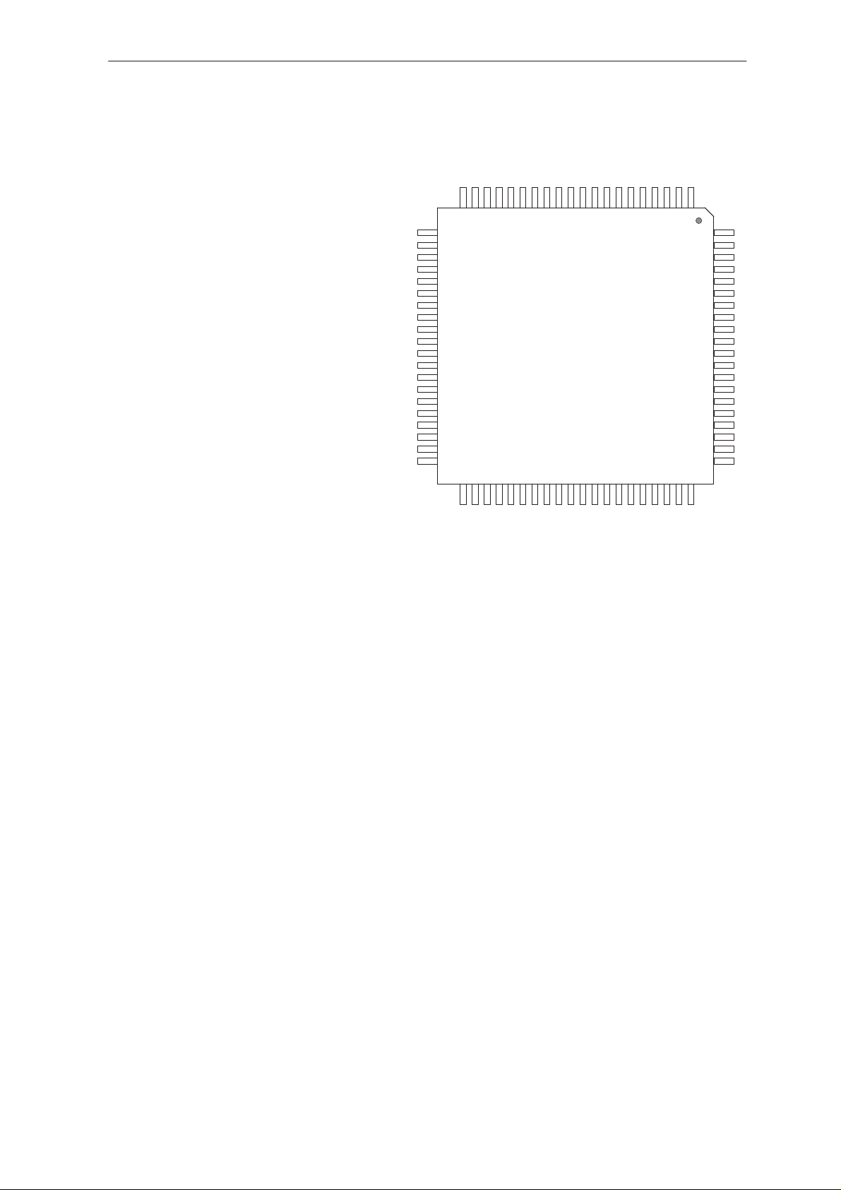
BASEBAND FILTER (N2) IF + FM DETECTOR (D1)
BASEBAND FILTER N2
NC
NC
AVDD
AVSS
NC
NC
11
12
13
14
15
N2
16
17
18
19
20
Q_A33
Q_AAFI
AGND
I_AAFI
IF AMP+FM DETECTOR D1
I_A33
10
9
NC
CAL
8
DVDD
7
MC
6
DVSS
5
PD
4
XPD
3
NC
2
Q_PFO
1
1 Capacitor Input (I–channel)
2 RXI Output (I–channel)
3 RX_FIL_CAL CALlibration start
4 Digital VDD
5 9.8304 MHz Master Clock
6 Digital VSS
7 Connected to Ground
8 Power Down, Active low
9 No Connection (Grounded)
10 RXQ Output (Q–channel)
Schematics/Layouts & Pinouts
11 Capacitor Input (Q–channel)
12 No Connection (Grounded)
13 Input (Q–channel)
14 No Connection (Grounded)
15 Analog VDD
16 Analog signal GrouND for external stabilation
17 Analog VSS
18 No Connection (Grounded)
19 No Connection (Grounded)
20 Input (I–channel)
AF OUT
QUAD
IF OUT
RSSI
NC
NC
GND
MIX IN
8
9
7
10
6
11
5
12
D1
4
13
14
3
15
2
16
1
2 x SYNTH (N300)
FAST
CPPF
CPP
VDD1
VDD2
PRI
DGND
FXTAL
PDN
NC
1
2
3
4
5
6
7
8
9
10
20
19
18
17
16
15
14
N300
13
12
11
NC
A0N
VCC
CPA
AGND
AUX
ISET
E
DATA
CLK
9 Demodulate signal output
10 Phase shift signal input of FM demodulator
11 Output terminal of IF AMP
12 Output is DC vs Signal level (RSSI)
13 No Connection
14 No Connection
15 GND
16 1st IF signal input
FIL IN
FIL OUT
DEC
IF IN
VCC
MIX OUT
OSC OUT
OSC IN
1 Local oscillator input
2 Local oscillator output
3 Mix output
4 Power supply
5 2nd IF input
6 Decoupling for bias
7 INVERTER AMP output
8 INVERTER AMP input
1 Control input to speed–up main synth
2 Principal synth speed–up charge–pump output
3 Principal synth normal charge–pump output
4 Digital power supply 1
5 Digital power supply 2
6 1 GHz principal synth RF divider input
7 Digital ground
8 Common reference freq input from chrystal ascillator
9 Principal synth power–on input
10 No Connection
11 Serial clock input
12 Serial data input
13 RX_LE Programming bus enable input (active LOW)
14 Regulator pin to set the charge–pump currents
15 Auxiliary synth frequency input
16 Analog ground
17 180MHz Auxiliary synth charge–pump output
18 Supply for charge–pump and DAC circuits
19 Auxiliary synth power–on input
20 No Connection
Original 11/97
Page 5–3
Page 4

NHD–4
PAMS
Schematics/Layouts & Pinouts
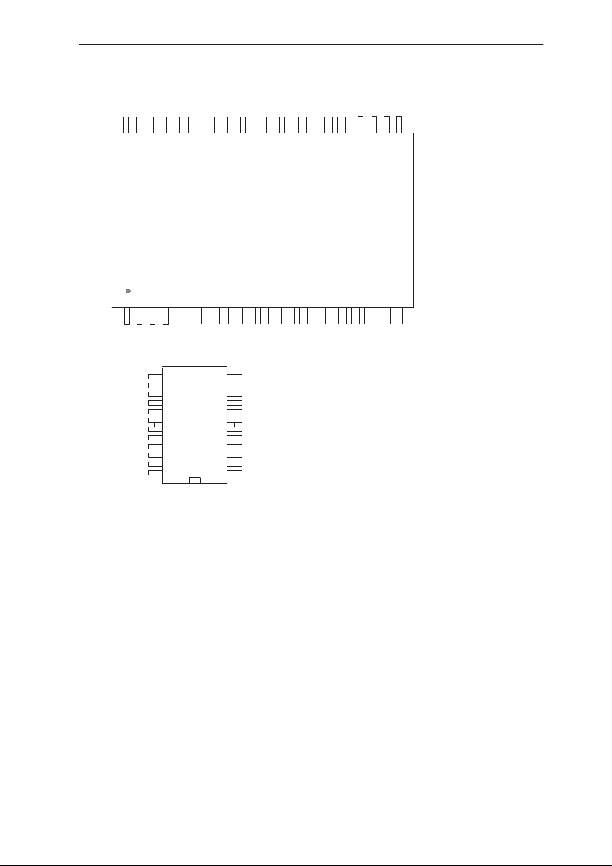
CDAGCR (N1)
C
IF
E
LNA_BP
VCC1
VCC5
GND5
VC
9
10
11
12
13
14
15
VCN
4LON
4LO
VCC8
GND8
GND6
IREF
ICTL
16
17
18
19
20
21
22
23
24
N1
25262728293031
I
Q
SEL1
VCC6
SEL0
GND7
8
7
6
5
4
3
2
1
32
VCC7
VCC4
N4
GND1
IFN
GND2
VCC2
VCC3
GND3
GND4
1 GROUND (Return for CCGA stage 3)
2 GROUND (Return for CCGA stage 2)
3 DC power for CCGA stage 2
4 DC power for CCGA stage 1
5 GROUND (Return for CCGA stage 1)
6 180° IF Input
7 GROUND (Return for LNA)
8 Emitters of QC’s
Technical Documentation
17 Bypass for CCGA’s conrtol line
18 180° Clock Input
19 0° Clock Input
20 DC power for LO circuitry
21 GROUND (Return for LO circuitry)
22 GROUND (Return for DeMod circuitry)
23 Input control current reference
24 Input control current
9 Collector’s of Q1
10 Sets bias current for the internal LNA (short=6.2mA)
11 Emitters of Q1 (Internal LNA)
12 Bypass for LNA’s bias line
13 DC power for LNA
14 DC power for gain control
15 GROUND (Return for Gain control)
16 Bypass for CCGA’s conrtol line
25 DC Power for DeMod circuitry
26 Baseband 90° output
27 Baseband 0° output
28 Set high for –14 dB change in total gain
29 Set high for –7 dB change in total gain
30 GROUND (Return for Outputs Buffers)
31 DC power for Output Buffers
32 DC power for CCGA stage 3
Page 5–4
Original 11/97
Page 5
PAMS
NHD–4
Technical Documentation
MCU (D706)
1 No Connection
2 No Connection
3 MCUREAD : Goes Low to indicate that the
CPU is reading external address
4 MCU_WR : Goes Low to indicate that the
CPU is writing external address
5 Power VL1
6 Ground
7 Ground
8 Connected to VL1
9 Connected to VL1
10 XSYS_RESET : A low input causes chip to reset
11 MCU Non Maskable Interrupt
12 Ground
13–20 MCUDA An 8–bit input/output port
21–28 MCUAD An 8–bit input/output port
29 Ground
30–41 MCUAD An 8–bit input/output port
41 MCUDA
42 Power VL1
43 XPWROFF 8–bit Timer Clock input? ? ? ?
44 TEMP1–EN Power Amp temperature
45 TEMP2_EN VCTCXO temperature
47 CALL LED On when phone is ringing / silent alarm
46 No Connection
48 CODEC_CLK
49 CODEC_DO MCU data write to Codec
50 CODEC_DI MCU data read from Codec
51 Ground
52 VBATDET
53 VCHRGMON
54 HOOK_RXD2 Accessory &
55 BTEMP Battery temparature monitoring
56 RFTEMP 1 for PA , 2 for VCTCXO
57 BTYPE Battery type and size
58 RSSI Amps received signal strenght indicator
59 JCONN External audio input from accescories or external
handsfree microphone
60 VREF
Schematics/Layouts & Pinouts
STBY
MD1
MD2
RES
NMI
Vss
D0
D1
D2
D3
D4
D5
D6
D7
7
8
9
10
11
12
13
14
15
16
17
18
19
20
A0
A1
A2
A3
A4
A5
A6
A7
Vss
A8
A9
A10
A11
A12
A13
A14
A15
A16
A17
A18
21
22
23
24
25
26
27
28
29
30
31
32
33
34
35
36
37
38
39
40
414243444546474849
FTI1
TMCI
Vcc
A19
FTI2
NC
MCU
50
FTOA1
FTOB3/FTCI3
FTOB2/FTCI2
FTOP1/FTCI1
515354
AN1
AN0
AVss
AN2
61 BACKLIGHT Keypad backlight on
62 XCODEC_CS Codec chip select
63 PHFS_TXD2 Power Hans Free / Flash data
64 HOOK_RXD2 Accessory on/off / Flash data
65 Vibra battery controlling
66 MBUS OUT Prosessor monitores outsend data
67 MBUSDET Mbus monitoring during sleepmode
68 No Connection
69 MCU_CLK Clock 15.36 MHz
70 No Connection
71 Ground
72 No Connection
73 No Connection
74 VAHS provides power to Headset
75 5VOFF to 4.7V Regulator (D500)
76 VCHRGPWR controls charging current
77 MCU_INTO
78 No Connection
79 VOLTLIM for future use based on charging
80 XMCU_AS
MD0
RD
NC
WR
Vcc
2
3
4
5
6
55525657585960
AN7
AN6
AN5
AN4
AN3
1
NC
AVcc
AS
80
TMO
79
IRQ1
78
IRQ0
77
WAIT
76
BREQ
75
BACK
74
E
73
NC
72
Vss
71
XTAL
70
EXTAL
69
Vref
68
RXD1
67
TXD1
66
PW3
65
PW2
64
PW1
63
FTOA3
62
FTOA2
61
Original 11/97
Page 5–5
Page 6

NHD–4
PAMS
Schematics/Layouts & Pinouts
Technical Documentation
MCU memory Flash (D709), EEPROM (D703), SRAM (D700)
1
2
3
4
5
6
7
8
9
10
11
12
13
14
15
16
17
18
19
20
1
2
3
4
5
6
7
8
9
10
11
12
13
14
D700 SRAM 32kx8
FLASFM D709 1Mx8
28
27
26
25
24
23
22
21
20
19
18
17
16
15
1
2
3
D703 EEPROM 32kx8
4
5
6
7
8
9
10
11
12
13
14
40
39
38
37
36
35
34
33
32
31
30
29
28
27
26
25
24
23
22
21
28
27
26
25
24
23
22
21
20
19
18
17
16
15
Page 5–6
Original 11/97
Page 7
PAMS
NHD–4
Technical Documentation
DSP memory (D707)
44 43 42 41 40 39 38 37 36 35 34 33 32 31 30 29 28 27 26 25 24 23
D707 SRAM 64kx16
1 2 3 4 5 6 7 8 9 10111213141516171819202122
PSL + (N500)
Schematics/Layouts & Pinouts
DETINCpor
1213
Coff
Creset
VL3l
VL3B
GND
GND
VL2B
VBATSW
VA2
14
15
16
17
18
PSL
19
20
21
22
23
24 VREF
CHRGDET
11
XPWRON
10
XPWROFF
9
XRESET
8
7
GND
6
GND
5
VBAT1VBAT2
4
VL1lVL2l
3
VL1B
2
VA1
1
names beginning with X indicate NOTE:
ACTIVE LOW operation
XPWRON input has internal pull–up resistor
XPPWROFF input has internal pull–down resistor
1 VREF Voltage REFerence output (5mA, ”2%
2 Analog voltage output
3 Base current supply for external transistor (VL1)
4 Output voltage sense from external transistor (VL1)
5 VBATTERY battery voltage
6 Ground (analog/logic)
7 Ground (analog/logic)
8 XPWR_RESET reset control signal to ASIC
9 XPWROFF control input from the MCU
10 XPWRON power on control from UI
11 Battery CHaRGer DETection
12 DETection INput for the supply voltage monitored
13 Connection for an external Capasitor for controlled
Power–ON master Reset
14 Connection for an external timing Capasitor defining
Power–OFF delay
15 Connection for an external timing Capasitor defining
Reset signal delay
16 Output voltage sense from external transistor (VL3)
17 Base current supply for external transistor (VL3)
18 Ground (analog/logic)
19 Ground (analog/logic)
20 Battery Voltage
21 Output voltage sense from external transistor (VL2)
22 Base current supply for external transistor (VL2)
23 VBATDET SWitched VBAT voltage
24 VA2 Analog voltage output (80mA)
Original 11/97
Page 5–7
Page 8
NHD–4
PAMS
Schematics/Layouts & Pinouts
CDAGCT4 (N100)
ICT
24
IREF
VPS2C
GND2D
GND3
VPS3
BRF
RFNOUT
RFOUT
1 180° LO for RF Mixer (Ground with cap)
2 TX_LO 0° LO for RF Mixer
3 GROUND (Return for RF Mixer and Power Amp)
4 TX_PUNC Control for active/power–down modes
5 GROUND (Return for IF LO circuitry)
6 DC power for IF LO circuitry
7 180MHz 2*IF Frequency Input (Ground with cap)
8 180MHz 0° 2*IF Frequency Input
25
26
27
28
29
30
31
32
1
LORFN
VPS2B
GND2B
GND2C
21
22
23
N100
3
465
2
LORF
GND3PDGND1
Technical Documentation
VPS4
GND4
GND2A
VPS2A
17
18
19
20
16
I
15
IN
14
VPS1S
13
QN
12
Q
11
GND4
GND1
10
9
8
LOIF
MODE
7
VPS1
LOIFN
17 DC Power for I/Q Modulator
18 GROUND (Return for I/Q Modulator)
19 GROUND (Return for first CCGA)
20 DC Power for first CCGA and Gain Control Circuitry
21 DC Power for second CCGA
22 GROUND (Return for second CCGA)
23 GROUND (Return for third CCGA)
24 TX_ICT Input control current
9 RFE2 Mode select (Between CDMA and Analog)
10 GROUND (Return for IF LO circuitry)
11 GROUND (Return for IF I/Q Modulator)
12 TX_Q_P 0° Baseband ’QUAD PHASE’ input
13 TX_Q_N 180° Baseband ’QUAD PHASE’ input
14 DC Power for Standby circuitry
15 TX_I_P 180° Baseband ’IN PHASE’ Input
16 TX_I_N 0° Baseband ’IN PHASE’ Input
25 TX_IREF Input control current reference
26 DC Power for third CCGA
27 GROUND Return for Gain Control circuits
28 GROUND (Return for RF Mixer and Power Amplifier
29 DC power for RF mixer
30 Bypass pin for Mixer Bias (Ground with cap)
31 180° RF Output
32 0° RF Output
Page 5–8
Original 11/97
Page 9

PAMS
NHD–4
Technical Documentation
CDCONT5 (N201)
RX_Ict
Lim_Adj
NC
NC
NC
60
61
62
63
64
NC
NC
NC
NC
NC
RX_Exp
TX_Exp
Ana_GND
Vref
Vrx90
VRF
Vrx
Vrxs
Vbbf_Pnp_B
Vbbfil
NC
1
2
3
4
5
6
7
8
9
10
11
12
13
14
15
16
CDCONT5
171819202122232425262728293031
NC
RX_Iref
58
59
TX_Ict
TX_Iref
56
57
NC
55
NC
TX_Driver
53
54
TX_Level
Vtx
Ana_GND
50
51
52
TX_Cntrl
49
48
47
46
45
44
43
42
41
40
39
38
37
36
35
34
33
32
Schematics/Layouts & Pinouts
TX_Driver
Vtx
Vtx_Pnp_B
Vrxd
VRF
Vtxs
Vrxa
VCO_GND
CLK
VCO_GND
VCO_in
CHP_Out
VCO_GND
Vcxo
Sub_GND
VCO_Cap_A
NC
NO CONNECTION
1
NO CONNECTION
2
NO CONNECTION
3
NO CONNECTION
4
NO CONNECTION
5
6
Input to RX Multiplier from RX_dB
7
Inpur to TX Multiplier from TX_dB
8
Analog Ground
9
Reference voltage output
10
Regulated voltage for the 90 MHz Frequency
11
Battery voltage supply
12
Regulated Voltage for the Receiver RF Circuits
13
Regulated Voltage for Chrystal Osc and internal Decode logic
14
Pin for external PNP Base connection for Vbbfil
15
Regulated voltage for the BBFIL
16
NO CONNECTION
NO CONNECTION
17
Switch output
18
Reference input to Error Amp.
19
Transmitter power–level information
20
NO CONNECTION
21
Digital Groung
22
Digital control bit for Regulator switching
23
Digital control bit for Regulator switching
24
Digital Groung
25
Digital control bit for Regulator switching
26
Digital control bit for Regulator switching
27
Digital control bit for Regulator switching
28
29
Vrxd by–passed supply for PLL digital logic
Ground for Charge Pump circuit
30
31
Vrxd by–passed supply for VCO and Clock Buffer
32
Pin for VCO capacitor
TXI
TXI_Ref
TXFM_Cap
NC
Dig_GND
Reset
TX_Punc
Rfe1
Rfe2
Dig_GND
Rfe0
VPLL_Vrxs by–pass
CHP_GND
VCO_Cap_B
VCO_Vrxd by–pass
Pin for VCO capacitor
33
Substarate Groung
34
15.36 MHz clock reference
35
VCO Ground
36
Charge Pump Output
37
VCO input from CHP_Out
38
VCO Ground
39
9.8304 MHz clock output
40
VCO Ground
41
Regulated Voltage for the AMPS circuits
42
Regulated Voltage for the TX LO buffer
43
Battery voltage supply
44
Regulated Voltage for the AGC circuits CDAGCR & CDCONT
45
Pin for external PNP Base connection for Vtx
46
NO CONNECTION
47
NO CONNECTION
48
NO CONNECTION
49
Regulated voltage for the Transmitter circuits and CDAGCT (Pin 47)
50
Output of Driver for Power Amp.
51
Analog Ground
52
Negative input of the Driver circuit for Power Amp. (Pin 48)
53
NO CONNECTION
54
NO CONNECTION
55
56
Control current for CDAGCT
57
Reference current for CDAGCT
58
NO CONNECTION
59
Reference current for CDAGCR
60
Control current for CDAGCR
61
Indicator for Limiter
62
NO CONNECTION
63
NO CONNECTION
64
NO CONNECTION
Original 11/97
Page 5–9
Page 10

NHD–4
PAMS
Schematics/Layouts & Pinouts
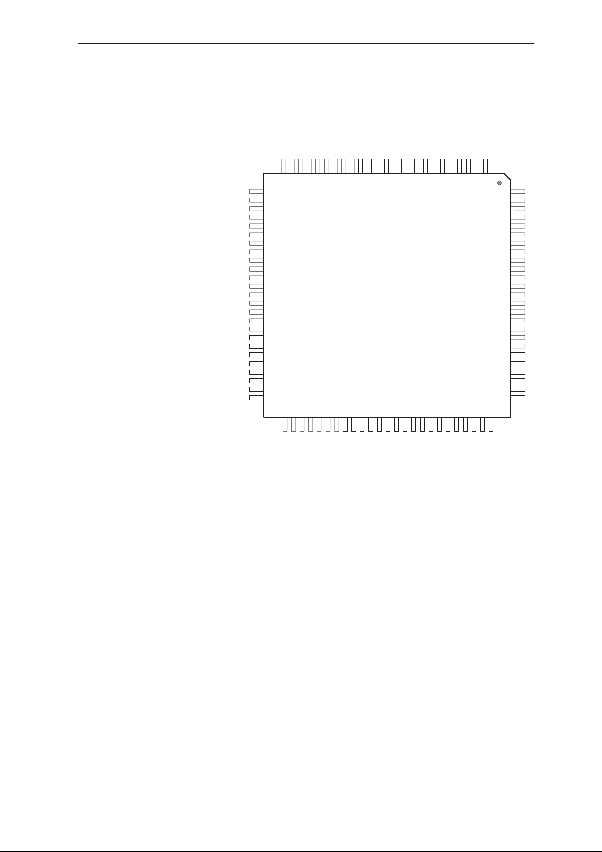
CDRFI (N700)
RXQ5
VDDD3
CLKOUT
VDDD4
VSSD4
VCLKOUT
59
60
61
62
63
64
VCLKIN
VDDD5
CLKIN
VSSA
1
TXAGC1
VDDA1
RXAGC1
VDDA2
VREFP
RXQ
VSSA2
VREF
RXI
TEST
VSSA3
ANATX
1
2
3
4
5
6
7
8
9
10
11
12
13
14
15
16
171819
CDRFI
VERSION 6.0
2122232425262728293031
20
RXQ4
58
RXQ3
57
RXQ2
56
RXQ1
55
RXQ0
54
RXI5
53
RXI4
52
RXI3
51
RXI2
50
RXI1
49
32
Technical Documentation
48
47
46
45
44
43
42
41
40
39
38
37
36
35
34
33
RXI0
EXTVCLKEN
VSSD3
9.8M
VSSD2
EXTTXENA
TDX7
TDX6
TDX5
TDX4
TDX3
TDX2
TDX1
TDX0
IQSELECT
VDDD2
TXI+
1 15.36MHz VCLock recovery INput
2 Digital Power VL3
3 9.83MHz CLock recovery INput
4 Analog Ground
5 TX_GAIN TX AGC control
6 Analog Power VL3
7 RX_GAIN RX AGC control
8 Analog Power VL3
9 Positive Voltage REFerence bypass
10 RX_Q RX signal Quadrature–phase
11 Analog Ground
12 Voltage REFerence bypass
13 RX_I RX signal In–phase
14 TEST input (Not used)
15 Analog Ground
16 MOD ANAlog mode TX signal
SDI
TXI –
VDDA3+4
TXQ+
TXQ –
VSSA4
ANARX+DAF
VSSD1
DAFOUT
SDO
XRESET
SENABLE
SCLK
R/WSEL
VDDD1
17 TX_I_P TX signal In–phase +
18 TX_I_N TX signal In–phase –
19 Analog Power VL3
20 TX_Q_P TX signal Quadrature–phase +
21 TX_Q_N TX signal Quadrature–phase –
22 Analog Ground
23 DAF ANAlog mode RX+DAF signal
24 Analog Ground
25 DAF OUTput
26 CDRFI_SI Serial data In
27 CDRFI_SO Serial data Out
28 XSYS_RESET Whwen set = 0
29 CDRFI_SEN Serial data ENABLE
30 CDRFI_RWSEL Read/Write SELect
31 CDRFI_SCLK Serial data CLock
32 Digital Power VL3
33 Digital Power VL3
34 CDRFI_IQSEL TX IQ SELECT
35–42 TXD TX Data bit 0–7
43 CDRFI_GATE EXTernal TX ENAble
44 Digital Ground
45 CDRFI_9.8MHz clock
46 Digital Ground
47 VCO_EN EXTernal VCLK ENAble
48 No Connection
49–53 RXI RX In–phase data bit 1–5
54 No Connection
55–59 RXQ RX Quadrature–phase data bit 1–5
60 Digital Power VL3
61 9.38M_IN CLocK recovery OUTput
62 Digital Power VL3
63 V15.36M_IN CLocK recovery OUTput
64 Digital ground
Page 5–10
Original 11/97
Page 11

PAMS
NHD–4
Technical Documentation
CDSB 4.5 (D704)
tmtestmode _1
VDDext
132
131
133
VSSext
134
cdRfe_2
cdRfe_3
135
136
ccRXI_1
137
ccRXI_0
138
ccRXQ_4
139
ccRXQ_3
140
ccRXQ_2
ccRXQ_1
141
142
ccRXQ_0
143
ccRXI_4
ccRXI_3
144
145
ccRXI_2
146
VDDint
147
rfClock15M36
148
VSSint
cdRfe_1
149
cdRfe_0
150
151
VDDext
VSSext
152
153
cdTXD_2
cdTXD_1
154
cdTXD_0
155
cdTXD_7
156
157
cdTXD_6
158
cdTXD_5
cdTXD_4
159
160
cdTXD_3
161
VDDint
rfClock9M8
162
163
VSSint
164
cdlQsl
165
ccAData
166
ccSdi
167
ccSdo
cdResetX
168
169
cdSenable
170
cdRWsl
171
cdSClk
172
cdRXle
173
cdSynthData
174
cdSynthClk
cdRfiClk9M81
175
176
VDDext
12345
cdAfc
cdTxiRef
cdVctcxoEn
cdTxGate
mcuRstrobeX
127
128
129
130
126
678
cdTxb
rfSleepClk
cdTxGainAdj
osc_select
122
123
124
125
9
1011121314
cdirq0X
121
cdRxSlp
cdTxc
119
120
VDDint
VSSint
118
cdRfe_7
cdAgcRef
cdTxSlp
115
11691117
114
tmSe
cclfclk
112
113
cdDSync
111
VDDext
VSSext
109
110
cdFlashslX
cdRXenable
107
108
ASIC
CDSB4.5
23
151617
202122
18
19
2425262728
Schematics/Layouts & Pinouts
rfLimAdj
cdRfe_6
cdNMI
ccNoxw
mcuAddpg_0
mcuAddpg_1
cdMcuClk
VSSint
104
105
29
mcuAddpg_3
VDDint
102
101
103
30
31
32
100
33
cdRfiGate
cdAttenable
98
99
mcuAddpg_2
96
97
tmChrgint
92
93
94
95
VDDext
mcuAstrobeX
cdSramslX
mcuData_7
mcuData_6
mcuData_5
mcuData_4
mcuData_3
mcuData_2
mcuData_1
mcuData_0
cdPort0_4
mcuAdd_1
mcuAdd_2
mcuAdd_3
mcuAdd_4
mcuAdd_5
mcuAdd_0
cdTxenable
VDDext
cdPort0_5
mcuMbusdet
cdPort1_7
cdPdm1
cdRomslX
mcustrobeX
tmDBusin
cdPort0_3
cdPort0_2
cdPort0_1
cdPort0_0
cdPort1_6
cdPort1_5
VSSext
35
36
34
373839
40
414243
cdRfe_5
106
tmTestmode_0
rfLimOn
90
osc_zi
VSSint
VDDint
VSSext
tmTck
VSSint
VDDint
cdFS
cdMClk
osc_en
VSSext
89
88
87
86
85
84
83
82
81
80
79
78
77
76
75
74
73
72
71
70
69
68
67
66
65
64
63
62
61
60
59
58
57
56
55
54
53
52
51
50
49
48
47
46
45
44
tmPurX
VSSext
dspDsx
dspAddrL_3
dspStorobeX
dspReadWriteX
Original 11/97
cdint1X
cdDClk
dspAddrL_2
dspAddrU_14
cdint2X
cdRfe_4
VDDint
cdDspClk
VSSint
dspAddrL_1
dspAddrL_4
dspAddrL_5
dspAddrL_6
dspAddrL_0
dspAddrL_7
VSSext
VDDext
dspAddrU_15
VDDint
cdPdm2
dspData_0
dspAddrL_8
dspData_1
dspData_6
dspData_2
dspData_3
osc_out
dspData_4
dspData_5
dspData_7
osc_in
cdPort1_0
cdPort1_1
cdPort1_2
Page 5–11
cd98le
cdPort1_3
cdPort1_4
VDDext
Page 12

NHD–4
PAMS
Schematics/Layouts & Pinouts
1 GND
2 XPWR_RESET Power on Reset
3 XDSP_STRB DSP External memory strobe
4 DSP_RXW DSP Write enable
5 XDSP_DS DSP data select
6–8 DSPAD DSP Lower address
9 DSP_MCLK DBUS 512KHz Clock
10 DSP_CLK DSP Interrupt request 0
11 DSP_CLK DSP Interrupt request 1
12 RX_FIL_CAL Output soursing rfRX_FIl _CAL
signal
13 VL1
14 DSP_CLK DSP clock output 15.36MHz
15 GND
16–21 DSPAD DSP Lower address
22 VL1
23 GND
24–25 DSPAD DSP Upper address
26 DSPDA DSP data bus
27 VL1
28 No Connection
29–35 DSPDA DSP data bus
36 32.768Khz Clock osc. circuit
37 32.768Khz Clock osc. circuit
38–42 LCD_COL GPIO port 1
43 No Connection
44 VL1
45 GND
46 Connected to VL
47–52 LCD_COL GPIO port 1
48 GPIO Port 1
49–52 GPO port 0
53 CODEC_MCLK Codec clock 512KHz
54 CODEC_FS Codec Sync 8KHz
55 DBUS Line in
56 XMCU_WR MCU Write enable
57 XROM_CS ROM select bit
58 No Connection
59 No Connection
60 VL!
61 GND
62 Connected to VL1
63 MBUSDET Mbus activity detect
ASIC CDSB 4.5
65 VL1
66 GND
No Connection
67
68–73 MCUAD MCU Lower address bus
74 VL1
75 GND
76 No Connction
77–84 MCUDA MCU Data bus
85 XSRAM SRAM select bit
86 XMCU_AS MCU Address valid strobe
87 No Connection
88 VL1
89 GND
90 Connected to GND
No Connection
91
92 CHRG_INT Charg interrupt
93 CDRFI_GATE Signal to control Transmitt
mode with in CDRFI
94 SWAGC Signal to control gain switching
Tx power greater than that set by TXI_REF
95
96 MCUAD MCU Upper address bus
97 No Connection
98 MCU_NMI Non Maskable interrupt
99 No Connection
100–102 MCUAD MCU Upper address bus
103 VL!
104 MCU_CLK Clock output 15.36MHz
105 GND
106 No Connection
107 XFLASH_CS Flash select bit
108 No Connection
109 VL1
110 GND
111 DSP_SYNC DBUS 8KHz Sync Clock
112 Connected to GND
113 No Connection
114 RX_CAL Output sourcing rfRX_CAL signal
115 AGC_REF Auxilliary AGC PDM
116 TX_SLOPE PDM
117 VL1
118 GND
119 RX_SLOPE PDM
120 TX_OFFSET PDM
Technical Documentation
122 TXB PDM output signal
123 RX_OFFSET PDM
124 Sleep Clock
125 Connected to VL1
126 TXI_REF PDM output signal
127 AFC PDM output signal
128 VCO_EN VCTCXO enable
129 TX_PUNC Signal to turn off TX
130 XMCU_RD Read enable
131 Connected to GND
132 VL1
133 GND
134 RF_RFEN2 Power control to CDCONT
135 FAST Output sourcing rfFast signal
136,137 RXI_ Receive I data
138–142 RXQ Receive Q data
143–145 RXI_ Receive I data
146 VL1
147 15.36M_IN Clock
148 GND
149 RFEN1 Power control to CDCONT
150 RFEN0 Power control to CDCONT
151 VL1
152 GND
153–160 TXD_ Multiplexed Tx I/Q data in dig mode
Bidirectional transfer of data in dig mode
161 VL1
162 9.83M_IN Clock
163 GND
164 CDRFI_IQSEL IQ select signal in dig mode
Address select bit in anal mode
165 DAFOUT Analog mode input data
166 CDRFI__SI Serial data output pin
167 CDRFI__S0 Serial data input pin
168 XSYS_RESET System reset signal
169 CDRFI__SEN Serial data enable
170 CDRFI_RWSEL Read/Write select in anal mode
171 CDRFI_SCLK Serial data clock
172 RX_LE RX Synthesizer enable
173 DATA RX Synthesizer serial data
174 CLK Synthesizer serial clock
175 CDRFI_9.8M Clock
176 VL1
Page 5–12
Original 11/97
Page 13

PAMS
NHD–4
Technical Documentation
AUDIO CODEC (N600)
VL1
CDO
GND
FS
MCLK
LO
MIC2N
MIC2P
GND
MIC3N
MIC3P
16
17
18
19
20
21
CODEC
22
23
24
25
26
27
28
1 Not connected
2 VA2 Power supply for the analog section
3 VA2 Power input for power section
4 Not connected
5 Not connected
6 XEAR_HFJPWR External earpiece output VF+
7 EarN Differential / earpiece amp outputs
8 EarP Differential / earpiece amp outputs
9 Power Ground
10 PCMIN Receive data input
11 CODEC_CLK Control Clock Input
12 XCODEC_CS Chip Select Input
13 CODEC_DI Control data Input
14 BUZZER Pulse widht modulated buzzer driver output
1415
13
12
11
10
9
8
7
6
5
4
3
2
1
Schematics/Layouts & Pinouts
BZ
CI
CSDX
CCCLK
DR
GND
VLRP
VLRN
VFEARP
VFEANRMIC1N
NCMIC1P
VA2
VA2
NC
15 VL1 Power supply input for the digital section
16 CODEC_DO Control Data output
17 PCM Transmit data output
18 Digital Ground
19 CODEC_FS Frame Synch Input
20 CODEC_MCLK Master Clock Input
21 MICENX A logic written into DO (CR1) appears at LO pin as logic 0 (and vice versa)
22 2nd neg high impedance input to transmit pre–amplifier microphone connection (Connected via cap to Ground)
23 XMIC_JCONN 2nd pos high impedance input to transmit pre–amplifier microphone connection
24 MicN Neg high impedance input to transmit pre–amplifier microphone connection
25 MicP Pos high impedance input to transmit pre–amplifier microphone connection
26 Analog Ground
27 3th neg high impedance input to transmit pre–amplifier microphone connection (Connected via cap to Ground)
28 3th pos high impedance input to transmit pre–amplifier microphone connectionr (Connected via cap to Ground)
Original 11/97
Page 5–13
Page 14
NHD–4
PAMS
Schematics/Layouts & Pinouts
DSP (D705)
1 Ground
2–7 Parallel port address bus
8 VL2
9 Ground
10 Ground
11 +VDD
12 External access ready to complete
13 No connection
14 Data space select
15 No connection
16 Read/write
17 External memory access strobe
18 No Connection
19 No Connection
20 No connection
21 No Connection
22 No conneection
23 Connected to VL2
24 Connected to VL2
25 Connected to Ground
26 Ground
27 Serial port 0 receive clock
28 Serial port 1 receive clock
29 Serial port 0 receive frame synchronization
30 Serial port 1 receive frame synchronization
31 Serial port 0 data receive
32 serial port 1 data receive
33 Serial port 0 transmit clock
34 Serial port 1 transmit clock
35 Ground
36 VL2
37 Serial port 0 transmit frame synchronization
38 Serial port 1 transmit frame synchronization
39 VL2
40 Ground
41 Serial port 0 transmit output
42 Serial port 1 transmitt output
43 No Connection
44 Connected toVL2
45 Interrupt 0
46 Interrupt 1
48 Connected to VL2
49 Connected to VL2
50 Ground
DVSS
CLKR0
CLKR1
FSR0
FSR1
CLKX0
CLKX1
CVSS
CVDD
FSX0
FSX1
DVDD
DVSS
IACK
/
/
/
/
/
CVDD
CVSS
IOSTRB
HOLDA
HOLD
BIO
23
24
CLKMD2
CLKMD3
MSC
IAQ
XF
18
19
20
21
22
55525657585960616263646566676970717374
CNT
TOUT
EMU1/OFF
EMU0
DR0
DR1
DX0
DX1
NMI
INT0
INT1
INT2
INT3
MP/MC
25
26
27
28
29
30
31
32
33
34
35
36
37
38
39
40
41
42
43
44
45
46
47
48
49
50 76
515354
CLKMD1
51–53 Connected to Ground
54 No Connection
55–62 No Connection
63 Ground
64 VL2
65 Ground
66 No Connection
67 No Connection
68 Oscillator/exeternal clock clock input
69 Device reset
70–75 Parallel data port
MSTRB
17
TDO
R/W
16
TDI
Technical Documentation
READY
CVSS
CVDD
CVSS
CVDD
PS
DS
IS
9
10
11
12
13
14
15
A13
A14
A15
5
6
7
8
DSP CI5
68
/TRST
TCK
TMS
CVSS
CVDD
CLKOUT
X1
X2/CLKINRSD0D2D1D3D4
DVSS
76 VL2
77–86 Parallel data port
87 VL2
88 Ground
89 Ground
90 VL2
91–100 Parallel port address bus
A12
4
72
CVSS
A10
A11
123
100
75
D5
A9
99
A8
98
A7
97
A6
96
A5
95
A4
94
A3
93
A2
92
A1
91
A0
90
DVDD
89
DVSS
88
CVSS
87
CVDD
86
D15
85
D14
84
D13
83
D12
82
D11
81
D10
80
D9
79
D8
78
D7
77
D6
DVDD
Page 5–14
Original 11/97
 Loading...