

Page 1

Programme’s After Market Services
NHD–4 Series Transceivers
Chapter 4
System Module
Original 11/97
Page 2

NHD–4
System Module
Technical Documentation
CONTENTS
Baseband Block Connections 4–5. . . . . . . . . . . . . . . . . . . . . . . . . . . . . . . . . . . . . .
Internal Signals and Connections 4–5. . . . . . . . . . . . . . . . . . . . . . . . . . . . . . . .
Power Block 4–5. . . . . . . . . . . . . . . . . . . . . . . . . . . . . . . . . . . . . . . . . . . . . . .
MCU Block 4–6. . . . . . . . . . . . . . . . . . . . . . . . . . . . . . . . . . . . . . . . . . . . . . . .
MCU Memory Block 4–7. . . . . . . . . . . . . . . . . . . . . . . . . . . . . . . . . . . . . . . .
DSP Block 4–8. . . . . . . . . . . . . . . . . . . . . . . . . . . . . . . . . . . . . . . . . . . . . . . .
DSP memory Block 4–8. . . . . . . . . . . . . . . . . . . . . . . . . . . . . . . . . . . . . . . . .
CDSB ASIC Block 4–9. . . . . . . . . . . . . . . . . . . . . . . . . . . . . . . . . . . . . . . . . .
CDRFI Block 4–11. . . . . . . . . . . . . . . . . . . . . . . . . . . . . . . . . . . . . . . . . . . . . .
AUDIO Block 4–12. . . . . . . . . . . . . . . . . . . . . . . . . . . . . . . . . . . . . . . . . . . . . .
P.A.M.S
Page No
External Signals and Connections 4–12. . . . . . . . . . . . . . . . . . . . . . . . . . . . . . .
User Interface Connector 4–12. . . . . . . . . . . . . . . . . . . . . . . . . . . . . . . . . . . .
Baseband Functional Description 4–14. . . . . . . . . . . . . . . . . . . . . . . . . . . . . . . . . . .
Power Supply 4–14. . . . . . . . . . . . . . . . . . . . . . . . . . . . . . . . . . . . . . . . . . . . . . . . .
MCU Block 4–15. . . . . . . . . . . . . . . . . . . . . . . . . . . . . . . . . . . . . . . . . . . . . . . . . . .
DSP Block 4–15. . . . . . . . . . . . . . . . . . . . . . . . . . . . . . . . . . . . . . . . . . . . . . . . . . .
CDRFI 4–15. . . . . . . . . . . . . . . . . . . . . . . . . . . . . . . . . . . . . . . . . . . . . . . . . . . . . . .
Audio Block 4–16. . . . . . . . . . . . . . . . . . . . . . . . . . . . . . . . . . . . . . . . . . . . . . . . . .
Transmitter Functional Description 4–16. . . . . . . . . . . . . . . . . . . . . . . . . . . . . . . . . .
Introduction 4–17. . . . . . . . . . . . . . . . . . . . . . . . . . . . . . . . . . . . . . . . . . . . . . . . . . .
TX Gain Limiting 4–17. . . . . . . . . . . . . . . . . . . . . . . . . . . . . . . . . . . . . . . . . . . . . .
CDMA TX Gain Control 4–17. . . . . . . . . . . . . . . . . . . . . . . . . . . . . . . . . . . . . . . .
AMPS TX Gain Control 4–19. . . . . . . . . . . . . . . . . . . . . . . . . . . . . . . . . . . . . . . .
TX PA Bias Control (Dynamic TXB) 4–20. . . . . . . . . . . . . . . . . . . . . . . . . . . . . .
Temperature Compensation 4–20. . . . . . . . . . . . . . . . . . . . . . . . . . . . . . . . . . . .
Circuit Description 4–20. . . . . . . . . . . . . . . . . . . . . . . . . . . . . . . . . . . . . . . . . . . . .
CDAGCT IC (N100) 4–20. . . . . . . . . . . . . . . . . . . . . . . . . . . . . . . . . . . . . . . .
AT–109 Variable Attenuator (V106) 4–21. . . . . . . . . . . . . . . . . . . . . . . . . . .
3rd Stage Amplifier (V112) 4–21. . . . . . . . . . . . . . . . . . . . . . . . . . . . . . . . . . .
Receiver Functional Description 4–24. . . . . . . . . . . . . . . . . . . . . . . . . . . . . . . . . . . .
Introduction 4–24. . . . . . . . . . . . . . . . . . . . . . . . . . . . . . . . . . . . . . . . . . . . . . . . . . .
Antenna and Coaxial Cable (W400) 4–24. . . . . . . . . . . . . . . . . . . . . . . . . . . . . .
Duplexor (Z102) 4–24. . . . . . . . . . . . . . . . . . . . . . . . . . . . . . . . . . . . . . . . . . . .
RF LNA Switches and SWAGC/RX_CAL Control Lines 4–24. . . . . . . . . .
LNA and RX SAW Filter 4–25. . . . . . . . . . . . . . . . . . . . . . . . . . . . . . . . . . . . .
Mixer (T1) 4–26. . . . . . . . . . . . . . . . . . . . . . . . . . . . . . . . . . . . . . . . . . . . . . . . .
Page 4–2
Original 11/97
Page 3

P.A.M.S
NHD–4
Technical Documentation
1st IF AMP (V9) and the Diode Switch (V10) 4–26. . . . . . . . . . . . . . . . . . .
AMPS Receiver 4–27. . . . . . . . . . . . . . . . . . . . . . . . . . . . . . . . . . . . . . . . . . . . . . .
Crystal Filter (Z3) 4–27. . . . . . . . . . . . . . . . . . . . . . . . . . . . . . . . . . . . . . . . . . .
CDMA Receiver 4–28. . . . . . . . . . . . . . . . . . . . . . . . . . . . . . . . . . . . . . . . . . . . . . .
CDMA IF SAW Filter (Z2) 4–28. . . . . . . . . . . . . . . . . . . . . . . . . . . . . . . . . . . .
Synthesizer Functional Description 4–30. . . . . . . . . . . . . . . . . . . . . . . . . . . . . . . . .
Introduction 4–30. . . . . . . . . . . . . . . . . . . . . . . . . . . . . . . . . . . . . . . . . . . . . . . . . . .
PLL IC (N300) 4–30. . . . . . . . . . . . . . . . . . . . . . . . . . . . . . . . . . . . . . . . . . . . . . . .
The VCTCXO Clock (G300) 4–30. . . . . . . . . . . . . . . . . . . . . . . . . . . . . . . . . . . .
The UHF Synthesizer 4–30. . . . . . . . . . . . . . . . . . . . . . . . . . . . . . . . . . . . . . . . . .
The VHF Synthesizer 4–31. . . . . . . . . . . . . . . . . . . . . . . . . . . . . . . . . . . . . . . . . .
AGC Functional Description 4–32. . . . . . . . . . . . . . . . . . . . . . . . . . . . . . . . . . . . . . .
Signal Descriptions 4–32. . . . . . . . . . . . . . . . . . . . . . . . . . . . . . . . . . . . . . . . . . . .
15.36 MHz 4–32. . . . . . . . . . . . . . . . . . . . . . . . . . . . . . . . . . . . . . . . . . . . . . . .
System Module
DC Voltage Supplies 4–34. . . . . . . . . . . . . . . . . . . . . . . . . . . . . . . . . . . . . . . .
Parts List GR1_17A 4–37. . . . . . . . . . . . . . . . . . . . . . . . . . . . . . . . . . . . . . . . . . . . . .
Original 11/97
Page 4–3
Page 4

NHD–4
System Module
P.A.M.S
Technical Documentation
This page intentionally left blank
Page 4–4
Original 11/97
Page 5
P.A.M.S
NHD–4
Technical Documentation
Baseband Block Connections
Below is a list of the functional blocks of the baseband architecture:
– Power Supply Charging Logic Device (PSL+3)
– Microcomputer Unit (MCU)
– MCU External Memory –
Electrically Eraseable Programmable Read Only Memory (EEPROM)
Static Random Access Memory (SRAM)
Flash Memory
– Digital Signal Processor (DSP)
– DSP External Memory –
Static Random Access Memory (SRAM)
– CDSB ASIC
– CDMA RF to BB Interface (CDRFI)
System Module
– Audio Coder/Decoder (CODEC)
Internal Signals and Connections
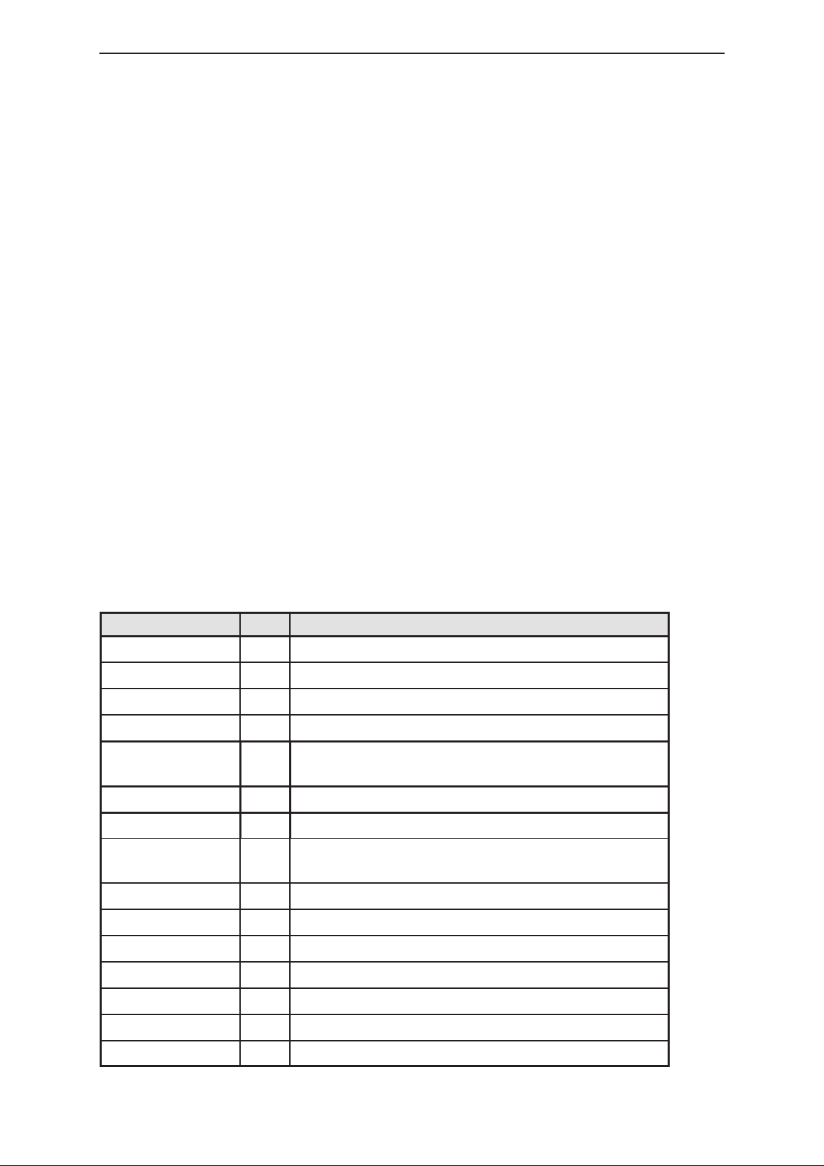
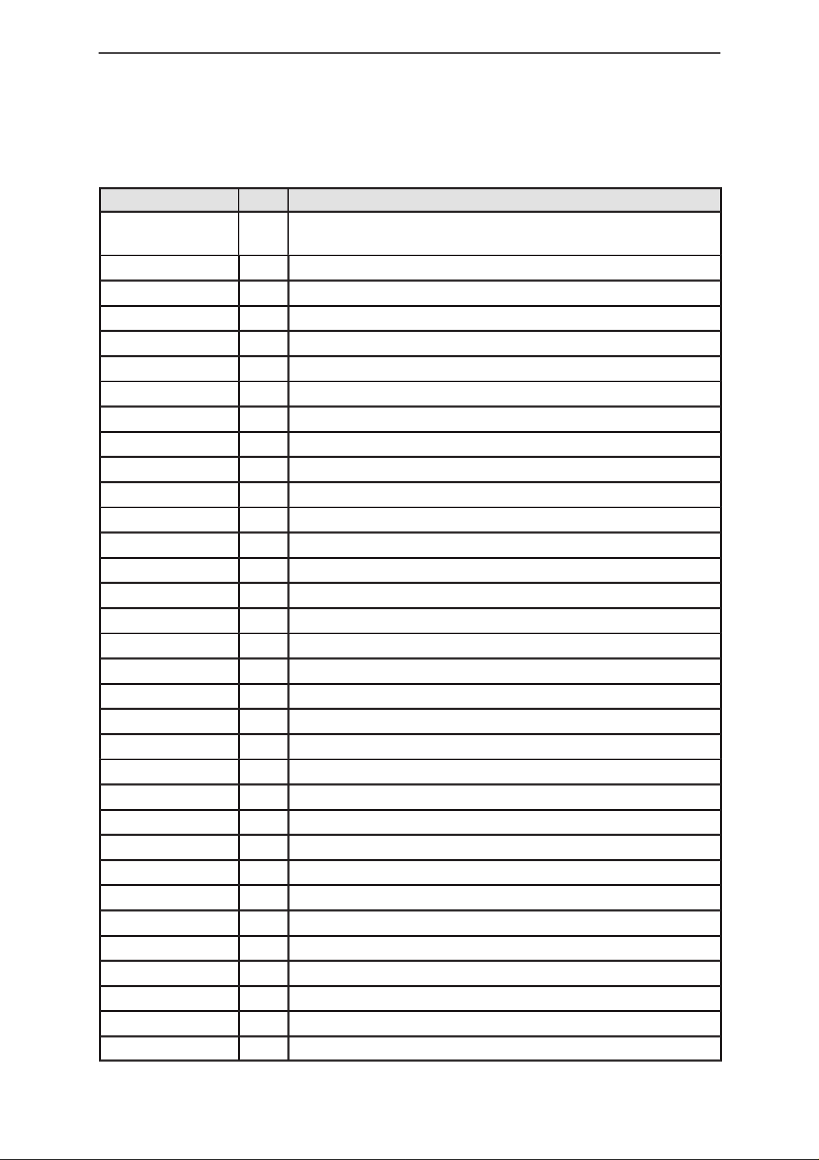
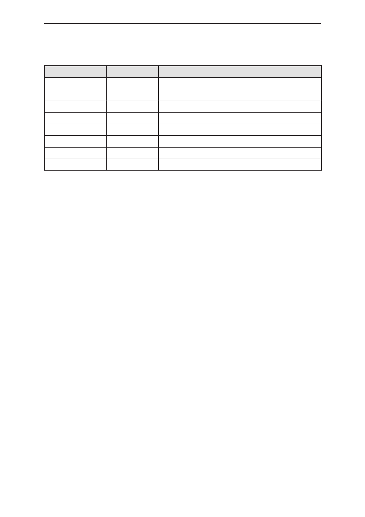
Power Block
Table 1. Power Block Connections
Signal Name T ype Notes
XPWRON IN PWR on switch
XPWROFF IN Power off control
VBATT IN Battery voltage
VCHAR IN Charging voltage
VOLTLIM IN Voltage Limiting of charging while call is in prog-
ress.
5VOFF IN voltage reg control –ON / OFF
VCHRGPWM IN PWM for controlling battery charging.
XPWR_
RESET
OUT Master reset
VL1 OUT Logic supply voltage 1.
VL2 OUT Logic supply voltage 2.
VL3 OUT Logic supply voltage 3.
VA1 OUT Analog supply voltage 1.
VA2 OUT Analog supply voltage 2.
VREF OUT Reference voltage
VL5VOLT OUT Logic supply voltage for MBUS
Original 11/97
Page 4–5
Page 6
NHD–4
System Module
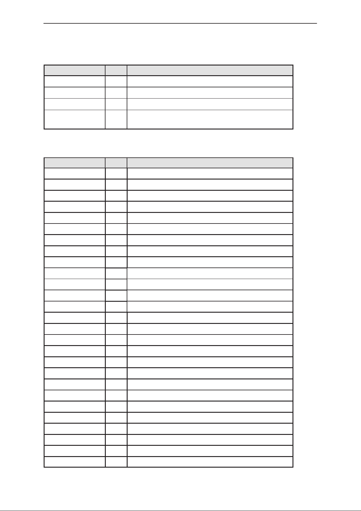
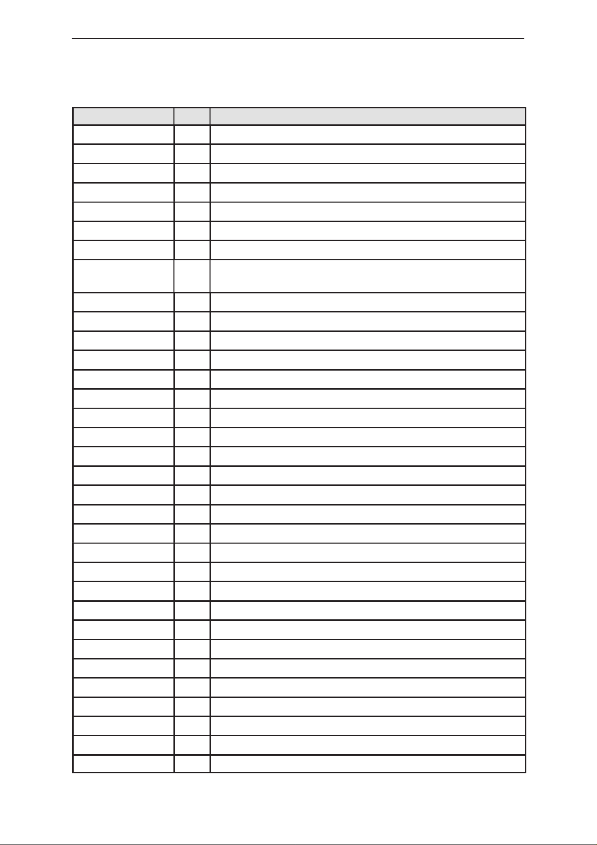
Table 1. Power Block Connections (continued)
NotesTypeSignal Name
Technical Documentation
VLCD OUT Voltage for LCD on UIF
VBATDET OUT Switched VBATT
VC OUT Attenuated VCHRGMON
CHRG_INT OUT Signal to indicate a Charger has been connected
to Phone.
MCU Block
Table 2. MCU Block Connections
Signal Name T ype Notes
MCU_CLK IN Clk into MCU
XSYS_RESET IN MCU Reset
P.A.M.S
MCUAD(19:0) OUT MCU Address Bus
MCUDA(7:0) I/O MCU Data Bus
XMCU_AS OUT MCU Address Strobe
XMCU_RD OUT MCU Read
XMCU_WR OUT MCU Write
MCU_NMI IN MCU Non Maskable Interupt
MCU_INT0 IN MCU Maskable Interupt 1
CODEC_DI OUT Audio codec control data
CODEC_CLK OUT Codec Clock
XCODEC_CS OUT Audio codec chip select
CODEC_DO IN Audio codec control data
CALL_LED OUT UIF CALL_LED enable
BACK_LIGHT OUT UIF BACK_LIGHT enable
PHFS_TXD2 OUT Hands Free speaker Mute Control
HOOK_RXD2 OUT Hook Recieved data
VIB_CONT OUT Vibrator Control
MBUS_OUT OUT MBUS data output
VAHS_EN OUT Headset voltage enable
VOLTLIM OUT Voltage Limiting
5VOFF OUT voltage reg control
VCHRGPWM OUT Control PWM
XPWROFF OUT Watchdog signal
TEMP1_EN OUT RFTEMP1
TEMP2_EN OUT RFTEMP2
VBATDET IN A/D input for battery voltage level
Page 4–6
Original 11/97
Page 7
P.A.M.S
NHD–4
Technical Documentation
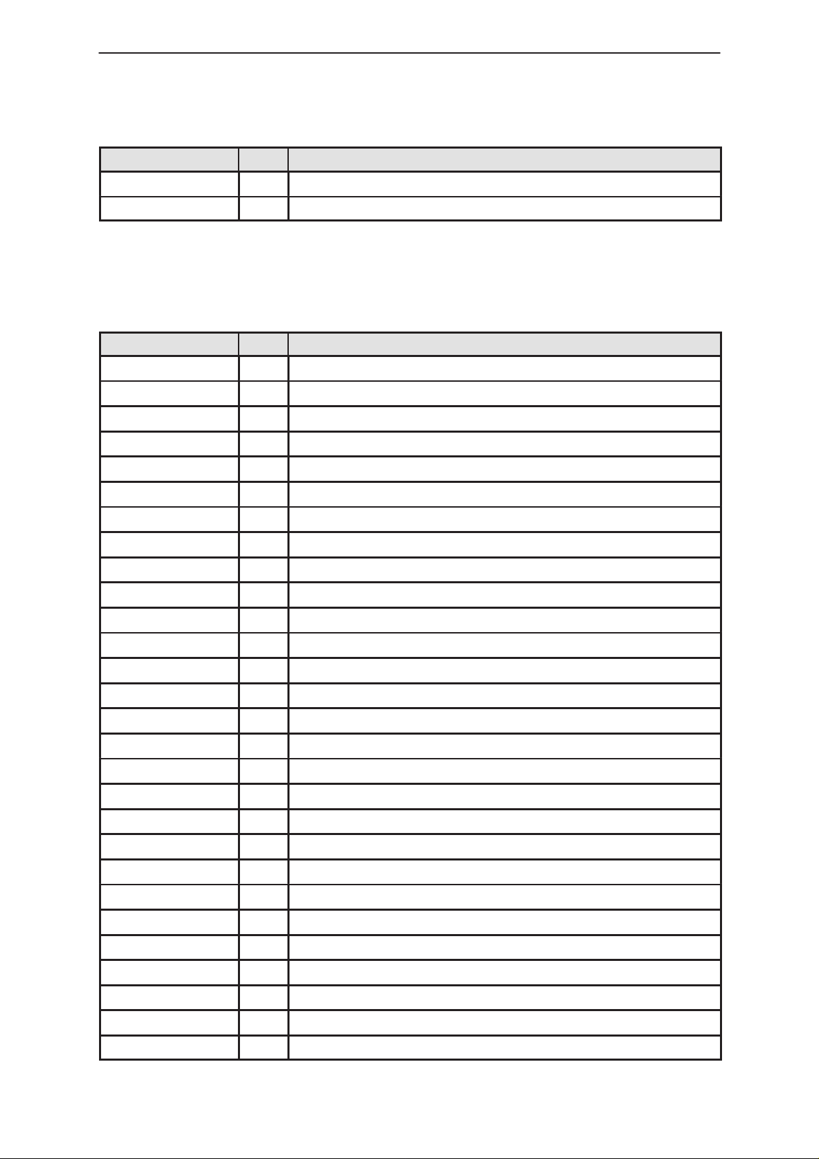
Table 2. MCU Block Connections (continued)
NotesTypeSignal Name
System Module
VCHRGMON IN A/D input for monitoring of charging voltage
HOOK_RXD2 IN A/D input – Hook indicator (Phone on or off Hook)
BTEMP IN A/D input for monitoring Battery temp.
RFTEMP IN A/D input for monitoring RFTEMP 1 and 2 temp.
BTYPE IN A/D input for monitoring Battery type.
RSSI IN A/D input for monitoring RSSI.
JCONN IN A/D input for monitoring Accessory type.
MBUS_DET IN MBUS data input.
MCU Memory Block
Table 3. MCU Memory Block Connections
Signal Name T ype Notes
MCUAD IN MCU Address Bus
MCUDA I/O MCU Data Bus
XMCU_RD IN MCU Read used as Output Enable
XMCU_WR IN MCU Write used as Read/Write select
XFLASH_CS IN Flash Chip Select
XSRAM_CS IN SRAM Chip Select
XROM_CS IN EEPROM Chip Select
Original 11/97
Page 4–7
Page 8
NHD–4
System Module
Technical Documentation
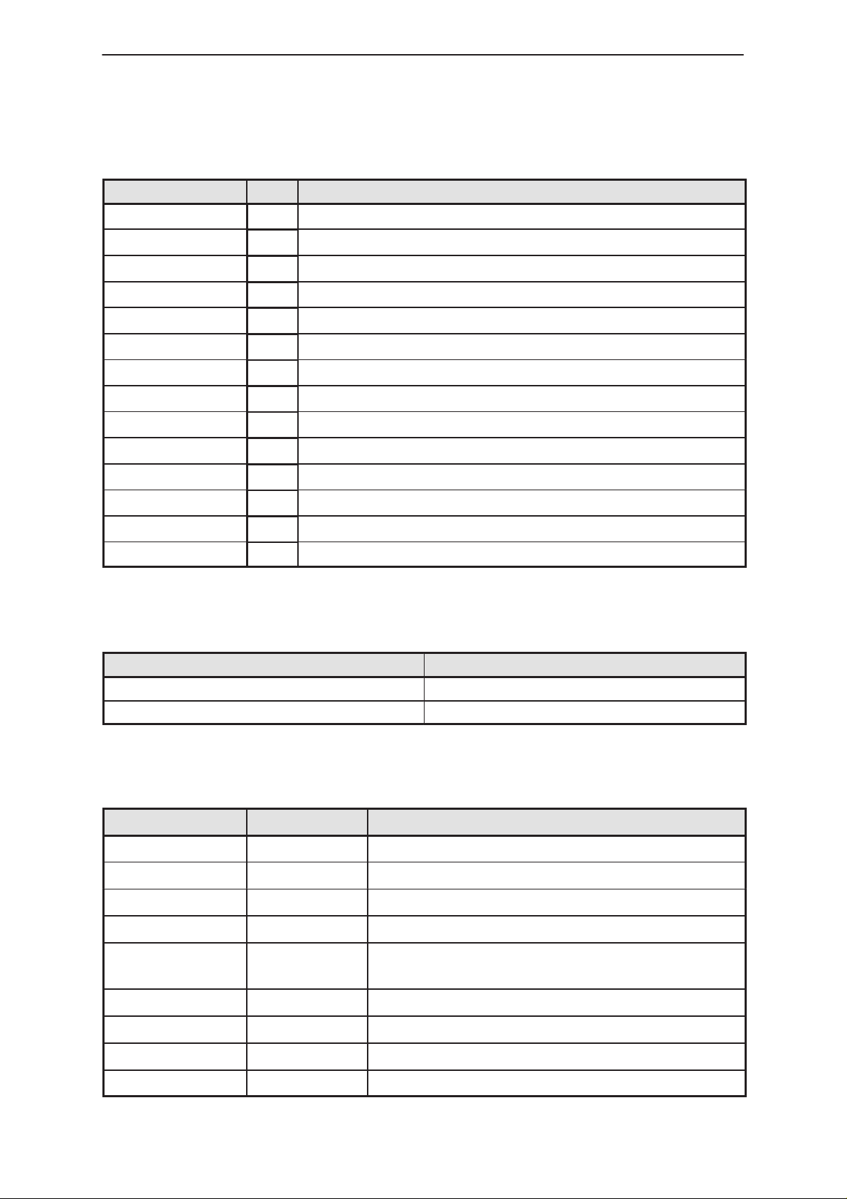
DSP Block
Table 4. DSP Block Connections
Signal Name T ype Notes
DSP_CLK IN DSP Clock
XSYS_RESET IN DSP Reset
DSP_INT0 IN DSP Maskable Interupt 0
DSP_INT1 IN DSP Maskable Interupt 1
DSPAD(15:0) OUT DSP Address Bus
DSPDA(15:0) I/O DSP Data Bus
DSP_RXW OUT DSP Read / Write Select
XDSP_STRB OUT DSP Master Strobe for Memory Access
XDSP_DS OUT DSP Data Strobe for Memory Access
Codec_FS IN Frame Sync
P.A.M.S
Codec_MCLK IN Codec CLK
PCMOUT IN Data from Codec
PCMIN OUT Data to Codec
DSP_SYNC I/O Frame Sync
DSP_MCLK I/O CLK
DBUS_IN IN Data to DSP.
DBUS_OUT OUT Data from DSP.
DSP memory Block
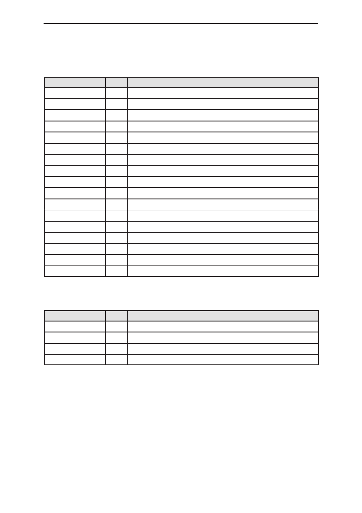
Table 5. DSP Memory Block Connections
Signal Name T ype Notes
DSPAD(15:0) IN DSP Address Bus
DSPDA(15:0) I/O DSP Data Bus
DSP_RXW IN DSP Read / Write Select
XDSP_STRB IN DSP Master Strobe
Page 4–8
Original 11/97
Page 9
P.A.M.S
NHD–4
Technical Documentation
CDSB ASIC Block
Table 6. CDSB ASIC Block Connections
Signal Name T ype Notes
XPWR_
IN Master reset FROM PSL+ 3
RESET
XSYS_RESET OUT System Reset
OSC_OUT IN 32KHz Clk input
OSC_IN IN 32KHz Clk input
CDRFI_SI OUT CDRFI Serial Data In
CDRFI_SO IN CDRFI Serial Data Out
CDRFI_SEN OUT CDRFI Serial data ENABLE
CDRFI_SCLK OUT CDRFI Serial data CLocK
CDRFI_9.8M OUT CDRFI 9.8 MHz clock
System Module
15.36M_IN IN 15.36MHz Clk IN
9.83M_IN IN 9.83MHz Clk IN
TXD(7:0) I/O CDRFI TX Data
CDRFI_RWSEL OUT CDRFI Read/Write SELect
CDRFI_IQSEL OUT CDRFI Tx IQ SELECT
RXQ IN CDRFI RX Quadrature–phase data
RXI IN CDRFI RX In–phase data
DAFOUT IN CDRFI DAF INput
GATE OUT CDRFI
VCO_EN OUT CDRFI
DSP_CLK OUT 7.68 MHz Clk to DSP
DSP_INT0 OUT DSP Maskable Interupt 0
DSP_INT1 OUT DSP Maskable Interupt 1
DSPAD IN DSP Address Bus
DSPDA I/O DSP Data Bus
DSP_RXW IN DSP Read / Write Select
XDSP_STRB IN DSP Master Strobe
XDSP_DS IN DSP Data Strobe
DSP_SYNC OUT Frame Sync
DSP_MCLK OUT CLK
Codec_FS OUT Frame Sync
Codec_MCLK OUT CLK
MCU_CLK OUT 15.36 MHz Clk to MCU
MCUAD(19:0) IN MCU Address Bus
Original 11/97
Page 4–9
Page 10
NHD–4
System Module
Technical Documentation
Table 6. CDSB ASIC Block Connections (continued)
NotesTypeSignal Name
P.A.M.S
MCUDA I/O MCU Data Bus
XMCU_AS IN MCU Address Strobe
XMCU_RD IN MCU Read Enable
XMCU_WR IN MCU Write used as Read/Write select
MCU_NMI OUT MCU Non Maskable Interupt
MCU_INT0 OUT MCU Maskable Interupt 1
MBUS_DET IN MBUS data input.
CHRG_INT IN Signal to indicate a Charger has been connected to
Phone.
XFLASH_CS OUT Flash Chip Select
XSRAM_CS OUT SRAM Chip Select
XROM_CS OUT EEPROM Chip Select
LCD_COL I/O LCD and COL/RO lines to UIF
CDATTEN OUT SW AGC to RF
RF_LIMADJ IN
RF_SCLK OUT Serial Data Clk
RF_SDATA OUT Serial Data
RF_RX_LE OUT Latch Enable for Serial Data
RF_TXB OUT Tx Power Bias
RF_TXREF OUT REF Level for TXIP comparator
RF_AFC OUT VCTCXO control voltage
RF_AGCREF OUT Sets RXI & RXQ levels
RF_TXGAIN OUT Offsets TX gain to RX gain
RF_TXSLP OUT Correction of TX gain slope
RF_RXSLP OUT Correction of RX gain slope
RF_TXC OUT Limit maximum TX gain
RF_TXPUNC OUT
RF_VCO_EN OUT
RF_RFE0 OUT RFEN0
RF_RFE1 OUT RFEN1
RF_RFE2 OUT RFEN2
RF_RFE3 OUT FAST
RF_RFE4 OUT RX_FIL_CAL
RF_RFE5 OUT SEL0
Page 4–10
Original 11/97
Page 11
P.A.M.S
NHD–4
Technical Documentation
Table 6. CDSB ASIC Block Connections (continued)
RF_RFE6 OUT SEL1
RF_RFE7 OUT RF Control Line
CDRFI Block
Table 7. CDRFI Block Connections
Signal Name T ype Notes
XSYS_RESET IN XRESET
SDI IN Serial Data In
SDO OUT Serial Data Out
SENABLE IN Serial data ENABLE
System Module
NotesTypeSignal Name
SCLK IN Serial data CLocK
9.8M IN 9.8 MHz clock
VCLKIN IN VCLocK INput
VCLKOUT OUT VCLocK OUTput
CLKIN IN CLocK INput
CLKOUT OUT CLocK OUTput
TXI+ OUT TX signal In–phase (+)
TXI– OUT TX signal In–phase (–)
TXQ+ OUT TX signal Quadrature–phase (+)
TXQ– OUT TX signal Quadrature–phase (–)
TXD(7:0) I/O TX Data
R/WSEL IN Read/Write SELect
IQSELECT IN Tx IQ SELECT
RXQ IN RX signal Quadrature–phase
RXI IN RX signal In–phase
RXQ(5:0) OUT RX Quadrature–phase data
RXI(5:0) OUT RX In–phase data
TXAGC1 OUT TX AGC control
RXAGC1 OUT RX AGC control
ANATX OUT ANAlog mode TX signal
ANARX+DAF IN ANAlog mode RX + DAF signal
DAFOUT OUT DAF OUTput
GATE IN TBA
VCO_EN IN TBA
Original 11/97
Page 4–11
Page 12
NHD–4
System Module
Technical Documentation
AUDIO Block
Table 8. Audio Block Connections
Signal Name T ype Notes
VA2 IN Analog supply voltage 1. Max 80 mA.
PCMIN IN Received audio in PCM–format
CODEC_FS IN frame sync
CODEC_MCLK IN codec main clock
CODEC_DIN IN Audio codec control data
CODEC_CLK IN Clock for audio codec control data transfer
XCODEC_CS IN Audio codec chip select
HFMIC IN External microphone
MICN, MICP IN Differential microphone signal
PCMOUT OUT Transmitted audio in PCM–format
P.A.M.S
CODEC_DO OUT Audio codec control data
MIC_EN OUT Microphone enable
EXTEAR OUT External received audio
EARN, EARP OUT Internal received audio
External Signals and Connections
Table 9. List of Connectors
Connector Name Notes
User Interface Connector 30 pin ZIF for Flex
System Connector Acc., Charging, Test connector .
User Interface Connector
Table 10. UIF Connector
Signal Name Pin / Conn. Notes
VL1 1 Logic supply voltage
GND 2, 29 Ground
VBAT 3, 30 Battery voltage
BACKLIGHT 4 Backlights on/off
UIF(0:6) 5 – 11 Lines for keyboard write and LCD–controller
control
MIC_EN 12 Microphone bias enable
COL(0:3) 13 – 16 Lines for keyboard read
CALL_LED 17 Call led enable
MICP 18 Microphone (positive node)
Page 4–12
Original 11/97
Page 13
P.A.M.S
NHD–4
Technical Documentation
Table 10. UIF Connector (continued)
NotesPin / Conn.Signal Name
MICN 19 Microphone (negative node)
EARN 20 Earpiece (negative node)
EARP 21 Earpiece (positive node)
BUZZER 22 Buzzer control
ONKEYX 23 Power key
VA1 24 Analog supply voltage
VL5VOLT 26 LCD supply voltage
NC 25,27,28 NO CONNECT
System Module
Original 11/97
Page 4–13
Page 14

NHD–4
System Module
Baseband Functional Description
Below is a list of the functional blocks of the baseband architecture:
– Power Supply
– Microcomputer Unit (MCU)
External Memory –
Electrically Eraseable Programmable Read Only
Memory (EEPROM)
Static Random Access Memory (SRAM)
Flash Memory
MBUS
– Digital Signal Processor (DSP)
External Memory –Static Random Access Memory (SRAM)
DBUS
Multipath Analyzyer
– Audio Coder/Decoder (CODEC)
– CDSB ASIC
Sleep Clock Oscillator (32 KHz)
– CDMA RF to BB Interface (CDRFI)
P.A.M.S
Technical Documentation
Power Supply
The PSL+3 – IC produces the supply voltages:
It also has internal watchdog, voltage detection and charger detection
functions. The watchdog will cut the output voltages if it is not resetted
once in about 6 seconds. The voltage detector resets the phone if the
battery voltage falls below 4.0 V. The charger detection starts the phone if
it is in power–off when the charging voltage is applied.
The charging electronics is controlled by the MCU. When the charging
voltage is applied to the phone while the phone is powered up, the MCU
detects it and starts controlling the charging.
If the phone is in power–off, the PSL+3 will detect the charging voltage
and start the phone. If the battery voltage is high enough the reset will be
released and the MCU will start controlling the charging. If the battery
voltage is too low the phone is in reset and charging control circuitry will
pass the charging current to the battery. When the battery voltage has
reached 4 V the reset will be removed and the MCU starts controlling the
charging. This all is invisible to the user.
– RF Interface
3 * VL 150 mA for logic
VA1 40 mA not used at this time
VA2 80 mA for AUDIO
VREF 5 mA reference
Page 4–14
Original 11/97
Page 15

P.A.M.S
NHD–4
Technical Documentation
MCU Block
The MCU block controls the user interface, link layer, upper layer
protocols, some physical layer tasks, and accessories not linked to data
services. It also executes service and diagnostics commands and
manages the battery.
DSP Block
The DSPU provides control and signal processing for AMPS and CDMA
modes of operation.
– Control and general functions:
– communication with MCU / PC–Locals
– mode control of ASIC hardware
– RF control
– DBUS communication
– AMPS mode speech processing:
– audio signal filtering
– acoustic echo cancellation
– AMPS mode modem functions:
– ST (Signalling Tone) signal generation
– SAT (Supervisory Audio Tone) signal detection and
regeneration
– WBD (Wide Band Data) sending
– Handoff control
– CDMA mode speech processing:
– Vocoder (Voice Coder) encoding and decoding
– acoustic echo cancellation
– CDMA mode control:
– PN (Pseudo Noise) signal acquisition and monitoring
– soft & hard handoffs
– ASIC Rake Receiver demodulator control
– received data rate determination
– Multiplex Sublayer (LM) routing of data to MCU or Voice
Coder
– Loopback and Markov Service Options
System Module
CDRFI
CDRFI is a monolitic CMOS high speed CODEC designed for use in
CDMA (Code Division Multiple Access) Digital Cellular Telephone
applications. It provides AD conversion of the in–phase and quadrature
signals in receive path and generation of the in–phase and quadrature
signals in transmit path. The CODEC interfaces with digital chip(s) via two
parallel interface (separate interfaces for AD and DA signal converters)
and one serial interface (for the control DA converters).
Original 11/97
Page 4–15
Page 16

NHD–4
System Module
Audio Block
The block consists of audio codec with some peripheral components. The
codec includes microphone and earpiece amplifier and all the necessary
switches for routing. The controlling of the codec is done by the MCU. The
PCM–data comes from and goes to DSPs.
The code converts analog voice to digital samples that can be processed
by the DSP. It also accepts DSP processed speech, converts it to analog
and transmits the output to the handset or hands free speaker. The
codec communicates linear coded data with the DSP over a dedicated
serial port. The master clock of the codec is synchronized with the RF
VCTCXO and generated by the CDSB ASIC. Codec set up and DTMF
tone generation are controlled by the microprocessor via a second serial
port.
P.A.M.S
Technical Documentation
Transmitter Functional Description
The transmitter stages are as follows:
The CDAGCT ASIC
The Variable Attenuator
Two SAW filters
Three BJT driver amplifiers
The GaAs FET power amplifier
The Detector circuit
The Isolator
The Duplexer
Page 4–16
Original 11/97
Page 17

P.A.M.S
NHD–4
Technical Documentation
Introduction
NHD–4 uses the same transmitter to up convert, amplify and filter the
analog AMPS and the digital CDMA signals. The key differences between
analog and digital transmission are the Power Amplifier (PA) bias levels ,
attenuation levels of the variable attenuator, and operation of the RF
transmitter ASIC (CDAGCT). It is important to keep in mind that the
AMPS and CDMA signals are significantly different. The AMPS signal is
distinct FM modulated carrier with a channel bandwidth of 30 kHz. CDMA
modulation is spread spectrum. A CDMA signal is 1.23 MHz wide and
appears noise–like.
Aside from this introduction, the Functional Description describes the
various signals entering and exiting the NHD–4 transmitter circuit, as well
as the DC voltage supplies that bias it.
TX Gain Limiting
TX Limiting is a control feature for CDMA TX operation. In some
conditions the AGC loop of the phone may call upon the transmitter to
provide more output power than is recommended for healthy operation.
The TX Limiting circuit places a ceiling or limit on the output power of the
CDMA transmitter. Transmitting above the limit might put the CLY–10 PA
(V113) out of its linear range of operation.
System Module
In CDMA operation the TXI_REF PDM stays fixed at a tuned voltage level.
This tuned level corresponds to the TX output power limit. The tuned
TXI_REF PDM line will be approximately 1.0 V. The detector voltage, TXI,
directly reflects the output power of the TX PA chain (V110–V113). For
maximum CDMA output power TXI is approximately 1.0 V DC at Pin 2.
For minimum CDMA output power TXI is about 2.26 V.
When TXI equals TXI_REF, the LIM_ADJ line goes logic low to
approximately 0.0 V. A way to test CDMA TX Limiting Control is to probe
the LIM_ADJ line with an oscilloscope and maximize the gain of the
transmitter. When the TX output power reaches the limit the LIM_ADJ line
will toggle continuously, appearing as a square wave 3.2 Vpp (read at
R840) with an approximate frequency of 400 Hz.
CDMA TX Gain Control
A fundamental requirement for proper CDMA system operation is that
received signal power levels reaching the digital demodulators remain
constant. This is true for both the mobile unit and the base station. The
mobile unit must dynamically adjust the gain of its receiver to ensure that
the down converted baseband I & Q signal levels delivered to the CDSB
ASIC are always constant. The mobile must also dynamically adjust its
transmit output power so that the base station always receives the same
signal strength. The amount of gain needed at the mobile unit receiver is
used to determine how much gain to provide the mobile unit transmitter,
thus they are linked in a loop.
Original 11/97
Page 4–17
Page 18

NHD–4
Á
Á
Á
Á
Á
Á
Á
Á
System Module
The gain of the CDMA transmitter is controlled by two devices, the
CDAGCT IC (N100) and the AT–109 variable attenuator (V106).
The TX_OFFSET voltage will fall somewhere between 0.0 and 3.15 V,
read at C703. This circuit can be found on the CDCONT schematic. The
resultant voltage is found at the CDCONT IC (N201) at pin 7. The
CDCONT IC interprets this voltage and generates the TX_ICT and
TX_IREF currents.
The gain of the CDAGCT IC (N100) is controlled by the two incoming
currents TX_ICT and TX_IREF. These two signals are currents entering
the IC at pins 24 and 25, through R116 and R115 respectively. The gain
of the IC is set by the ratio of these two current levels. TX_IREF is the
reference current. It stays constant at about 1.0 mA. TX_ICT is the
control current. It varies in as a function of the TX_Gain voltage at the
CDCONT IC.
To measure these currents directly requires that you break the circuit and
input an ammeter. This is impractical in a diagnostics environment.
Instead it is suggested that you simply measure the voltage drop across
R115 and R116 to determine if these signals are correct. The voltage
drop across R115 will remain constant at approximately 100 mV, while the
drop across R116 will vary from approximately 0.0 mV to 100 mV,
depending upon the level of gain required by the AGC system. Below is a
table depicting some sample TX_GAIN and TX_ICT values corresponding
to CDMA TX output power levels.
P.A.M.S
Technical Documentation
CDMA TX Output
БББББ
RF Signal Level
(dBm)
БББББ
TX_GAIN Voltage
БББББ
at C213
БББББ
(V)
TX_ICT Control
БББББ
Current
БББББ
(mA)
TX_ICT
БББББ
(as voltage drop
across R116)
БББББ
(mV)
23
15
10
–5
–20
–35
1.72
1.78
1.80
1.87
1.93
2.00
0.860
0.700
0.560
0.298
0.171
0.093
86.0
70.0
56.0
29.8
17.1
9.3
The Service Software provides a manual control mechanism which
provides the ability to test this transmitter control functionality. This
mechanism is called CDMA TX Manual Gain Control and is discussed in
the Troubleshooting section of this manual.
The amount of attenuation provided by the AT–109 (V106) is controlled by
the control voltage VC. VC is a function of the AGC_REF PDM via the
circuit centered around the op–amp N202. The N202 op–amp can be
found on the CDCONT schematic. VNEG is used at the inverting input of
N202. VNEG will remain constant, typically at –4.1 V. For minimum
attenuation the AUX AGC PDM voltage is typically 0.75 V, resulting in 3.25
V for VC. For maximum attenuation the AUX AGC PDM voltage is
typically 10.0 mV, resulting in 1.50 V for VC.
Page 4–18
Original 11/97
Page 19

P.A.M.S
Á
Á
Á
Á
Á
Á
Á
Á
Á
Á
Á
Á
Á
Á
Á
Á
Á
Á
Á
Á
Á
Á
Á
NHD–4
Technical Documentation
The auxiliary AGC can be manually adjusted using the AGC_REF PDM
controls found in the Service Software. Below is a table detailing typical
voltages of the AGC_REF PDM and VC, referenced against CDMA TX
output power.
CDMA TX
БББББ
Output Power
(dBm)
БББББ
23
21
19
17
15
The AT–109 is put in its minimum attenuation state for AMPS operation.
During AMPS TX operation the AT–109 control voltage VC will be at its
maximum, 4.35 V, measured at C214. The AGC_REF PDM will be 1.50 V
measured at R222.
AMPS TX Gain Control
AGC_REF PDM
БББББ
(decimal value)
БББББ
0
34
60
79
85
AGC_REF PDM
БББББ
voltage at C716
БББББ
(V)
0.798
0.583
0.456
0.367
0.333
System Module
БББББ
БББББ
VC
at C109
(V)
3.28
2.81
2.53
2.33
2.26
NOTE! Be cautious not to confuse the TXI_REF PDM voltage with the
TX_IREF control current. The names are quite similar, but indeed they
are two different signals.
The TXI_REF PDM has 6 tuned values corresponding to the 6 AMPS
power levels used in mobile operation (2–7). The following is a table of
typical values of TXI_REF PDM and TXI voltages, and TX_ICT currents
for the 6 AMPS power levels. There will be variations from phone to
phone.
AMPS
Power
ÁÁ
Level
ÁÁ
ÁÁ
2
3
4
5
6
7
TXI_REF
PDM Voltage
ÁÁÁÁ
(at R210)
ÁÁÁÁ
(V)
ÁÁÁÁ
1.05
1.56
1.92
2.10
2.20
2.26
TXI_REF
PDM
ÁÁÁÁ
decimal val-
ÁÁÁÁ
ue
ÁÁÁÁ
14
239
187
168
157
152
TXI Detector
Voltage
ÁÁÁ
(at N202,
ÁÁÁ
Pin1)
ÁÁÁ
(V)
1.05
1.56
1.92
2.10
2.20
2.26
TX_ICT
(voltage drop
ÁÁÁÁ
across
ÁÁÁÁ
R116)
ÁÁÁÁ
(mV)
44.2
38.6
30.5
22.3
21.9
17.9
While the phone is in AMPS TX mode the TX_IREF current will remain
constant at approximately 1.0 mA. This current can be read indirectly by
measuring the voltage drop across R115. This drop will be approximately
100 mV.
Original 11/97
Page 4–19
Page 20

NHD–4
Á
Á
Á
Á
Á
Á
Á
Á
БББББ
Á
Á
Á
Á
БББББ
System Module
TX PA Bias Control (Dynamic TXB)
The TXB PDM is used to tune the PA bias current. This PDM voltage
interacts with, VTXS, VNEG and an op–amp internal to the CDCONT IC
(N201) to produce VGG. VGG is the negative voltage supply to the gate
of the CLY–10 PA (V113). As VGG changes, so does the bias current.,
and thus the gain. For minimum bias, the 100 mA case the TXB PDM
voltage will be approximately 1.50 V, and VGG will be about –2.35 V. For
maximum bias, or the 250 mA case, the TXB bias will be approximately
1.40 V and VGG will be about –2.00 V. A chart better depicts this data.
Below are some typical voltages and PDM values for this scenario.
P.A.M.S
Technical Documentation
Bias Case
CDMA TX
Output Pow-
БББББ
БББББ
ÁÁÁÁ
ÁÁÁÁ
Minimum – 100 mA
Maximum – 250 mA
Note: Dynamic TXB is only used in CDMA TX modes. For AMPS operation CLY–10 PA
(V113) bias is to draw 100 mA at low output powers. The output power of the AMPS
transmitter increases, the CLY–10 self–biases from the input signal at the gate, thus increasing the current draw to as much as 320 mA.
The negative voltage generator N200 generates the VNEG voltage.
VNEG comes up when VTXS is active. Both VTXS and VNEG maintain
constant voltage levels while on, 4.45 V and –4.10 V respectively. The
node at R203, R204 and R205 will remain fixed at 2.0 V during the
operation of this circuit. This node is an input to the internal op–amp,
which is pin 53 of the CDCONT IC (N201). The base voltage of V201
tracks the VGG voltage.
Temperature Compensation
A thermister (R141) is mounted closely to the final PA stage CLY–10
(V113). The thermister measures the temperature of the power amplifier
and sends the information to the microprocessor via the RFTEMP1 line.
er
(dBm)
<= 10
>= 23
TXB PDB
at C703
ÁÁÁÁ
(V)
ÁÁÁÁ
1.19
1.11
TXB PDM
(decimal val-
ÁÁÁÁ
ue)
ÁÁÁÁ
228
239
VGG
at C202
ÁÁÁ
(V)
ÁÁÁ
–2.35
–2.00
Circuit Description
CDAGCT IC (N100)
The CDMA Automatic Gain Control Transmitter ASIC, or CDAGCT (N100)
generates the AMPS & CDMA RF signals.
The CDAGCT receives the CDMA baseband I & Q signals from the
CDRFI. These two signals exist upon differential lines, TX_I_N/TX_I_P,
and TX_Q_N/TX_Q_P entering the CDAGCT IC at pins 16, 15 and 13, 12
respectively. These signals can be probed with an oscilloscope at any of
the bypass capacitors in series with these four lines. The level will be
approximately 500 mVpp.
Page 4–20
Original 11/97
Page 21

P.A.M.S
NHD–4
Technical Documentation
Bias voltage to the CDAGCT IC is critical. The bias voltage at pins 6, 14,
17, 20, 21, 26, and 29 should always be approximately 3.9 to 4.0 V.
Should it drop to low, or become to great, the CDAGCT IC will not operate
properly. A loss of gain may also occur. The VTXT regulator supplies
voltage to the CDAGCT IC. VTXT should stay constant at 5.3 V in both
AMPS and CDMA operation. The R103, R104 resistor network together
with V115 keep the bias to the CDAGCT IC fixed at about 3.9 V.
AT–109 Variable Attenuator (V106)
The AT–109 (V106) is an attenuation stage in the RF path immediately
following the CDAGCT IC (N100). The VC voltage to pin 5 of this device
sets the level of attenuation. For minimum attenuation in CDMA mode
(maximum output power) VC will be 3.25 V. For maximum attenuation in
CDMA mode VC is 1.50 V. In AMPS TX mode VC will be approximately
4.35 V throughout the entire dynamic range of the transmitter output.
VTXS biases the AT–109 at pin 4. It should be 4.4 V for both AMPS and
CDMA operation.
SAW Filter (Z100)
System Module
This Surface Acoustic Wave (SAW) filter provides rejection in the RX band
(869 to 894 MHz).
1st and 2nd Gain Stages (V110, V111)
The first gain stage V111 should be biased with approximately 3.85 V on
the collector and 0.73 V on the base. V100 acts as a switch, sourcing
current to V111 when the bias voltage on the emitter resistor goes high to
approximately 4.7 V. V100 should have approximately 3.85 V on its
emitter (pin 3) and 3.30 V on its base (pin 2).
The second gain stage V110 should be biased with approximately 2.70 V
on the collector and 0.73 V on the base. V100 acts as a switch, sourcing
current to V110 when the bias voltage on the emitter resistor goes high to
approximately 4.7 V. V100 should have approximately 2.70 V on its
emitter (pin 6) and 3.30 V on its base (pin 5).
SAW Filter (Z101)
This Surface Acoustic Wave (SAW) filter provides rejection in the RX band
(869 to 894 MHz).
3rd Stage Amplifier (V112)
The third gain stage (V112) is a BJT amplifier in the common emitter
configuration. This stage provides of gain to the TX chain, providing drive
power to the final PA stage, V113.
The third gain stage V112 should be biased with approximately 6.0 V on
the collector and 0.7 V on the base. The dual transistor package V108
acts as a switch, sourcing current to V112 when the voltage to the emitter
resistors goes high to approximately 6.2 V. V108 should have
approximately 6.0 V on its pin 6 emitter and 5.5 V on both bases (pins 2
and 5).
Original 11/97
Page 4–21
Page 22

NHD–4
System Module
CLY–10 Power Amplifier (V113)
For CDMA operation the CLY–10 bias current is increased directly with
increasing output power to ensure linear performance. The bias current is
controlled by changing the gate voltage. For minimum bias, the 100 mA
case, the bias on the gate will be about –2.35 V. For maximum bias, or
the 250 mA case, the bias on the gate will be about –2.00 V. The bias
voltage on the drain will be approximately 6.2 V under all biasing
conditions.
For AMPS The PA bias current is set for 100mA at AMPS power level 7.
The PA bias current increases due to self biasing at power level 2
(approximately 27 dBm output). For AMPS TX operation at power level 2
the gate voltage will be approximately –2.7 V and the drain voltage will be
6.2 V.
PA Bias Circuitry
P.A.M.S
Technical Documentation
The transistor network located at the center of the top of the transmitter
schematic is the current bias to the four gain stages. V109 is the source
of current, drawing energy directly from the battery voltage, VRFT (VRF).
The transistors V102 – V104 serve as switches to control the flow of
current to the gain stages by shutting V109 on and off. Both the VNEG
and TX_PUNC voltages must be active for the current source V109 to be
switched on. TX_PUNC is a logic line from the CDSB ASIC (D704), pin
129. It will be approximately 3.15 V when the transmitter is on. The
negative VGG supply is a function of VNEG. VNEG will be approximately
–4.1 V when the transmitter is switched on.
The transistor pair V105 regulates the collector voltage at V109 to about
6.3 V, The emitter of V109 is biased by VRF, which will be the battery
voltage. When the transistor is on, pin 2 of V104 will be approximately 5.3
V. Pins 3 and 6 will remain fixed at approximately 4.7 V.
Detector (V114)
The PA’s RF output power is sampled by a capacitively coupled schottky
dual diode detector. The dectector produces a DC voltage that is
exponentially proportional to the PA’s RF output power. The DC output
voltage decreases as RF power increases. The typical detector voltage
TXI varies from about 2.3 V for minimum RF power to 0.9 V for maximum
RF power. In AMPS mode the detector voltage at N202, pin 1 is
approximately 1.1 V when the TX is at power level 2. The VTXS supply
biases the detector. This DC supply should be approximately 4.40 V in
both AMPS and CDMA modes.
Note it is unwise to probe the detector @ C173 to read the TXI signal. Doing so will
load it down, providing inaccurate readings. It is better to prove TXI at the buffer amp
N202, pin 1 or 2.
Page 4–22
Isolator (V710)
The Isolator isolates the PA from the Duplexor.
Original 11/97
Page 23

P.A.M.S
NHD–4
Technical Documentation
Duplexor (Z102)
The Duplexor isolates the transmit signal from the receiver path and
permits the phone to transmit and receive signals simultaneously (i.e. Full
Duplex operation). The Duplexor is a three terminal, dual frequency (RX
and TX) bandpass splitter/filter and provides the common antenna
connection to the TX and RX circuits. The transmit signal enters the
Duplexor at the “TX” port and exits from the “ANT” port. The duplexor is
the largest device on the PCB and can be found on the TX schematic.
Thermister (R141)
The thermister R141 changes resistance as a function of its temperature.
The voltage across this device comprises the RFTEMP1 signal to the
MCU.
System Module
Original 11/97
Page 4–23
Page 24

NHD–4
System Module
Receiver Functional Description
Introduction
NHD–4, being a dual mode phone, has essentially two receivers, the
analog AMPS and the digital CDMA. These two receivers share a
common front end and only become distinct in the IF stage after mixing
down to 45 MHz. A diode switch, V10, channels the received signal to the
appropriate receiver. It is important to keep in mind that the AMPS and
CDMA signals are significantly different. The AMPS signal is a FM
modulated carrier with a channel bandwidth of 30 kHz. A CDMA signal is
a 1.23 MHz wide spread spectrum carrier pedastal that appears
noise–like. This functional description is divided into three major sections,
the Front End, the AMPS Receiver and the CDMA Receiver.
Antenna and Coaxial Cable (W400)
P.A.M.S
Technical Documentation
The receiver chain begins at the antenna. The antenna is impedance
matched to the coax with L400 and C400. The coaxial cable, W400,
routes the signal down the length of the phone to the bottom connector.
When no external RF connection is made at the bottom connector (X701),
the received signal is directed back up to the top of the phone via the
second, shorter coax length. When the bottom connector is in place, i.e.
with the car kit, the coax leading to the antenna is taken out of the circuit
and the received RF signal launches in from the external connection. It
then proceeds up the shorter length of coax to the top of the phone and
into the duplexor.
Duplexor (Z102)
The Duplexor, Z102 serves to isolate the transmit signal from the receiver
path, and vice versa. The received signal proceeds from the coaxial cable
W400, through C150 into the Duplexor at the point labeled RFOUT. In the
case of the receiver RFOUT is actually the RF input. The duplexor is the
largest device on the PCB and can be found on the TX schematic. This
signal exits the Duplexor on the opposite side that it entered, at the port
labeled RX_IN. It then proceeds through C762 into the RF LNA Switch,
N702.
RF LNA Switches (N701, N702) and SWAGC/RX_CAL Control Lines
NHD–4 has a low noise amplifier, or LNA that can be switched in and out
of RX chain. The LNA is always on during AMPS RX operation. The
switching operation is accomplished by two RF GaAs switches N701 and
N702.
Page 4–24
Original 11/97
Page 25

P.A.M.S
NHD–4
Technical Documentation
For operation with the LNA ”on”, RF is routed into the first switch, N702 at
pin 5. It exits at pin 7 and enters the LNA through L22. After amplification
the receive signal leaves the LNA through C98 and enters the second RF
switch, N701, at pin 7. The signal exits the second switch through pin 5
and proceeds into the UHF RX SAW (Z1) through C771. Switching
control is accomplished at pins 8 and 1 for both switches. For operation
with the LNA (V12) ”on”, or CDMA Hi–Gain, the RX_CAL line at R783/R6
should be logic ”high” at approximately 2.80 V. The SWAGC line at R830
should be logic level ”low”, approximately 0.00 V. The VCONT2 pins (pin
1) of N701 and N702 should be approximately 3.80 V. The VCONT1 pins
(pin 8) should be approximately 0.0 V.
For operation with the LNA ”off”, RF is routed into the first switch, N702 at
pin 5. It exits at pin 2 and enters a resistive matching network through
C787, consisting of R827, R834, and R828. It leaves this network through
C804 and enters the second RF switch, N701, at pin 2. The signal exits
the second switch through pin 5 and proceeds into the UHF RX SAW (Z1)
through C771. Switching control is accomplished at pins 8 and 1 for both
switches. For operation with the LNA ”off”, or CDMA Lo–Gain, the
RX_CAL line at R783/R6 should be logic ”low” at approximately 0.00 V.
The SWAGC line at R830 should be logic level ”high”, approximately 3.00
V. The VCONT2 pins (pin 1) of N701 and N702 should be approximately
0.00 V. The VCONT1 pins (pin 8) should be approximately 2.90 V.
System Module
The following truth table details the states of the switches and the LNA
verse the modes of the phone. This table is also found on the RX
schematic.
State
AMPS
CDMA Hi–Gain
CDMA Lo–Gain
RXCAL
RXCAL
1
1
0
0
LNA (V12) and RX SAW Filter (N701)
Current to source this device originates from the V11 network. C98
delivers the amplified UHF RX signal to the second RF switch N701, pin 7.
The output of N701 (pin 5) routes the signal to the UHF RX SAW Filter
(Z1). The UHF signal leaves the SAW at pin 5 and enters the mixer
through C41.
LNA
ON
ON
OFF
OFF
VCONT1
0
0
1
0
SWAGC
0
0
1
0
VCONT2
1
1
0
1
Original 11/97
Page 4–25
Page 26

NHD–4
System Module
Mixer (T1)
The mixer is a three port passive Si device. Of the eight pins, five are
grounded. The remaining three constitute the RF, LO and IF ports. The
received UHF signal enters the mixer at pin 5, the LO port, from C41. The
RX_LO signal originates from the UHF synthesizer and enters the mixer at
pin 8, the RF port, via a microstrip line which runs within the PCB, under
the components on the board. It is 45 MHz greater in frequency than the
received signal. These two incoming signals mix within the device and
produce a 45 MHz IF signal which leaves the mixer at the IF port, pin 4.
It should be noted that the RF and LO ports on the mixer, pins 5 and 8 are
implemented opposite in this circuit to what the device manufacturer has
specified. On the schematic it shows the received RF entering the mixer
at the LO port and the RX_LO entering the mixer at the RF port. This is
not a design flaw. The device works correctly either way.
1st IF AMP (V9) and the Diode Switch (V10)
P.A.M.S
Technical Documentation
After mixing down to the 45 MHz IF frequency the received signal is again
amplified by the 1st IF amplifier, V9. The IF signal leaving the mixer
moves through the matching network L701, C77, L13, and R24 and enters
the base of the transistor V9, pin 3. It exits the collector, pin 1 and
immediately enters the diode switch which routes the signal to either the
AMPS or CDMA receiver.
Bias current to the base of this gain stage differs from AMPS to CDMA
operation. In CDMA mode the VRXM alone supplies base current to V9
through R13 and L11. The voltage at the base, pin 3 should be 1.85 V in
CDMA mode. VRXM should be approximately 4.40 V at R13. In AMPS
operation the dual BJT package V4 and neighboring resistors R4, R5,
R14, and R15 change this bias current when the VRXAM DC voltage
supply comes on. Voltage at the base of V4 (pin 2) is about 2.25 V. The
voltage on the base of V9 (pin 3) should be approximately 1.0 V in AMPS
mode.
Collector biasing of V9 also varies from AMPS to CDMA mode. The
VRXAM DC supply (VRXA from the CDCONT IC) comes on in AMPS
mode. The collector of V9 should be approximately 3.40 V in AMPS
mode.
The collector of V9 should be approximately 3.50 V in CDMA mode.
VRXDM should be about 4.50 V at R23, pin 1.
Page 4–26
Original 11/97
Page 27

P.A.M.S
NHD–4
Technical Documentation
AMPS Receiver
Crystal Filter (Z3)
The 45 MHz AMPS RX IF signal routes through the diode switch and is
filtered by Z3, the crystal filter. L15, C83, C84 and R29 provide matching
and attenuation into the filter. The filtered signal exiting the crystal
proceeds through C14 and into the AMPS RX IC, D1 at pin 16.
AMPS RX IC (D1)
The AMPS RX IC, D1 completes the demodulation of the AMPS signal
with the help of some peripheral circuitry. VRXAM supplies approximately
4.40 V to this IC at pin 4. The 45 MHz IF signal enters at pin 16, the Mixer
In port. The IC supports the active portion of another oscillator circuit
used in the second down conversion, or mixing stage. This 2nd LO runs
at 44.545 MHz. L16, C6, C7, C9, R1 and crystal B1 make up the
resonator circuit of this oscillator. This resonator connects to the IC at
pins 1 and 2.
System Module
The 45 MHz 1st IF signal mixes with the 44.545 MHz LO to produce the
2nd IF signal at 455 kHz. This mixing stage is located within the AMPS
RX IC. The down converted 2nd IF signal exits the mixer at pin 3 of the IC
and is filtered by Z4, the 455 kHz ceramic filter. C5 and C4 help match
the input and output of the filter to the IC at pins 5 and 6.
The 455 kHz 2nd IF FM signal is quadrature demodulated by a circuit
comprised of L17, C85 and R32, all in parallel across pins 4 and 10. It is
important to NOT adjust the tunable inductor L17!!! Doing so will NOT
assist in troubleshooting a faulty receiver, it will only make things
WORSE!!! This device is tuned by its manufacturer to the proper
inductance.
The audio signal remaining exits pin 9 of the IC and proceeds through R2.
C1 and C10 provide some filtering before this signal is A/D converted by
the CDRFI IC, N700. This audio line is labeled ANARX + DA. This signal
may be viewed with an oscilloscope as an audio sine wave of
approximately 380 mVpp. The output frequency will depend upon the
input frequency deviation of the modulated signal entering the phone.
RSSI Indicator Line
Receive signal strength indication (RSSI) is provided via pin 12 of the
AMPS RX IC, D1. As the signal level is increased the voltage at pin 12 or
C13 will also increase. This voltage should be approximately 1.78 V for a
modulated –75 dBm input signal.
Original 11/97
Page 4–27
Page 28

NHD–4
System Module
CDMA Receiver
CDMA IF SAW Filter (Z2)
For CDMA RX operation the 45 MHz IF signal exits the 1st IF amplifier
(V9) through pin 4 of the diode switch (V10). This signal then enters the
CDMA SAW Filter (Z2), passing through an impedance matching network
comprised of L8, L9, C71, C72, and C73. R22 and R23 supply current to
V9 and V10. R22 also serves to set the Q of L8. The SAW filter itself has
a bandwidth of 1.23 MHz. The output at pin 10 is matched to the next
stage via C70 and L7. Two of the ten pins of this device serve as the RF
input and output, while the other eight are ground. It is extremely
important that all ten pins are well soldered to the PCB.
1CDMA IF LNA Stage (V7)
The received CDMA IF signal goes through another stage of amplification
before being down converted to baseband by the CDAGCR IC (N1). V7 is
this gain stage, a BJT in common base configuration. V8 temperature
compensates the base voltage to V7 at the junction of R19, R20 and R21.
The IF signal leaves this amplifier through the collector, pin 1. It enters
the CDAGCR IC (N1) at pin 8, passing through an impedance matching
network L4 and C69. In CDMA RX operation about 0.60 V should be
found on the emitter of V7, pins 2 and 4. The collector will have about
1.40 V. The collector and base of V8 will be approximately 0.7 V.
P.A.M.S
Technical Documentation
CDAGCR – CDMA Receiver IC (N1)
The CDAGCR IC (N1) serves two functions. It controls the gain (AGC) of
the received CDMA signal, and it quadrature demodulates the 45 MHz IF
signal, and at the same time brings the IF down to baseband frequencies.
The dynamic gain of the CDAGCR IC (N1) is controlled by the two
incoming signals RX_IREF and RX_ICT. These two signals are currents
entering the IC at pins 23 and 24, through R17 and R16 respectively.
RX_IREF is the reference current. RX_ICT is the control current. It varies
in accordance with the gain required of the IC.
To measure these currents directly requires that you break the circuit and
input an ammeter. This is impractical. Instead it is suggested that you
simply measure the voltage drop across R17 and R16 to determine if
these signals are correct. The voltage drop across R17 will remain
constant at approximately 360 mV, while the drop across R16 will vary
from approximately 10 mV to 115 mV. A simple test to demonstrate the
functionality of the CDMA receiver AGC is found in the Troubleshooting
portion of this document. This test also provides a table detailing the
voltage drops (currents) generated verse received RF signal levels.
The DC supply VRXD provides bias to this IC. This supply will be
approximately 4.40 V when the phone is in CDMA mode. When
troubleshooting be sure to check all eight pins.
Page 4–28
The demodulated baseband digital I and Q signals exit the CDAGCR IC at
pins 26 and 27 and proceed to the BFILCT IC (N2) through C33 and C57.
Original 11/97
Page 29

P.A.M.S
NHD–4
Technical Documentation
Either of these two signals can be viewed with an oscilloscope. With an
RF input of 881.62 MHz CW into a CDMA receiver tuned to channel 384,
either of these signals will appear as sine waves of approximately 190
mVpp magnitude, 100 kHz in frequency.
BFILCT (N2)
The BFILCT IC, N2 serves to filter the demodulated baseband I & Q
signals before delivering them to the CDRFI IC (N700) for A/D conversion.
This IC also amplifies the I & Q signals. The I & Q signals enter this IC at
pins 13 and 20 via C33 and C57 respectively. During normal operation
pin 3 of N2 will be pulsed about every 10 seconds by the RX_FIL_CAL
signal. The VBBFILM DC supply should be approximately 3.10 V at C36,
C55 or C56. About 3.00 V should exist at the pin 8, R791, R792 node.
System Module
Original 11/97
Page 4–29
Page 30

NHD–4
System Module
Synthesizer Functional Description
Introduction
The synthesizer module generates the oscillations necessary for the
operation of the phone. It provides the clock signal for digital ICs and it
creates the UHF and VHF oscillations needed to up convert and down
convert the baseband signals to RF frequencies. There are three
synthesizers in the NHD–4 phone. Only two will be discussed here, the
UHF and 180 MHz VHF. The third, a 9.8304 MHz clock oscillator, is
discussed in the CDCONT/AGC Functional Description.
The UHF and 180 MHz VHF oscillations are generated by phase lock
loops. The 15.36 MHz VCTCXO (G300) is the reference oscillator for all
frequency synthesis.
PLL IC (N300)
P.A.M.S
Technical Documentation
The core of the NHD–4 synthesizer is the PLL IC (N300). This IC
supports two independent PLL circuits, both of which are used in NHD–4.
The primary synthesizer is used to generate the tunable UHF LO. The
secondary synthesizer generates a constant 180 MHz VHF signal. The IC
is programmed by three lines; RX_LE, DATA, and CLK. There are three
DC voltage supply pins on this device. Pins 4 and 5 should be
approximately 3.15 V, and Pin 18 should be 4.15 V.
The VCTCXO Clock (G300)
A 15.36 MHz VCTCXO (G300) creates the common reference frequency
(clock) for the synthesizers, as well as the remainder of the phone.
Biasing this device requires 3.60 V on pin 4, V
signal is routed to the PLL IC (N300) pin 8, CDRFI IC (N700), and
CDCONT IC (N201).
The UHF Synthesizer
The operating frequency range of the UHF synthesizer is 914.01 to
938.97 MHz, or AMPS channels 990 to 799. This synthesizer has two
modes of operation, Normal and Fast. Normal mode is the default, while
Fast mode allows the synthesizer to lock to frequency faster. Fast mode
is activated with the Fast line held active high. The output of the UHF
passive loop filter is a DC voltage of 1.0 to 3.0 volts that tunes the VCO
(G301) at the “C” pin. The VCO (voltage controlled oscillator) (G301)
generates the UHF LO. The “B” pin of the VCO should be biased with
approximately 4.25 V, supplied from VRXS via R808. VRXS should be
approximately 4.15 V at R808 when the phone is in AMPS mode.
DD. The 15.36 MHz clock
Page 4–30
The output RF power from the VCO is routed to two gain stages and back
to the PLL IC pin 6 to close the phase locked loop. The two gain stages
amplify the UHF LO signal and provide it to the RX and TX modules
respectively.
Original 11/97
Page 31

P.A.M.S
NHD–4
Technical Documentation
N704 is biased at pin 3 by approximately 3.40 V, supplied from VRX via
R803. VRX should be about 4.40 V. The RX_LO signal is routed to the
mixer (Z1) through a SAW filter (Z701).
N705 is biased at pin 3 to approximately 2.70 V, from VTXT through R809
and R815. VTXT should be approximately 4.40 V. The TX_LO signal is
delivered to the CDAGCT IC (N100) pin 2, through C795.
The VHF Synthesizer
The second PLL frequency synthesizer is the VHF, generating a constant
180 MHz. The varactor diode also doubles as an FM modulator for AMPS
TX operation. The 180 MHz output of the oscillator is amplified by the
common base buffer amp (V303).
The voltage at junction of R313 and the cathode of the varactor diode
(V301) should always be a constant voltage somewhere between 1.5 V
and 3.0d V. The base, emitter and collector of the oscillator transistor
(V302) should be 2.32 V, 1.73 V, and 2.56 V respectively. The buffer
amplifier (V303) is biased up with 4.30 V at the collector, 3.33 V at the
base, and 2.62 V at the emitter. All these voltages originate from VRX90
which ought to be about 4.40 V at R806.
System Module
The ANATX line feeds the AC audio signal from the CDRFI IC (N700) via
C341. When active, this signal can be viewed with an oscilloscope. With
the ST tone active, the ANATX line will have an amplitude of
approximately 250 mVpp at the R317, C341 node. ST (signaling tone)
generates 10 kHz of modulation frequency.
Original 11/97
Page 4–31
Page 32

NHD–4
System Module
AGC Functional Description
Signal Descriptions
Below are descriptions of the signals found within the CDCONT circuitry.
9.8304 MHz
The 9.8304 MHz line is the output of the synthesizer onboard the
CDCONT IC (N201). Measured at C217 this signal should be
approximately 700 mV when measured with an oscilloscope and a high
impedance scope probe. This signal is used to clock the baseband
portions of the phone while operating in CDMA mode.
15.36 MHz
The 15.36 MHz line is the reference frequency input to the synthesizer on
board the CDCONT IC (N201). Measured at the CDCONT side of R319
this signal should be approximately 540 mV when measured with an
oscilloscope and high impedance scope probe. This signal originates
from the VCTCXO (G300).
P.A.M.S
Technical Documentation
AGC_REF
LIM_ADJ
RFEN 0–2
This is a PDM voltage used to control the level of attenuation of the
AT–109 (V106). This signal originates at the CDSB ASIC (D704), pin 115.
Measured at this pin, this PDM will vary from 0 to 3.15 V when moved
over its dynamic range. The ASIC side of R701 would be another good
probe point. Be aware that at this node the voltage will still be pulsed AC,
however a true RMS meter will average out the current to provide the
correct DC voltage.
This control signal is the output of the comparator used in the CDMA TX
Gain Limiting control feature. It signals the CDSB ASIC (D704) when the
maximum allowed CDMA TX output power has been achieved. This
signal can be read at C807. When not at the output power limit, this
signal will be logic high at approximately 3.15 V. When the limit has been
reached this signal will toggle low (0.0 V) and high (3.15 V) at a frequency
of approximately 400 Hz.
The three RFE lines determine the mode of the phone. They originate
from the CDSB ASIC (D704) at pins 150, 149, and 134 for RFE0, RFE1
and RFE2 respectively.
RX_GAIN
Page 4–32
RX_Gain originates at pin 7 of the CDRFI, and is used for CDMA RX Gain
control.
Original 11/97
Page 33

P.A.M.S
NHD–4
Technical Documentation
RX_ICT
RX_ICT is the control current to the CDAGCR IC (N1).
RX_IREF
RX_IREF is the reference control current to the CDAGCR IC (N1).
RX_OFFSET
RX_OFFSET is a PDM voltage. CDSB ASIC (D704) pin 123, this PDM
will vary from 0 to 3.15 V when moved over its dynamic range. The ASIC
side of R712 would be another good probe point.
TX_GAIN
TX_Gain originates at pin 5 of the CDRFI, and is used for CDMA TX Gain
control.
TX_ICT
System Module
TX_ICT is the control current to the CDAGCT IC (N100).
TX_IREF
TX_IREF is the reference control current to the CDAGCT IC (N100).
TX_OFFEST
TX_OFFSET is a PDM voltage. Measured at the CDSB ASIC (D704) pin
120, this PDM will vary from 0 to 3.15 V when moved over its dynamic
range. The ASIC side of R711 would be another good probe point.
TXB
TXB is a PDM voltage. When measured at its origin, pin 122 of the ASIC,
this PDM will vary from 0 to 3.15 V when moved over its dynamic range.
The ASIC side of R703 would be another good probe point.
TXI
The TXI signal is a voltage originating from the Detector (V114). TXI will
be approximately 1.0 V when the phone is transmitting at maximum
power. Note: It is important to never read TXI at the detector, pin 1.
Doing so will load this device down. TXI should be read from N202, pin 1
or 2.
TXI_REF
TXI_REF is a PDM voltage. When measured at its origin, pin 126 of the
ASIC, this PDM will vary from 0 to 3.15 V when moved over its dynamic
range. The ASIC side of R702 would be another good probe point.
VBAT
VBAT is the battery voltage.
Original 11/97
Page 4–33
Page 34

NHD–4
System Module
VC
VC is the control voltage to the AT–109 variable attenuator. VC will
typically be about 3.8 V when signaling the AT–109 for minimum
attenuation, as it does in AMPS mode operation.
VCO_EN
VCO_EN is better known as the Reset line. It originates at the CDSB
ASIC (D704) pin 128. It terminates at the CDCONT IC (N201) pin 23, the
Reset pin.
DC Voltage Supplies
The CDCONT IC (N201) contains the DC voltage regulators, or supplies,
used to provide DC bias throughout the RF modules of the phone. There
are nine regulators. Voltage regulation is performed within the CDCONT
IC for six of these; VRX90, VRX, VRXS, VTXS, VRXD and VRXA. The
remaining three, VTX, VBBFIL, and VRXD_R have some additional
regulation external to the CDCONT. VBAT, the battery voltage, is the
voltage source. These voltage supplies are turned on and off depending
upon the mode of the phone. The table below details the active supplies
and their approximate voltages for operation in both the AMPS RX/TX
mode and the CDMA RX/TX mode. A shaded box indicates that supply is
on for the respective mode. Test points for voltage measurement of the
respective supplies are also listed.
P.A.M.S
Technical Documentation
Mode VBBFIL VNEG VRX VRXA VRXD VRXD_R VRXS VRX90 VTX VTXS
Measurement
point
AMPS RX/TX
CDMA RX/TX
C224 N200
pin 5
~ 0.0 –4.10 4.45 4.45 1.65 ~ 0.0 4.45 4.45 5.30 4.45
3.15 –4.10 4.45 1.20 4.45 4.50 4.45 4.45 5.35 4.45
C206 C219 C218 N706
pin 4
C207 C205 C212 C200
* Values are in volts (V)
VBBFIL
VBBFIL provides bias to the BFILCT2 IC (N2). The VBBFIL voltage
supply circuit uses an external PNP transistor (V203) for regulation. This
supply is on during CDMA RX/TX operation. When VBBFIL is active the
collector of V203 will be approximately 3.15 V, the emitter voltage will be
VBAT, the battery voltage, and the base voltage will be approximately 0.7
V less than the emitter voltage.
VNEG
VNEG is created by the negative voltage generator N200. The VTXS
supply is used as the positive voltage bias from which to generated the
negative voltage. Whenever VTXS is active, VNEG will be present.
VNEG is approximately
Page 4–34
– 4.1 V when VTXS is 4.45 V.
Original 11/97
Page 35

P.A.M.S
NHD–4
Technical Documentation
VRX
VRX is used to supply the LNA (V12) and the LNA switches (N701, N702).
It is also biases the RX_LO gain stage (N704) at the UHF synthesizer
module. VRX will be approximately 4.45 V while active in AMPS RX/TX
mode.
VRXA
VRXA is used for AMPS RX applications such as bias for the AMPS RX IC
(D1) and the 1
approximately 4.45 V when active.
VRXD
VRXD will be approximately 4.45 V while active.
VRXD_R
Both the CDAGCR IC (N1) and the CDMA IF LNA (V7) are biased from
this supply. The 1
System Module
st
IF gain stage while in AMPS operation. VRXA will be
st
IF gain stage (V9) is also biased from this supply.
VRXS
VRX90
VTX
N706 is a voltage regulator IC providing 4.50 V at pin 4 when enabled at
pin 1.
VRXS is used to bias the PLL IC (N300) and the 15.36 MHz VCTCXO
(G300). VRXS should be approximately 4.45 V when active in the AMPS
RX/TX mode.
VRX90 is used to bias the 180 MHz VCO and buffer amp. VRX90 should
be approximately 4.45 V when active in the AMPS RX/TX mode.
VTX is used in transmitter applications, mainly for biasing the CDAGCT IC
(N100).
Just like the VBBFIL, the VTX supply circuit uses an external PNP
transistor (V202) for regulation. The resistors R201 and R202 are used
as part of this external regulator circuit. This supply is on whenever the
transmitter is on. When this supply is active, the collector of V203 will be
approximately 5.30 V, the emitter will be VBAT, the battery voltage, and
the base of V203 will be approximately 0.7 V down from the emitter.
VTXS
VTXS is used in transmitter applications such as bias for the AT–109
variable attenuator (V106) and bias to the Detector (V114). This supply
also biases the negative voltage generator (N200) which creates VNEG.
VTXS will be approximately 4.45 V when active in the AMPS RX/TX mode.
Original 11/97
Page 4–35
Page 36

NHD–4
System Module
9.8304 MHz Synthesizer
The CDCONT IC (N201) contains a PLL frequency synthesizer which
generates a 9.8304 MHz oscillation used to clock the baseband modules
of the phone. The 15.36 MHz VCTCXO is used as the reference
oscillation. VRXD_C (VRXD) supply biases the PLL at pin 29 of N201 via
R212, decoupled with C221 and C222. There should be approximately
4.15 V on Pin 29. The loop filter of the PLL is external to the CDCONT
IC, comprised of R213, R214, C209, C210, and C211. The internal VCO
input, pin 38 should have approximately 1.60 V on it.
In CDMA operation the bias current to the final PA stage (V113) is dynamic. Bias current is set such that the CLY–10 (V113) final PA stage will
draw 100 mA for up to 10 dBm of CDMA TX output power. Above 10
dBm of output the bias changes, ramping up to a maximum draw of 250
mA achieved at 23 dBm of output power. The slope of this ramp is defined as the TXB Slope. The 250 mA current bias is maintained for power
output greater than 23 dBm. This feature is referred to as Dynamic TXB.
The following graph depicts the dynamic relationship between CDMA output power and CLY–10 (V113) bias current.
P.A.M.S
Technical Documentation
Page 4–36
Original 11/97
Page 37

P.A.M.S
NHD–4
Technical Documentation
Parts List GR1_17A
p.n 0200519 EDMS issue 23.0
Item Code Description Value Type
R001 1430790 Chip resistor 27 k 5 % 0.063 W 0402
R002 1430754 Chip resistor 1.0 k 5 % 0.063 W 0402
R003 1430754 Chip resistor 1.0 k 5 % 0.063 W 0402
R004 1430740 Chip resistor 330 5 % 0.063 W 0402
R005 1430758 Chip resistor 1.5 k 5 % 0.063 W 0402
R006 1430796 Chip resistor 47 k 5 % 0.063 W 0402
R013 1430832 Chip resistor 2.7 k 5 % 0.063 W 0402
R014 1430778 Chip resistor 10 k 5 % 0.063 W 0402
R015 1430778 Chip resistor 10 k 5 % 0.063 W 0402
R016 1430740 Chip resistor 330 5 % 0.063 W 0402
R017 1430740 Chip resistor 330 5 % 0.063 W 0402
R018 1430778 Chip resistor 10 k 5 % 0.063 W 0402
R019 1430700 Chip resistor 10 5 % 0.063 W 0402
R020 1430744 Chip resistor 470 5 % 0.063 W 0402
R021 1430762 Chip resistor 2.2 k 5 % 0.063 W 0402
R022 1430748 Chip resistor 680 5 % 0.063 W 0402
R023 1430700 Chip resistor 10 5 % 0.063 W 0402
R024 1430726 Chip resistor 100 5 % 0.063 W 0402
R025 1430693 Chip resistor 5.6 5 % 0.063 W 0402
R028 1430724 Chip resistor 82 5 % 0.063 W 0402
R029 1430734 Chip resistor 220 5 % 0.063 W 0402
R030 1430748 Chip resistor 680 5 % 0.063 W 0402
R031 1430700 Chip resistor 10 5 % 0.063 W 0402
R032 1430766 Chip resistor 3.9 k 5 % 0.063 W 0402
R033 1430754 Chip resistor 1.0 k 5 % 0.063 W 0402
R034 1430710 Chip resistor 22 5 % 0.063 W 0402
R035 1430754 Chip resistor 1.0 k 5 % 0.063 W 0402
R036 1430780 Chip resistor 12 k 5 % 0.063 W 0402
R100 1430744 Chip resistor 470 5 % 0.063 W 0402
R101 1430700 Chip resistor 10 5 % 0.063 W 0402
R102 1430744 Chip resistor 470 5 % 0.063 W 0402
R103 1430708 Chip resistor 18 5 % 0.063 W 0402
R104 1430726 Chip resistor 100 5 % 0.063 W 0402
R105 1430764 Chip resistor 3.3 k 5 % 0.063 W 0402
R106 1430734 Chip resistor 220 5 % 0.063 W 0402
R107 1430766 Chip resistor 3.9 k 5 % 0.063 W 0402
R108 1430776 Chip resistor 8.2 k 5 % 0.063 W 0402
R109 1430764 Chip resistor 3.3 k 5 % 0.063 W 0402
System Module
Original 11/97
Page 4–37
Page 38

NHD–4
System Module
R110 1430720 Chip resistor 56 5 % 0.063 W 0402
R111 1430778 Chip resistor 10 k 5 % 0.063 W 0402
R112 1430786 Chip resistor 18 k 5 % 0.063 W 0402
R113 1430804 Chip resistor 100 k 5 % 0.063 W 0402
R114 1430804 Chip resistor 100 k 5 % 0.063 W 0402
R115 1430726 Chip resistor 100 5 % 0.063 W 0402
R116 1430726 Chip resistor 100 5 % 0.063 W 0402
R117 1430693 Chip resistor 5.6 5 % 0.063 W 0402
R118 1430778 Chip resistor 10 k 5 % 0.063 W 0402
R119 1430780 Chip resistor 12 k 5 % 0.063 W 0402
R120 1430754 Chip resistor 1.0 k 5 % 0.063 W 0402
R121 1430718 Chip resistor 47 5 % 0.063 W 0402
R124 1430772 Chip resistor 5.6 k 5 % 0.063 W 0402
R125 1430732 Chip resistor 180 5 % 0.063 W 0402
R126 1430796 Chip resistor 47 k 5 % 0.063 W 0402
R127 1430796 Chip resistor 47 k 5 % 0.063 W 0402
R128 1430754 Chip resistor 1.0 k 5 % 0.063 W 0402
R129 1430754 Chip resistor 1.0 k 5 % 0.063 W 0402
R130 1430700 Chip resistor 10 5 % 0.063 W 0402
R132 1430732 Chip resistor 180 5 % 0.063 W 0402
R133 1430732 Chip resistor 180 5 % 0.063 W 0402
R134 1430714 Chip resistor 33 5 % 0.063 W 0402
R135 1430746 Chip resistor 560 5 % 0.063 W 0402
R136 1430762 Chip resistor 2.2 k 5 % 0.063 W 0402
R137 1430734 Chip resistor 220 5 % 0.063 W 0402
R138 1430691 Chip resistor 2.2 5 % 0.063 W 0402
R139 1430700 Chip resistor 10 5 % 0.063 W 0402
R140 1430802 Chip resistor 82 k 5 % 0.063 W 0402
R141 1800659 NTC resistor 47 k 10 % 0.12 W 0805
R143 1430754 Chip resistor 1.0 k 5 % 0.063 W 0402
R201 1430790 Chip resistor 27 k 5 % 0.063 W 0402
R202 1430764 Chip resistor 3.3 k 5 % 0.063 W 0402
R203 1430794 Chip resistor 39 k 5 % 0.063 W 0402
R204 1430788 Chip resistor 22 k 5 % 0.063 W 0402
R205 1430804 Chip resistor 100 k 5 % 0.063 W 0402
R206 1430780 Chip resistor 12 k 5 % 0.063 W 0402
R207 1430832 Chip resistor 2.7 k 5 % 0.063 W 0402
R208 1430762 Chip resistor 2.2 k 5 % 0.063 W 0402
R209 1430726 Chip resistor 100 5 % 0.063 W 0402
R210 1430786 Chip resistor 18 k 5 % 0.063 W 0402
R211 1430796 Chip resistor 47 k 5 % 0.063 W 0402
R212 1430700 Chip resistor 10 5 % 0.063 W 0402
R213 1430784 Chip resistor 15 k 5 % 0.063 W 0402
P.A.M.S
Technical Documentation
Page 4–38
Original 11/97
Page 39

P.A.M.S
NHD–4
Technical Documentation
R214 1430774 Chip resistor 6.8 k 5 % 0.063 W 0402
R215 1430786 Chip resistor 18 k 5 % 0.063 W 0402
R216 1430786 Chip resistor 18 k 5 % 0.063 W 0402
R217 1430772 Chip resistor 5.6 k 5 % 0.063 W 0402
R218 1430778 Chip resistor 10 k 5 % 0.063 W 0402
R219 1430754 Chip resistor 1.0 k 5 % 0.063 W 0402
R220 1430700 Chip resistor 10 5 % 0.063 W 0402
R222 1430786 Chip resistor 18 k 5 % 0.063 W 0402
R223 1430778 Chip resistor 10 k 5 % 0.063 W 0402
R224 1430780 Chip resistor 12 k 5 % 0.063 W 0402
R225 1430790 Chip resistor 27 k 5 % 0.063 W 0402
R226 1430788 Chip resistor 22 k 5 % 0.063 W 0402
R228 1430776 Chip resistor 8.2 k 5 % 0.063 W 0402
R229 1430778 Chip resistor 10 k 5 % 0.063 W 0402
R300 1430754 Chip resistor 1.0 k 5 % 0.063 W 0402
R301 1430808 Chip resistor 150 k 5 % 0.063 W 0402
R302 1430798 Chip resistor 56 k 5 % 0.063 W 0402
R307 1430710 Chip resistor 22 5 % 0.063 W 0402
R308 1430718 Chip resistor 47 5 % 0.063 W 0402
R309 1430754 Chip resistor 1.0 k 5 % 0.063 W 0402
R310 1430796 Chip resistor 47 k 5 % 0.063 W 0402
R311 1430802 Chip resistor 82 k 5 % 0.063 W 0402
R312 1430778 Chip resistor 10 k 5 % 0.063 W 0402
R313 1430770 Chip resistor 4.7 k 5 % 0.063 W 0402
R314 1430756 Chip resistor 1.2 k 5 % 0.063 W 0402
R315 1430760 Chip resistor 1.8 k 5 % 0.063 W 0402
R316 1430740 Chip resistor 330 5 % 0.063 W 0402
R317 1430804 Chip resistor 100 k 5 % 0.063 W 0402
R318 1430774 Chip resistor 6.8 k 5 % 0.063 W 0402
R319 1430754 Chip resistor 1.0 k 5 % 0.063 W 0402
R321 1430786 Chip resistor 18 k 5 % 0.063 W 0402
R322 1430762 Chip resistor 2.2 k 5 % 0.063 W 0402
R323 1430700 Chip resistor 10 5 % 0.063 W 0402
R324 1430832 Chip resistor 2.7 k 5 % 0.063 W 0402
R325 1430748 Chip resistor 680 5 % 0.063 W 0402
R326 1800659 NTC resistor 47 k 10 % 0.12 W 0805
R327 1430778 Chip resistor 10 k 5 % 0.063 W 0402
R328 1430792 Chip resistor 33 k 5 % 0.063 W 0402
R329 1430770 Chip resistor 4.7 k 5 % 0.063 W 0402
R331 1430730 Chip resistor 150 5 % 0.063 W 0402
R400 1430724 Chip resistor 82 5 % 0.063 W 0402
R401 1430716 Chip resistor 39 5 % 0.063 W 0402
R500 1430842 Chip resistor 680 k 1 % 0.063 W 0402
System Module
Original 11/97
Page 4–39
Page 40

NHD–4
System Module
R501 1430770 Chip resistor 4.7 k 5 % 0.063 W 0402
R502 1430770 Chip resistor 4.7 k 5 % 0.063 W 0402
R503 1430840 Chip resistor 220 k 1 % 0.063 W 0402
R504 1430796 Chip resistor 47 k 5 % 0.063 W 0402
R505 1430804 Chip resistor 100 k 5 % 0.063 W 0402
R506 1430801 Chip resistor 2.1 k 1 % 0.063 W 0402
R507 1430844 Chip resistor 3.9 k 1 % 0.063 W 0402
R508 1430790 Chip resistor 27 k 5 % 0.063 W 0402
R510 1430730 Chip resistor 150 5 % 0.063 W 0402
R511 1430762 Chip resistor 2.2 k 5 % 0.063 W 0402
R512 1430762 Chip resistor 2.2 k 5 % 0.063 W 0402
R513 1430764 Chip resistor 3.3 k 5 % 0.063 W 0402
R514 1430764 Chip resistor 3.3 k 5 % 0.063 W 0402
R515 1430788 Chip resistor 22 k 5 % 0.063 W 0402
R516 1430726 Chip resistor 100 5 % 0.063 W 0402
R600 1430804 Chip resistor 100 k 5 % 0.063 W 0402
R601 1430792 Chip resistor 33 k 5 % 0.063 W 0402
R602 1430792 Chip resistor 33 k 5 % 0.063 W 0402
R603 1430804 Chip resistor 100 k 5 % 0.063 W 0402
R604 1430726 Chip resistor 100 5 % 0.063 W 0402
R605 1430778 Chip resistor 10 k 5 % 0.063 W 0402
R606 1430780 Chip resistor 12 k 5 % 0.063 W 0402
R607 1430758 Chip resistor 1.5 k 5 % 0.063 W 0402
R700 1430790 Chip resistor 27 k 5 % 0.063 W 0402
R701 1430796 Chip resistor 47 k 5 % 0.063 W 0402
R702 1430770 Chip resistor 4.7 k 5 % 0.063 W 0402
R703 1430790 Chip resistor 27 k 5 % 0.063 W 0402
R704 1430804 Chip resistor 100 k 5 % 0.063 W 0402
R707 1430726 Chip resistor 100 5 % 0.063 W 0402
R708 1430790 Chip resistor 27 k 5 % 0.063 W 0402
R709 1430790 Chip resistor 27 k 5 % 0.063 W 0402
R711 1430792 Chip resistor 33 k 5 % 0.063 W 0402
R712 1430794 Chip resistor 39 k 5 % 0.063 W 0402
R716 1430726 Chip resistor 100 5 % 0.063 W 0402
R717 1430726 Chip resistor 100 5 % 0.063 W 0402
R718 1430726 Chip resistor 100 5 % 0.063 W 0402
R723 1430726 Chip resistor 100 5 % 0.063 W 0402
R724 1430770 Chip resistor 4.7 k 5 % 0.063 W 0402
R725 1430726 Chip resistor 100 5 % 0.063 W 0402
R726 1430840 Chip resistor 220 k 1 % 0.063 W 0402
R727 1430840 Chip resistor 220 k 1 % 0.063 W 0402
R728 1430778 Chip resistor 10 k 5 % 0.063 W 0402
R729 1430754 Chip resistor 1.0 k 5 % 0.063 W 0402
P.A.M.S
Technical Documentation
Page 4–40
Original 11/97
Page 41

P.A.M.S
NHD–4
Technical Documentation
R730 1430726 Chip resistor 100 5 % 0.063 W 0402
R731 1430754 Chip resistor 1.0 k 5 % 0.063 W 0402
R732 1430754 Chip resistor 1.0 k 5 % 0.063 W 0402
R733 1430726 Chip resistor 100 5 % 0.063 W 0402
R734 1430726 Chip resistor 100 5 % 0.063 W 0402
R735 1430726 Chip resistor 100 5 % 0.063 W 0402
R736 1430726 Chip resistor 100 5 % 0.063 W 0402
R737 1430726 Chip resistor 100 5 % 0.063 W 0402
R738 1430754 Chip resistor 1.0 k 5 % 0.063 W 0402
R739 1430726 Chip resistor 100 5 % 0.063 W 0402
R740 1430804 Chip resistor 100 k 5 % 0.063 W 0402
R741 1430700 Chip resistor 10 5 % 0.063 W 0402
R751 1430778 Chip resistor 10 k 5 % 0.063 W 0402
R754 1430726 Chip resistor 100 5 % 0.063 W 0402
R755 1430832 Chip resistor 2.7 k 5 % 0.063 W 0402
R757 1430135 Chip resistor 10 M 5 % 0.063 W 0603
R758 1430778 Chip resistor 10 k 5 % 0.063 W 0402
R759 1430796 Chip resistor 47 k 5 % 0.063 W 0402
R760 1430778 Chip resistor 10 k 5 % 0.063 W 0402
R761 1430145 Chip resistor 100 k 1 % 0.063 W 0402
R762 1430796 Chip resistor 47 k 5 % 0.063 W 0402
R763 1430778 Chip resistor 10 k 5 % 0.063 W 0402
R764 1430804 Chip resistor 100 k 5 % 0.063 W 0402
R765 1430770 Chip resistor 4.7 k 5 % 0.063 W 0402
R775 1430718 Chip resistor 47 5 % 0.063 W 0402
R777 1430718 Chip resistor 47 5 % 0.063 W 0402
R779 1430718 Chip resistor 47 5 % 0.063 W 0402
R781 1430718 Chip resistor 47 5 % 0.063 W 0402
R782 1430778 Chip resistor 10 k 5 % 0.063 W 0402
R783 1430796 Chip resistor 47 k 5 % 0.063 W 0402
R785 1430770 Chip resistor 4.7 k 5 % 0.063 W 0402
R786 1430726 Chip resistor 100 5 % 0.063 W 0402
R790 1430790 Chip resistor 27 k 5 % 0.063 W 0402
R791 1430796 Chip resistor 47 k 5 % 0.063 W 0402
R792 1430788 Chip resistor 22 k 5 % 0.063 W 0402
R798 1430770 Chip resistor 4.7 k 5 % 0.063 W 0402
R799 1430730 Chip resistor 150 5 % 0.063 W 0402
R800 1430730 Chip resistor 150 5 % 0.063 W 0402
R801 1430728 Chip resistor 120 5 % 0.063 W 0402
R803 1430726 Chip resistor 100 5 % 0.063 W 0402
R804 1430724 Chip resistor 82 5 % 0.063 W 0402
R805 1430718 Chip resistor 47 5 % 0.063 W 0402
R806 1430710 Chip resistor 22 5 % 0.063 W 0402
System Module
Original 11/97
Page 4–41
Page 42

NHD–4
System Module
R807 1430710 Chip resistor 22 5 % 0.063 W 0402
R808 1430710 Chip resistor 22 5 % 0.063 W 0402
R809 1430734 Chip resistor 220 5 % 0.063 W 0402
R810 1430710 Chip resistor 22 5 % 0.063 W 0402
R813 1430693 Chip resistor 5.6 5 % 0.063 W 0402
R814 1430693 Chip resistor 5.6 5 % 0.063 W 0402
R815 1430734 Chip resistor 220 5 % 0.063 W 0402
R816 1430778 Chip resistor 10 k 5 % 0.063 W 0402
R817 1430774 Chip resistor 6.8 k 5 % 0.063 W 0402
R818 1430754 Chip resistor 1.0 k 5 % 0.063 W 0402
R819 1430690 Chip jumper 0402
R822 1430690 Chip jumper 0402
R825 1430718 Chip resistor 47 5 % 0.063 W 0402
R826 1430718 Chip resistor 47 5 % 0.063 W 0402
R827 1430744 Chip resistor 470 5 % 0.063 W 0402
R828 1430744 Chip resistor 470 5 % 0.063 W 0402
R830 1430796 Chip resistor 47 k 5 % 0.063 W 0402
R831 1430778 Chip resistor 10 k 5 % 0.063 W 0402
R832 1430754 Chip resistor 1.0 k 5 % 0.063 W 0402
R833 1430700 Chip resistor 10 5 % 0.063 W 0402
R834 1430700 Chip resistor 10 5 % 0.063 W 0402
R835 1430770 Chip resistor 4.7 k 5 % 0.063 W 0402
R837 1430690 Chip jumper 0402
R838 1430804 Chip resistor 100 k 5 % 0.063 W 0402
R839 1430778 Chip resistor 10 k 5 % 0.063 W 0402
R840 1430754 Chip resistor 1.0 k 5 % 0.063 W 0402
R841 1430788 Chip resistor 22 k 5 % 0.063 W 0402
C001 2307816 Ceramic cap. 47 n 20 % 25 V 0805
C002 2307816 Ceramic cap. 47 n 20 % 25 V 0805
C003 2320544 Ceramic cap. 22 p 5 % 50 V 0402
C004 2320544 Ceramic cap. 22 p 5 % 50 V 0402
C005 2320544 Ceramic cap. 22 p 5 % 50 V 0402
C006 2320536 Ceramic cap. 10 p 5 % 50 V 0402
C007 2320744 Ceramic cap. 1.0 n 10 % 50 V 0402
C008 2610100 Tantalum cap. 1 u 20 % 10 V 2.0x1.3x1.2
C009 2320554 Ceramic cap. 56 p 5 % 50 V 0402
C010 2320618 Ceramic cap. 4.7 n 5 % 25 V 0402
C011 2320556 Ceramic cap. 68 p 5 % 50 V 0402
C012 2320552 Ceramic cap. 47 p 5 % 50 V 0402
C013 2320744 Ceramic cap. 1.0 n 10 % 50 V 0402
C014 2320544 Ceramic cap. 22 p 5 % 50 V 0402
C015 2307816 Ceramic cap. 47 n 20 % 25 V 0805
C017 2320552 Ceramic cap. 47 p 5 % 50 V 0402
P.A.M.S
Technical Documentation
Page 4–42
Original 11/97
Page 43

P.A.M.S
NHD–4
Technical Documentation
C020 2320560 Ceramic cap. 100 p 5 % 50 V 0402
C021 2320560 Ceramic cap. 100 p 5 % 50 V 0402
C022 2320560 Ceramic cap. 100 p 5 % 50 V 0402
C023 2320778 Ceramic cap. 10 n 10 % 16 V 0402
C024 2320778 Ceramic cap. 10 n 10 % 16 V 0402
C025 2320560 Ceramic cap. 100 p 5 % 50 V 0402
C026 2320778 Ceramic cap. 10 n 10 % 16 V 0402
C027 2320778 Ceramic cap. 10 n 10 % 16 V 0402
C028 2320778 Ceramic cap. 10 n 10 % 16 V 0402
C029 2320778 Ceramic cap. 10 n 10 % 16 V 0402
C030 2610100 Tantalum cap. 1 u 20 % 10 V 2.0x1.3x1.2
C031 2320778 Ceramic cap. 10 n 10 % 16 V 0402
C032 2320744 Ceramic cap. 1.0 n 10 % 50 V 0402
C033 2307816 Ceramic cap. 47 n 20 % 25 V 0805
C034 2310784 Ceramic cap. 100 n 10 % 25 V 0805
C035 2610100 Tantalum cap. 1 u 20 % 10 V 2.0x1.3x1.2
C036 2320778 Ceramic cap. 10 n 10 % 16 V 0402
C037 2307816 Ceramic cap. 47 n 20 % 25 V 0805
C041 2320544 Ceramic cap. 22 p 5 % 50 V 0402
C042 2320778 Ceramic cap. 10 n 10 % 16 V 0402
C043 2320778 Ceramic cap. 10 n 10 % 16 V 0402
C044 2320544 Ceramic cap. 22 p 5 % 50 V 0402
C045 2320544 Ceramic cap. 22 p 5 % 50 V 0402
C046 2610100 Tantalum cap. 1 u 20 % 10 V 2.0x1.3x1.2
C047 2320778 Ceramic cap. 10 n 10 % 16 V 0402
C048 2320778 Ceramic cap. 10 n 10 % 16 V 0402
C049 2320560 Ceramic cap. 100 p 5 % 50 V 0402
C050 2320560 Ceramic cap. 100 p 5 % 50 V 0402
C051 2320778 Ceramic cap. 10 n 10 % 16 V 0402
C052 2320778 Ceramic cap. 10 n 10 % 16 V 0402
C053 2320778 Ceramic cap. 10 n 10 % 16 V 0402
C054 2307816 Ceramic cap. 47 n 20 % 25 V 0805
C055 2610100 Tantalum cap. 1 u 20 % 10 V 2.0x1.3x1.2
C056 2320778 Ceramic cap. 10 n 10 % 16 V 0402
C057 2307816 Ceramic cap. 47 n 20 % 25 V 0805
C058 2307816 Ceramic cap. 47 n 20 % 25 V 0805
C059 2310784 Ceramic cap. 100 n 10 % 25 V 0805
C060 2320560 Ceramic cap. 100 p 5 % 50 V 0402
C061 2320744 Ceramic cap. 1.0 n 10 % 50 V 0402
C062 2320536 Ceramic cap. 10 p 5 % 50 V 0402
C063 2320546 Ceramic cap. 27 p 5 % 50 V 0402
C064 2320536 Ceramic cap. 10 p 5 % 50 V 0402
C065 2320544 Ceramic cap. 22 p 5 % 50 V 0402
System Module
Original 11/97
Page 4–43
Page 44

NHD–4
System Module
C066 2320778 Ceramic cap. 10 n 10 % 16 V 0402
C067 2320560 Ceramic cap. 100 p 5 % 50 V 0402
C068 2320778 Ceramic cap. 10 n 10 % 16 V 0402
C069 2320558 Ceramic cap. 82 p 5 % 50 V 0402
C070 2320778 Ceramic cap. 10 n 10 % 16 V 0402
C071 2320778 Ceramic cap. 10 n 10 % 16 V 0402
C072 2320778 Ceramic cap. 10 n 10 % 16 V 0402
C073 2320544 Ceramic cap. 22 p 5 % 50 V 0402
C075 2320560 Ceramic cap. 100 p 5 % 50 V 0402
C076 2320562 Ceramic cap. 120 p 5 % 50 V 0402
C077 2320778 Ceramic cap. 10 n 10 % 16 V 0402
C078 2320572 Ceramic cap. 330 p 5 % 50 V 0402
C080 2320778 Ceramic cap. 10 n 10 % 16 V 0402
C081 2310784 Ceramic cap. 100 n 10 % 25 V 0805
C082 2610003 Tantalum cap. 10 u 20 % 10 V 3.2x1.6x1.6
C083 2320778 Ceramic cap. 10 n 10 % 16 V 0402
C084 2320544 Ceramic cap. 22 p 5 % 50 V 0402
C085 2320572 Ceramic cap. 330 p 5 % 50 V 0402
C088 2320778 Ceramic cap. 10 n 10 % 16 V 0402
C089 2320552 Ceramic cap. 47 p 5 % 50 V 0402
C090 2320552 Ceramic cap. 47 p 5 % 50 V 0402
C091 2320778 Ceramic cap. 10 n 10 % 16 V 0402
C092 2320552 Ceramic cap. 47 p 5 % 50 V 0402
C093 2320560 Ceramic cap. 100 p 5 % 50 V 0402
C094 2320552 Ceramic cap. 47 p 5 % 50 V 0402
C095 2320779 Ceramic cap. 100 n 10 % 16 V 0603
C096 2320778 Ceramic cap. 10 n 10 % 16 V 0402
C098 2320524 Ceramic cap. 3.3 p 0.25 % 50 V 0402
C100 2307816 Ceramic cap. 47 n 20 % 25 V 0805
C101 2320744 Ceramic cap. 1.0 n 10 % 50 V 0402
C102 2320544 Ceramic cap. 22 p 5 % 50 V 0402
C103 2320744 Ceramic cap. 1.0 n 10 % 50 V 0402
C104 2320544 Ceramic cap. 22 p 5 % 50 V 0402
C105 2320534 Ceramic cap. 8.2 p 0.25 % 50 V 0402
C106 2310784 Ceramic cap. 100 n 10 % 25 V 0805
C107 2320544 Ceramic cap. 22 p 5 % 50 V 0402
C108 2320744 Ceramic cap. 1.0 n 10 % 50 V 0402
C109 2320544 Ceramic cap. 22 p 5 % 50 V 0402
C110 2310784 Ceramic cap. 100 n 10 % 25 V 0805
C111 2320544 Ceramic cap. 22 p 5 % 50 V 0402
C112 2320522 Ceramic cap. 2.7 p 0.25 % 50 V 0402
C113 2320778 Ceramic cap. 10 n 10 % 16 V 0402
C114 2320544 Ceramic cap. 22 p 5 % 50 V 0402
P.A.M.S
Technical Documentation
Page 4–44
Original 11/97
Page 45

P.A.M.S
NHD–4
Technical Documentation
C115 2307816 Ceramic cap. 47 n 20 % 25 V 0805
C116 2320744 Ceramic cap. 1.0 n 10 % 50 V 0402
C118 2320544 Ceramic cap. 22 p 5 % 50 V 0402
C119 2320544 Ceramic cap. 22 p 5 % 50 V 0402
C120 2320544 Ceramic cap. 22 p 5 % 50 V 0402
C121 2310784 Ceramic cap. 100 n 10 % 25 V 0805
C122 2310784 Ceramic cap. 100 n 10 % 25 V 0805
C123 2320744 Ceramic cap. 1.0 n 10 % 50 V 0402
C124 2320744 Ceramic cap. 1.0 n 10 % 50 V 0402
C125 2310784 Ceramic cap. 100 n 10 % 25 V 0805
C126 2320544 Ceramic cap. 22 p 5 % 50 V 0402
C127 2320544 Ceramic cap. 22 p 5 % 50 V 0402
C128 2320544 Ceramic cap. 22 p 5 % 50 V 0402
C129 2320544 Ceramic cap. 22 p 5 % 50 V 0402
C130 2312401 Ceramic cap. 1.0 u 10 % 10 V 0805
C131 2320544 Ceramic cap. 22 p 5 % 50 V 0402
C132 2320522 Ceramic cap. 2.7 p 0.25 % 50 V 0402
C133 2611668 Tantalum cap. 4.7 u 20 % 10 V 3.2x1.6x1.6
C134 2320544 Ceramic cap. 22 p 5 % 50 V 0402
C135 2320778 Ceramic cap. 10 n 10 % 16 V 0402
C136 2320544 Ceramic cap. 22 p 5 % 50 V 0402
C137 2320544 Ceramic cap. 22 p 5 % 50 V 0402
C138 2320744 Ceramic cap. 1.0 n 10 % 50 V 0402
C139 2320544 Ceramic cap. 22 p 5 % 50 V 0402
C140 2320744 Ceramic cap. 1.0 n 10 % 50 V 0402
C141 2320744 Ceramic cap. 1.0 n 10 % 50 V 0402
C142 2610027 Tantalum cap. 3.3 u 10 % 16 V 3.2x1.6x1.6
C143 2320544 Ceramic cap. 22 p 5 % 50 V 0402
C144 2320778 Ceramic cap. 10 n 10 % 16 V 0402
C145 2320532 Ceramic cap. 6.8 p 0.25 % 50 V 0402
C146 2320744 Ceramic cap. 1.0 n 10 % 50 V 0402
C147 2320544 Ceramic cap. 22 p 5 % 50 V 0402
C148 2320744 Ceramic cap. 1.0 n 10 % 50 V 0402
C149 2604209 Tantalum cap. 1.0 u 20 % 16 V 3.2x1.6x1.6
C150 2320550 Ceramic cap. 39 p 5 % 50 V 0402
C151 2320526 Ceramic cap. 3.9 p 0.25 % 50 V 0402
C152 2320744 Ceramic cap. 1.0 n 10 % 50 V 0402
C153 2320544 Ceramic cap. 22 p 5 % 50 V 0402
C154 2320744 Ceramic cap. 1.0 n 10 % 50 V 0402
C155 2320524 Ceramic cap. 3.3 p 0.25 % 50 V 0402
C156 2320544 Ceramic cap. 22 p 5 % 50 V 0402
C157 2320744 Ceramic cap. 1.0 n 10 % 50 V 0402
C158 2320544 Ceramic cap. 22 p 5 % 50 V 0402
System Module
Original 11/97
Page 4–45
Page 46

NHD–4
System Module
C159 2320778 Ceramic cap. 10 n 10 % 16 V 0402
C160 2320544 Ceramic cap. 22 p 5 % 50 V 0402
C161 2320532 Ceramic cap. 6.8 p 0.25 % 50 V 0402
C162 2320544 Ceramic cap. 22 p 5 % 50 V 0402
C163 2320778 Ceramic cap. 10 n 10 % 16 V 0402
C164 2320534 Ceramic cap. 8.2 p 0.25 % 50 V 0402
C165 2320534 Ceramic cap. 8.2 p 0.25 % 50 V 0402
C166 2320602 Ceramic cap. 4.7 p 0.25 % 50 V 0402
C167 2320534 Ceramic cap. 8.2 p 0.25 % 50 V 0402
C169 2320744 Ceramic cap. 1.0 n 10 % 50 V 0402
C170 2320544 Ceramic cap. 22 p 5 % 50 V 0402
C171 2610100 Tantalum cap. 1 u 20 % 10 V 2.0x1.3x1.2
C172 2320544 Ceramic cap. 22 p 5 % 50 V 0402
C173 2320744 Ceramic cap. 1.0 n 10 % 50 V 0402
C174 2320744 Ceramic cap. 1.0 n 10 % 50 V 0402
C175 2320602 Ceramic cap. 4.7 p 0.25 % 50 V 0402
C176 2320522 Ceramic cap. 2.7 p 0.25 % 50 V 0402
C177 2320550 Ceramic cap. 39 p 5 % 50 V 0402
C200 2310784 Ceramic cap. 100 n 10 % 25 V 0805
C201 2320778 Ceramic cap. 10 n 10 % 16 V 0402
C202 2610003 Tantalum cap. 10 u 20 % 10 V 3.2x1.6x1.6
C203 2611668 Tantalum cap. 4.7 u 20 % 10 V 3.2x1.6x1.6
C204 2611668 Tantalum cap. 4.7 u 20 % 10 V 3.2x1.6x1.6
C205 2310784 Ceramic cap. 100 n 10 % 25 V 0805
C206 2310784 Ceramic cap. 100 n 10 % 25 V 0805
C207 2312410 Ceramic cap. 1.0 u 10 % 16 V 1206
C208 2320546 Ceramic cap. 27 p 5 % 50 V 0402
C209 2320552 Ceramic cap. 47 p 5 % 50 V 0402
C210 2320744 Ceramic cap. 1.0 n 10 % 50 V 0402
C211 2320778 Ceramic cap. 10 n 10 % 16 V 0402
C212 2610003 Tantalum cap. 10 u 20 % 10 V 3.2x1.6x1.6
C213 2320744 Ceramic cap. 1.0 n 10 % 50 V 0402
C214 2320778 Ceramic cap. 10 n 10 % 16 V 0402
C215 2610100 Tantalum cap. 1 u 20 % 10 V 2.0x1.3x1.2
C216 2610003 Tantalum cap. 10 u 20 % 10 V 3.2x1.6x1.6
C217 2320778 Ceramic cap. 10 n 10 % 16 V 0402
C218 2310784 Ceramic cap. 100 n 10 % 25 V 0805
C219 2310784 Ceramic cap. 100 n 10 % 25 V 0805
C220 2312410 Ceramic cap. 1.0 u 10 % 16 V 1206
C221 2610100 Tantalum cap. 1 u 20 % 10 V 2.0x1.3x1.2
C222 2320778 Ceramic cap. 10 n 10 % 16 V 0402
C223 2310784 Ceramic cap. 100 n 10 % 25 V 0805
C224 2310784 Ceramic cap. 100 n 10 % 25 V 0805
P.A.M.S
Technical Documentation
Page 4–46
Original 11/97
Page 47

P.A.M.S
NHD–4
Technical Documentation
C225 2320778 Ceramic cap. 10 n 10 % 16 V 0402
C226 2320744 Ceramic cap. 1.0 n 10 % 50 V 0402
C227 2320560 Ceramic cap. 100 p 5 % 50 V 0402
C300 2320778 Ceramic cap. 10 n 10 % 16 V 0402
C301 2320544 Ceramic cap. 22 p 5 % 50 V 0402
C302 2320778 Ceramic cap. 10 n 10 % 16 V 0402
C303 2320778 Ceramic cap. 10 n 10 % 16 V 0402
C308 2312410 Ceramic cap. 1.0 u 10 % 16 V 1206
C309 2320778 Ceramic cap. 10 n 10 % 16 V 0402
C310 2320778 Ceramic cap. 10 n 10 % 16 V 0402
C311 2320744 Ceramic cap. 1.0 n 10 % 50 V 0402
C312 2320558 Ceramic cap. 82 p 5 % 50 V 0402
C313 2320778 Ceramic cap. 10 n 10 % 16 V 0402
C314 2310003 Ceramic cap. 470 n 10 % 16 V 0805
C315 2320744 Ceramic cap. 1.0 n 10 % 50 V 0402
C316 2320524 Ceramic cap. 3.3 p 0.25 % 50 V 0402
C317 2320744 Ceramic cap. 1.0 n 10 % 50 V 0402
C318 2320552 Ceramic cap. 47 p 5 % 50 V 0402
C319 2320548 Ceramic cap. 33 p 5 % 50 V 0402
C320 2320536 Ceramic cap. 10 p 5 % 50 V 0402
C321 2320544 Ceramic cap. 22 p 5 % 50 V 0402
C322 2320778 Ceramic cap. 10 n 10 % 16 V 0402
C328 2320744 Ceramic cap. 1.0 n 10 % 50 V 0402
C329 2320550 Ceramic cap. 39 p 5 % 50 V 0402
C330 2320744 Ceramic cap. 1.0 n 10 % 50 V 0402
C331 2320744 Ceramic cap. 1.0 n 10 % 50 V 0402
C332 2320744 Ceramic cap. 1.0 n 10 % 50 V 0402
C333 2610100 Tantalum cap. 1 u 20 % 10 V 2.0x1.3x1.2
C334 2610100 Tantalum cap. 1 u 20 % 10 V 2.0x1.3x1.2
C335 2310780 Ceramic cap. 68 n 10 % 25 V 0805
C336 2320618 Ceramic cap. 4.7 n 5 % 25 V 0402
C337 2610100 Tantalum cap. 1 u 20 % 10 V 2.0x1.3x1.2
C338 2320618 Ceramic cap. 4.7 n 5 % 25 V 0402
C339 2320552 Ceramic cap. 47 p 5 % 50 V 0402
C340 2320552 Ceramic cap. 47 p 5 % 50 V 0402
C341 2307816 Ceramic cap. 47 n 20 % 25 V 0805
C400 2320508 Ceramic cap. 1.0 p 0.25 % 50 V 0402
C500 2320560 Ceramic cap. 100 p 5 % 50 V 0402
C501 2610200 Tantalum cap. 2.2 u 20 % 2.0x1.3x1.2
C502 2320560 Ceramic cap. 100 p 5 % 50 V 0402
C503 2610200 Tantalum cap. 2.2 u 20 % 2.0x1.3x1.2
C504 2610200 Tantalum cap. 2.2 u 20 % 2.0x1.3x1.2
C505 2320778 Ceramic cap. 10 n 10 % 16 V 0402
System Module
Original 11/97
Page 4–47
Page 48

NHD–4
System Module
C506 2604209 Tantalum cap. 1.0 u 20 % 16 V 3.2x1.6x1.6
C507 2340014 Ceramic cap. 47 n 10 % 25 V 0805
C508 2320744 Ceramic cap. 1.0 n 10 % 50 V 0402
C509 2320778 Ceramic cap. 10 n 10 % 16 V 0402
C510 2320778 Ceramic cap. 10 n 10 % 16 V 0402
C511 2320560 Ceramic cap. 100 p 5 % 50 V 0402
C512 2320560 Ceramic cap. 100 p 5 % 50 V 0402
C513 2320778 Ceramic cap. 10 n 10 % 16 V 0402
C514 2610200 Tantalum cap. 2.2 u 20 % 2.0x1.3x1.2
C515 2320560 Ceramic cap. 100 p 5 % 50 V 0402
C516 2320778 Ceramic cap. 10 n 10 % 16 V 0402
C517 2604209 Tantalum cap. 1.0 u 20 % 16 V 3.2x1.6x1.6
C518 2610200 Tantalum cap. 2.2 u 20 % 2.0x1.3x1.2
C519 2610100 Tantalum cap. 1 u 20 % 10 V 2.0x1.3x1.2
C520 2610003 Tantalum cap. 10 u 20 % 10 V 3.2x1.6x1.6
C600 2307816 Ceramic cap. 47 n 20 % 25 V 0805
C601 2320744 Ceramic cap. 1.0 n 10 % 50 V 0402
C602 2320744 Ceramic cap. 1.0 n 10 % 50 V 0402
C603 2320560 Ceramic cap. 100 p 5 % 50 V 0402
C604 2307816 Ceramic cap. 47 n 20 % 25 V 0805
C605 2307816 Ceramic cap. 47 n 20 % 25 V 0805
C606 2310791 Ceramic cap. 33 n 20 % 50 V 0805
C607 2310791 Ceramic cap. 33 n 20 % 50 V 0805
C608 2307816 Ceramic cap. 47 n 20 % 25 V 0805
C609 2310791 Ceramic cap. 33 n 20 % 50 V 0805
C610 2307816 Ceramic cap. 47 n 20 % 25 V 0805
C611 2610100 Tantalum cap. 1 u 20 % 10 V 2.0x1.3x1.2
C612 2320744 Ceramic cap. 1.0 n 10 % 50 V 0402
C613 2320778 Ceramic cap. 10 n 10 % 16 V 0402
C700 2320778 Ceramic cap. 10 n 10 % 16 V 0402
C701 2320778 Ceramic cap. 10 n 10 % 16 V 0402
C702 2310003 Ceramic cap. 470 n 10 % 16 V 0805
C703 2320778 Ceramic cap. 10 n 10 % 16 V 0402
C704 2307816 Ceramic cap. 47 n 20 % 25 V 0805
C705 2320560 Ceramic cap. 100 p 5 % 50 V 0402
C706 2320778 Ceramic cap. 10 n 10 % 16 V 0402
C707 2320560 Ceramic cap. 100 p 5 % 50 V 0402
C708 2320778 Ceramic cap. 10 n 10 % 16 V 0402
C709 2320778 Ceramic cap. 10 n 10 % 16 V 0402
C710 2320778 Ceramic cap. 10 n 10 % 16 V 0402
C711 2320560 Ceramic cap. 100 p 5 % 50 V 0402
C712 2307816 Ceramic cap. 47 n 20 % 25 V 0805
C713 2307816 Ceramic cap. 47 n 20 % 25 V 0805
P.A.M.S
Technical Documentation
Page 4–48
Original 11/97
Page 49

P.A.M.S
NHD–4
Technical Documentation
C714 2320744 Ceramic cap. 1.0 n 10 % 50 V 0402
C715 2307816 Ceramic cap. 47 n 20 % 25 V 0805
C716 2320778 Ceramic cap. 10 n 10 % 16 V 0402
C717 2307816 Ceramic cap. 47 n 20 % 25 V 0805
C718 2320544 Ceramic cap. 22 p 5 % 50 V 0402
C719 2320544 Ceramic cap. 22 p 5 % 50 V 0402
C720 2320544 Ceramic cap. 22 p 5 % 50 V 0402
C721 2320744 Ceramic cap. 1.0 n 10 % 50 V 0402
C722 2320544 Ceramic cap. 22 p 5 % 50 V 0402
C723 2320560 Ceramic cap. 100 p 5 % 50 V 0402
C724 2307816 Ceramic cap. 47 n 20 % 25 V 0805
C725 2307816 Ceramic cap. 47 n 20 % 25 V 0805
C726 2307816 Ceramic cap. 47 n 20 % 25 V 0805
C727 2307816 Ceramic cap. 47 n 20 % 25 V 0805
C728 2320778 Ceramic cap. 10 n 10 % 16 V 0402
C729 2320778 Ceramic cap. 10 n 10 % 16 V 0402
C730 2307816 Ceramic cap. 47 n 20 % 25 V 0805
C731 2307816 Ceramic cap. 47 n 20 % 25 V 0805
C733 2320744 Ceramic cap. 1.0 n 10 % 50 V 0402
C735 2307816 Ceramic cap. 47 n 20 % 25 V 0805
C736 2307816 Ceramic cap. 47 n 20 % 25 V 0805
C737 2307816 Ceramic cap. 47 n 20 % 25 V 0805
C738 2307816 Ceramic cap. 47 n 20 % 25 V 0805
C739 2307816 Ceramic cap. 47 n 20 % 25 V 0805
C740 2320778 Ceramic cap. 10 n 10 % 16 V 0402
C741 2320744 Ceramic cap. 1.0 n 10 % 50 V 0402
C742 2610200 Tantalum cap. 2.2 u 20 % 2.0x1.3x1.2
C743 2320560 Ceramic cap. 100 p 5 % 50 V 0402
C744 2320560 Ceramic cap. 100 p 5 % 50 V 0402
C745 2320560 Ceramic cap. 100 p 5 % 50 V 0402
C746 2320778 Ceramic cap. 10 n 10 % 16 V 0402
C747 2320744 Ceramic cap. 1.0 n 10 % 50 V 0402
C748 2320778 Ceramic cap. 10 n 10 % 16 V 0402
C749 2320560 Ceramic cap. 100 p 5 % 50 V 0402
C750 2320778 Ceramic cap. 10 n 10 % 16 V 0402
C751 2320778 Ceramic cap. 10 n 10 % 16 V 0402
C752 2320744 Ceramic cap. 1.0 n 10 % 50 V 0402
C754 2307816 Ceramic cap. 47 n 20 % 25 V 0805
C756 2610200 Tantalum cap. 2.2 u 20 % 2.0x1.3x1.2
C762 2320552 Ceramic cap. 47 p 5 % 50 V 0402
C765 2320552 Ceramic cap. 47 p 5 % 50 V 0402
C768 2320552 Ceramic cap. 47 p 5 % 50 V 0402
C769 2320552 Ceramic cap. 47 p 5 % 50 V 0402
System Module
Original 11/97
Page 4–49
Page 50

NHD–4
System Module
C771 2320552 Ceramic cap. 47 p 5 % 50 V 0402
C776 2320552 Ceramic cap. 47 p 5 % 50 V 0402
C777 2610200 Tantalum cap. 2.2 u 20 % 2.0x1.3x1.2
C778 2320744 Ceramic cap. 1.0 n 10 % 50 V 0402
C781 2610100 Tantalum cap. 1 u 20 % 10 V 2.0x1.3x1.2
C782 2320618 Ceramic cap. 4.7 n 5 % 25 V 0402
C784 2320744 Ceramic cap. 1.0 n 10 % 50 V 0402
C785 2320744 Ceramic cap. 1.0 n 10 % 50 V 0402
C786 2320744 Ceramic cap. 1.0 n 10 % 50 V 0402
C787 2320552 Ceramic cap. 47 p 5 % 50 V 0402
C788 2320552 Ceramic cap. 47 p 5 % 50 V 0402
C789 2320552 Ceramic cap. 47 p 5 % 50 V 0402
C790 2320552 Ceramic cap. 47 p 5 % 50 V 0402
C791 2320552 Ceramic cap. 47 p 5 % 50 V 0402
C792 2320552 Ceramic cap. 47 p 5 % 50 V 0402
C793 2320552 Ceramic cap. 47 p 5 % 50 V 0402
C794 2320552 Ceramic cap. 47 p 5 % 50 V 0402
C795 2320552 Ceramic cap. 47 p 5 % 50 V 0402
C796 2320518 Ceramic cap. 1.8 p 0.25 % 50 V 0402
C797 2307816 Ceramic cap. 47 n 20 % 25 V 0805
C798 2320552 Ceramic cap. 47 p 5 % 50 V 0402
C800 2320778 Ceramic cap. 10 n 10 % 16 V 0402
C801 2610027 Tantalum cap. 3.3 u 10 % 16 V 3.2x1.6x1.6
C802 2320552 Ceramic cap. 47 p 5 % 50 V 0402
C803 2320778 Ceramic cap. 10 n 10 % 16 V 0402
C804 2320552 Ceramic cap. 47 p 5 % 50 V 0402
C805 2312293 Ceramic cap. Y5 V 1206
C806 2320778 Ceramic cap. 10 n 10 % 16 V 0402
C807 2320778 Ceramic cap. 10 n 10 % 16 V 0402
C808 2320508 Ceramic cap. 1.0 p 0.25 % 50 V 0402
L004 3643053 Chip coil 120 n 2 % Q=25/25 MHz 1008
L005 3641558 Chip coil 8 n 10 % Q=50 0805
L006 3641300 Chip coil 330 n 5 % Q=30/25 MHz 1008
L007 3641407 Chip coil 910 n 2 % Q=33/25 MHz 1008
L008 3641405 Chip coil 220 n 2 % Q=28/25 MHz 1008
L009 3641340 Chip coil 820 n 2 % Q=33/25 MHz 1008
L011 3641306 Chip coil 5 % Q=33/25 MHz 1008
L012 3640007 Chip coil 150 n 2 % Q=25/25 MHz 1008
L013 3641558 Chip coil 8 n 10 % Q=50 0805
L014 3641574 Chip coil 68 n 5 % Q=40/200 MHz 0805
L015 3643057 Chip coil 5 % Q=22/25 MHz 1008
L016 3641302 Chip coil 470 n 5 % Q=30/25 MHz 1008
L017 3660102 Coil adj. 320 u 2 % Q=80 5X5
P.A.M.S
Technical Documentation
Page 4–50
Original 11/97
Page 51

P.A.M.S
NHD–4
Technical Documentation
L020 3641521 Chip coil 6 n 5 % Q=50/250 MHz 0805
L021 3641574 Chip coil 68 n 5 % Q=40/200 MHz 0805
L022 3641521 Chip coil 6 n 5 % Q=50/250 MHz 0805
L100 3640043 Chip coil 4 n 10 % Q=50/1GHZ 0805
L101 3640051 Chip coil 12 n 5 % Q=45/250 MHz 0805
L102 3641572 Chip coil 22 n 5 % Q=45/250 MHz 0805
L103 3641572 Chip coil 22 n 5 % Q=45/250 MHz 0805
L104 3640051 Chip coil 12 n 5 % Q=45/250 MHz 0805
L105 3641572 Chip coil 22 n 5 % Q=45/250 MHz 0805
L106 3641572 Chip coil 22 n 5 % Q=45/250 MHz 0805
L107 3641522 Chip coil 6 n 20 % Q=50/250 MHz 0805
L108 3640045 Chip coil 10 n 5 % Q=55/750 MHz 0805
L109 3640061 Ferrite bead 0r04 26r/100mhz
L301 3643051 Chip coil 39 n 5 % Q=55/500 MHz 0805
L302 3641558 Chip coil 8 n 10 % Q=50 0805
L303 3641572 Chip coil 22 n 5 % Q=45/250 MHz 0805
L305 3641308 Chip coil 5 % Q=20/7.9 MHz 1008
L400 3641522 Chip coil 6 n 20 % Q=50/250 MHz 0805
L500 3641262 Ferrite bead 30r/100mhz 2a
L700 3641262 Ferrite bead 30r/100mhz 2a
L701 3641574 Chip coil 68 n 5 % Q=40/200 MHz 0805
B001 4510016 Crystal 44.545M
B700 4510003 Crystal 32.768k +–20PPM
G300 4510143 VCTCXO 15.36M +–1.5PPM 3V
G301 4350081 Vco 914–939mhz 4.5v 8ma
Z001 4510121 Saw filter 881.5+–12.5M
Z002 4511019 Saw filter 45.0+–0.615M
Z003 4510129 XTAL filter 45M +–15KHZ
Z004 4556910 Cer.filt 455+–15khz
Z100 4510123 Saw filter 836.5+–12.5M
Z101 4510123 Saw filter 836.5+–12.5M
Z102 4512012 Dupl 824–849/869–894mhz
Z701 4510125 Saw filter 934.5+–20.5M
T001 4340157 Emd40–900l 2bal mixer 900mhz
V001 4219904 Transistor x 2 UMX1 npn 40 V SOT363
V004 4219904 Transistor x 2 UMX1 npn 40 V SOT363
V007 4210090 Transistor BFG540/X npn 15 V 129 mA SOT143
V008 4210090 Transistor BFG540/X npn 15 V 129 mA SOT143
V009 4210090 Transistor BFG540/X npn 15 V 129 mA SOT143
V010 4112461 Pindix3 bar60 100v 140ma
V011 4219908 Transistor x 2 UMT1 pnp 40 V SOT363
V012 4210165 Transistor NE68518 npn 6V V 30 mA SOT343
V100 4219908 Transistor x 2 UMT1 pnp 40 V SOT363
System Module
Original 11/97
Page 4–51
Page 52

NHD–4
System Module
V101 4210100 Transistor BC848W npn 30 V SOT323
V102 4210052 Transistor DTC114EE npn RB V EM3
V103 4210052 Transistor DTC114EE npn RB V EM3
V104 4210100 Transistor BC848W npn 30 V SOT323
V105 4219904 Transistor x 2 UMX1 npn 40 V SOT363
V106 4340319 At109 var attn 0.5–2ghz 35db so8s SO8S
V107 4210100 Transistor BC848W npn 30 V SOT323
V108 4219908 Transistor x 2 UMT1 pnp 40 V SOT363
V109 4210075 Transistor SOT223
V110 4210251 Transistor BFP196 npn 12 V SOT143
V111 4210010 Transistor BFP183 npn 12 V 65 mA SOT143
V112 4210251 Transistor BFP196 npn 12 V SOT143
V113 4210342 MosFet GaAs CLY10 SOT223
V114 4115802 Sch. diode x 2 4V 30 mA SOT23
V115 4210100 Transistor BC848W npn 30 V SOT323
V200 4210100 Transistor BC848W npn 30 V SOT323
V201 4210102 Transistor BC858W pnp 30V 100mA
V202 4200877 Transistor BCX51–16 pnp 45V 1.5A
V203 4210054 Transistor FMMT589 pnp 30V 1A
V301 4110026 Cap. diode 1SV229 2/10V
V302 4210066 Transistor BFR93AW npn 12 V 35 mA
V303 4210066 Transistor BFR93AW npn 12 V 35 mA
V304 4210052 Transistor DTC114EE npn RB V EM3
V500 4200877 Transistor BCX51–16 pnp 45V 1.5A
V501 4200877 Transistor BCX51–16 pnp 45V 1.5A
V502 4200877 Transistor BCX51–16 pnp 45V 1.5A
V503 4110074 Schottky diode STPS340U 40V 3A
V504 4210075 Transistor
V505 4200226 Darl. transistor BCV27 npn 30V 300mA
V506 4200226 Darl. transistor BCV27 npn 30V 300mA
V507 4210102 Transistor BC858W pnp 30V 100mA 200MW
V508 4113828 Trans. supr. SMBJ28A DO214AA
V509 4116536 Zener diode BZX84 5 % 2.4 V 0.3 W SOT23
V510 4111824 DiodeBAS16 75 V 250 mA 6 ns SOT23
V701 4210050 Transistor DTA114EE pnp RBV EM3
V702 4210052 Transistor DTC114EE npn RBV EM3
V703 4210100 Transistor BC848W npn 30V SOT323
V704 4110078 Schdix2 bas70–05w 70v 70ma
V705 4110078 Schdix2 bas70–05w 70v 70ma
V706 4210050 Transistor DTA114EE pnp RBV EM3
V707 4219904 Transistor x 2 UMX1 npn 40V
V708 4219904 Transistor x 2 UMX1 npn 40V
V710 4510119 Isolator 836.5+–12.5mhz 13DB
P.A.M.S
Technical Documentation
Page 4–52
Original 11/97
Page 53

P.A.M.S
NHD–4
Technical Documentation
V713 4210052 Transistor DTC114EE npn RB V EM3
V714 4210052 Transistor DTC114EE npn RB V EM3
V715 4210052 Transistor DTC114EE npn RB V EM3
V716 4210100 Transistor BC848W npn 30 V SOT323
V717 4219904 Transistor x 2 UMX1 npn 40 V SOT363
V718 4210052 Transistor DTC114EE npn RB V EM3
D001 4349694 IC, if amp+fm detector TA31136 SSO16
D500 4340164 IC, regulator TK11247 4.75 V 180 mA SSO6
D700 4340323 IC, SRAM TSO28
D703 4340151 IC, EEPROM TSOP28
D704 4370195 Nrdbtf cdma cdsb iv.5 TQFP176
D705 4370153 IC, tms320lc541–50 ci5DSP PQFP100
D706 4370083 IC, MCU QFP80A
D707 4340007 IC, SRAM TSO44
D709 4340219 IC, flash1024x8 90ns tso E28F008BVB TSO40
D710 4340187 IC, 1xor 2input 1vTC7SL32FU SOT353
D712 4340183 IC, 1xand 2input 1v TC7SL08FU SOT353
N001 4370187 Cdagcr3 cdma rx agc rf ic tqfp32 TQFP32
N002 4370291 Bfilct2 baseband filter SSOP–20
N100 4370191 Cdagct4 cdma tx agc rf ic TQFP32
N200 4349576 IC, v.conv+1.5–12vto neg ICL7660 SO8
N201 4370197 Wf50c asic cdcont5 rev–cTQFP64
N202 4340041 IC, 2 x op.amp. TC75W51FU SSO8
N300 4340005 IC, 2xsynth 1.2ghz 3v UMA1018M SSO20
N500 4370055 IC, PSL+ power supply SO24
N600 4340013 St5090 audio codec
N700 4370189 Cdma rf frnt–end cdrfi 6.0
N701 4340169 IC, l–band spdt mmic 3v PG132G
N702 4340169 IC, l–band spdt mmic 3v PG132G
N704 4340233 Mrfic0916 rf amp 2500mhz
N705 4340233 Mrfic0916 rf amp 2500mhz
N706 4340139 IC, regulator TK11245AM 0.22A
X400 9510277 Antenna clip 4D25006
X700 5431718 Flexfoil connect
X701 5469792 Syst.conn.4DC+JACK+16AF+1RF
W400 9780168 Semi–rigid coax cable dmd00192
9854105 PCB GR1
System Module
Original 11/97
Page 4–53
Page 54

NHD–4
System Module
P.A.M.S
Technical Documentation
This page intentionally left blank
Page 4–54
Original 11/97
 Loading...