

Page 1

Programme’s After Market Services
NHD–4 Series Transceivers
Disassembly &
Troubleshooting
Original 11/97
Page 2

NHD–4
PAMS
Disassembly & Troubleshooting
Technical Documentation
CONTENTS
Disassembly Instructions 5. . . . . . . . . . . . . . . . . . . . . . . . . . . . . . . . . . . . . . . . . .
Baseband Troubleshooting 8. . . . . . . . . . . . . . . . . . . . . . . . . . . . . . . . . . . . . . . .
Overview 8. . . . . . . . . . . . . . . . . . . . . . . . . . . . . . . . . . . . . . . . . . . . . . . . . . . . .
Troubleshooting Diagram; Flash Programming OK, part 1 10. . . . . . . . . .
Troubleshooting Diagram; Flash Programming OK, part 2 11. . . . . . . . . .
Troubleshooting Diagram; Flash Programming OK, part 3 12. . . . . . . . . .
Troubleshooting Diagram; Flash Programming OK, part 4 13. . . . . . . . . .
Troubleshooting Diagram; PWR Button Fault 14. . . . . . . . . . . . . . . . . . . . .
Troubleshooting Diagram; Audio Fault 15. . . . . . . . . . . . . . . . . . . . . . . . . . .
Power Up Sequence Diagram 16. . . . . . . . . . . . . . . . . . . . . . . . . . . . . . . . . . .
Repairing Instructions for Flash Faulty Units 17. . . . . . . . . . . . . . . . . . . . . .
Troubleshooting Diagram; Power Up and MCU Self tests Malfunctions 18
Power Up Malfunction 19. . . . . . . . . . . . . . . . . . . . . . . . . . . . . . . . . . . . . . . . .
Troubleshooting Diagram; Power Up Malfunction 24. . . . . . . . . . . . . . . . . .
Important Information 25. . . . . . . . . . . . . . . . . . . . . . . . . . . . . . . . . . . . . . . . . .
Transmitter Troubleshooting 27. . . . . . . . . . . . . . . . . . . . . . . . . . . . . . . . . . . . . . .
Introduction 27. . . . . . . . . . . . . . . . . . . . . . . . . . . . . . . . . . . . . . . . . . . . . . . . . . .
Service Software Quick Checks 27. . . . . . . . . . . . . . . . . . . . . . . . . . . . . . . . .
Manual Output Power Control 28. . . . . . . . . . . . . . . . . . . . . . . . . . . . . . . . . . .
Detector DC Voltage Check – AMPS 29. . . . . . . . . . . . . . . . . . . . . . . . . . . . .
DC Node Voltage Checks 30. . . . . . . . . . . . . . . . . . . . . . . . . . . . . . . . . . . . . .
RF Node Power Levels 30. . . . . . . . . . . . . . . . . . . . . . . . . . . . . . . . . . . . . . . .
Table of Gains and Losses 31. . . . . . . . . . . . . . . . . . . . . . . . . . . . . . . . . . . . .
Testing CDMA TX Gain Limiting 32. . . . . . . . . . . . . . . . . . . . . . . . . . . . . . . . .
Testing Dynamic TXB 32. . . . . . . . . . . . . . . . . . . . . . . . . . . . . . . . . . . . . . . . . .
Testing CDAGCT IC (N100) Gain Control 32. . . . . . . . . . . . . . . . . . . . . . . . .
Testing Auxiliary AGC 33. . . . . . . . . . . . . . . . . . . . . . . . . . . . . . . . . . . . . . . . . .
Measuring Spurious Emissions of the CDMA TX Output 33. . . . . . . . . . . .
Hints and Suggestions 34. . . . . . . . . . . . . . . . . . . . . . . . . . . . . . . . . . . . . . . . .
AMPS Receiver Troubleshooting 35. . . . . . . . . . . . . . . . . . . . . . . . . . . . . . . . . . .
Page 2
Introduction 35. . . . . . . . . . . . . . . . . . . . . . . . . . . . . . . . . . . . . . . . . . . . . . . . . . .
Tests and Quick Checks 35. . . . . . . . . . . . . . . . . . . . . . . . . . . . . . . . . . . . . . . .
Setting Up the AMPS Receiver Test 35. . . . . . . . . . . . . . . . . . . . . . . . . . . . .
RSSI Check 35. . . . . . . . . . . . . . . . . . . . . . . . . . . . . . . . . . . . . . . . . . . . . . . . . .
DC Voltage Checks 37. . . . . . . . . . . . . . . . . . . . . . . . . . . . . . . . . . . . . . . . . . . .
Chart of AMPS RX DC Node Voltages 38. . . . . . . . . . . . . . . . . . . . . . . . . . .
Demodulation Test 38. . . . . . . . . . . . . . . . . . . . . . . . . . . . . . . . . . . . . . . . . . . .
Original 11/97
Page 3

PAMS
NHD–4
Technical Documentation
RF Node Power Checks – AMPS Mode 38. . . . . . . . . . . . . . . . . . . . . . . . . .
CDMA Receiver Troubleshooting 40. . . . . . . . . . . . . . . . . . . . . . . . . . . . . . . . . . .
Introduction 40. . . . . . . . . . . . . . . . . . . . . . . . . . . . . . . . . . . . . . . . . . . . . . . . . . .
CDMA RX Quick Test with Service Software 40. . . . . . . . . . . . . . . . . . . . . .
Set Up CDMA RX Test 40. . . . . . . . . . . . . . . . . . . . . . . . . . . . . . . . . . . . . . . . .
RX Gain Control Test 40. . . . . . . . . . . . . . . . . . . . . . . . . . . . . . . . . . . . . . . . . .
DC Voltage Checks 41. . . . . . . . . . . . . . . . . . . . . . . . . . . . . . . . . . . . . . . . . . . .
Chart of CDMA RX DC Node Voltages 43. . . . . . . . . . . . . . . . . . . . . . . . . . .
Baseband Demodulation Check 43. . . . . . . . . . . . . . . . . . . . . . . . . . . . . . . . .
RF Node Powers – CDMA RX Mode 44. . . . . . . . . . . . . . . . . . . . . . . . . . . . .
Hints and Suggestions 45. . . . . . . . . . . . . . . . . . . . . . . . . . . . . . . . . . . . . . . . .
Synthesizer Troubleshooting 46. . . . . . . . . . . . . . . . . . . . . . . . . . . . . . . . . . . . . . .
Introduction 46. . . . . . . . . . . . . . . . . . . . . . . . . . . . . . . . . . . . . . . . . . . . . . . . . . .
Quick Check with Service Software – Transmitter Approach 46. . . . . . . .
DC Voltage Checks – AMPS Troubleshooting Mode 47. . . . . . . . . . . . . . .
Disassembly & Troubleshooting
Chart of Synth DC Node Voltages – AMPS Troubleshooting Mode 49. . .
RF Node Power Levels 49. . . . . . . . . . . . . . . . . . . . . . . . . . . . . . . . . . . . . . . .
Hints and Suggestions 50. . . . . . . . . . . . . . . . . . . . . . . . . . . . . . . . . . . . . . . . .
Original 11/97
Page 3
Page 4

NHD–4
PAMS
Disassembly & Troubleshooting
[This page intentionally left blank]
Technical Documentation
Page 4
Original 11/97
Page 5
PAMS
NHD–4
Technical Documentation
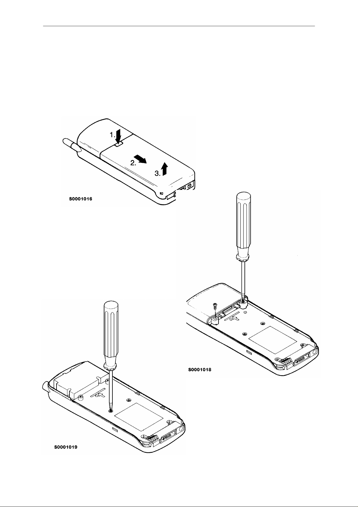
Disassembly Instructions
Remove the battery.
Disassembly & Troubleshooting
Now remove two back
cover screws and re-
move the back cover
by lifting it away.
2
1
4
3
6
Then remove six
chassis screws.
Original 11/97
5
Page 5
Page 6
NHD–4
PAMS
Disassembly & Troubleshooting
Technical Documentation
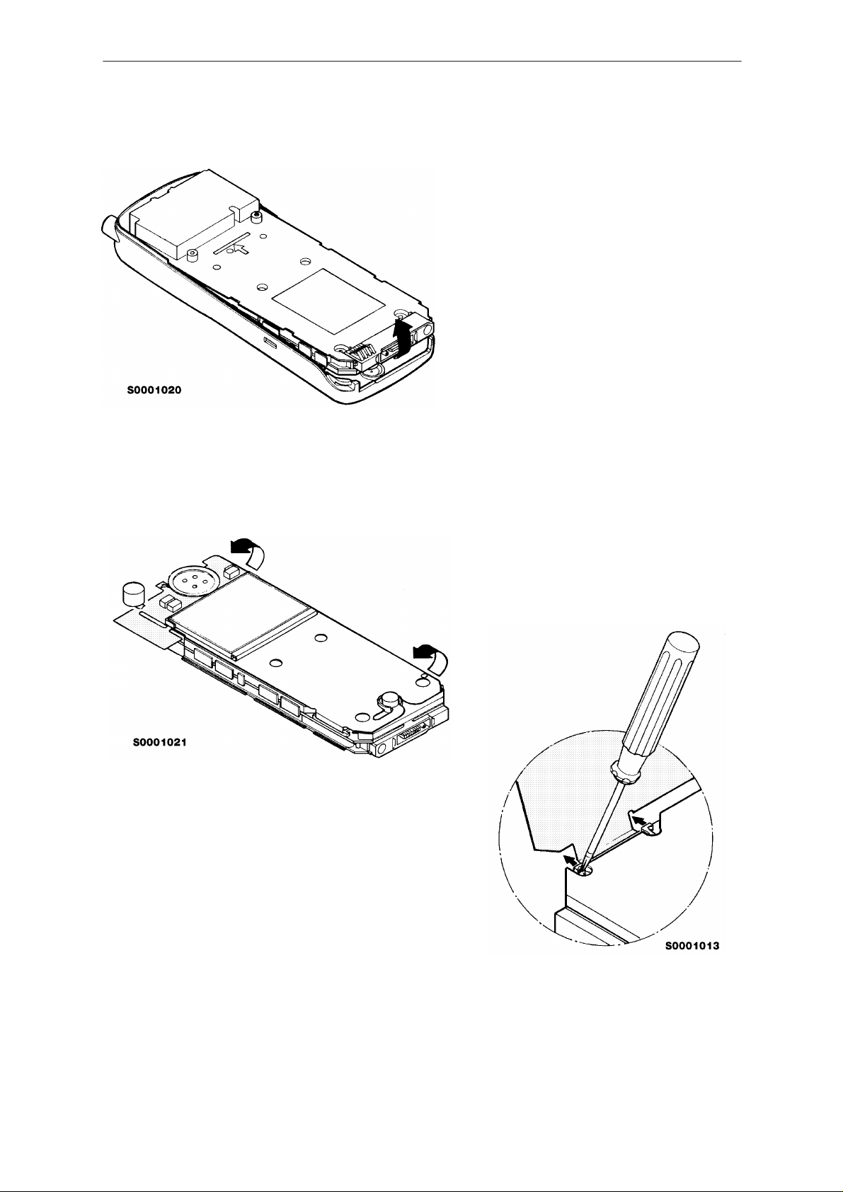
Remove the chassis by lifting.
Turn around the chassis and open
the display module a little.
Open the display module connector
by pressing both sides of connector
and slide off the display module
cable.
Page 6
Original 11/97
Page 7
PAMS
NHD–4
Technical Documentation
Turn chassis again and remove
four chassis screws.
Disassembly & Troubleshooting
1
4
3
2
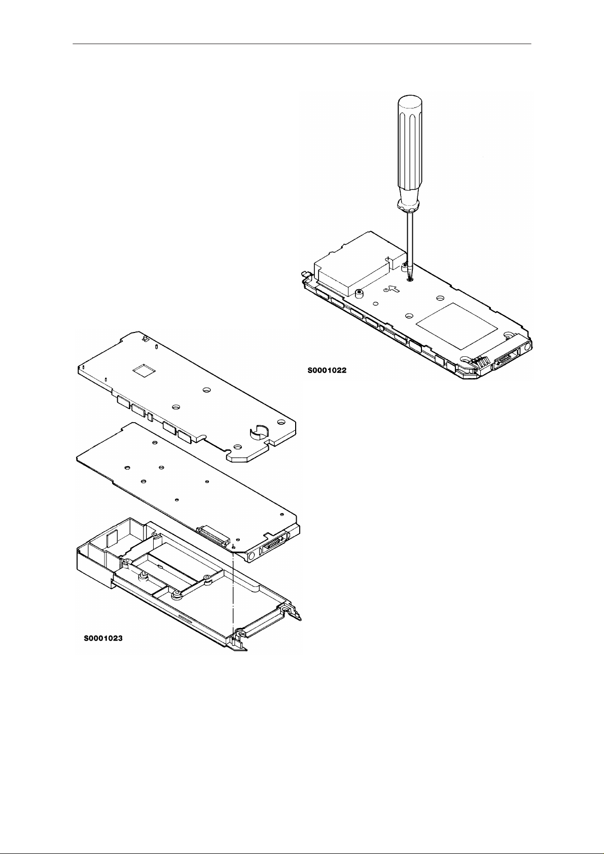
Remove the plastic shield and
throw it away (it is disposable).
Now you can separate the system module from the bottom
shield by lifting it away.
Original 11/97
Page 7
Page 8

NHD–4
PAMS
Disassembly & Troubleshooting
Baseband Troubleshooting
Overview
Baseband oriented failures are usually found out during Flash updating of
the phone, the phone should be started to minimum mode and current
consumption measured. If current consumption is within acceptable limits
and MBUS registration is OK, flash is programmed. If flash programming
fails, service software can be used to activate MCU self tests. During the
MCU self tests all the major components of the baseband are tested.
Every test returns number of the test and result ( OK / failed ).
If phone can be flashed and all self tests performed, the baseband is
mainly OK.
In case of current consumption/MBUS registration failure, the phone must
be taken to more specific measurements of voltages, clocking signals and
states of reset signals.
Technical Documentation
The flow diagrams give the overview of the blocks. The purpose is to
proceed through the flow diagram so that, if answer is YES for the asked
question, go straight to the next level, but if answer is NO, take the
sub–branch.
Required servicing equipment:
Service software
Power supply (1.0 A)
Digital multimeter
Oscilloscope
Modular cable
RS232/MBUS adapter
Soldering iron and related tools.
Current consumption failures in flash station
Current consumption can fail in three ways. Typical to all these failures is
that phone can not be programmed or tested via MBUS. The most
common failure is that phone takes normal current during startup and
after a few seconds all circuits are powered down. The reason for this
could be in power, clock or reset distribution of the phone. In cases where
phone does not take current at all or phone takes all available current the
reason could be defective PSL_+3V(N500) or bad soldering (short or
open) around PSL_+3V(N500).
Page 8
Original 11/97
Page 9

PAMS
NHD–4
Technical Documentation
Phone takes all available current
If phone takes all available current, the problem can be caused by bad
solder joints in PSL_+3V(N500), components around it and bottom
connector(X701).
Phone does not take current at all
If phone does not take current at all, check the following things:
– solder joints in PSL_+3V(N500)
– VBATT voltage should be available in pins 5 and 20 of PSL_+3V(N500),
if connections of PSL_+3V(N500) are OK and VBATT in pins 5 and 20 are
OK, change PSL_+3V(N500).
Current consumption OK during power–up, then fail
If the phone starts almost normally, but after few seconds all circuits are
powered down, the power–down, could be caused by lack of watchdog
signal from MCU(D706) to PSL_+3V(N500) . There are three major things
to be checked in this type of situation. First, check power distribution to all
baseband–main components. Then check that clocks are delivered to
CDRFI(N700), ASIC(D704), DSP(D705) and MCU(D706). If everything is
OK, check RESET status of circuitry mentioned above.
Disassembly & Troubleshooting
Checking the baseband power distribution
Before voltage measurements, power–down of PSL_+3V(N500) must be
prevented. This is done by shorting the watch–dog timing capacitor C507
with a wire soldered from one end of the capacitor to the other.
1.Check PSL_+3V(N500) output voltages pins 4, 21,16, 2, 24 and 1.
Expected value is around 3.15V. Also, check voltage in pin 12 (DETIN) to
be between 1.46V and 1.72V.
2.Check MCU(D706) supply voltage VL1(3.15V) on pins 5 and 42. Check
VREF (3.15V) voltage on MCU(D706) pin 60. Check voltages of
MCU(D706) related memory components: FLASH(D709) pins 30, 31 and
11; RAM(D700) pin 28; and EEPROM(D703) pin 7.
3.Check ASIC(D704) supply voltage VL1(3.15V) on pins 13, 22, 27, 44,
60, 65, 74, 88,103, 109, 117, 132, 146, 151, 161, and 176.
4.Check DSP(D705) supply voltage VL2(3.15V) on pins 8, 11, 36, 39, 49,
64, 76, 87 and 90. VL2(3.15V) is also fed to DSP RAM (D707) to pin 11
and 33.
5.Check CDRFI(N700) supply voltage VL3(3.15V) on pins 32, 33, 60, 62,
2, 6, 8 and 19.
6.Check supply voltages of audio CODEC(N600). VA2(3.15V) is fed to
pins 2 and 3. VL1(3.15V) is connected to pin 15.
Original 11/97
Page 9
Page 10
NHD–4
PAMS
Disassembly & Troubleshooting
Technical Documentation
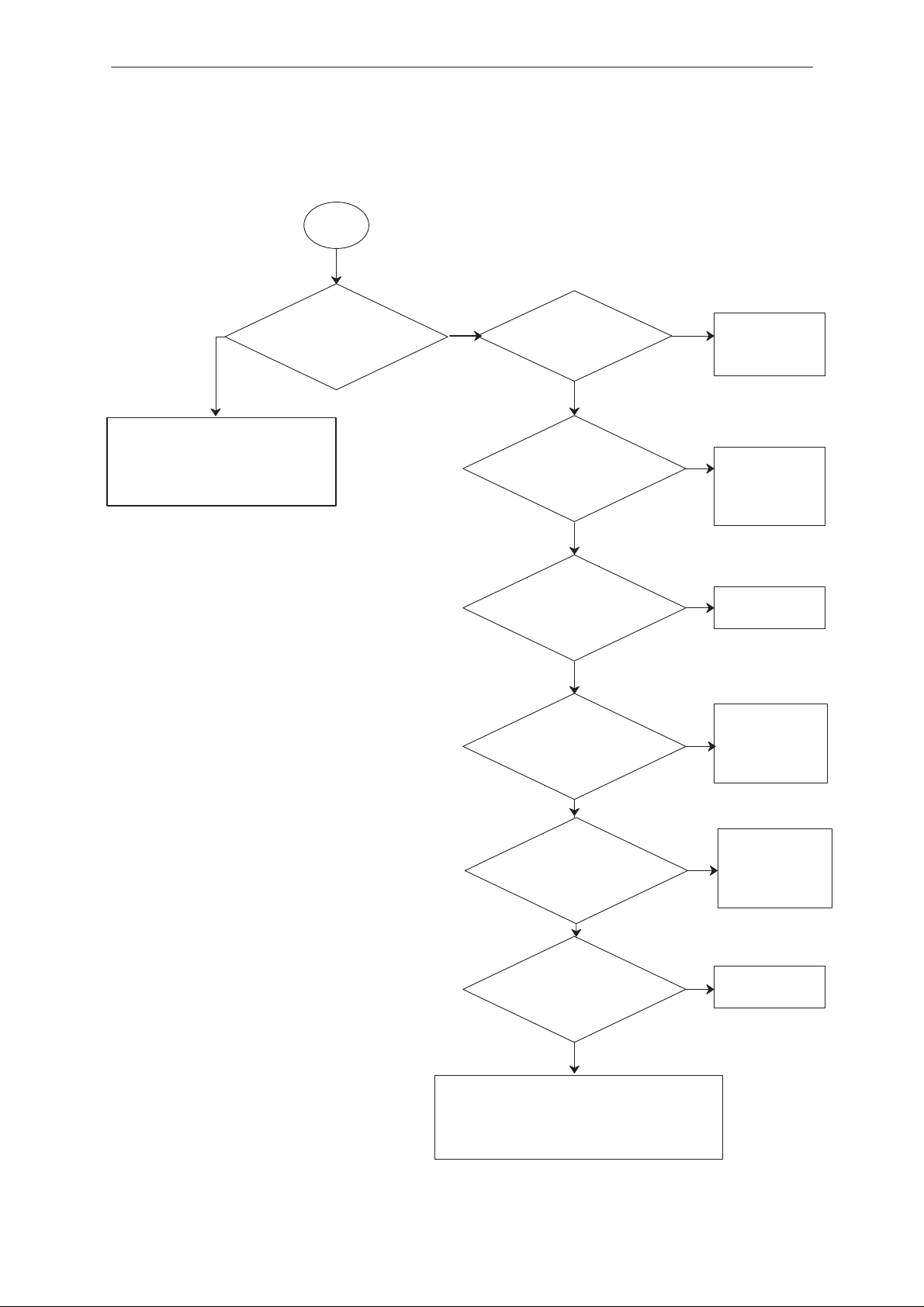
Troubleshooting Diagram; Flash Programming, part 1
FLASH programming OK
MBUS
registration
OK?
NO
YES
Does LCD
display turns
ON?
YES
NO
Check D706 pins 3,80
ASIC pins 130,86
3
Short circuits in data
data lines. data line
disconnected, VREF
disconnected
Check that pin 4 of D500
NO
is 4.75V. Also check the
control line, it should be
high (3V on Pin 1 of
Check X701
C507 OK?
YES
Power
stays on?
NO
NO
NO
N500 pin 8/XRESET
VBATT
N500 pin 5,20
?
YES
3V after power ON?
YES
display turns
YES
MBUS line X701
pin 5, Is 4.75V after
YES
Does LCD
ON?
pwr ON?
NO
D500).
R500, R503
OK?
YES
Change N500
YES
Power supp. to the logic
circuits +3V after power
ON?
NO
Change N500
D706 pin 67
+3V after power ON?
NO
YES
2
YES
Change D706
Check V703,
R728, R726,
R727, if OK
change D706
Page 10
Original 11/97
Page 11
PAMS
NHD–4
Technical Documentation
Disassembly & Troubleshooting
Troubleshooting Diagram; Flash Programming, part 2
2
NO
Check D704 and D706 for
short/open pins, if pins look
OK change D704 if problem
continues change D706
D706 pin 10
XSYS_RESET +3V after
power on?
YES
15.36MHz at
D706 pin 69
?
YES
D706 pin8/MD2
and pin9/STBY are
+3V ?
YES
NO
NO
Check clock
signal in N700
and D704
Check these
two pins for
shorts and
opens
D706 pin 43/
XPWROFF has 0V to +3V
pulses after power
ON ?
YES
D706 pin 77
/IRQ0 +3V after
power on?
YES
D706 pin 11
/NMI 0V after
power on?
YES
D706 pin 4
/XMCU_WR +3V
after pwr on?
NO
Change D706
Check D704 and
NO
D706 for shorts
and opens. If OK
change D706
Check D704 and
NO
D706 for shorts
and opens. If OK
change D706
NO
Check D706
Original 11/97
YES
Check all soldered joints
The data and address signals must have
a clear difference between low (0 V)
and high (+3V)
Page 11
Page 12
NHD–4
PAMS
Disassembly & Troubleshooting
Technical Documentation
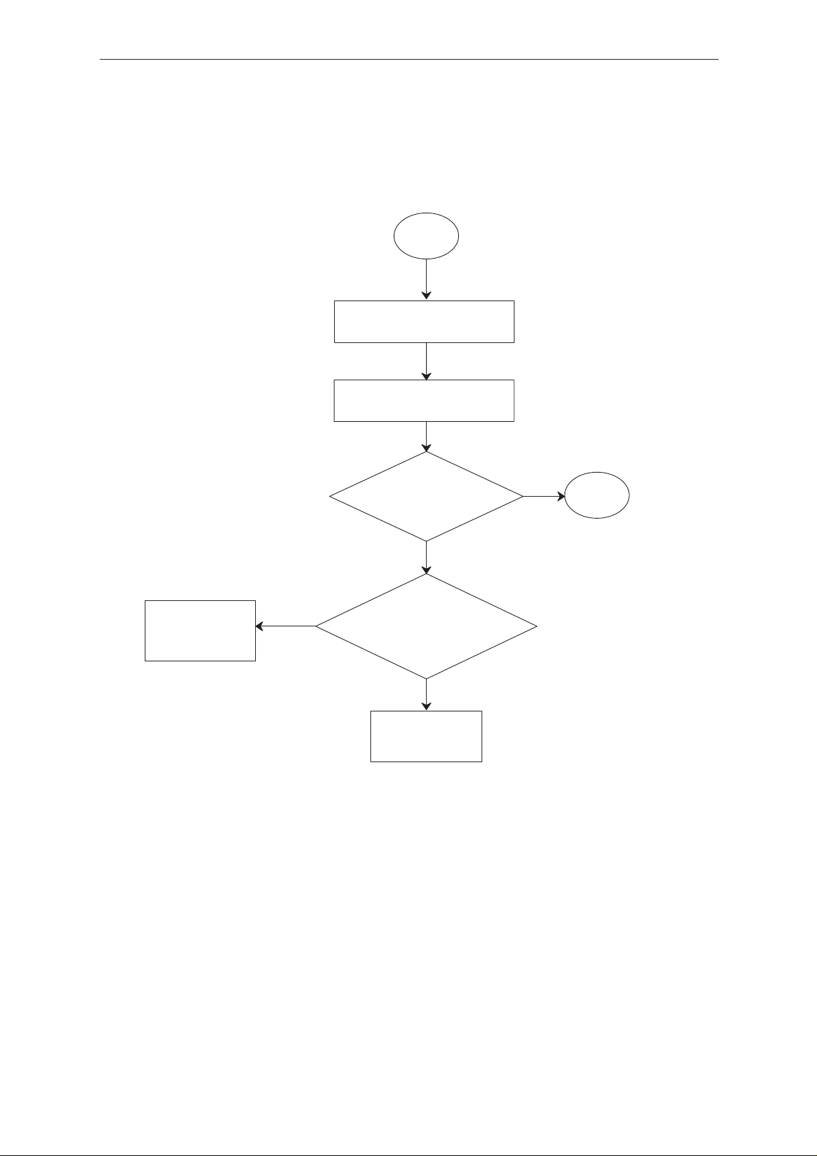
Troubleshooting Diagram; Flash Programming, part 3
3
MBUS registration OK?
YES
Does LCD display turns ON ?
YES
Check D706
and D703
interface
NO
D703 initialization
(Factory Values Set) OK?
NO
D703
pin 18,19/D0,D1
+3V to 0V during r/w
operations ?
YES
Change D703
YES
4
Page 12
Original 11/97
Page 13
PAMS
NHD–4
Technical Documentation
Disassembly & Troubleshooting
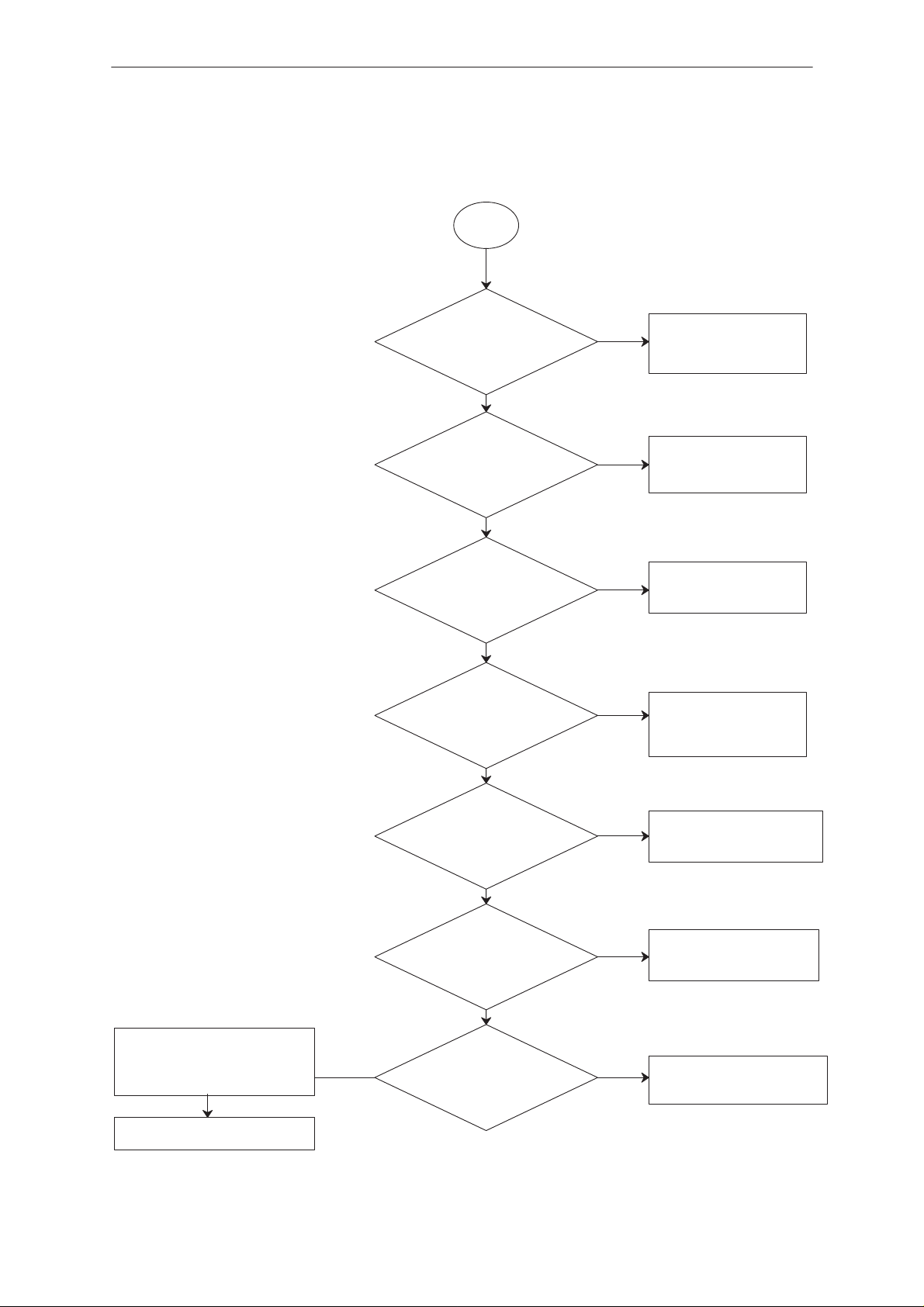
Troubleshooting Diagram; Flash Programming, part 4
4
D709
/pin 23, 39 +12V while
programming?
YES
D706
/pin 64/HOOK_RXD2
pulses during prog?
YES
NO
NO
Check X701/pin14
L700,C729,R748
R741
Check X701 pin 6
R736,R739,R764
C723
X701 pin 7
/PHFS_TXD2 pulses
during programming?
YES
D709
pin 10/RP +3V after
power ON ?
YES
D709
pin 22/CE pulses
from +3V to 0V after
power ON?
YES
D709
pin 24/OE pulses
from +3V to 0V after
power ON ?
NO
NO
NO
NO
Check D706 pin 63
R725,R735,C721
Check VCO_EN line
at the D709 pin 10 for
shorts and opens
Check XFLASH_CS
line at theD704 pin 107
Check XMCU_RD line
at the D706 pin 3
Check D709 address and
data lines for shortcircuits
or unconnected pins
OK
Change D709
Original 11/97
YES
D709
pin 9/WE pulses
from +3V to 0V after
power ON ?
NO
Check XMCU_WR line
at the D706 pin 4
Page 13
Page 14
NHD–4
PAMS
Disassembly & Troubleshooting
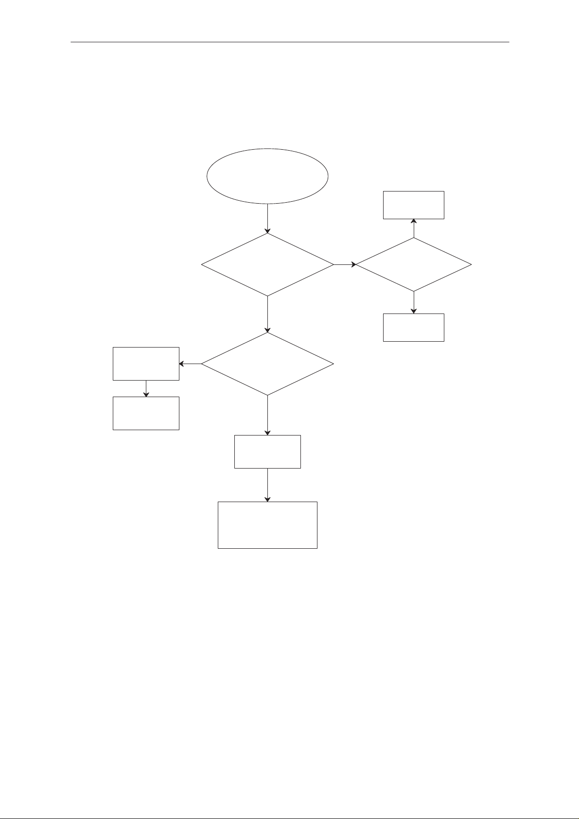
Troubleshooting Diagram; PWR Button Fault
Nothing happens when
PWR button is pressed
N500
pin 10 +3V when
VBATT is connected?
YES
NO
Technical Documentation
Check
X701
NO
N500 pins 5,20
VBATT voltage?
YES
Change
N500
Check
UI–conn. X700
Change
UI
NO
pin 10 goes low when
N500
PWR button is
pressed?
YES
R500,R503
C507 OK
Check component
around N500, if OK
change N500
Page 14
Original 11/97
Page 15
PAMS
NHD–4
Technical Documentation
Troubleshooting Diagram; Audio Fault
Audio fault
Microphone or earphone
signal missing
N600 pin 19/CODEC_FS from D704
Microphone and
earphone signal
missing?
NO
YES
N600 pin 20/CODEC_MCLK from D704
D705 pins 29,37/CODEC_FS from D704
D705 pins 27,33/CODEC_MCLK from D704
Disassembly & Troubleshooting
Microphone signal
missing?
NO
Earphone signal
missing?
YES
YES
N600 pin 25,24/MICP,MICN
N600 pin 17/PCMOUT
N600 pin 21/MICENX
corresponding pins of UI–connector
N600 pin 7,8/EARP,EARN
N600 pin 10/PCMIN
corresponding pins of UI–connector
Original 11/97
Page 15
Page 16
NHD–4
PAMS
Disassembly & Troubleshooting
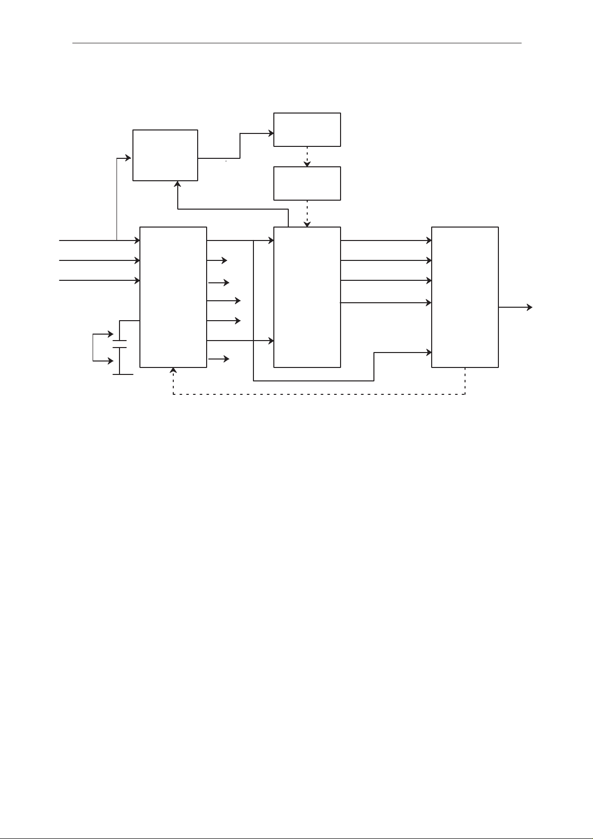
Power Up Sequence Diagram
VBAT 5.3....8V
CHRGDET
DETIN
ON
CDCONT
N201
5, 20
11
12
14
XPWROFF
C507
23
N500
9
13
VRXS 4.5V
VCO_EN
VL1 MCU_CLK (15.36MHz)
4
VL2
21
VL3
16
VA1
2
VA2
24
XRESET
82
VREF
1
VCTCXO
G300
CLK 15.36MHz
1
CDRFI N700
63
CLK 15.36MHz
128
147
104
168
ASIC MCUPSL
121
98
D704
Technical Documentation
Square circuitry
XSYS_RESET (3.15V)
MCU_INT0 (3.15V)
MCU_NMI (0V)
ON=3.15V
69
10
77
11
5,42
D706
43
66
TXD
PSL_+3V(N500)
Output voltages must stay high at least 7seconds when power is switched
on.
If no; check C507.
If it is OK; replace PSL_+3V(N500).
If the XRESET line doesn’t rise check DETIN. The voltage value at this
pin should be between 1.46V and 1.72V.
ASIC(D704)
When XRESET and CLK are supplied to the ASIC(D704) but MCUCLK or
XSYS_RESET to the MCU(D706) are not supplied; replace ASIC(D704).
MCU(D706)
If MCU_CLK and XSYS_RESET are supplied from ASIC(D704) but TXD
line (MBUS) doesn’t rise and solder joints of the MCU(D706) are good,
check that MCU_INT0 is high (3.15V) and MCU_NMI is low (0V), if that is
the case then replace MCU(D706).
XPWROFF 7s
Page 16
If TXD pin 66 of the MCU(D706) goes high but doesn’t stay there at least
7seconds.
The power of the phone can be kept ON by:
– Connecting PSL +(N500) pin 14 to the ground.
Now it is possible to use service software for troubleshooting.
Original 11/97
Page 17

PAMS
NHD–4
Technical Documentation
Disassembly & Troubleshooting
Repairing Instructions for Flash Faulty Units
1. When the phone doesn’t start (power off after 7seconds and probably no MBUS
connection) check following things:
VBATT is connected to the PSL_+3V(N500)
XRESET rises to 3.15V
VL1 is 3.15V
32KHz clock is running.
VRXS(4.5V) is connected to the VCTCXO and the crystal frequency is
15.36 MHz
XSYS_RESET signal rises to 3.15V
MCU_CLK signal is 15.36 MHz
MCU_NMI line stays low(0V)
MCU_IRQ0 line stays high(3.15V)
If all these happens, the MCU(D706) will supply power OFF pulses to the
PSL_+3V(N500) and the power will stay on.
In faulty conditions, most likely MCU_IRQ0 stays low(0V), which means
that interrupt is generated all the time.
In this case check data and address lines of ASIC(D704), MCU(D706)
and memory circuits for short circuits or unconnected pins.
2. When FLASH programming is not succeed, check following things:
System connector(X701) pins 6, 7, 14 are soldered and there are no short
circuits.
Flash programming voltage (VF=12V) is connected to the FLASH(D709)
pins 23 and 39.
The data and address lines of the FLASH(D709) are soldered.
EEPROM(D703) should be OK because of the initialization (program pa-
rameters are loaded always when program is loading the first time).
Calibrate Battery Voltage (VBATDET)= 6.0V
a) Check R505, R504
b) Check PSL_+3V(N500) pin 23
c) Check MCU(D706) pin 52
Calibrate Charge Voltage (VC)= 6.0V
a) Check R502, R501, R508
b) Check MCU(D706) pin 53
Original 11/97
Page 17
Page 18
NHD–4
PAMS
Disassembly & Troubleshooting
Technical Documentation
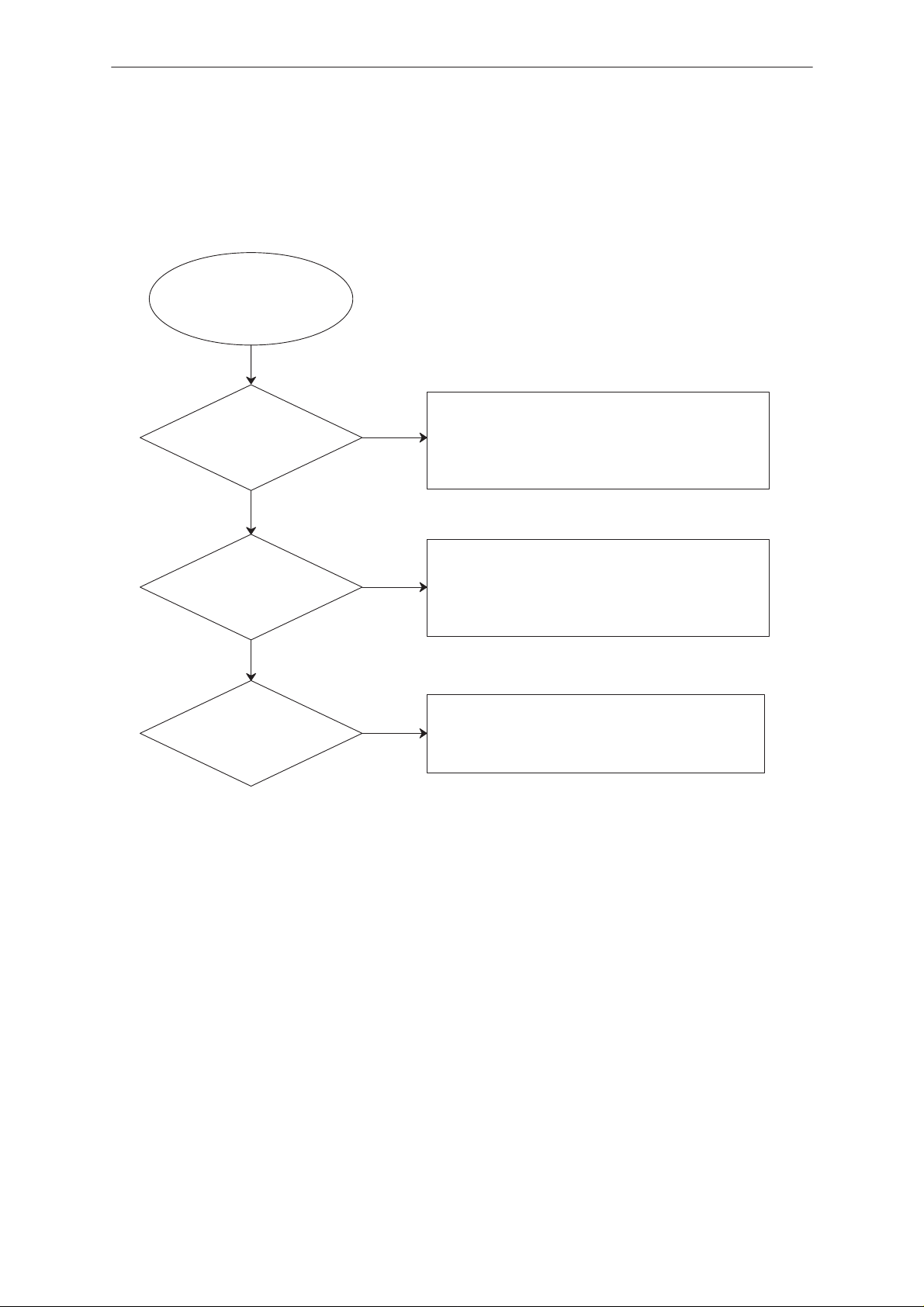
Troubleshooting Diagram; Power Up and MCU Self tests
Malfunctions
RADIO UNIT CHECK
Press power on
Current
consumption
OK?
YES
Run self tests
OK?
NO
NO
See Power Up
Malfunction
See Self Tests
Malfunction
YES
Call process
Audio check
OK
Page 18
Original 11/97
Page 19

PAMS
NHD–4
Technical Documentation
Power Up Malfunction
Basically there are two different problems that could occur while powering
up the phone. First, the current consumption is almost zero all the time.
Probably the fault is at the power circuit PSL_+3V(N500). Check all
PSL_+3V(N500) connections including VBATT line.
Second, the phone’s current consumption is normal for 7seconds and
goes to zero after that time. The reason for this is the watchdog.
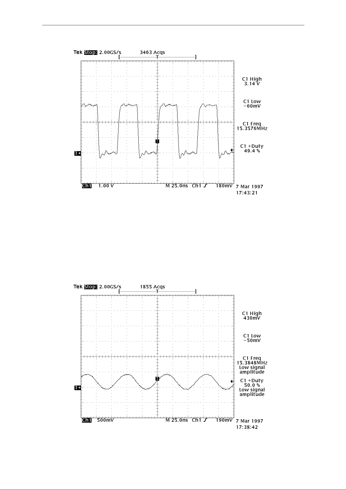
1.0 Is MCU’s clock running?
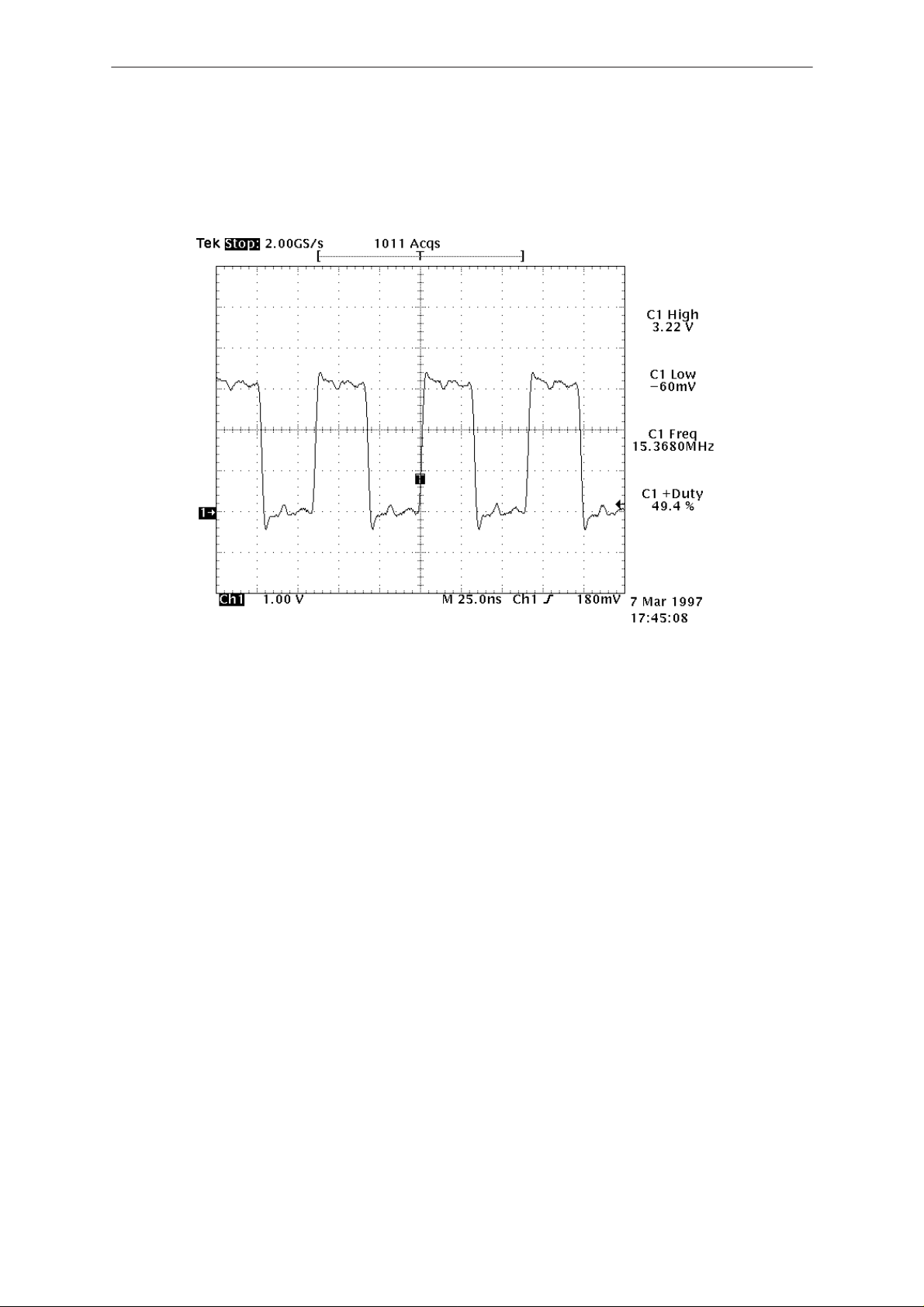
Check with oscilloscope if there is a clock signal at MCU(D706) pin 69. It
should be a square wave signal, 50% duty cycle, 3Vpp and 15.36MHz.
See Figure 1. Is the clock running?
YES! Go to 2.0 / NO! Go to 1.1
Disassembly & Troubleshooting
Figure 1
Original 11/97
1.1 Is VCTCXO running?
– Measure CDRFI(N700) pin 1. See Figure 2. Is there a
15.36MHz sine wave signal?
– YES! Go to 1.2 / NO! Go to 1.11
Page 19
Page 20
NHD–4
PAMS
Disassembly & Troubleshooting
Technical Documentation
Figure 2
1.11 Check VCO_EN is high (3.15V) CDCONT(N201) pin 23.
1.12 Check VCTCXO(G300) waveform at CDCONT(N201) pin
35 looks like Figure 3. Also check that VRXS line is 4.5Vdc at
CDCONT(N201) pin 13. If all these conditions are meet check
solder joints for shorts and opens, if they are OK replace
CDCONT(N201).
Page 20
Figure 3
Original 11/97
Page 21
PAMS
NHD–4
Technical Documentation
1.2 Check CDRFI(N700) pin 63. See Figure 4. Is there a
15.36MHz clock signal present?
– YES! Go to 1.22 / NO! GO to 1.21
Disassembly & Troubleshooting
Figure 4
1.21 Check this signal solder joints, if OK replace
CDRFI(N600).
1.22 Check connections between ASIC(D704) and MCU
(D706), especially ASIC(D704) pin 104 and MCU(D706) pin
69. If no clock is present and connection looks OK replace
ASIC(D704).
2.0 Are MCU’s supply voltages OK?
Measure MCU(D706) supply voltages from pins 5 and 42 (nominal 3.15V
±0.15 Vdc). Are supply voltages right?
V
dc
YES! Go to 3.0 / NO! Go to 2.1
2.1 Check PSL_+3V(N500) VL1(3.15V) pin 4
3.0 Is XSYS_RESET signal OK?
Check XSYS_RESET at MCU(D706) pin 10. While a high (about 3.15
V
) is ok, GO to 4.0. If zero then MCU(D706) is in reset, GO to 3.1.
dc
Original 11/97
3.1 Is XPWR_RESET signal from PSL_+3V(N500) OK?
– Check XPWR_RESET line from PSL_+3V(N500) pin 8. If it
is high GO to 3.12, if zero GO to 3.11.
Page 21
Page 22

NHD–4
PAMS
Disassembly & Troubleshooting
3.11 Check PSL_+3V pin 12. Voltage should be between 1.46V
and 1.72V. if not check R500, R503 and VBATT voltage(5.3...8
V
)
NOTICE! Measure pin 10 from the PSL_+3V(N500) with
dc
oscilloscope. That is watchdog signal coming from
MCU(D706). There should be rising edges time to time.
these are OK and still XPWR_RESET is low replace the
PSL_+3V(N500).
3.12 Check reset line for shorts and open between MCU(D706)
and ASIC(D704), and between PSL_+3V(500) and
ASIC(D704). If OK replace ASIC(D704).
4.0 Is 32KHz clock running?
Check with oscilloscope if there is a 32.768KHz clock signal at
ASIC(D704) pin 87. It should look like Figure 5.
YES! Go to 5.0 / NO! Go to 4.1
Technical Documentation
If all
Page 22
Figure 5
4.1 Check solder joints in ASIC(D704) pins 36, 37, 46, 125.
Also check B700, C744, C745, R837, R757, If they are OK replace B700. If problem persists replace ASIC(D704).
5.0 Check all supply voltages!
Measure all power supply voltage lines VL1(3.15V), VL2(3.15V),
VL3(3.15V), VA2(3.15V) and VREF(3.15V).
Are voltages right? YES! Go to 6.0. / NO! Read ahead!
If any voltage is not the right one, check corresponding transistor. VL1
(V500), VL2(V502) and VL3(V501).
Check also all major circuits supply voltages MCU(D706), ASIC(D704),
PSL_+3V(N500), DSP(D705), CDRFI(N700) and CODEC(N600).
Original 11/97
Page 23

PAMS
NHD–4
Technical Documentation
6.0 FLASH–line OK? Power up function OK!
YES! Power up function OK! / NO! Do flashing again.
This table might help to locate power pins on main circuits.
Circuit Number Pins Supply voltage signal
MCU D706 5,42 VL1
ASIC D704 13,22,27,44,60,65,74,88,103 VL1
D704 109,117,132,146,151,161,176 VL1
DSP D705 8,11,36,39,49,64,76,87,90 VL2
CDRFI N700 32,33,60,62,2,6,8,19 VL3
CODEC N600 2,3 VA2
N600 15 VL1
FLASH D709 30,31,11 VL1
RAM D700 28 VL1
EEPROM D703 7 VL1
Disassembly & Troubleshooting
Original 11/97
Page 23
Page 24

NHD–4
PAMS
Disassembly & Troubleshooting
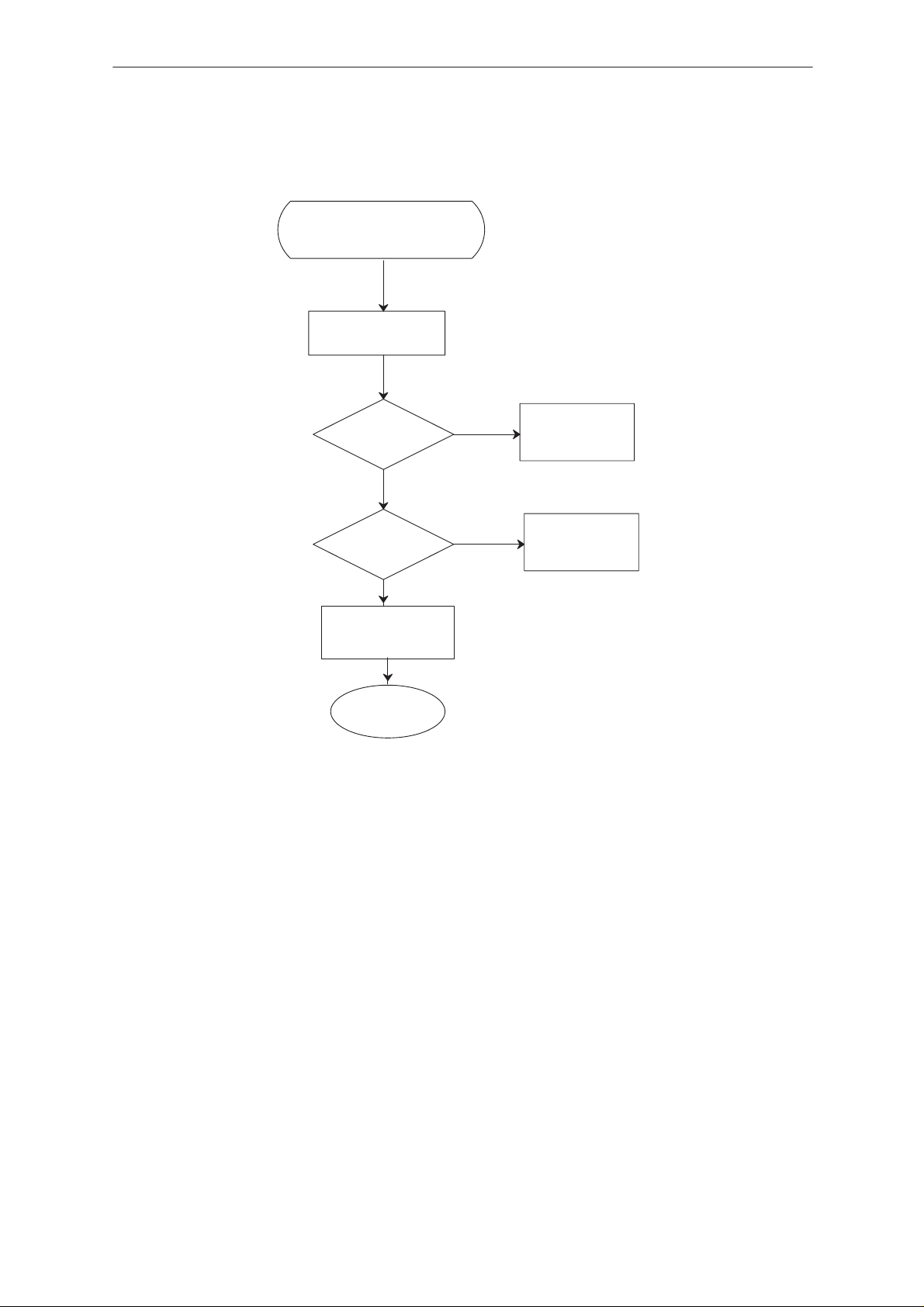
Troubleshooting Diagram; Power Up Malfunction
Start
1.11 Check
VCO_EN is 3V
1.12 Check
Vctcxo sine wave
and VRXS is
4.5V, if OK
replace CDCONT
(N201)
Check solder
joints, if OK
replace
CDRFI
(N700)
NO
1.1 VCTCXO
running OK?
YES
NO
1.2 Clock signal
at CDRFI (N700)
pin 63 ?
YES
1.22 Check connections
between D706 and D704
especially clock signals.
If they are OK replace
D704
NO
1. MCU
clock running
OK?
YES
2. MCU’s
supply voltages
OK?
YES
3. MCU
reset signal OK?
YES
NO
NO
Technical Documentation
2.1 Check PSL+(N500)
VL1–line at pin 4
3.1 Is N500
XPWR_RESET signal
OK?
YES
3.12 Check connections
between D706, D704 and
N500. If OK replace D704
NO
3.11 Check
PSL+(N500)
pins 10
and 12
if OK replace
PSL+(N500)
Page 24
Check
corresponding
component
Power up
OK!
YES
NO
4. Is 32KHz
clock running
OK ?
YES
5. All supply
voltages OK?
YES
6. FLASH line
OK?
NO
NO
4.1 Check D704 pins 36,
37,46,125. Also check
B700, C744, C745, R837.,
R757. If they are OK
replace B700. If problem
persists replace D704
Do flashing again
Original 11/97
Page 25

PAMS
NHD–4
Technical Documentation
Important Information
This section contains information that might be helpful while
troubleshooting an HD881 phone. However it is not needed to
troubleshoot power up problems.
9.8304MHz clock
This clock is ”ON” when the phone is set to CDMA non–slotted mode and
it is ”OFF” when the phone is set to AMPS mode. It is generated inside the
CDCONT(N201) from the 15.36MHz. The waveform signal coming out
from the CDCONT(N201) pin 40 should look like Figure 6.
Disassembly & Troubleshooting
Figure 6
Then this signal is fed to the CDRFI(N700) squaring circuit on pin 3 to get
the final 9.8304MHz clock signal that will go to the ASIC(D704). This clock
should look like Figure 7.
Original 11/97
Page 25
Page 26

NHD–4
PAMS
Disassembly & Troubleshooting
Technical Documentation
Figure 7
Page 26
Original 11/97
Page 27

PAMS
Á
Á
NHD–4
Technical Documentation
Transmitter Troubleshooting
Introduction
Troubleshooting the NHD–4 transmitter is very straight forward.
Operation of the transmitter circuit changes little from AMPS to CDMA
mode, only the nature of the signal transmitted is distinctly different. A
substantial amount of information regarding the health of the transmitter
can be determined with just a simple DMM. The detector voltage will
provide you a sound estimate of the output power. Collector and base
voltages will inform you if biasing is correct on the gain stages (drain and
gate for CLY–10 V113). And the various control signal had their DC
voltage characteristics detailed in the Functional Description. An RF
probe can also be used to quickly determine if a gain stage or filter is
functioning properly.
Below are a number of techniques to test the transmitter, beginning with a
means to simply turn it on. Service Software features that provide manual
transmitter controls are detailed. Node voltages RF power levels and a
chart of gains and losses are provided. Means to test the various TX
control features are explained.
Disassembly & Troubleshooting
Service Software Quick Checks
The Service Software has a number of features that allow you to quickly
test out the functionality of the transmitter in both the CDMA and AMPS
modes. The following two quick checks simply turns the transmitter on in
either of these modes.
AMPS TX Quick Checks with Service Software
From the Service Software select the AMPS Quick Checks option from the
Testing menu. A window will appear. Within this window are numerous
AMPS related controls for the phone, including a means to turn on the
AMPS transmitter. This is done by simply selecting the AMPS power level
0–2 through 7. Measure the output power using a spectrum analyzer,
power meter or RF communications test set.
AMPS TX
Power Level
БББББ
0–2
3
4
5
6
7
AMPS TX
Output Power
ÁÁÁÁ
(dBm)
27.0
23.0
18.0
14.0
10.0
8.0
Original 11/97
Page 27
Page 28

NHD–4
Á
Á
PAMS
Disassembly & Troubleshooting
CDMA TX Quick Checks with Service Software
The Service Software contains a Quick Check for the CDMA TX. From
the Test menu choose the CDMA Quick Test selection. A sub menu will
appear. Select the CDMA TX Quick Check. A window will appear
instructing you to feed the transmitter output into either a spectrum
analyzer or CDMA test box. Selecting the “TEST” soft button will turn on
the CDMA transmitter to its maximum power, approximately 24 dBm. If
not, then there is either some gain missing or a failure to provide the
appropriate input signal.
It should be noted that in CDMA operation, proper output power
measurements require that the bandwidth be taken into strict
consideration. CDMA output power readings must be performed across a
1.23 MHz band. A spectrum analyzer used for such measurements must
have the functionality to read band power. Otherwise, a CDMA signal
simply appears as an amplified noise floor, 1.23 MHz wide. For maximum
CDMA TX output power, the peak of this noise–like signal will be
approximately 10 dBm. CDMA test boxes have this capability built in.
Technical Documentation
Manual Output Power Control
The following two tests provide means to manually control the output
power of the NHD–4 transmitter in either the AMPS or CDMA modes.
AMPS TX Gain Control – Manual Control
The AMPS transmitter gain is controlled from the TXI_REF PDM. This
PDM has a manual control within the AMPS Quick Checks window of the
Service Software Test menu. With the phone in AMPS Troubleshooting
Mode the transmitter output power can be manipulated with this PDM
control. The table below details approximate PDM values, in decimal,
necessary to achieve corresponding power levels. These values will vary
from phone to phone.
AMPS TX
Output Power
БББББ
(dBm)
30
27
24
21
18
15
12
9
6
TXI_REF PDM
decimal value
ÁÁÁÁ
00
238
208
176
166
160
155
152
151
Page 28
Original 11/97
Page 29

PAMS
Á
Á
Á
Á
Á
Á
NHD–4
Technical Documentation
CDMA TX Gain Control – Manual Controls
As the name suggests, the CDMA TX Manual Gain Control mechanism of
the Service Software provides a means to manually manipulate the output
power of the CDMA transmitter. This test is convenient for testing the two
gain control functions of the CDMA transmitter, the CDAGCT IC and
Auxiliary AGC.
You can find this control within the CDMA Quick Checks selection of the
Tests menu of the Service Software. The output power is controlled by
adjusting the slide bar up and down, or manually entering numeric values
within the text edit box. Use a spectrum analyzer with a 2 MHz span to
view the transmitter output.
This test is adjusting the CloopRef register value, a value that determines
the difference between the received power into the mobile and the
transmit power out of the mobile. Artificially adjusting it, as this test does,
results in a change in the transmit power level. For this test maximum
CDMA output power, about 24 dBm, is achieved with a decimal value of
approximately 105. Minimum CDMA output power is achieved with a
decimal entry of about 25. At this level the CDMA signal will be as low as
the noise floor.
Disassembly & Troubleshooting
Detector DC Voltage Check – AMPS
Measuring the detector voltage, TXI, is great way to test transmitter output
power without actually reading the RF output power. Probing the detector
with a DMM at N202 pin 1 will provide a DC voltage that directly
corresponds to the amount of RF power sampled by the detector (V114).
This is a good means to assist in isolating transmitter faults. Whether or
not the detector voltages are valid will inform you if power losses are
occurring before or after the final PA stage (CLY–10, V113).
The following table shows typical detector output voltages for each AMPS
output power level.
AMPS
Power Level
БББББ
БББББ
0–2
3
4
5
6
7
AMPS Output Pow-
er
ББББББ
( dBm )
ББББББ
27
23
18
14
10
8
Detector Voltage
TXI
БББББ
at N202 pin 1
(V)
БББББ
0.87
1.35
1.80
1.99
2.13
2.17
Original 11/97
Page 29
Page 30

NHD–4
PAMS
Disassembly & Troubleshooting
DC Node Voltage Checks
Typical nodal voltages are listed below. The phone must be at AMPS
output power level 2 or maximum CDMA output power when measuring
node voltages. These two states can be achieved by using the AMPS or
CDMA Troubleshooting Modes.
NODE
VTXS – DC supply at C144
VTXT – DC supply at R120
V114 – Detector output ( TXI ) at N202 pin 1
V114 – Detector supply at R127 ( VTXS )
V113 – CLY–10 PA supply at C160 ( VRFT )
V113 – CLY–10 PA gate at R138 ( VGG )
V112 – 3rd Gain stage collector at C157
V112 – 3rd Gain stage base at C164
V112 – 3rd Gain stage supply at R117
V110 – 2nd Gain stage collector at C154
V110 – 2nd Gain stage base at R129
V111 – 1st & 2nd Gain stages supply at C108
V111 – 1st Gain stage collector at C146
V111 – 1st Gain stage base at R128
V106 – AT–109 atten. – supply at C129 ( VTXS )
V106 – AT–109 atten. – control at C109 ( VC )
N100 – Bias to the CDAGCT IC at C133
RFE2 at V107 emitter
VRFT– Battery voltage at C142
VNEG – Gate Volt. Delay at R111
TX_PUNC – Puncture Control at V102
TX_IREF – Control current reference at C115
TX_ICT – Control current at C100
Technical Documentation
CDMA
VDC
4.40
5.30
1.20
4.40
6.20
–2.70
6.00
0.70
6.3
2.68
0.72
4.70
3.85
0.75
4.40
3.50
3.90
0.00
6.80 *
–4.12
3.12
3.60
3.60
AMPS
VDC
4.40
5.30
1.10
4.40
6.20
–2.30
6.00
0.70
6.20
2.67
0.72
4.70
3.83
0.75
4.40
4.35
3.90
3.10
6.80 *
–4.05
3.12
3.50
3.50
Note This is the Battery voltage. It directly reflects the power supply voltage to the
phone. It will only be 6.8 V when the DC supply to the phone is 6.8 V.
Note: The position of the probe’s GND pin is critical to obtain correct readings. The GND
pin MUST be touching the GND plane immediately next to the point being measured!!
RF Node Power Levels
A high impedance passive RF probe may be used with a spectrum
analyzer to obtain the RF node power levels along the transmitter chain.
The author recommends a passive probe with a 500 ohm tip. The
following levels are based on a transmitter output at AMPS power level 7.
Maintain a 1.0 MHz span on the spectrum analyzer. A CDMA test box
with spectrum analyzer capabilities will do.
The RF power levels published below were found with a passive probe
with the 500 ohm tip. The blank column is reserved for values the user
will obtain with their own probe.
Page 30
Original 11/97
Page 31
PAMS
Á
Á
Á
Á
Á
Á
Á
Á
Á
Á
Á
Á
Á
Á
Á
Á
Á
Á
Á
Á
NHD–4
Technical Documentation
Node
БББББББББ
БББББББББ
БББББББББ
N100 – CDAGCT pin 8
N100 – CDAGCT pin 2
N100 – CDAGCT pin 31
N100 – CDAGCT pin 32
V106 – AT–109 pin 3 (input)
V106 – AT–109 pin 7 (output)
Z100 – TX SAW pin 2 (input)
Z100 – TX SAW pin 5 (output)
V111 – 1st Gain stage – base
V111 – 1st Gain stage – collector
V110 – 2nd Gain stage – base
V110 – 2nd Gain stage – collec-
БББББББББ
tor
Z101 – TX SAW pin 5
Z101 – TX SAW pin 2
V112 – 3rd Gain stage – base
V112 – 3rd Gain stage – collec-
БББББББББ
tor
V113 – CLY–10 PA gate
V113 – CLY–10 PA drain
V710 – Isolator pin 2 (input)
Z102 – Duplexor TX port
Z102 – Duplexor ANT port
Disassembly & Troubleshooting
Frequency
ББББББ
(MHz)
ББББББ
ББББББ
180.00
926.52
836.52
836.52
836.52
836.52
836.52
836.52
836.52
836.52
836.52
836.52
ББББББ
836.52
836.52
836.52
836.52
ББББББ
836.52
836.52
836.52
836.52
836.52
Power Lvl
ÁÁÁ
HP10020A
500 ohm tip
ÁÁÁ
(dBm)
ÁÁÁ
–22.5
–30.4
–35.0
–36.6
–36.8
–49.0
–45.0
–45.0
–40.0
–28.0
–22.8
–8.5
ÁÁÁ
–14.6
–12.8
–26.5
1.7
ÁÁÁ
–13.3
6.7
5.7
6.0
6.0
Power Lvl
ÁÁÁÁ
(your own)
(dBm)
ÁÁÁÁ
ÁÁÁÁ
ÁÁÁÁ
ÁÁÁÁ
Original 11/97
Page 31
Page 32

NHD–4
Á
Á
Á
Á
Á
Á
Á
Á
Á
Á
PAMS
Disassembly & Troubleshooting
Testing CDMA TX Gain Limiting
To test the CDMA TX Gain Limiting control perform the following steps:
1. Place the phone in the CDMA Troubleshooting Mode.
2. With an oscilloscope probe the LIM_ADJ line at C807.
3. Adjust the gain of the CDMA transmitter using the CDMA TX manual
gain control mechanism found in the Service Software.
4. The LIM_ADJ line will remain at about 3.2 VDC until the TX output
power reaches its limit, approximately 24 dBm. At this point the LIM_ADJ
line will toggle continuously, appearing as a square wave 3.2 Vpp with an
approximate frequency of 400 Hz.
Testing Dynamic TXB
To test the Dynamic TXB functionality, perform the following steps:
1. Place the phone in the CDMA Troubleshooting Mode.
2. Use the Service Software CDMA TX manual gain controls to achieve
10 dBm CDMA TX output power.
Technical Documentation
3 .Read the total current draw of the phone. It should be approximately
530 mA.
4. Increase the CDMA TX output power to 23 dBm. The current draw
should rise to approximately 690 mA.
Note the difference is about 150 mA, which is the difference between the two current
biasing levels.
CDMA TX
БББББББ
БББББББ
Current Draw
ÁÁÁ
10 dBm
(mA)
ÁÁÁ
530
ÁÁÁÁ
ÁÁÁÁ
Testing CDAGCT IC (N100) Gain Control
To test the gain control abilities of the CDAGCT IC (N100) do the
following:
1. Place the phone in the CDMA Troubleshooting Mode
2. Observe the TX output with a spectrum analyzer or CDMA test set. Be
sure to read bandpower over a 1.23 MHz band.
CDMA TX
23 dBm
(mA)
690
AMPS Power
ÁÁÁÁ
Level 7
(mA)
ÁÁÁÁ
400
AMPS Power
ÁÁÁÁ
Level 2
(mA)
ÁÁÁÁ
610
Page 32
3. Use the CDMA TX manual gain control found in the Service Software
to adjust the output power from its minimum (noise floor) to 15 dBm.
4. Observe the TX_Gain voltage at C213 and the TX_ICT current as a
voltage drop across R116. The table below details approximate values
that should be read.
Original 11/97
Page 33
PAMS
Á
Á
Á
Á
Á
Á
Á
Á
Á
Á
Á
Á
Á
Á
Á
Á
NHD–4
Technical Documentation
CDMA TX Output
RF Signal Level
БББББ
(dBm)
БББББ
15
10
–5
–20
–35
Testing Auxiliary AGC
To test the gain control abilities of the Auxiliary AGC feature, perform the
following steps:
1. Place the phone in the CDMA Troubleshooting Mode
2. Observe the TX output with a spectrum analyzer or CDMA test set. Be
sure to read bandpower over a 1.23 MHz band.
3. Use the CDMA TX manual gain control found in the Service Software to
adjust the output power of the phone from 15 dBm to 23 dBm.
TX_GAIN Voltage
at C213
БББББ
БББББ
(V)
1.78
1.80
1.87
1.93
2.00
Disassembly & Troubleshooting
TX_ICT Control
Current
БББББ
БББББ
(mA)
0.700
0.560
0.298
0.171
0.093
TX_ICT
(as voltage drop
БББББ
across R116)
БББББ
(mV)
70.0
56.0
29.8
17.1
9.3
4. Observe the VC voltage at C109 and the AGC_REF PDM voltage at
C716. The table below details approximate values that should be read.
CDMA TX
БББББ
Output Power
БББББ
(dBm)
23
21
19
17
15
Hints and Suggestions
The 3rd stage (V112) is sensitive to shorts of the DC bias line.
Accidentally shorting the collector to ground always blows the 5.6 ohm
bias resistor (R117) but doesn’t harm the transistor.
AGC_REF PDM
БББББ
(decimal value)
БББББ
0
34
60
79
85
AGC_REF PDM
БББББ
voltage at C716
БББББ
(V)
0.798
0.583
0.456
0.367
0.333
БББББ
БББББ
VC
at C109
(V)
3.28
2.81
2.53
2.33
2.26
Original 11/97
Page 33
Page 34

NHD–4
PAMS
Disassembly & Troubleshooting
AMPS Receiver Troubleshooting
Introduction
Troubleshooting the NHD–4 AMPS receiver isn’t unlike troubleshooting
the AMPS receiver on any other Nokia phone. In fact, NHD–4 uses the
same FM receiver IC as many other Nokia phones. So long as the
NHD–4 phone is in an AMPS RX mode, this receiver will be on. The
following tests detail ways to make the AMPS receiver operational and
test its functionality.
Tests and Quick Checks
The Service Software software package contains a quick test for the
AMPS receiver. When selected, the software prompts you to send a
modulated carrier into the phone at a –65 dBm signal level. Hitting the
”Test” soft key prompts the software to read the RSSI voltage level that
the CDRFI IC has A/D converted into a digital signature. If the digital
value falls within the range which a –65 dBm signal should, it is a good
bet that the AMPS receiver is working properly. There is still a chance
that the demodulated baseband ANARX signal (the audio) is corrupt, but
you do know the rest of the AMPS receiver is functional.
Technical Documentation
If the RSSI values are less
RX sensitivity problem. Most likely a component or solder joint along the
AMPS RX receiver path has failed. The possibility exists that the error is
in the baseband A/D conversion. To ensure that the error is in the RF it is
recommended that the remaining tests below be performed until the error
is uncovered.
If the RSSI values are greater
energy above the stated input level is entering the RX path. Check the
level of the signal generator used for the test. It may be sourcing more
RF power than was requested by the test. Ensure that cable losses have
been properly accounted for.
than the ranges stated, than there is an AMPS
than the ranges stated than additional RF
Setting Up the AMPS Receiver Test
To troubleshoot the AMPS receiver first remove the shields. Apply power
and service cables to the phone and turn it on. Initiate the AMPS
Troubleshooting Mode from Service Software. Then feed a –65 dBm
881.52 MHz signal modulated with 8 kHz FM and 1 kHz audio into the RF
port of the phone via the bottom connector. A stand alone RF signal
generator should do the trick, or a CDMA test box with this functionality.
Do not forget to account for the signal loss between the signal generator
and the phone.
Page 34
Original 11/97
Page 35

PAMS
NHD–4
Technical Documentation
RSSI Check
The voltage on the ungrounded end of C13 directly represents the RSSI of
the phone. Checking this voltage will provide another quick indication of
the health of the AMPS RX module. With the –65 dBm modulated signal
mentioned above this voltage should be approximately 2.00 V.
The possibility exists that the AMPS RX is working fine with a –65 dBm
input, but has lost sensitivity and fails at lower input powers. You may
wish to perform this test at higher or lower input signal levels. The
following table details the RSSI voltage vs. input signal levels. Keep in
mind that there will be variations in the voltage levels from phone to
phone, but these are good approximations.
–45
–50
–55
–60
–65
–70
–75
–80
–85
–90
–95
–100
–105
Disassembly & Troubleshooting
2.32
2.31
2.26
2.16
2.00
1.89
1.78
1.65
1.54
1.41
1.26
1.17
1.07
If the RSSI DC voltages are significantly less than the ranges stated then
there is an AMPS RX sensitivity problem. A total AMPS RX failure would
yield about 1.00 V for this test for most input RF power levels. Most likely
a component or solder joint along the AMPS RX receiver path has failed.
Continue the DC Voltage Quick Checks to help determine if any of the
devices aren’t biased correctly.
If the RSSI values are significantly greater than the ranges stated then
additional RF energy above the stated input level is entering the RX path.
Check the level of the signal generator used for the test and ensure that
cable losses have been properly accounted for. Also check for any
undesired oscillations.
Original 11/97
Page 35
Page 36

NHD–4
PAMS
Disassembly & Troubleshooting
DC Voltage Checks
Check the following DC voltages with the –65 dBm modulated signal still
fed into the phone and the Service Software AMPS Troubleshooting Mode
initiated.
•The bias voltage on the AMPS RX IC (D1), pin 4 should be
approximately 4.40 V.
If not, first ensure that the phone is in the AMPS Troubleshooting Mode. Check the
VRXA supply voltage at C219, or CDCONT (N201), pin 42. If fault is found with this
DC supply then refer to the AGC Troubleshooting Manual to determine if there is a
problem with the CDCONT voltage regulators.
•Check the 1st IF gain stage V9:–
The voltage on the collector, pin 1 should be approximately 3.30 V.
If not, confirm that the phone is in the AMPS Troubleshooting Mode. Inspect V9, R30
and R31. Ensure that VRXAM is approximately 4.15 V at R31
Technical Documentation
The voltage on the base, pin 3 should be approximately .97 V.
If not, confirm that the phone is in the AMPS Troubleshooting Mode. Inspect V9, V4,
L13, L11, R4, R5, R13, R14, and R15. Ensure VRXM is at about 4.15 V at R13, and
VRXAM is about 4.15 V.
The voltage on the emitter, pins 2 and 4 should be approximately 0.25 V.
If not, confirm that the phone is in the AMPS Troubleshooting Mode. Inspect V9,
L14, R25, and R28.
•Check the LNA, V12:–
The voltage on the collector should be approximately 3.70 V.
If not, confirm that the phone is in the AMPS Troubleshooting Mode. Ensure VRXM
is at about 4.15 V at R833. Inspect V11, V12, L20, R33, R34, R38, and R833.
The voltage on the base should be .82 V.
If not, confirm that the phone is in the AMPS Troubleshooting Mode. Ensure VRXM
is at about 4.15 V at R833. Inspect V11, V12, L21, L22, R33, R35, and R833.
•Check the control voltages on the RF Gain Switches N701 and N702.
Pin 1 on both should be approximately 3.80 V.
Page 36
If not, confirm that the phone is in the AMPS Troubleshooting Mode. Ensure VRXM
is at about 4.15 V at R832. Inspect N701, N702, V1, V708, R775, R777, R779,
R781, R783, R803, R830, R831, and R832.
•Check the SWAGC line at R830. It should be logic level low,
approximately .0 V.
If not, confirm that the phone is in the AMPS Troubleshooting Mode. Ensure VRXM
is at about 4.15 V at R832. Inspect V708, R765 and R830. Ohm out line from R765
to the ASIC N704 pin 94.
Original 11/97
Page 37

PAMS
Á
Á
NHD–4
Technical Documentation
•Check the RX_CAL line at R783, It should be logic level high, near 2.75 V.
If not, confirm that the phone is in the AMPS Troubleshooting Mode. Ensure VRXM
is at about 4.15 V at R832. Inspect V1, V708, R6, R765, R783, and R785. Ohm out
the RX_CAL line from pin 114 of the ASIC N704 to R785.
Chart of AMPS RX DC Node Voltages
The following chart summarizes the node voltages of the AMPS RX when
the phone is in the AMPS RX/TX Mode with a 881.52 MHz signal input of
–65 dBm, modulated with 8 kHz FM, 1 kHz audio.
ББББББББББББ
D1 – AMPS RX IC, pin 4
V9 – collector of 1st IF amp, pin 1
V9 – base of 1st IF amp, pin 3
V9 – emitter of 1st IF amp, pins 2, 4
V12 – collector of LNA
V12 – base of LNA
RF Gain Switches N701 and N702, pin 1
RF Gain Switches N701 and N702, pin 8
SWAGC line at R830
RX_CAL line at R783
Node
Disassembly & Troubleshooting
БББББББ
Voltage
(V)
4.40
3.30
0.97
1.12
3.70
0.82
3.80
0.00
0.00
2.75
Demodulation Test
If you have an oscilloscope available you may use it to do a visual check
on the demodulated 1 kHz tone on the ANARX+DA line. Again feed in the
modulated –75 dBm, 881.52 MHz, 8 kHz FM, 1 kHz audio RF signal into
the receiver and initiate the AMPS Troubleshooting Mode from Service
Software. Use a standard scope probe at C1 to look at the 1 kHz tone. It
should appear as a clean sine wave of approximately 380mVpp. Step
down the input RF power. At about –90 dBm the sine wave will begin to
become a bit fuzzy. At –105 dBm the waveform will be fuzzy, but still
distinguishable.
If not, confirm that the phone is in the AMPS Troubleshooting Mode.
Ensure the RF signal is modulated correctly and of the requested signal
level. Inspect R2, C1 and C10.
RF Node Power Checks – AMPS Mode
A high impedance passive RF probe may be used with a spectrum
analyzer to obtain the RF nodal power levels along the receiver chain.
The following levels assume a –65 dBm, 881.52 MHz, unmodulated tone
input into the receiver. Maintain a 1.0 MHz span on the spectrum
analyzer. A CDMA test box with spectrum analyzer capabilities will do.
The RF power levels published below were found a passive probe with the
500 ohm tip. The blank column is reserved for values the user will obtain
with their own probe.
Original 11/97
Page 37
Page 38

NHD–4
Á
Á
Á
Á
Á
Á
Á
Á
Á
ББББББ
Á
Á
Á
Á
ББББББ
ББББББ
ББББББ
ББББББ
ББББББ
ББББББ
ББББББ
ББББББ
ББББББ
ББББББ
ББББББ
ББББББ
ББББББ
ББББББ
ББББББ
ББББББ
ББББББ
PAMS
Disassembly & Troubleshooting
Node
БББББББББ
БББББББББ
БББББББББ
44.545 MHz osc. at D1, pin 2
AMPS RX IC D1 pin 16
SAW Z3 pin 3
SAW Z3 pin 6
Diode V10 pin 3/L15/R29/R30
1st IF Amp V9 collector, pin 1
1st IF Amp V9 base, pin 3
Mixer T1 pin 4 – IF
Mixer T1 pin 8 – LO
Mixer T1 pin 5 – RF
RF Switch N701 pin 7 – output
RF Switch N701 pin 5 – input
LNA V12 collector
LNA V 12 base
RF Switch N702 pin 7 – output
RF Switch N702 pin 5 – input
Duplexor Z102, RX In pin
Duplexor Z102, ANT pin
Coax W400 Antenna input
Coax W400 Connector input
Frequency
ÁÁÁÁ
(MHz)
ÁÁÁÁ
ÁÁÁÁ
44.545
45
45
45
45
45
45
45
926.52
881.52
881.52
881.52
881.52
881.52
881.52
881.52
881.52
881.52
881.52
881.52
Technical Documentation
Power Lvl
БББББ
HP10020A
500 ohm tip
БББББ
(dBm)
БББББ
–10
–62
–61.5
–57.5
–90
–90
–105
–80
–19
–75
–75.5
–75.5
–68
–90
–85.5
–85.5
–92
–89
–87
–88
Power Lvl
ÁÁÁÁ
(your own)
(dBm)
ÁÁÁÁ
ÁÁÁÁ
Page 38
Original 11/97
Page 39

PAMS
NHD–4
Technical Documentation
CDMA Receiver Troubleshooting
Introduction
Troubleshooting the CDMA receiver of the phone is unique, but not
complicated. The following tests detail numerous ways that the CDMA
receiver functionality can be verified, all using standard test equipment.
No special CDMA signal generators or measurement equipment are
necessary to verify the CDMA receiver.
CDMA RX Quick Test with Service Software
The Service Software software package contains a quick test for the
CDMA receiver. When selected, the software prompts you to send a CW
carrier into the phone at a –65, –85, and –105 dBm signal levels, one after
the other. Hitting the ”Test” soft key prompts the software to read the
received signal level that the phone perceives digitally. A numeric value
called the RxDAC (RX D/A converter) is generated within the CDMA ASIC
to represent the signal level received. If this number falls within the range
of values listed in the Service Software window coinciding with the
respective input signal level, the CDMA RX is operating properly. For
example, for a –65 dBm input signal should provide an RxDAC value
between 480 and 520.
Disassembly & Troubleshooting
Note: The results of this test will only fall into the ranges stated when the RX_OFFSET
is properly tuned. With this parameter improperly tuned the resultant values will be
slightly different, but still near the stated ranges, provided that the CDMA RX module is
functional.
Set Up CDMA RX Test
To troubleshoot the CDMA receiver first remove the shields. Apply power
and service cables to the phone and turn it on. Initiate the CDMA RX
Troubleshooting Mode from Service Software. Then feed a –65 dBm
881.62 MHz unmodulated CW carrier into the phone via the RF connector
at the bottom of the phone. An unmodulated –65 dBm carrier at channel
387 will also work. A stand alone RF signal generator should do the trick,
as will a CDMA test box with this functionality. Do not forget to account for
the signal loss between the signal generator and the phone.
RX Gain Control Test
A great test to check the health of the CDMA receiver is to monitor the
gain control current to the CDAGCR IC. As the CDMA signal strength
received by the phone drops, this current increases. Naturally it is difficult
and time consuming to break the circuit and position an ammeter in the
phone to read this current. A quick way to do so is to simply read the
voltage drop across resistor R16. Position one test lead of a volt meter on
either side of this resistor and vary the RF input power at 881.62 MHz,
unmodulated CW.
The voltage drop across this resistor should resemble the values in the
table that follows. Be sure to also check the voltage drop across R17, the
RX_IREF signal. This drop should be approximately 360 mV.
Original 11/97
Page 39
Page 40

NHD–4
Á
Á
Á
Á
PAMS
Disassembly & Troubleshooting
RF Input Power
БББББББ
881.62 MHz CW
БББББББ
(dBm)
–45
–50
–55
–60
–65
–70
–75
–80
–85
–90
–95
–100
–105
DC Voltage Checks
Check the following DC voltages with the –65 dBm 881.62 MHz CW signal
still fed into the phone and the Service Software CDMA Troubleshooting
Mode initiated.
Voltage Drop
БББББББ
Across R16
(RX_ICT)
БББББББ
(mV)
11
14
17
21
25
30
37
45
56
68
83
99
113
Technical Documentation
•The bias voltage on the BFILCT2 IC (N2), pin 4 should be approx 3.10 V.
If not, first ensure that the phone is in the CDMA Troubleshooting Mode. Check the
VBBFIL supply voltage at the collector of V203, or CDCONT (N201), pin 15, or C223.
It should be approximately 3.15 V.
•The bias voltage on the BFILCT2 IC (N2), pin 8 should be approx 3.05 V
If not, first ensure that the phone is in the CDMA Troubleshooting Mode. Check the
VRXD_R supply voltage at pin 4 of V206, or CDCONT (N201), pin 15, or C223. It
should be approximately 4.50 V.
•The bias voltage on the CDAGCR IC (N1), pin 13 should be approx 4.40 V.
If not, first ensure that the phone is in the CDMA Troubleshooting Mode. Check the
VRXD_R supply voltage at pin 4 of V206, or CDCONT (N201), pin 15, or C223. It
should be approximately 4.50 V.
•Measure the voltage drop across R17 at the RX_IREF line, (one probe on
either side of this resistor). The voltage drop should be approx 330 mV.
If not, first ensure that the phone is in the CDMA Troubleshooting Mode. Ensure that
the –75 dBm 881. 62 MHz CW signal is fed into the receiver. Perform the DC Voltage checks on that module to determine if there is a problem with the AGC circuitry.
Page 40
Original 11/97
Page 41

PAMS
NHD–4
Technical Documentation
•Check the voltage drop across R16 at the RX_ICT line, placing one probe
on either side of this resistor. The voltage drop should be approx 37 mV.
If not, first ensure that the phone is in the CDMA Troubleshooting Mode. Ensure that
the –75 dBm 881. 62 MHz CW signal is fed into the receiver. If fault is found then
continue with the remaining receiver DC Voltage checks. After doing so there is still
no problem, refer to the AGC Troubleshooting Manual. Perform the DC Voltage
checks on that module to determine if there is a problem with the AGC circuitry.
•Check the CDMA IF LNA V7 and V8
The voltage on the collector of V7, pin 1 should be approximately 1.38 V.
The voltage on the base of V7, pin 3 should be approximately 1.33 V.
If not, confirm that the phone is in the CDMA Troubleshooting Mode. Inspect V8, V7,
L5, R19, R20. Ensure that VRXDM is approximately 4.50 V at R21.
The voltage on the emitter of V7, pin 2 should be approximately .60 V.
If not, confirm that the phone is in the CDMA Troubleshooting Mode. Inspect V7, and
L6.
Disassembly & Troubleshooting
•Check the 1st IF gain stage V9
The voltage on the collector, pin 1 should be approximately 3.50 V.
If not, confirm that the phone is in the CDMA Troubleshooting Mode. Inspect V10,
V9, R22, R23, Z3. Ensure that VRXDM is approximately 4.50 V at R23
The voltage on the base, pin 3 should be approximately 1.85 V.
If not, confirm that the phone is in the CDMA Troubleshooting Mode. Inspect V9, V4,
L13, L11, R4, R5, R13, R14, R15, and R24. Ensure VRXDM is about 4.50 V at R21.
See that VRXM is at about 4.40 V at R13, and VRXAM is about 1.15 V at R14
The voltage on the emitter, pins 2 and 4 should be approximately 1.12 V.
If not, confirm that the phone is in the CDMA Troubleshooting Mode. Inspect V9,
L14, R25, and R28.
•Check the LNA, V12
The voltage on the collector should be approximately 3.90 V
If not, confirm that the phone is in the CDMA Troubleshooting Mode. Ensure VRXM
is at about 4.40 V at R833. Inspect V11, V12, L20, R33, R34, R38, and R833.
The voltage on the base should be 1.0 V
•Check the control voltages on the RF Gain Switches N701 and N702.
Pin 1 on both should be approximately 3.80 V.
Original 11/97
If not, confirm that the phone is in the CDMA Troubleshooting Mode. Ensure VRXM
is at about 4.40 V at R833. Inspect V11, V12, L21, L22, R33, R35, and R833.
If not, confirm that the phone is in the CDMA Troubleshooting Mode. Ensure VRXM
is at about 4.40 V at R832. Inspect N701, N702, V1, V708, R775, R777, R779,
R781, R783, R803, R830, R831, and R832.
Page 41
Page 42

NHD–4
PAMS
Disassembly & Troubleshooting
•Check the SWAGC line at R830, should be logic level low, approx .0 V.
If not, confirm that the phone is in the CDMA Troubleshooting Mode. Ensure VRXM
is at about 4.40 V at R832. Inspect V708, R765 and R830. Ohm out line from R765
to the ASIC N704 pin 94.
•Check the RX_CAL line at R783. It should be logic level high, near 2.75 V.
If not, confirm that the phone is in the CDMA Troubleshooting Mode. Ensure VRXM
is at about 4.40 V at R832. Inspect V1, V708, R6, R765, R783, and R785. Ohm out
the RX_CAL line from pin 114 of the ASIC N704 to R785.
Chart of CDMA RX DC Node Voltages
The following chart summarizes the node voltages of the CDMA RX when
the phone is in the CDMA RX/TX Mode with a 881.62 MHz signal input of
–65 dBm, CW.
Node
BFILCT2 IC (N2), pin 4
BFILCT2 IC (N2), pin 8
CDAGCR IC (N1), pin 13
R17 – voltage drop across this resistor
R16 – voltage drop across this resistor
V7 – collector of CDMA IF LNA, pin 1
V7 – base of CDMA IF LNA, pin 3
V7 – emitter of CDMA IF LNA, pins 2, 4
V9 – collector of 1st IF amp, pin 1
V9 – base of 1st IF amp, pin 3
V9 – emitter of 1st IF amp, pins 2, 4
V12 – collector of LNA
V12 – base of LNA
RF Gain Switches N701 and N702. Pin 1
RF Gain Switches N701 and N702. Pin 8
SWAGC line at R830
RX_CAL line at R783
Technical Documentation
Voltage
(V)
3.10
3.05
4.40
0.33
0.037
1.33
1.38
0.60
3.50
1.85
1.12
3.90
1.00
3.80
0.00
0.00
2.75
Baseband Demodulation Check
If you have an oscilloscope available you may use it to do a visual check
on the demodulated baseband CDMA I or Q signal . With the phone
tuned to channel 384, feed a –75 dBm, 881.62 MHz unmodulated CW RF
signal into the receiver. Initiate the CDMA Troubleshooting Mode from
Service Software. Use a standard scope probe at C58, the RX_I signal.
It should appear as a fuzzy sine wave of approximately 190 mVpp. This
frequency will be approximately 100 kHz.
Page 42
Original 11/97
Page 43
PAMS
Á
Á
Á
Á
Á
Á
Á
Á
Á
Á
Á
Á
NHD–4
Technical Documentation
RF Node Powers – CDMA RX Mode
A high impedance passive RF probe may be used with a spectrum
analyzer to obtain the RF nodal power levels along the receiver chain.
The following levels assume the above probe and a –65 dBm, 881.52
MHz, unmodulated tone input into the receiver. Maintain a 1.0 MHz span
on the spectrum analyzer. A CDMA test box with spectrum analyzer
capabilities will do.
The RF power levels published below were found with a passive probe
with the 500 ohm tip. The blank column is reserved for values the user
will obtain with their own probe.
БББББББББ
БББББББББ
БББББББББ
CDAGCR IC N1 Pin 19
CDAGCR IC N1 Pin 8
CDMA SAW Output L6/L7/C63
Diode Switch V10 pin 4/L8/L9
1st IF Amp V9 collector, pin 1
1st IF Amp base, pin 3
Mixer T1 pin 4 – IF
Mixer T1 pin 8 – LO
Mixer T1 pin 5 – RF
RF Switch N701 pin 7 – output
RF Switch N701 pin 5 – input
LNA V12 collector
LNA V12 base
RF Switch N702 pin 7 – output
RF Switch N702 pin 5 – input
Duplexor Z102, RX In pin
Duplexor Z102, ANT pin
Coax W400 – Antenna input
Coax W400 – Connector input
Node
ББББББ
ББББББ
ББББББ
Frequency
MHz)
180
45
45
45
45
45
45
926.52
881.52
881.52
881.52
881.52
881.52
881.52
881.52
881.52
881.52
881.52
881.52
Disassembly & Troubleshooting
Power Lvl
ÁÁÁ
HP10020A
ÁÁÁ
500 ohm tip
(dBm)
ÁÁÁ
–24
–61
–88
–57
–57
–80
–80
–19
–75
–75.5
–75.5
–68
–90
–85.5
–85.5
–92
–89
–87
–88
Power Lvl
ÁÁÁÁ
(your own)
(dBm)
ÁÁÁÁ
ÁÁÁÁ
Original 11/97
Page 43
Page 44

NHD–4
PAMS
Disassembly & Troubleshooting
Hints and Suggestions
AMPS
•It is important to NOT adjust the tunable inductor L17. Doing so will
NOT assist in troubleshooting a faulty receiver, it will only make
things worse. This device is tuned by its manufacturer to the proper
inductance.
•While in AMPS Troubleshooting Mode, probe the 455 kHz ceramic filter
Z4. A noise pedastle approximatly 20 kHz wide will be visible about 10
dBm above the noise floor.
CDMA
•To determine in the CDAGCR IC (N1) quadrature demodulator is
functioning, connect both the RX_I and RX_Q to CH1 and CH2 of
oscilloscope. Put the scope in X–Y mode. A Lissajous pattern of a circle
should be displayed. Changing the received signal power should not
cause the size of the circle to change.
Technical Documentation
Page 44
Original 11/97
Page 45

PAMS
NHD–4
Technical Documentation
Disassembly & Troubleshooting
Synthesizer Troubleshooting
Introduction
Troubleshooting the synthesizer is difficult because the oscillations that it
produces cannot be measured at the output of the phone. The RF signals
it generates are routed to various portions of the phone. Assuming the
receiver and transmitter are functional, indirect means of determining the
health of the synthesizer can be used. Both the transmitter and receiver
depend on the synthesizers to operate. If one of the two synthesizers is
not working it is most certain that a problem will show up in either the
transmitter, receiver, or both. The Service Software RF quick checks are
great tools for initial testing. Beyond that there are a few quick DC
voltages that can be used to quickly assess the health of the phone. If all
else fails, RF node power levels can be read.
Quick Check with Service Software – Transmitter Approach
The fastest way to determine if both synthesizers are working is to turn on
the AMPS transmitter. This can be done from Service Software from the
AMPS/Baseband test menu. The unmodulated transmit signal can then
be viewed with a spectrum analyzer or CDMA test box. This test requires
that the AMPS transmitter be functional. If the transmitter is faulty the
receiver may also be used as a means to test the synthesizer.
To set up this test, connect the RF output of the phone to a spectrum
analyzer or CDMA test box using the bottom connector. If the CDMA test
box is used it is best to make use of the spectrum analyzer function if the
box used has one. If not, the AMPS TX test functions will work. Configure
the analyzer as such:
Center Frequency: 836.52 MHz (Channel 384)
Span: 20 MHz
Ref Level: 30 dBm
Turn on the AMPS transmitter from Service Software, setting the power
level to the lowest setting, level 7. Tune to channel 384. Initiating the
AMPS Troubleshooting mode also turns on the AMPS transmitter to
channel 384. Look at the AMPS transmit signal on the spectrum analyzer.
• If the signal is a strong (greater than –10 dBm) CW carrier locked to
836.52 MHz then both synthesizers are working properly. Change the
span of the analyzer to 100 kHz and ensure that the carrier is on
frequency to within 100 Hz.
• If a signal comes up but is slightly off frequency then the reference clock,
the VCTCXO (G300) is mistuned. Proceed to the section titled Testing
and Troubleshooting for Frequency Error.
Original 11/97
Page 45
Page 46

NHD–4
PAMS
Disassembly & Troubleshooting
Technical Documentation
• If the signal comes up, but is very much off frequency (more than a few
kHz) or is drifting around then the one or both of the PLLs is not locked.
Proceed to the section titled Testing and Troubleshooting for Synthesizer
Lock Error.
• If no signal is seen then it is possible that the transmitter is not working.
If the noise floor rose when you initiated the test, then it is likely that the
transmitter is working, but it has no signal to amplify. This would indicated
a faulty synthesizer. To rule out synthesizer error, proceed to the next
Service Software synthesizer test, the Receiver Approach. Performing the
DC Voltage Checks would also be advised.
Quick Check with Service Software – Receiver Approach
Another way to determine if both synthesizers are working is to test the
AMPS and CDMA receiver with a signal fed in. This can be done from
Service Software. Perform the CDMA RX RF Quick Test followed by the
AMPS RX RF Quick Test. These tests are found in the Service Software
Test menu.
• If the phone passes the CDMA RX RF Quick Test then both synthesizers
are working
• If the phone fails the CDMA RX RF Quick Test, but passes the AMPS RX
RF Quick Test, then the 180 MHz VHF synthesizer has failed, assuming
both the AMPS and CDMA receivers work. Proceed to the DC Voltage
Checks, VHF Synthesizer portion
• If the phone fails both RX RF Quick Tests then proceed to the DC
Voltage checks section.
DC Voltage Checks – AMPS Troubleshooting Mode
Put the phone into AMPS Troubleshooting Mode. This will turn both of the
synthesizers on. The following details the node voltages for the VCTCXO,
PLL IC, VHF and UHF portions of the synthesizer. Note that these node
voltages will change slightly when the phone is operating in CDMA mode.
VCTCXO (G300)
• Check the bias on pin 4. It should be near 3.60 V.
Page 46
If not, check R325, C303, and C334. Check VRXS at C207 near the CDCONT IC.
It should be approximately 4.40 V
Original 11/97
Page 47

PAMS
NHD–4
Technical Documentation
• Check the tune voltage on pin 1. It should be between 1.50 and 2.50 V.
If not, check R302, R301, and C302. Check the RX_SLOPE and AFC PDM lines.
Manually adjust them with the PDM controls within Service Software. Read the
RX_SLOPE PDM voltage at R700 and read the AFC PDM voltage at R701. While
tuned to channel 384 the RX_SLOPE PDM should be about 3.00 V. For channel 440
it should be 0.0 V. The AFC PDM will vary between 0.0 V and 3.00 V, generally near
the midrange of 1.50 V.
PLL IC (N301)
• Check the biasing on the PLL IC (N301). Pins 4 and 5 should have
approximately 3.15 V on them. Pin 18 should have about 4.40 V. Check
pin 19, AON, it should have about 2.80 V.
If not, check VRXS at C207 near the CDCONT IC. It should be approximately 4.40
V. Check the pin 14, Iset, for 1.25 V. Check VRX90 at C205 or R310. It should also
be approximately 4.40 V. Check R331, R307, R308, R310, R311, R807, R810 and
C337.
VHF Synthesizer
Disassembly & Troubleshooting
• Check the tune voltage at the cathode of V301. It should be stable at a
single voltage between 1.50 and 3.5 V.
If not, check to see that the 180 MHz oscillation is feeding back into the PLL IC at pin
15. Continue with the following two checks. Ensure that the varactor diode, V301 is
in the circuit correctly.
• Check the biasing of the buffer amp, V303.
The collector should be biased with 4.30 V.
The base should be biased with 3.30 V.
The emitter should be biased with 2.60 V.
If not, check VRX90 at R806 or at C205 near the CDCONT IC. It should be approximately 4.40 V. Inspect L303, R316, R318, R322, R323, R324, and R806. Also in-
spect C319, C321, C322, C323, C324, C328, C329, C330, C332, C333, and C340.
• Check the biasing on the oscillator transistor, V302.
The collector should be biased with 2.60 V.
The base should be biased with 2.30 V.
The emitter should be biased with 1.73 V.
• Check the biasing on the UHF VCO, G301. There should be
approximately 4.25 V at pin B.
Original 11/97
If not, check VRX90 at R806 or at C205 near the CDCONT IC. It should be approximately 4.40 V. Inspect L303, R316, R318, R322, R323, R324, and R806. Also in-
spect C319, C321, C322, C323, C324, C328, C329, C330, C332, C333, and C340.
4.3.2.4 UHF Synthesizer
If not, check R808. Check to see that VRXS is 4.40 V at C207.
Page 47
Page 48

NHD–4
Á
Á
Á
Á
PAMS
Disassembly & Troubleshooting
Technical Documentation
• Check the tune voltage at pin C. It should fall in the range of 1.5 to 3.5 V.
If not, check the PLL IC. Ensure that the RF feedback is correct into the PLL at pin 6.
• The RX_LO gain stage N704, pin 3 should be about 3.40 V.
If not, check R803 and see that VRX is 4.40 V at C206.
• The TX_LO gain stage N705, pin 3 should be about 2.70 V
If not, check R809 and R815. Ensure that VTXT is approximately 4.40 V at R809 or
C212.
Chart of Synth DC Node Voltages – AMPS Troubleshooting Mode
ББББББББББББ
Node
ББББББББББББ
G300 – VCTCXO bias, pin4
G300 – VCTCXO Tune voltage, pin 1
N301 – PLL IC bias, pins 4, 5
N301 – PLL IC bias, pin 18
N301 – PLL IC bias, pin 19
V301 – V aractor diode – 180 MHz tune voltage
V303 – VHF Buffer Amp – Collector
V303 – VHF Buffer Amp – Base
V303 – VHF Buffer Amp – Emitter
V302 – VHF Oscillator – Collector
V302 – VHF Oscillator – Base
V302 – VHF Oscillator – Emitter
G301 – UHF VCO bias, pin B
N704 – UHF RX_LO gain stage
N705 – UHF TX_LO gain stage
Voltage
ÁÁÁÁ
(approx)
ÁÁÁÁ
(V)
3.60
1.50 – 3.50
3.15
4.15
2.80
1.50 – 3.50
4.30
3.30
2.60
2.60
2.30
1.73
4.00
3.40
2.70
RF Node Power Levels
A high impedance passive RF probe may be used with a spectrum
analyzer to obtain the RF nodal power levels for the synthesizer circuit.
The following levels assume the above probe. The phone was also
operating in the AMPS Troubleshooting Mode via Service Software. The
blank column is reserved for values the user will obtain with his or her own
probe.
Page 48
Original 11/97
Page 49

PAMS
Á
Á
Á
Á
Á
Á
Á
Á
Á
Á
Á
Á
NHD–4
Technical Documentation
Node
БББББББББ
БББББББББ
БББББББББ
G300 – VCTCXO, pin 1
V303 – VHF Buffer Amp – Collector
V303 – VHF Buffer Amp – Emitter
V302 – VHF Oscillator – Collector
G301 – UHF VCO, pin P
N704 – UHF RX_LO gain stage
N705 – UHF TX_LO gain stage
Hints and Suggestions
• If no spectrum analyzer is available, a lot can be learned about the
health of a PLL by checking the control voltage tuning the VCO. If the
PLL is locked, this control, or tune voltage will fall between 1.5 and 3.5 V
DC. If the control voltage is near 0.0 or 4.4 V, the loop is most likely
unlocked.
• Probing the cathode of the varactor diode, V301 may unlock the VHF
loop.
Disassembly & Troubleshooting
Frequency
ББББББ
(MHz)
ББББББ
ББББББ
15.36
180
180
180
926.52
926.52
926.52
Power Lvl
ÁÁÁ
HP10020A
500 ohm tip
ÁÁÁ
(dBm)
ÁÁÁ
–15.0
–24.0
–30.0
–30.0
–30.0
–20.0
–40.0
Power Lvl
ÁÁÁÁ
(your own)
(dBm)
ÁÁÁÁ
ÁÁÁÁ
•Modulation cannot be seen on the anode of the varactor when using an
oscilloscope. The level is two low. Instead, measure it at R317/C341
node.
• To check to see that the PLL IC (N300) is programmed by the CDSB
ASIC (D704), probe the CLK, DATA and RX_LE lines with an oscilloscope.
Monitor the oscilloscope when the channel is changed. Use the Service
Software test functions to change the channel. When the channel is
changed the PLL IC is reprogrammed. The RX_LE line will provide 5
evenly spaced pulses. The CLK signal will be a square wave, 0.0 to 3.0 V,
and the DATA line will show a stream of pulses, with no discernible
pattern.
• To check the functionality of a VCO, apply an external DC supply to the
control voltage pin, like the C pin of G301. The output frequency of the
VCO will change when the control voltage is varied.
AGC Troubleshooting
Introduction
Detailed below are a number of tests designed to demonstrate the
functionality of the features and systems described above in the
Functional Description. All make use of the control abilities of the Service
Software, all located in the Testing menu of the software package. AMPS
feature testing is mainly performed from the AMPS/Baseband test suite.
CDMA feature testing makes use of a menu of CDMA system controls.
The two most useful features of the later group are the CDMA TX Manual
Gain controls and the CDMA RX Manual Gain controls. The PDM controls
are also used extensively throughout the testing procedures.
Original 11/97
Page 49
Page 50

NHD–4
PAMS
Disassembly & Troubleshooting
DC Supply Checks
The voltage supplies used to bias the RF module is detailed below. The
following table details the voltage of each supply when the phone is in
either AMPS or CDMA mode. Shaded boxes indicate that a supply is
active.
• AMPS RX/TX mode can be achieved by initiating the AMPS
Troubleshooting Mode from the Services Software.
• CDMA RX/TX mode can be achieved by initiating the CDMA
Troubleshooting Mode from the Services Software.
VBBFIL VNEG VRX VRXA VRXD VRXD_R VRXS VRX90 VTX VTXS
Measurement
point
AMPS RX/TX
CDMA RX/TX
C224 N200
pin 5
~ 0.0 –4.10 4.45 4.45 1.65 ~ 0.0 4.45 4.45 5.30 4.45
3.15 –4.10 4.45 1.20 4.45 4.50 4.45 4.45 5.35 4.45
C206 C219 C218 N706
CDMA TX Gain Limiting Test
To test the CDMA TX Gain Limiting control, perform the following steps:
Technical Documentation
C207 C205 C212 C200
pin 4
3. Place the phone in the CDMA Troubleshooting Mode.
4. With an oscilloscope probe the LIM_ADJ line at C807.
5. Adjust the gain of the CDMA transmitter to maximum output
power using the CDMA TX manual gain control mechanism found in the
Service Software.
6. The LIM_ADJ line will remain at about 3.2 VDC until the TX
output power reaches its limit, approximately 24 dBm. At this point the
LIM_ADJ line should toggle continuously, appearing as a square wave 3.2
Vpp with an approximate frequency of 400 Hz.
Dynamic TXB Test
To test the Dynamic TXB functionality, perform the following steps:
2. Place the phone in the CDMA Troubleshooting Mode.
3. Use the Service Software CDMA TX manual gain controls to
achieve 10 dBm CDMA TX output power.
4. Read the total current draw of the phone. It should be
approximately 530 mA.
5. Increase the CDMA TX output power to 23 dBm. The current
draw should rise to approximately 690 mA.
Page 50
Note that the difference is about 150 mA, which is the difference between
the two current biasing levels.
CDMA TX
10 dBm
(mA)
2180 Current Draw 530 690 400 610
CDMA TX
23 dBm
(mA)
AMPS Power
Level 7
(mA)
AMPS Power
Level 2
(mA)
Original 11/97
Page 51

PAMS
NHD–4
Technical Documentation
CDAGCT IC (N100) Gain Control Test
To test the gain control abilities of the CDAGCT IC (N100) perform the
following steps:
5. Place the phone in the CDMA Troubleshooting Mode
6. Observe the TX output with a spectrum analyzer or CDMA test
set. Be sure to read bandpower over a 1.23 MHz band.
7. Use the CDMA TX manual gain control found in the Service
Software to adjust the output power from its minimum (noise floor) to 15
dBm.
8. Observe the TX_Gain voltage at C226 and the TX_ICT current
as a voltage drop across R116. The table below details approximate
values that should be read.
CDMA TX Output
RF Signal Level
(dBm)
15 1.78 0.700 70.0
10 1.80 0.560 56.0
–5 1.87 0.298 29.8
–20 1.93 0.171 17.1
–35 2.00 0.093 9.3
TX_GAIN +
TX_OFFSET
Voltage
at C226
(V)
Disassembly & Troubleshooting
TX_ICT Control
Current
(mA)
TX_ICT
(as voltage drop
across R116)
(mV)
Auxiliary AGC Test
To test the gain control abilities of the Auxiliary AGC feature, perform the
following steps:
1. Place the phone in the CDMA Troubleshooting Mode
2. Observe the TX output with a spectrum analyzer or CDMA test
set. Be sure to read bandpower over a 1.23 MHz band.
3. Use the CDMA TX manual gain control found in the Service
Software to adjust the output power of the phone from 15 dBm to 23 dBm.
4. Observe the VC voltage at C109 and the AGC_REF PDM
voltage at C716. The table below details approximate values that should
be read.
CDMA TX
Output Power
(dBm)
23 0 0.798 3.28
21 34 0.583 2.81
19 60 0.456 2.53
17 79 0.367 2.33
15 85 0.333 2.26
AGC_REF PDM
(decimal value)
AGC_REF PDM
voltage at C716
(V)
VC
at C109
(V)
Original 11/97
Page 51
Page 52
NHD–4
PAMS
Disassembly & Troubleshooting
For CDMA TX operation above the switchpoint, the TX_ICT current will be
at its maximum, approximately 1.0 mA. There should be approximately
100 mV of voltage drop across R116.
For more information on the Auxiliary AGC control feature, consult section
3.4.3.2 of this document.
CDMA RX Gain Control Test
To test the gain control abilities of the CDAGCR IC (N1) do the following:
3. Place the phone in the CDMA Troubleshooting Mode
4. Use the CDMA RX manual gain control found in the Service
Software to adjust the CDMA receiver gain.
5. Verify the RX_IREF current signal as the voltage drop across
R17. The voltage drop should be approximately 350 mV.
6. Observe the RX_Gain voltage at C213 and the RX_ICT current
as a voltage drop across R16. The table below details approximate
values that should be read.
Technical Documentation
CDMA RX RF Signal
Level
(dBm)
–25 2.06 0.020 7
–45 2.00 0.033 11
–65 1.91 0.073 24
–85 1.82 0.158 52
–105 1.73 0.278 92
AMPS TX Gain Control Test
The AMPS transmitter gain is controlled from the TXI_REF PDM. This
PDM has a manual control within the AMPS Quick Checks window of the
Service Software Test menu. With the phone in AMPS Troubleshooting
Mode the transmitter output power can be manipulated with this PDM
control. The table below details approximate PDM values, in decimal,
necessary to achieve corresponding power levels. These values will vary
from phone to phone.
AMPS TX
Output Power (dBm)
30 00
27 238
24 208
21 176
18 166
15 160
12 155
9 152
6 151
RX_GAIN Voltage
at C213
(V)
RX_ICT Control
Current
(mA)
TXI_REF PDM
decimal value
RX_ICT
(as voltage drop
across R16)
(mV)
Page 52
Original 11/97
Page 53

PAMS
NHD–4
Technical Documentation
Note the PDM decimal values are not linearly related. Therefore the maximum value of
255 roles over to the minimum value of 0 at the midpoint of the scale. This explains the
significant difference between the PDM decimal values of 27 dBm to 30 dBm.
CDMA AGC Loop Test
This procedure tests the ability of the CDMA transmitter output power to
track the CDMA receiver input power. This requires a configuration of the
test equipment that allows the ability to view the transmitter output power
while varying the input receive power. However, for this test it is not so
important to know the absolute output power of transmitter, but rather to
see the change in output as a function of the change in input. Configure
either of these devices as such:
Spectrum Analyzer (Measures output of TX)
Frequency: 836.52 MHz
Disassembly & Troubleshooting
Span: 2 MHz
Amplitude: 30 dB
Signal Generator (Injects signal into RX)
Frequency: 881.62 MHz
Modulation: None (CW signal)
Perform the test as such:
2. Calibrate any cable loss between the phone and the test box.
3. Set the input signal amplitude to –65 dBm
4. Read the bandpower of the output CDMA signal. It should be
approximately –8 dBm.
5. Decrease the input signal amplitude to –85 dBm.
6. Read the bandpower of the output CDMA signal. It should be
approximately 12 dBm, a 20 dB shift from the previous state.
Note: This test assumes that the phone is properly tuned. If it is not, the
20 dB change in input signal strength may not correspond to a 20 dB
change in TX output. If bandpower cannot be read, then simply look at
the 1.23 MHz wide CDMA signal with the spectrum analyzer. The peak
will increase about 20 dB with a 20 dB decrease in the receiver input.
Another method to perform this test would be to make use of a spectrum
analyzer and signal generator as separates. In this case a circulator used
to isolate the input and output signals of the phone from the signal
generator and spectrum analyzer respectively. Be sure to calibrate out
the cable and circulator losses.
Original 11/97
Page 53
Page 54

NHD–4
PAMS
Disassembly & Troubleshooting
[This page intentionally left blank]
Technical Documentation
Page 54
Original 11/97
 Loading...