

Page 1

Programme’s After Market Services
Technical Documentation
SER VICE
MANUAL
[NMP Part No. 0275396]
NHP–4 SERIES
CELLULAR
PHONES
Issue 1 04/99
MOBILE PHONES
Copyright 1999. Nokia Mobile Phones. All Rights Reserved.
Page 2

Programme’s After Market Services
Technical Documentation
AMENDMENT RECORD SHEET
Amendment
Number
Date Inserted By Comments
Issue 1 04/99
Copyright 1999. Nokia Mobile Phones. All Rights Reserved.
Page 3

Programme’s After Market Services
Technical Documentation
Chapter 1
Foreword
Issue 1 04/99
Page 1–1
Page 4

Programme’s After Market Services
Technical Documentation
CHAPTER 1– FOREWORD
CONTENTS
Introduction 1–3. . . . . . . . . . . . . . . . . . . . . . . . . . . . . . . . . . . . . . . . . . . . . . . . . . . . . .
Service Manual Structure 1–3. . . . . . . . . . . . . . . . . . . . . . . . . . . . . . . . . . . . . . .
Company Policy 1–4. . . . . . . . . . . . . . . . . . . . . . . . . . . . . . . . . . . . . . . . . . . . . . .
Warnings and Cautions 1–5. . . . . . . . . . . . . . . . . . . . . . . . . . . . . . . . . . . . . . . . . . .
Warnings: 1–5. . . . . . . . . . . . . . . . . . . . . . . . . . . . . . . . . . . . . . . . . . . . . . . . . . . .
Cautions: 1–5. . . . . . . . . . . . . . . . . . . . . . . . . . . . . . . . . . . . . . . . . . . . . . . . . . . . .
Page No
Page 1–2
Issue 1 04/99
Page 5

Programme’s After Market Services
Technical Documentation
Introduction
Service Manual Structure
The service manual is structured as follows:–
The ’core’ service manual
Chapter 1: Foreword
Chapter 2: General Information
Chapter 3 System Overview
Chapter 4: System Module
Chapter 5: UIF Modules
The core section of the service manual describes those areas of the
NHP–4 series handportable phone which are common to all variants. This
includes performance specifications and detailed descriptions of each
module including common pcb parts lists. (this may be part of an appendix
if it is specific to a variant)
Appendix to the Transceiver booklets
Assembly Parts–NHP 4
Service Software – Users guide and tuning instructions.
Service Tools
Disassembly / Troubleshooting
Car Kit Installation Guide –
This document is intended for use by qualified service personnel only .
– Pictorial views of tools used.
– Diagrams and faultfinding information
duplicates user information supplied with kits.
IMPORTANT
Issue 1 04/99
Page 1–3
Page 6

Programme’s After Market Services
Technical Documentation
Company Policy
Our policy is of continuous development; details of all technical modifications
will be included with service bulletins.
While every endeavour has been made to ensure the accuracy of this
document, some errors may exist. If any errors are found by the reader,
NOKIA MOBILE PHONES Ltd should be notified in writing.
Please state:
Title of the Document + Issue Number/Date of publication
Latest Amendment Number (if applicable)
Page(s) and/or Figure(s) in error
Please send to: Nokia Mobile Phones Ltd
PAMS Technical Documentation
PO Box 86
24101 SALO
Finland
Page 1–4
Issue 1 04/99
Page 7

Programme’s After Market Services
Technical Documentation
Warnings and Cautions
Please refer to the phone’s user guide for instructions relating to
operation, care and maintenance including important safety information.
Note also the following:
Warnings:
1. CARE MUST BE TAKEN ON INSTALLATION IN VEHICLES
FITTED WITH ELECTRONIC ENGINE MANAGEMENT
SYSTEMS AND ANTI–SKID BRAKING SYSTEMS. UNDER
CERTAIN FAULT CONDITIONS, EMITTED RF ENERGY CAN
AFFECT THEIR OPERATION. IF NECESSARY, CONSULT
THE VEHICLE DEALER/MANUFACTURER TO DETERMINE
THE IMMUNITY OF VEHICLE ELECTRONIC SYSTEMS TO
RF ENERGY.
2. THE HANDPORTABLE TELEPHONE MUST NOT BE
OPERATED IN AREAS LIKELY TO CONTAIN POTENTIALLY
EXPLOSIVE ATMOSPHERES, E.G. PETROL STATIONS
(SERVICE STATIONS), BLASTING AREAS ETC.
3. OPERATION OF ANY RADIO TRANSMITTING EQUIPMENT,
Cautions:
1. Servicing and alignment must be undertaken by qualified
2. Ensure all work is carried out at an anti–static workstation and
3. Ensure solder, wire, or foreign matter does not enter the
4. Use only approved components as specified in the parts list.
5. Ensure all components, modules, screws and insulators are
INCLUDING CELLULAR TELEPHONES, MAY INTERFERE
WITH THE FUNCTIONALITY OF INADEQUATELY
PROTECTED MEDICAL DEVICES. CONSULT A PHYSICIAN
OR THE MANUFACTURER OF THE MEDICAL DEVICE IF
YOU HAVE ANY QUESTIONS. OTHER ELECTRONIC
EQUIPMENT MAY ALSO BE SUBJECT TO INTERFERENCE.
personnel only.
that an anti–static wrist strap is worn.
telephone as damage may result.
correctly re–fitted after servicing and alignment. Ensure all
cables and wires are repositioned correctly.
Issue 1 04/99
Page 1–5
Page 8

Programme’s After Market Services
Technical Documentation
[This page intentionally left blank]
Page 1–6
Issue 1 04/99
Page 9

Programme’s After Market Services
NHP–4 Series Transceivers
Chapter 2
General Information
Issue 1 04/99
Page 10

NHP–4
PAMS
General Information
Technical Documentation
CONTENTS
Introduction 2–3. . . . . . . . . . . . . . . . . . . . . . . . . . . . . . . . . . . . . . . . . . . . . . . . . . . . . .
Module Description 2–3. . . . . . . . . . . . . . . . . . . . . . . . . . . . . . . . . . . . . . . . . . . . . . .
List of Modules 2–4. . . . . . . . . . . . . . . . . . . . . . . . . . . . . . . . . . . . . . . . . . . . . . . .
Units and Accessories 2–5. . . . . . . . . . . . . . . . . . . . . . . . . . . . . . . . . . . . . . . . . . . .
Basic Specifications 2–6. . . . . . . . . . . . . . . . . . . . . . . . . . . . . . . . . . . . . . . . . . . . . .
Technical Specifications 2–7. . . . . . . . . . . . . . . . . . . . . . . . . . . . . . . . . . . . . . . . . . .
Modes of Operation 2–7. . . . . . . . . . . . . . . . . . . . . . . . . . . . . . . . . . . . . . . . . . .
DC Characteristics 2–7. . . . . . . . . . . . . . . . . . . . . . . . . . . . . . . . . . . . . . . . . . . .
AC Characteristics 2–7. . . . . . . . . . . . . . . . . . . . . . . . . . . . . . . . . . . . . . . . . . . .
Digital Mode 2–8. . . . . . . . . . . . . . . . . . . . . . . . . . . . . . . . . . . . . . . . . . . . . . .
Mechanical Characteristics 2–10. . . . . . . . . . . . . . . . . . . . . . . . . . . . . . . . . . . . . . . .
Metric Units 2–10. . . . . . . . . . . . . . . . . . . . . . . . . . . . . . . . . . . . . . . . . . . . . . . . . .
English Units 2–10. . . . . . . . . . . . . . . . . . . . . . . . . . . . . . . . . . . . . . . . . . . . . . . . .
System Connector 2–11. . . . . . . . . . . . . . . . . . . . . . . . . . . . . . . . . . . . . . . . . . . . .
List of Figures
Figure 1. Module Layout 2–4. . . . . . . . . . . . . . . . . . . . . . . . . . . . . . . . . . . . . . . . .
Figure 2. System Connector 2–11. . . . . . . . . . . . . . . . . . . . . . . . . . . . . . . . . . . . . .
Page No
Page 2–2
Issue 1 04/99
Page 11

PAMS
NHP–4
Technical Documentation
Introduction
NHP–4 is a CDMA mode handportable Cellular phone product for the
North American CDMA system.
NHP–4 offers digital mode full rate speech services defined in ANSI
J–STD–008. The transceiver has a retractable antenna and a connector
for accessories. The user communicates with the phone via LCD–display,
keyboard and some audible tones.
NHP–4 can be connected to different accessories such as chargers,
holders, hands–free units, data–adapters and handset through the bottom
system connector.
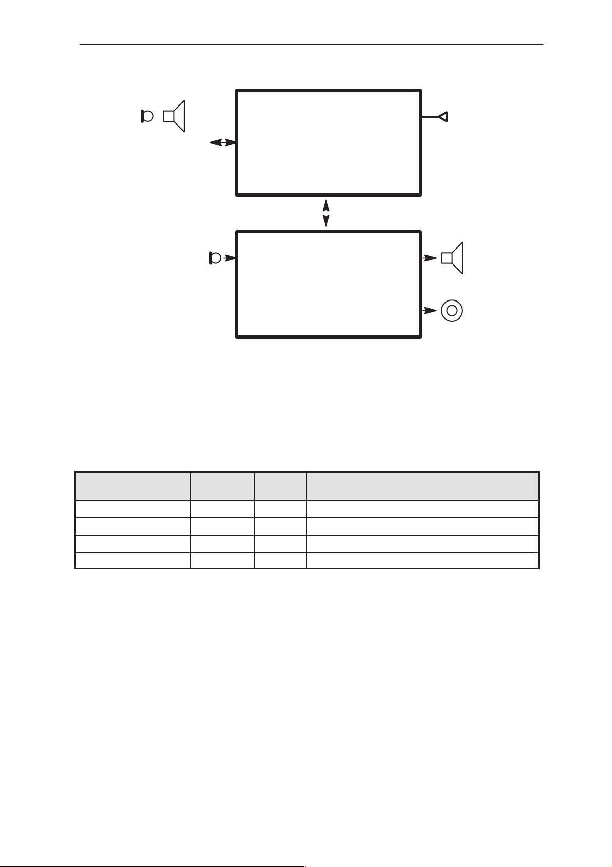
Module Description
The transceiver electronics consist of the Radio Module (RF + Baseband
blocks) and the UIF Module. The UIF Module is connected to the Radio
Module with a 30 pin connector. BaseBand blocks and RF blocks are
interconnected with PCB wiring. The Radio Module receives power from
the Battery via a 4 pin connector located at the bottom of the PCB. The
Transceiver is connected to accessories via a bottom system connector
with charging and accessory control.
General Information
The Radio Module provides the MCU and DSP environments, Logic
control IC (CDMA ASIC), memories, audio processing and RF control
hardware (CDRFI). On board power supply circuitry delivers operating
voltages for both BaseBand and UIF modules.
The UIF Module is a flex circuit with 4 blocks–– keyboard, display, buzzer,
and audio (earphone and microphone). The buzzer block contains a high
current amplifer circuit to drive the buzzer. LEDs are provided for
keyboard and LCD back lighting.
The RF block is designed for a hand portable phone, which operates in
CDMA PCS systems. The purpose of the RF module is to receive and
demodulate a radio frequency signal from the base station and to transmit
a modulated RF signal to the base station. The RF parts are designed for
power class II.
The system part provides MCU and DSP environments, memories, audio
processing, and RF control hardware. On board power supply circuitry
delivers operating voltage for both system and RF parts.
Issue 1 04/99
Page 2–3
Page 12
NHP–4
PAMS
General Information
HANDS FREE
BA TTER Y
CHARGER
M2BUS
DBUS
Technical Documentation
EXT ANTENNA
Baseband / RF MODULE
SPEAKERMICROPHONE
UIF MODULE
BUZZER
Figure 1. Module Layout
List of Modules
Table 1. Nokia1 NHP–4
Name of module Type code Material
code
Transceiver CDMA PCS1900 0501146
User interface DU8D 0200521
System/RF GR2 0200996
Mechanics MNHP4 0261xxx Variable dependant on cover colour as listed
0261387 Woodgrain Nokia
0261789 Red Nokia
0261799 Blue Nokia
0261915 Woodgrain Primeco
Notes
Page 2–4
Issue 1 04/99
Page 13
PAMS
NHP–4
Technical Documentation
General Information
Units and Accessories
Table 2. List of Battery Packs
Design Type Technology Type Code Material
Code
Nokia1, CDMA Slim, 600 mAh NiMH BBH –1S 0670027
Nokia1, CDMA Std, 1100 mAh NiCd BBH–2H 0670030
Nokia1, CDMA Ext, 1700 mAh NiMH BBH –1H 0670028
Nokia1, CDMA Vibrator, 600 mAh NiMH BBT–1XV 0670119
Table 3. List of Chargers
Name Type Code Material Code Notes
Fast Travel Charger ACH–4U 0675012 USA model
Cigarette Lighter Charger LCH–2 0675005 Universal
Desktop Charger CHH–2 0675022 Universal
HF Desktop Charger CHH–8 0675026 Universal
AC Adapter ACS–6U 0680018 USA model, needed for CHH–8
Table 4. List of Mobile Installation Accessories
Name Type Code Material Code Notes
Mobile Holder MBH–6 0620009
Mobile HF Charging Holder MCH–8 0620010
HF Junction Box HFJ–3 0694009
External HF Speaker HFS–6 0692005
HF Microphone HFM–4 0690002 Original
HF Microphone HFM–10 0690009 New , ”mouse” type
Power Cable PCH–4 0730009
External Audio Handset HSU–1 0640047
Compact HF PHF–1 0700017
Power Cable LCP–2 0680022
Mounting Plate MKE–1 0650007
Swivel Kit HHS–1 0650006 3 screws
Swivel Kit HHS–6 0650019 4 screws
Cable Holder CKH–1 0620016
Issue 1 04/99
Page 2–5
Page 14
NHP–4
PAMS
General Information
Table 5. List of Data Accessories
Name Type Material code Notes
PC–Link Adapter DAU–2 0750029
Data Cable DKH–1 9780084 CHH–8 → PC Link
Data Cable DKH–2 0730041 Adapter Cable
Data Cable DKH–5 0730038 HP–PC Link
Table 6. List of General Accessories
Name Type code Material code Notes
Carry Strap SWH–1 0720005
Belt Clip BCH–2 0720022
Headset HFS–11 0690010 Over the head headset
Headset HDC–2 0694017 Button headset
Technical Documentation
Basic Specifications
Table 7. Basic Specifications
Parameter Notes
Cellular system CDMA PCS
TX frequency band 1850.000 ... 1910 MHZ
RX frequency band 1930.000 ... 1990 MHZ
Duplex spacing 80 MHZ
Number of RF channels 1200
Channel spacing 50 kHz
Power Class II
Maximum output power +23 DBM 200 MW (CDMA)
Method of frequency synthesis 4 Synthesizerz and 1 multiplier
Frequency control VCTCXO
Receiver type 1 IF
Modulator type I/Q–baseband
Operational Voltage 5.3V...8.8 V
Page 2–6
Issue 1 04/99
Page 15

PAMS
NHP–4
Technical Documentation
Technical Specifications
Modes of Operation
NHP–4 operates in two modes:
1. In digital mode it operates on digital sync, paging pilot and traffic
channel.
2. Test mode (Local mode) used for troubleshooting and diagnostic
testing.
DC Characteristics
Table 8. Supply Voltages and Current Consumption
Line Symbol Minimum Typical /
Nominal
VBAT 5.3 6.0 8.8 V
Maxi-
mum
General Information
Unit / Notes
VCHAR 11.0 12.0 13.5 V / chargers
VCHAR 730 800 870 mA / chargers
CURRENT CONS. 250 365 900 mA / in digital talk mode
CURRENT CONS 8 12 16 mA / dig. idle (Slotted mode)
Slot cycle : 2.56s
AC Characteristics
Table 9. General RF Specifications
TX frequency band 1850.000 ... 1910 MHz
RX frequency band 1930.000 ... 1990 MHz
Duplex spacing 80 MHz
Number of RF channels 1200
Channel spacing 50 kHz
Spurious emissions In transit band at ant conn. < –61 dBm (1MHz resolution bandwidth)
Spurious emissions In receive band at ant conn. < –81 dBm (1 MHz resolution bandwidth)
Spurious emissions outside RX and TX band at
ant conn.
< –47 dBm (30 kHz resolution bandwidth)
Issue 1 04/99
Page 2–7
Page 16

NHP–4
PAMS
General Information
Technical Documentation
Digital Mode
Table 10. Transmitter Specifications for CDMA mode
Transmitter Type One IF at 208.1 MHz, Linear
TX Channel Filtering FIR in ASIC, 3dB BW from 1KHz to 615KHz
TX Spurious Filtering 4th order for D/A anti–aliasing, 2 ceramic RF filters and Du-
plex for receive band noise and spurious attenuation
TX Power Class II
TX Power Amplifier type HBT MMIC
Linear TX output power range –50dBm to 23dBm minimum in a 1.23MHz BW
Maximum TX power control Adaptive limiter so TX power is limited to 23 dBm
TX duty cycle 1/1, 1/2, 1/4, 1/8 variable rate with random slots. A slot is
1.25mS. Rate is controlled by voice activity
Adjacent channel power –42dBc in a 30KHz BW for offsets > 1.25 MHz from center F
Spurious emissions out off transmit
band
TX noise floor at minimum TX pow-er–54dBm/1.23MHz (TX gate on), –60dBm/1.23MHz (TX gate
TX noise floor at RX band with
Max. output power
TX power control method Output_power (dBm) = –73dBm – Receive_power (dBm) +
TX power initial accuracy +/–9dB within value as specified by TX control method
FCC rules
off)
–173dBm/Hz at RX input port
TX offset (dB). TX is slotted mode
TX offset control method From base station with one increments or decrement every
1.25mS (but only during active transmit slot)
TX offset control step size 1dB +/–0.5, and +/–20% over 10 steps in same direction
TX gain control range 85 dB IF + 15 dB RF
Modulator type I/Q modulator, OQPSK format
I/Q Modulator phase error +/–6 deg (+/– 4 deg for D/A and filter)
I/Q Modulator gain balance +/–0.65dB (+/–0.35dB for D/A and filter)
Table 11 Receiver RF specification, CDMA mode
Characteristics Symbol Min Typ Max Unit
RX frequency range 1930 1990 MHz
IF frequency 128.1 MHz
1st LO frequency 2059.35 2116.85 MHz
2nd LO frequency 128.1 MHz
Receiver IF bandwidth 1.2288 MHz
Input signal level –104 –25 dBm
Input dynamic range 79 dB
Noise figure NF 10 dB
Page 2–8
Issue 1 04/99
Page 17
PAMS
NHP–4
Technical Documentation
Table 11 Receiver RF specification, CDMA mode (continued)
Reference noise bandwidth
(total receiver)
Single tone desensitization,
1.25MHz
Intermodulation spurious response level, 1.25/2.05MHz
Passband amplitude response
1 KHz
615 KHz
1250 KHz
>1250 KHz
Mean Square Passband
phase response, 1–630 KHz
(with base station phase
equalizer)
–30
(Pin=–101)
–43
(Pin=–101)
–21
(Pin=–79)
–77
–75
General Information
UnitMaxTypMinSymbolCharacteristics
1.2288 MHz
dBm
dBm
–3
–4
0.03 rad^2
dB
dB
dB
dB
Receiver gain 12 91 dB
Receiver gain tolerance range.
Without gain setting or A/D
AGC range
includes RF gain step and cal
AGC accuracy (output level
variation for inputs –104 to
–25 dBm)
Baseband output level
(single–ended), RL>10KOhm
Baseband output level variation over RX input level of
–104 to –25 dBm
I/Q Amplitude imbalance –0.75 0.75 dB
I/Q Phase imbalance –7.5 +7.5 deg
Table 12 Reverse CDMA channel signals
103
(105
w/AtoD)
–.5 +.5 dB
–0.5 0.5 dB
110 dB
48 mVrms
8
(9
w/AtoD)
dB
Parameter Value / Notes
Bandwidth Occupied +/– 900 KHz –42 dBc In A Bandwidth Of 30
KHz
Spurious Emission in 1.23 MHz
–80 dBm
Band In Mobile Receive Band
Convolutionally Encoded, Block Interleaved, Modulated By 64–Ary
Orthogonal Modulation And Direct–Sequence Spread
Issue 1 04/99
Page 2–9
Page 18
NHP–4
PAMS
General Information
Technical Documentation
Mechanical Characteristics
Metric Units
Table 13. Mechanical Characteristics in Metric Units
Unit Dimensions
(mm)
(W x H x D)
Transceiver with standard
battery pack
Transceiver with standard
battery pack
Transceiver without battery
pack
Transceiver without battery
pack
Radio module 143x50x7 48 Common
UIF module 141x50x4 22
56x148x25 238 179 Nokia 1
56x148x25 241 179 US CDMA
56x148x25 134 137 Nokia 1
56x148x25 137 137 US CDMA
Weight
(g)
Volume
(cm3)
Notes
Mechanics 62 ...
67
Battery pack 600 mAh 56x101x8 104 42 NiMH, standard battery
Battery pack 1100 mAh 56x101x20 162 90 NiCd
Battery pack 1700 mAh 56x101x20 188 90 NiMH
depends on design version
English Units
Table 14. Mechanical Characteristics in English Units
Unit Dimensions
(in.) (W x H x
D)
Transceiver with standard
battery pack
Transceiver with standard
battery pack
Transceiver without battery
pack
Transceiver without battery
pack
Radio module 5.6x2.0x0.28
UIF module 5.6x2.0x0.16
Mechanics 2.19 ...
Battery pack 600 mAh 2.2x4.0x0.31
2.2x5.8x0.98
2.2x5.8x0.98 8.50 10.9 US CDMA
2.2x5.8x0.98
2.2x5.8x0.98 4.83 8.36 US CDMA
Weight
(oz.)
8.39
1.69
0.76
2.36
3.67
Volume
(in-
ches3)
10.9 Nokia 1
Nokia 1
8.36
Common
depends on design version
2.56
NiMH, standard battery
Notes
Page 2–10
Issue 1 04/99
Page 19
PAMS
NHP–4
Technical Documentation
Table 14. Mechanical Characteristics in English Units (continued)
Unit
Battery pack 1100 mAh 2.2x4.0x0.31
Battery pack 1700 mAh 2.2x4.0x0.31
Battery pack vibra NiMH
Dimensions
(in.) (W x H x
D)
Weight
(oz.)
5.71
6.63
(in-
ches3)
5.49
5.49
NiCd
NiMH
System Connector
Charging Connectors
Battery Connector
1
2
+
34
18
916
–
4
General Information
NotesVolume
123
System Connector
Figure 2. System Connectors
Table 15. List of Connectors
Connector Name Notes
Battery 4 connector pins
Charging Portable chargers: 3.8 mm DC plug and
contacts for Desk Stand
System/Data Centronix type, 16 pin, M2BUS, power
supply and audio signals.
ANTENNA
UIF 30 pin flex connector –
(not shown in picture)
Issue 1 04/99
Page 2–11
Page 20
NHP–4
S
19200 bits/s is in use in
S
/
System
CHAR
age (unloaded)
System
DSYN
PAMS
General Information
Pin /
Conn
1 /
System GND
2 /
System
3 /
System AGND
4 /
ystem
5 /
System M2BU
Line
Sym-
bol
XMIC
JCON
N
TDA
S
Minimum Typical /
3.0 V 3.15 V 3.30 V State ”1”
–.3 V 0.0 V 0.63 V State ”0”
0 V 0.0 V 0.7 V Input low
3.0V 4.9 V Input high
0 V 0.0 V 0.35V Output low
3.6V 4.65V 4.9 V Output high
Table 16. System Connector
Maximum Unit / Notes
Nominal
Digital ground
200
mV
rms
420
mV
rms
Analog ground
level
level
level
level
Technical Documentation
External audio input
from accessories or
handsfree microphone
DBUS data to the accessories
Serial bidirectional data
and control bus
Isink < 5 mA, baud rate
9600 bits/s. Baud rate
field test environment
6 /
ystem HOOK
7 /
System PHFS/
8 /
9 /
System
10 /
System XEAR/
RXD2
TXD2
+
GND Digital ground
HF–
PWR
–.3V 0.0 V 0.63V Hook on
2.5 V 3.15V 3.3 V Hook off
–.3V 0.0 V 0.63V Output low
level
2.5 V 3.15V 3.30V Output high
level
–.3V 0.0 V 0.63V Output low,
power off
2.5V 3.15V 3.30V Output high,
power on
–.3V 0.0 V 0.63V Output low
level
2.5V 3.15V 3.30V Output high
level
10.0V 12 V 13.5V
730 mA 800 mA 870 mA Vin < 11 V
130
mV
rms
410 mV-
rms
nom. DC–
level 2.0V
HOOK indication
Flash data
Hands–free device
power on/off
Flash data
Battery charging volt-
External output to accessories or handsfree
speaker and HF box
power turn on/off
11 /
Page 2–12
C
2.5V 3.15V 3.30V State ”1”
–.3V 0.0 V 0.63V State ”0”
DBUS sync
Issue 1 04/99
Page 21
PAMS
S
S
System
CHAR
age
transceiver
jack for LCH–2 or ACH–4
CHH–2
NHP–4
Technical Documentation
Table 16. System Connector (continued)
Pin /
Conn
12 /
ystem
13 /
System VAHS
14 /
System
15 /
ystem DCLK
16 /
Sym-
bol
RDA
VF 11.4 V 12.0V 12.6V Programming voltage for flash
+
MinimumLine
2.5V 3.15V 3.30V State ”1”
–.3V 0.0 V 0.63V State ”0”
2.5V 3.15V 3.30V Headset voltage
2.5V 3.15V 3.30V State ”1”
–.3V 0.0 V 0.63V State ”0”
10.0V 12 V 13.5V
730mA 800mA 870mA Vin < 11 V
General Information
Unit / NotesMaximumTypical /
Nominal
DBUS data from the
accessories
DBUS–clock
Battery charging volt-
Table 17. Battery Connector
Pin /
Conn
1 /
Battery
2 /
Battery
3 /
Battery
4 /
Battery
Pin /
Conn
1 / Char VCHAR
2 / Char GND
3 / Char VCHAR
4 / Char GND
Line
Symbol
VBAT 4.0 V 6.0 V 8.6 V Battery voltage for transceiver
BSI
BTEMP Battery temperature indicator, voltage at 25 oC
GND Power supply ground
Line
Symbol
Minimum
136 160 184 600 mAh
201 237 272 800 mAh
316
441 519 596 1700 mAh
Minimum
11.0 V 12.0 V 13.5 V
11.0 V 12.0 V 13.5 V
Typi-
cal /
Nom
372
Table 17. Battery Connector
Typi-
cal /
Nom
Maxi-
mum
427
Maxi-
mum
(NiMH)
(NiMH)
1200 mAh (Ni-
Cad)
(NiMH)
22 kohm pull–up resistor in transceiver
3.8 mm DC
No Load
Metal plates for charging in
Unit / Notes
Battery size indication.
Direct A/D result
100 k pull–up resistor in
Unit / Notes
IMPORTANT: These inputs are not to be used as power input pins.
Issue 1 04/99
Page 2–13
Page 22

NHP–4
PAMS
General Information
Technical Documentation
[This page intentionally left blank]
Page 2–14
Issue 1 04/99
Page 23

Programme’s After Market Services
NHP–4 Series Transceivers
Chapter 3
System Overview
Issue 1 04/99
Page 24

NHP–4
System Overview
Technical Documentation
CONTENTS
Acronyms 3–4. . . . . . . . . . . . . . . . . . . . . . . . . . . . . . . . . . . . . . . . . . . . . . . . . . . . . . .
Cellular History 3–5. . . . . . . . . . . . . . . . . . . . . . . . . . . . . . . . . . . . . . . . . . . . . . . . . .
Code Division Multiple Access (CDMA) 3–6. . . . . . . . . . . . . . . . . . . . . . . . . .
Quadrature Phase Shift Keying – QPSK 3–9. . . . . . . . . . . . . . . . . . . . . . .
The CDMA Signal 3–10. . . . . . . . . . . . . . . . . . . . . . . . . . . . . . . . . . . . . . . . . .
Processing Gain 3–11. . . . . . . . . . . . . . . . . . . . . . . . . . . . . . . . . . . . . . . . . . .
The CDMA Forward Link 3–12. . . . . . . . . . . . . . . . . . . . . . . . . . . . . . . . . . . .
V ocoder 3–13. . . . . . . . . . . . . . . . . . . . . . . . . . . . . . . . . . . . . . . . . . . . . . . . . . .
Convolutional Encoder 3–13. . . . . . . . . . . . . . . . . . . . . . . . . . . . . . . . . . . . . .
Interleaver 3–14. . . . . . . . . . . . . . . . . . . . . . . . . . . . . . . . . . . . . . . . . . . . . . . . .
PAMS
Page No
PN Code Generation 3–14. . . . . . . . . . . . . . . . . . . . . . . . . . . . . . . . . . . . . . .
Long Code Scrambling 3–16. . . . . . . . . . . . . . . . . . . . . . . . . . . . . . . . . . . . . .
Walsh Code User Channelization 3–16. . . . . . . . . . . . . . . . . . . . . . . . . . . . .
Walsh Codes 3–17. . . . . . . . . . . . . . . . . . . . . . . . . . . . . . . . . . . . . . . . . . . . . .
Orthogonal Functions 3–18. . . . . . . . . . . . . . . . . . . . . . . . . . . . . . . . . . . . . . .
Short Code Spreading 3–24. . . . . . . . . . . . . . . . . . . . . . . . . . . . . . . . . . . . . .
Forward Link Channel Format 3–24. . . . . . . . . . . . . . . . . . . . . . . . . . . . . . . .
CDMA Reverse Link 3–27. . . . . . . . . . . . . . . . . . . . . . . . . . . . . . . . . . . . . . . . . . .
Data Burst Randomizer 3–27. . . . . . . . . . . . . . . . . . . . . . . . . . . . . . . . . . . . .
Reverse Link Error Protection 3–28. . . . . . . . . . . . . . . . . . . . . . . . . . . . . . . .
64–ary Modulation 3–28. . . . . . . . . . . . . . . . . . . . . . . . . . . . . . . . . . . . . . . . . .
Reverse Channel Long Code Spreading 3–28. . . . . . . . . . . . . . . . . . . . . . .
Reverse Channel Short Code Spreading 3–28. . . . . . . . . . . . . . . . . . . . . .
Mobile Phone Operation 3–29. . . . . . . . . . . . . . . . . . . . . . . . . . . . . . . . . . . . . . .
Pilot Channel 3–29. . . . . . . . . . . . . . . . . . . . . . . . . . . . . . . . . . . . . . . . . . . . . .
Sync Channel 3–30. . . . . . . . . . . . . . . . . . . . . . . . . . . . . . . . . . . . . . . . . . . . . .
Paging Channel 3–30. . . . . . . . . . . . . . . . . . . . . . . . . . . . . . . . . . . . . . . . . . . .
Page 3–2
CDMA Call Initiation 3–31. . . . . . . . . . . . . . . . . . . . . . . . . . . . . . . . . . . . . . . .
Reverse Link Open Loop Power Control 3–31. . . . . . . . . . . . . . . . . . . . . . .
CDMA Call 3–32. . . . . . . . . . . . . . . . . . . . . . . . . . . . . . . . . . . . . . . . . . . . . . . .
Reverse Link Closed Loop Power Control 3–32. . . . . . . . . . . . . . . . . . . . .
CDMA Variable Rate Speech Coder 3–32. . . . . . . . . . . . . . . . . . . . . . . . . .
Mobile Power Bursting 3–32. . . . . . . . . . . . . . . . . . . . . . . . . . . . . . . . . . . . . .
The Rake Receiver 3–33. . . . . . . . . . . . . . . . . . . . . . . . . . . . . . . . . . . . . . . . .
CDMA Hand–offs 3–34. . . . . . . . . . . . . . . . . . . . . . . . . . . . . . . . . . . . . . . . . .
Issue 1 04/99
Page 25

PAMS
NHP–4
Technical Documentation
System Overview
List of Figures
Figure 1. TDMA & CDMA Freq and time domain 3–6. . . . . . . . . . . . . . . . . . . .
Figure 2. CDMA Capacity gains 3–7. . . . . . . . . . . . . . . . . . . . . . . . . . . . . . . . . . .
Figure 3. TDMA & CDMA Structure 3–8. . . . . . . . . . . . . . . . . . . . . . . . . . . . . . .
Figure 4. BPSK Modulator 3–9. . . . . . . . . . . . . . . . . . . . . . . . . . . . . . . . . . . . . . .
Figure 5. I/Q Modulator 3–10. . . . . . . . . . . . . . . . . . . . . . . . . . . . . . . . . . . . . . . . . .
Figure 6. CDMA Waveforms 3–10. . . . . . . . . . . . . . . . . . . . . . . . . . . . . . . . . . . . . .
Figure 7. CDMA Forward Link 3–12. . . . . . . . . . . . . . . . . . . . . . . . . . . . . . . . . . . .
Figure 8. Convolutional encoder 3–13. . . . . . . . . . . . . . . . . . . . . . . . . . . . . . . . . .
Figure 9. Interleaver 3–14. . . . . . . . . . . . . . . . . . . . . . . . . . . . . . . . . . . . . . . . . . . . .
Figure 10. PN Code generator 3–14. . . . . . . . . . . . . . . . . . . . . . . . . . . . . . . . . . . .
Figure 11. PN Code generator w/mask ckt. 3–15. . . . . . . . . . . . . . . . . . . . . . . . .
Page No
Figure 12. Mask offset example 3–16. . . . . . . . . . . . . . . . . . . . . . . . . . . . . . . . . .
Figure 13. CDMA Forward Link 3–16. . . . . . . . . . . . . . . . . . . . . . . . . . . . . . . . . .
Figure 14. Walsh code example 3–17. . . . . . . . . . . . . . . . . . . . . . . . . . . . . . . . . .
Figure 15. Orthogonal Functions. 3–18. . . . . . . . . . . . . . . . . . . . . . . . . . . . . . . . .
Figure 16. Walsh Encoding Example 3–19. . . . . . . . . . . . . . . . . . . . . . . . . . . . . .
Figure 17. Walsh Decoding Example 3–20. . . . . . . . . . . . . . . . . . . . . . . . . . . . . .
Figure 18. Definition of orthonogonality 3–21. . . . . . . . . . . . . . . . . . . . . . . . . . . .
Figure 19. Forward Link Channel Format 3–26. . . . . . . . . . . . . . . . . . . . . . . . . .
Figure 20. CDMA Reverse Link 3–27. . . . . . . . . . . . . . . . . . . . . . . . . . . . . . . . . . .
Figure 21. CDMA Pilot & Synch Channel Timing 3–29. . . . . . . . . . . . . . . . . . . .
Figure 22. Mobile Power Bursting 3–33. . . . . . . . . . . . . . . . . . . . . . . . . . . . . . . . .
Figure 23. CDMA Hand–off 3–34. . . . . . . . . . . . . . . . . . . . . . . . . . . . . . . . . . . . . .
Issue 1 04/99
Page 3–3
Page 26
NHP–4
Á
Á
Á
Á
Á
Á
Á
Á
Á
Á
Á
Á
Á
Á
Á
Á
System Overview
Acronyms
PAMS
Technical Documentation
AMPS
BS
ББББББББ
CDMA
CTIA
DAMPS
ББББББББ
DTMF
FDMA
GSM
ББББББББ
HLR
ISDN
MS
ББББББББ
MSC
MTSO
MTX
ББББББББ
NADC
Advanced Mobile Phone System
Base Station
БББББББББББББББББББББ
Code Division Multiple Access
Cellular Telecommunications Industry Association
Digital Advanced Mobile Phone System
БББББББББББББББББББББ
Dual Tone Multi Frequency
Frequency Division Multiple Access
Global System for Mobile communications
БББББББББББББББББББББ
Home Location Register
Integrated Services Digital Network
Mobile Station (Cellular phone)
БББББББББББББББББББББ
Mobile Switching Center (see MTX also)
Mobile Telephone Switching Office
Mobile Telephone Exchange (see MSC also)
БББББББББББББББББББББ
North American Digital Communications (IS–54 DAMPS)
PCH
PN Code
ББББББББ
PSTN
RF
SAT
ББББББББ
ST
TCH
TS
ББББББББ
VLR
VOCODER
VOCODER
Paging Channel
Pseudo random Noise Code
БББББББББББББББББББББ
Public Switched Telephone Network
Radio Frequency
Supervisory Audio Tone (5970, 6000 and 6030 Hz)
БББББББББББББББББББББ
Signaling Tone (10 kHz)
Traffic CHannel
Time Slot
БББББББББББББББББББББ
Visitor Location Register
VOice COder DEcodeR
VOice CODER
Page 3–4
Issue 1 04/99
Page 27

PAMS
NHP–4
Technical Documentation
System Overview
Cellular History
Mobile Radios have been in use for approximately 70 years and the cellular concept
was conceived in the 1940s. Public cellular mobile radio was not introduced in the
US until 1983.
In the beginning of the twentieth century, mobile radios were limited to shipboard
use due to the high power requirements and bulky tube radio technology.
Automotive systems in the 1920s operated on 6 volt batteries with a limited storage
capacity.
One of the first useful means of automotive mobile radio occurred in 1928 by the
Detroit police department. Transmission was broadcast from a central location and
could only be received by the mobile police radios.
Introduction of the first two way mobile application was delayed until 1933. This
simplex AM (Amplitude Modulation) push to talk system was introduced by the
police department in Bayonne, New Jersey. The first FM (Frequency Modulation)
mobile transmission (two frequency simplex) was used by the Connecticut State
Police at Hartford in 1940.
The first step towards mobile radio connection with the land line telephone network
was established in St. Louis in 1946. It was called an “urban” system and only
supported three channels.
In 1976, New York City had only 12 radio channels that supported 545 subscribers
with a waiting list of 3700.
In the 1970s, available cellular spectrum was constrained to frequencies above 800
MHz due to equipment design limitations and poor radio propagation characteristics
at frequencies above 1–GHz, this resulted in the allocation of the 825–890 MHz
region.
In 1974, 40 MHz of spectrum was allocated for cellular service and in 1986, an
additional 10 MHz of spectrum was added to facilitate expansion. The present
frequency assignments for the US Cellular system mobile phone is
824.040–848.970 MHz transmit and 869.040–893.970 MHz receive These bands
have been frequency divided (FDMA) into 30 kHz channels. This results in a
maximum capacity of 832 channels. These channels were then divided into two
groups with 416 channels assigned to each system.
Issue 1 04/99
Page 3–5
Page 28
NHP–4
System Overview
Code Division Multiple Access (CDMA)
PAMS
Technical Documentation
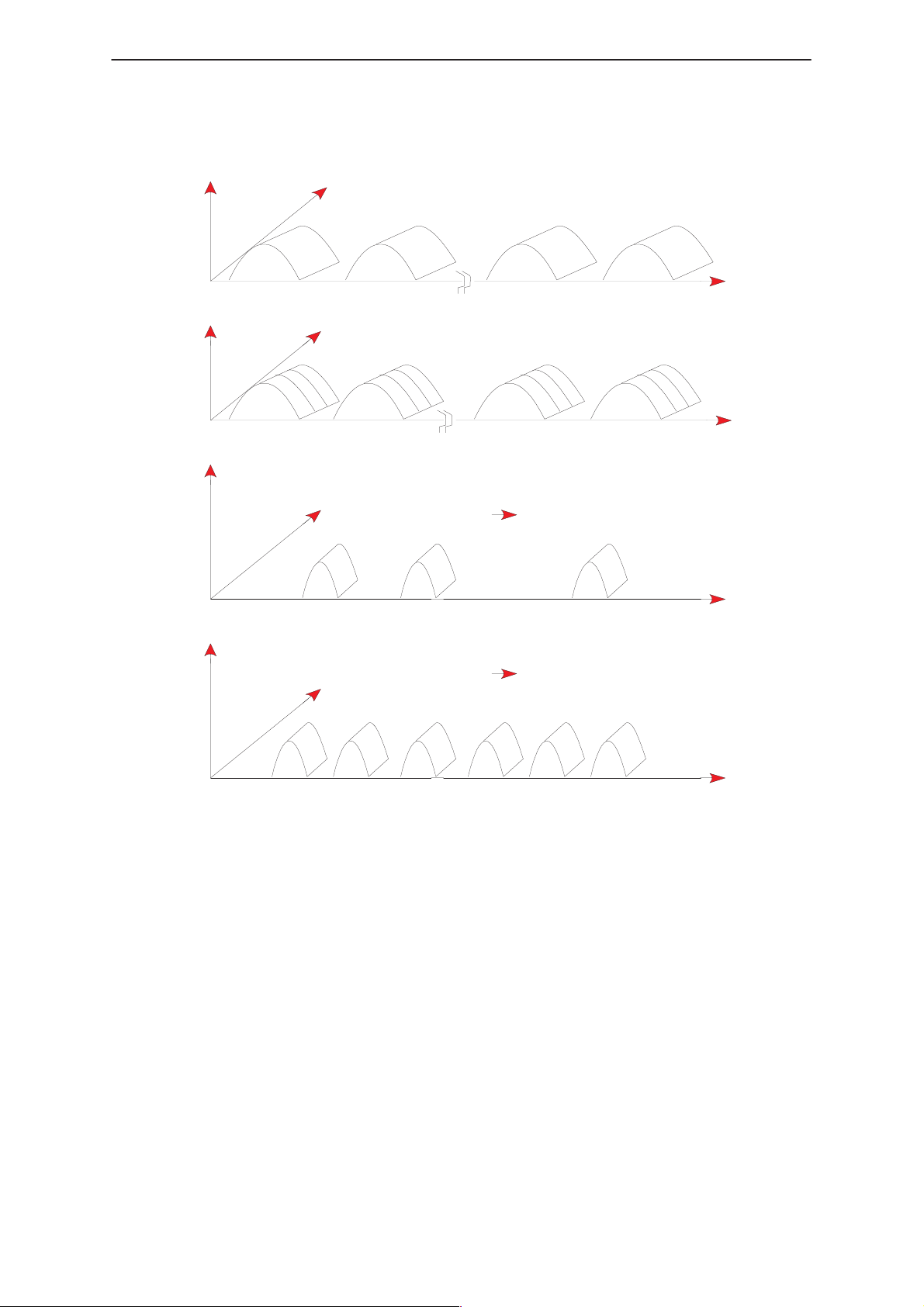
Amplitude
RX Ch1 RX Ch...n TX Ch 1 TX Ch...n
Amplitude Time
Amplitude
Time
Time
Channelization – FDMA
Channelization – TDMA
3
2
1
3
2
1
3
2
1
TX Ch...nTX Ch 1RX Ch...nRX Ch1
Channelization – CDMA
Forward Link B.S. M.S.
PN Offset 1 PN Offset 2 PN Offset 512
. . .
Frequency
3
2
1
Frequency
PN Sequence
(short code)
Channelization – CDMA
Amplitude
Time
CDMA01.DRW
Reverse LinkM.S. B.S.
Allows Channalization
and privacy
42
2
possible
PN Sequence
(long code)
Figure 1. TDMA & CDMA Freq and time domain
With FDMA Channelization (Analog AMPS), a channel is 30 kHz wide, this where all
the signal’s transmission power is concentrated. Different users are assigned
different frequency channels. FDMA is the acronym for Frequency Division Multiple
Access. Interference to and from adjacent channels is limited by the use of
bandpass filters that only pass signal’s within a specified narrow frequency band
while rejecting signals at other frequencies. The analog FM cellular system AMPS,
uses FDMA.
The US 800 MHz cellular system divides the allocated spectrum into 30 kHz
bandwidth channels. Narrowband FM modulation is used with AMPS, resulting in 1
call per 30 kHz of spectrum. Because of interference, the same frequency cannot
be used in every cell.
Page 3–6
Issue 1 04/99
Page 29

PAMS
NHP–4
Technical Documentation
System Overview
The frequency reuse factor is a number representing how often the same frequency
can be reused. To provide acceptable call quality, a Carrier–to–Interference ratio
(C/I) of at least 18 dB is needed. Practical results show that in most cases to
maintain a 18 dB (C/I) a frequency reuse factor of 7 is required. Please note that C/I
is carrier to interference, not signal to noise ratio The resulting capacity is one call
per 210 kHz of spectrum in each cell.
With TDMA, a channel consists of a time slot in a periodic train of time intervals
making up a frame. A given signal’s energy is confined to one of these time slots.
The IS–54B TDMA standard provides a basic modulation efficiency of three voice
calls per 30 kHz of bandwidth. The resulting capacity is one call per 70 kHz of
spectrum or three times that of the analog FM system.
With CDMA each signal consists of a different pseudo random binary sequence that
modulates the carrier, spreading the spectrum of the waveform. A large number of
CDMA signals share the same frequency spectrum. The signals are separated in
the receivers by using a correlator that accepts only signal energy from the selected
binary sequence and de–spreads its spectrum simultaneously. The other users’
signals, whose codes do not match, are not de–spread and as a result, contribute
only minimally to the noise and represent a self–interference generated by the
system. The forward link (B.S. to M.S.) “channels” are separated by offsets in the
short code PN sequence. Reverse link channels are separated by different long
code PN sequences. A detailed description of the forward and reverse links is
given later.
CDMA = 1.5 MHz 1 CDMA channel + 1.2288MHz
Capacity varies between 30 to 40 calls per CDMA
channel. Actual capacity depends Rho, processing
gain, error correction coding gain of M.S. vs signals
in cell and external cell signals.
AMPS = 1.5 MHz / 30kHz = 50 Channels
Capacity = 50 Channels / 7 (1 in 7 Frequency Reuse)
AMPS = 7 calls
DAMPS = 1.5 MHz / 30 kHz = 50 Channels
Capacity = 50 Channels / 7 x 3 Time Slots
DAMPS = 21 calls
GSM = 1.5 MHz / 200 kHz = 7 Channels
Capacity = 7 Channels / 7 x 8 Time Slots
GSM = 8 calls
Figure 2. CDMA Capacity gains
CDMA Capacity
Why should NOKIA go to so much trouble to develop CDMA? CAPACITY! To see
how CDMA increases capacity over present 800 MHz systems (AMPS and DAMPS)
lets look at a 1.5 MHz span of frequencies and compare. A CDMA frequency
channel is 1.2288 MHz wide however to provide guard bands in order to reduce
potential interference with adjacent analog channels a total of 1.5 MHz will be used.
Issue 1 04/99
Page 3–7
Page 30

NHP–4
System Overview
Technical Documentation
PAMS
The AMPS, DAMPS, and GSM capacity examples assume that only one channel
out of every seven can be used. In a crowded metropolitan area, cellular base
stations are arranged like the top part of Figure 3 Each base station is surrounded
by seven others so only one out every 7 channels can be used or adjacent channel
interference will occur. However, such is not the case for CDMA because all users
on a “CDMA Channel” operate on the same frequency. I’ve just used the word
“Channel” in a different way. Users in a given CDMA channel are separated by
different PN code sequences. According to information at the present time there
four designated CDMA frequency channels, so users on a given frequency channel
operate on the same frequency and are separated by different PN code sequences
which are also called “Channels”.
2
2
7
1
6
5
7
3
6
4
2
7
1
6
5
3
1
4
5
7
3
6
4
CDMA Cell Structure
Transmission range of
any given celll
1
1
ANALOG & TDMA Cell Structure
Transmission range of
any given cell
2
3
1
4
5
1
1
1
1
1
1
1
1
1
1
1
1
1
1
1
1
1
1
1
1
1
1
1
1
1
1
CDMA03.DRW
Page 3–8
Figure 3. TDMA & CDMA Structure
Issue 1 04/99
Page 31

PAMS
NHP–4
Technical Documentation
System Overview
Quadrature Phase Shift Keying – QPSK
Forward link transmissions from the Base Station (BS) to the Mobile Subscriber
(MS) use QPSK modulation. QPSK is the sum of Two Binary Shift Keyed (BPSK)
signals. Figure 4 shows how a BPSK signal is made up.
180
Time
0
TT
TT
Reference
carrier
input
Carrier
input
Carrier
input
DAMPS_4
A
T1 T2
B
++ ++
0 deg
–– ––
C
++
0 deg
––
Binary Phase Shift Keying
D1
D3
D4
D2
Binary input
D1 (on)
D3 and D4
(off)
D2 (on)
Binary 1
D1 (off)
D2 (off)
Binary 0
––
D3/D4
(on)
++
Modulator
output
Carrier
output
180 deg
Carrier
output
Binary
input
BPSK
output
Degrees
Radians
0 deg
10 1 10
0
TT
180
0
TT
TT
Binary input Output phase
Logic 0 180 deg
Logic 1 0 deg
Figure 4. BPSK Modulator
Before starting any explanation about phase modulation a convention needs to be
established that will carry on throughout this study guide. Digital signals are
generally generated by use of a modulator that generates a sine and a cosine
channel and scales each channel by a factor that ranges from –1 to +1. What
the last sentence means is that the values of Data Channels are –1 and +1, not
0 and 1. A logic one will be “plus one” and a logic zero will be “minus one”.
In drawing ”B” diodes D1 and D2 are forward biased into conduction with a logic
one. Transformer’s T1 and T2 are connected together in an in–phase condition. In
this case the output carrier’s signal would have the same phase as the input.
In drawing “C”diodes D3 and D4 are forwarded biased into conduction with a logic
zero. The output of T1 is cross connected to the input of T2 which will result in the
output being 180 degrees out of phase with the input signal.
Issue 1 04/99
Page 3–9
Page 32

NHP–4
System Overview
PAMS
Technical Documentation
I DATA
SIN
CARRIER
INPUT
Values of Data Channels
are –1 and 1, not 0 and 1
90
Hybrid
COS
o
Σ
For the reverse link
the Q data is delayed
CDMA04.DRW
Q DATA
by 1/2 clock chip. This
modulation is called
OQPSK (Offset Quadra
Phase Shift Keying)
Figure 5. I/Q Modulator
In Figure 5 the 90 phase shifter is used to generate the sine and cosine channel
reference frequency. The two signal paths are called the “In phase” and the
“Quadrature phase” paths, therefore the name, I/Q modulator.
The CDMA Signal
CDMA
Transmitter
CDMA
Receiver
1.25 MHz BW1.25 MHz BW
10 kHz BW10 kHz BW
Baseband
Data
9.6 kbps 19.2 kbps 1228.8 kbps
Background Noise
Encoding &
Interleaving
Walsh Code
Spreading
External Interference Other cell interference Other User Noise
Interference Sources
Walsh Code
Correlator
1228.8 kbps
Decode & De–
interleaving
19.2 kbps 9.6 kbps
Baseband
Data
CDMA05.DRW
Figure 6. CDMA Waveforms
To explain CDMA, some terms will have to be used that most persons are not
familiar with, but have patience they will be given a full explanation later in this Study
Guide. Forward link (BS to MS) CDMA starts with a narrowband signal that is
digitized speech. In this example the
full rate speech data rate
of 9600 bps is
shown.
Page 3–10
Issue 1 04/99
Page 33

PAMS
NHP–4
Technical Documentation
Speech data rates from the VOCODER can vary from 1200 BPS to 9600 BPS when
using “Rate Set One” and 14.4, 7.2, 3.6, and 1.8 kbps when using “Rate Set Two”.
A specialized digital code called a Walsh Code provides “user” channelization for the
forward link (B.S to M.S.) and is used to encode the reverse link (B.S. to M.S.) user
data. The short code PN sequence
reverse links. The short code also provides channelization for BASE STATIONS on
the forward link by using a masking circuit. Masking will be explained later.
Processing Gain
One of the unique aspects of IS–95 standard CDMA is 21 dB of processing gain.
Processing gain is computed by using the formula 10 log(spread data rate) divided
by (Symbol rate). [10 log (1,228,800 / 19.2kBPS) = 21 dB]. If you calculate the
processing gain using the numbers in the last sentence the answer is 18 dB. The
extra 3 dB is comes from the same data being transmitted by the Q channel. If rate
set 2 is used the processing gain is 19.31 dB. When “your” CDMA signal is
transmitted all other CDMA signals along with background noise and any spurious
signals are considered interference.
SPREADS
the baseband for both forward and
System Overview
When the wanted CDMA signal, “yours”, is received the correlation receiver
recovers “your” signal and rejects the rest. Looking at Figure 6, the upper right
most part of the drawing shows what happens to the unwanted signals. The
unwanted signals are not de–spread so that each interfering signal only contributes
a little to the noise floor while “your” wanted signal is de–spread and will have an
acceptable signal–to–noise ratio. This is where the processing gain comes into
play. The processing gain is 21 dB and it takes a signal–to–noise ratio of about 7
dB for acceptable voice quality. This leaves 14 dB of processing gain to extract
“your” signal from the noise.
Here are some of the differences between CDMA and analog FM (AMPS).
Multiple users are on one frequency at the same time. RF engineers have spent a
lot of time and effort trying to keep signals on one channel so that adjacent channel
signals would not cause interference. CDMA technology places a great many
conversations (signals) on the same frequency.
In CDMA a channel is defined by various digital codes in addition to having different
frequencies. Analog FM channels are defined by different frequencies only.
An analog FM (AMPS) cell site has a hard limit on the number of users it can
accommodate, only one call per frequency channel. CDMA has a soft capacity
limit. If cells surrounding a heavily loaded cell are lightly loaded then the heavily
loaded cell site can accommodate additional users. CDMA has a soft limit because
less “other cell” interference causes the total interference to be less. More calls can
also be accommodated at the expense of lower voice quality (S/N), this because
each additional user adds only a small amount of interference to the total.
Issue 1 04/99
Page 3–11
Page 34

NHP–4
System Overview
The CDMA Forward Link
PAMS
Technical Documentation
20 MSEC
BLOCKS
Vocoded
Speech
data
Convolutional
Encoder
9.6
kbps
1/2
Rate
Long Code
Generator
19.2
kbps
CDMA Forward Link
Interleaver
19.2
kbps
Long Code
Decimator
1.2288
Mbps
1 of 64 bits
XOR
Power
Control
Bit
1 in 24
Decimator
MUX
800 Hz
Walsh Cover
XOR
1.2288
Mbps
Walsh Code
Generator
1.2288
Mbps
1.2288
Mbps
I Short Code
I Channel
Lo Pass
Filter
To I/Q
Modulator
Lo Pass
Filter
Q Channel
Q Short Code
CDMA06,DRW
Figure 7. CDMA Forward Link
When discussing the CDMA Forward Link, voice data will be shown at 9600 BPS
(full rate). Keep in mind that the Vocoded Speech rate can be 9600, 4800, 2400 or
1200 BPS when using Rate Set One. The Vocoded Speech rate is developed after
the CODEC in both the Base Station and the Mobile Phone.
Speech data is passed through a Convolutional Encoder that doubles the data rate.
This data is then Interleaved. Interleaving does not change the data rate but will
introduce some data time delay. The Long Code Generator running at 1.2288
Mbps develops the 242 bits long PN (Pseudo–random noise) code. The long code
Decimator uses one out of every 64 bits of the PN long code and exclusive OR’s this
decimated bit stream with the output of the Interleaver. At this point the data stream
is still running at 19.2 kbps. The 64 bit Walsh Code Generator output running at
1.2288 Mbps is exclusive OR’ed with the pervious exclusive OR gate’s output. The
baseband is now running at a data rate of 1.2288 Mbps, 64 times 19.2 kbps. The
Walsh encoded data stream is then split into I and Q channels, and then each
channel is spread with a short code. Then finally, signals are sent through a low
pass filter to the I/Q modulators.
Page 3–12
Issue 1 04/99
Page 35

PAMS
NHP–4
Technical Documentation
System Overview
Vocoder
CDMA takes advantage of quiet times during speech to raise capacity. A variable
rate VOCODER is used; the vocoder’s output is at 9600 BPS when the user is
speaking. When the user pauses, or is listening, the data rate drops to 1200 BPS.
The data rates of 2400 and 4800 BPS are also used but not as often as the other
two. The data rate is based on speech activity and complexity. A decision is made
on the data rate every 20 msec. Normal speech has about a 40% activity factor. A
40% voice activity factor means that only 40% of transmission time is needed to
transmit the intelligible parts of speech.
Convolutional Encoder
Forward Error Protection
Data in
9600
pbs
D D D D
D D D D
Data Out
9600 bps
CDMA07.DRW
Data Out
9600 bps
Figure 8. Convolutional encoder
The forward CDMA link uses a half–rate convolutional encoder to provide error
correction capabilities. A half–rate encoder produces two output bits for every bit
input. This type of encoder accepts incoming serial data and outputs encoded data.
A convolutional encoder uses a shift register that contains a history of the bit
stream. It starts with all zeros and the data stream is shifted through. The two
9600 BPS output data streams are combined at a higher rate to provide a single
19,200 BPS data stream.
Issue 1 04/99
Page 3–13
Page 36

NHP–4
System Overview
Technical Documentation
PAMS
Interleaver
Data In Data Out
12
34
5 Interleaver
12345
Figure 9. Interleaver
CDMA08.DRW
Interleaving is the process of shuffling the data before transmission with a
corresponding un–shuffle on the receiving end. The purpose is to spread the bit
errors. Bit errors tend to come in bursts due to fading, rather than uniformly spread
in time. Interleaving provides a more uniform bit error distribution so that one burst
of errors will not wipe out a whole digital word but only individual bits that can be
corrected by the convolutional decoding.
PN Code Generation
Pseudorandom Noise (PN)Sequences
00 1
10 0 0
Pattern = 1001011
01 0 0
Figure 10. PN Code generator
1
CDMA09.DRW
The illustration above is a highly simplified version of a PN code generator. It will
be left to the reader to fill in the blank registers. This generator will start repeating
after 7 bits. A CDMA long code register is 42 bits long and the short code register
15 bits long.
Page 3–14
Issue 1 04/99
Page 37

PAMS
NHP–4
Technical Documentation
System Overview
The forward link Short Code is the same for all base stations. However a specific
mask is AND’ed with the output of the code generator to create a unique short code.
Even though the specific mask does not change the PN pattern the code is
considered unique relative to system time. This means that each specific mask will
shift the PN code to a unique delay with respect to system time and in this way the
shifted PN code is considered unique.
Here is another way of saying the same thing: PN codes used are required to have
low auto–correlation properties–––a time shifted version of itself correlated with itself
looks like random noise. Therefore a time shifted version is unique. Short Code
and Long Codes are handled the same: they use time shifted versions to be unique.
An example of a mask is shown in Figure 11. The three–bit shift register in
Figure 10 has a three–bit mask circuit connected to it in Figure 11.
11
0
11
1
0
11 1
11
11
0
0
0
0
00 1
11
00
1
0
0
0
0
10 0
11
00
1
0
11
0
0
1
1
1
0
0
0
1
11
11
Issue 1 04/99
1
0
0
1
1
0
0
0
11
1
1
0
CDMA10.DRW
0
0
1
Figure 11. PN Code generator w/mask ckt.
Page 3–15
Page 38

NHP–4
Á
Á
ÁÁ
ÁÁ
ÁÁ
Á
Á
Á
Á
Á
Á
Á
Á
Á
Á
Á
Á
Á
Á
ÁÁ
ÁÁ
Á
ÁÁ
ÁÁ
Á
Á
Á
Á
Á
Á
Á
ÁÁ
ÁÁ
Á
ÁÁ
ÁÁ
Á
Á
Á
Á
Á
Á
Á
ÁÁ
System Overview
PAMS
Technical Documentation
Offset
ÁÁ
ÁÁ
01
10
11
ÁÁ
100
101
110
ÁÁ
1111
T0
1
0
1
0
1
0
1
T1
ÁÁ
ÁÁ
0
0
0
ÁÁ
1
1
1
ÁÁ
1
T2
Á
Á
0
1
1
Á
0
0
1
Á
1
T3
Á
Á
1
0
1
Á
1
0
1
Á
0
T4
Á
Á
0
1
1
Á
1
1
0
Á
0
T5
ÁÁ
ÁÁ
1
1
0
ÁÁ
1
0
0
ÁÁ
1
T6
Á
Á
1
1
0
Á
0
1
1
Á
0
Base
БББББ
Stations
БББББ
1
2
БББББ
3
4
5
БББББ
6
7
Figure 12. Mask offset example
The above example shows how different offsets will create different codes. Note
that none of the codes has been altered. Each one just starts at a different time.
Remember the CDMA system uses the same 15 bit linear feedback shift register to
generate the PN short code for both forward and reverse links. If figure 28 were
expanded to a 15–bit shift register the time shifted short codes for the 512 base
station channels would be shown.
Long Code Scrambling
In the forward link the long code is used to scramble voice data and provide some
measure of security. However the complete long code is not used, refer to Figure
28. A Long Code Decimator allows only one in every 64 bits of the Long Code to
be exclusively OR’ed with the Encoded Voice Data. This scrambling does not
increase the data rate because two 19.2 kbps data streams are being exclusive
OR’ed with each other.
Walsh Code User Channelization
The CDMA forward link figure will be repeated here to show where we are in the
CDMA forward link (base station to mobile) generation.
20 MSEC
BLOCKS
1.2288
Mbps
1.2288
Mbps
I Short Code
Lo Pass
Filter
Lo Pass
Filter
Q Short Code
CDMA06,DRW
I Channel
To I/Q
Modulator
Q Channel
Vocoded
Speech
data
Convolutional
Encoder
1/2
Rate
9.6
kbps
19.2
kbps
Long Code
Generator
Interleaver
1.2288
Mbps
XOR
19.2
kbps
Long Code
Decimator
1 of 64 bits
Power
Control
Bit
1 in 24
Decimator
MUX
800 Hz
Figure 13. CDMA Forward Link
Walsh Cover
XOR
1.2288
Mbps
Walsh Code
Generator
The 20 msec VOCODED speech data blocks have had an error correction routine
added in the Convolutional Encoder that increased the data rate to 19.2 ksps (kilo
symbols per second).
Page 3–16
Issue 1 04/99
Page 39

PAMS
NHP–4
Technical Documentation
System Overview
The Interleaver changes the data order so only bits instead of whole words would be
lost because of data errors. The Long Code Generator generates a code that is
242 bits long. This code runs at 1.2288 Mbps and takes about 41.5 days before it
repeats. The PN (Pseudo–random) code is decimated by a factor of 64 that means
only one out of 64 bits is XOR’ed with the output of the Interleaver. The data rate at
this point is still 19.2 ksps because two 19.2 ksps data streams have been XOR’ed.
The 64 Walsh codes are used in the forward link as a means to uniquely identify
each user. The Walsh code generator runs at 1.2288 Mbps while the encoded
voice data runs at 19.2 kbps the ratio is 64 or 21 dB of processing gain. This
means that each data bit is XOR’ed with 64 Walsh code bits, one complete 64 bit
Walsh code. The voice data determines the polarity of the Walsh code. This
makes it easier for the CDMA mobile to find and decode its assigned Walsh code.
All base station’s use the same Walsh code 64 set. What gives each base station
its own unique identity will be explained in “Short Code Spreading”
The forward link is now running at its final rate of 1.2288 Mbps.
Walsh Codes
Walsh Codes in the CDMA forward link are used to “make” the CDMA forward
channels. Remember in analog phones a different frequency channel is used to
separate one cell phone user from another. TDMA cell phones use different time
slots to allow 3 phones to share one frequency channel. CDMA uses different
frequency channels like analog and TDMA cell phones. However, to separate
CDMA users on the same base station, different codes are used on the forward link
(Base Station to Mobile). IS–95 Standard CDMA uses Walsh code set 64. This
Walsh set has 64 unique codes each having 64 bits. Figure 14 shows how a Walsh
code set is built up.
W = 0
1
W =
2n
W W
W W
W =
W =
0 0
2
4
0 1
0 0 0 0
0 1 0 1
0 0 1 1
0 1 1 0
CDMA11.DRW
Figure 14. Walsh code example
Walsh code sets are generated by using the formula W2n = W W
W W .
In Walsh code set 2 it can be seen that the lower right digit is the logical not of the
other three digits. In Walsh code 4 the set 2 code is repeated three times with the
logical not being used in the lower right corner. The expansion number is always a
power of 2 and also notice that for each set the first code is always all zeros.
Issue 1 04/99
Page 3–17
Page 40

NHP–4
System Overview
Technical Documentation
PAMS
Walsh codes have the desirable characteristic of being “orthogonal” to each other.
What the heck does that mean(this is a rhetorical question)? ORTHOGONAL
Walsh Codes: when simultaneously transmitted they produce minimal interference
to other users. Look at the rows across in code set 4, any two rows have an equal
number of matches and mismatches. When correlation occurs between codes
(they match up) they will yield a cross correlation coefficient of 1. When the codes
do not match (correlate) the cross correlation coefficient is 0. Another way of
stating this is to say that when receiving the desired code a correlation receiver will
yield data and ignore all the unwanted codes.
Figure 15 should help sort out how Walsh orthogonal codes can keep different
CDMA users separated even though they are on the same frequency.
Orthogonal Functions
Two values are orthogonal if the result of exclusive–ORing them results in an equal
number of 1’s and 0’s.
Figure 15. uses the number 2 code, 0 1 0 1, in the Walsh code set 4 to
“Orthogonally Spread” some user input data. Each bit of user input data is
exclusive–OR’ed with the number 2 Walsh code that will result in TX Data shown in
Figure 15.
Orthogonal Functions:
Two values are orthogonal if the result of
exclusive–or–ing them results in an equal
number of 1’s and 0’s
Orthogonal Spreading:
Note; Each Orthogonal Sequence in the
forward link will have 64 bits rather than
the 4 bits in this example.
User Input 1 0 0 1 1
Orthogonal
Sequence
TX Data
Decoding using a Correct Orthogonal Function
RX Data 1 0 1 0 0 1 0 1 0 1 0 1 1 0 1 0 1 0 1 0
Correct
Function
0 1 0 1 0 1 0 1 0 1 0 1 0 1 0 1 0 1 0 1
1 0 1 0 0 1 0 1 0 1 0 1 1 0 1 0 1 0 1 0
+1
–1
0 1 0 1 0 1 0 1 0 1 0 1 0 1 0 1 0 1 0 1
1 1 1 1 0 0 0 0 0 0 0 0 1 1 1 1 1 1 1 1
10 011
+1
–1
EXAMPLE: 1 1 1 1
0 1 0 1
1 0 1 0
Page 3–18
Decoding with Incorrect Orthogonal Function
RX Data 0 1 0 1 0 1 0 1 0 1 0 1 0 1 0 1 0 1 0 1
Incorrect
Function
CDMA12.DRW
1 1 1 1 1 1 1 1 1 1 1 1 1 1 1 1 1 1 1 1
1 0 1 0 1 0 1 0 1 0 1 0 1 0 1 0 1 0 1 0
???? ?
+1
–1
Figure 15. Orthogonal Functions.
Issue 1 04/99
Page 41

PAMS
NHP–4
Technical Documentation
System Overview
When the number 2 Walsh code is exclusive OR’ed with what is now the “RX data”
each number 2 Walsh code yields the original user input data 4 times. The IS–95
CDMA standard uses a 64–bit Walsh code so the mobile cell phone has the
transmitted data repeated 64 times. When the data is repeated 64 times, your have
processing gain. Repeating the processing gain information: 10 log 64 equals 18
dB: another 3 dB is added because the data is modulated on two channels, I and Q
for a total of 21 dB. This is one of the reasons why IS–95 CDMA is so tolerant of
noise. That is to say a signal–to–noise ratio that would render an analog signal
useless works fine with CDMA.
BUT JUST HOW DOES AN ORTHOGONAL WALSH CODE SEPARATE
DIFFERENT USERS?
At first it would seem that broadcasting 25 to 30 code streams on one frequency
would create an “electronic tower of babel”. To explain how Walsh encoding works
a Walsh code set 2 that has 2 orthogonal Walsh codes will be used in Figure 16
User B
User B data 0110
1
0
For a 1 input
use code 01
For a 0 input
use code 10
For a 1 input,
use Code 00
For a 0 input,
use Code 11
+1
–1
+1
–1
User A data 1011
0
0
11
Walsh Encoding ExampleUser A
+1
0
W
2
0 1 – User B
0 0 – User A
=
–1
1
Channel A
Voice data
Channel A
Walsh Encoded
Voice Data
+1
111
0
0
Sum of A & B
Walsh Encoded
Data Streams
0
0
11
0000
+2
+1
–1
–2
Channel B
Voice Data
Channel B
Walsh encoded
Voice data
+1
0110
0
+1
1
00
–1
111
00
CDMA13.DRW
Figure 16. Walsh Encoding Example
This example uses Walsh Code set 2 that has two unique orthogonal codes, “00”
and “01”. Walsh code “00” will be assigned to User A and code “01” to User B.
Now in order for the Walsh code addition to work, bipolar values must be used, so
that a binary “0” has a value of “–1”. Also unless some higher math is utilized one
more convention must be used. If the voice data is a “0”, User A’s Walsh code is
“+1,+1”.
Issue 1 04/99
Page 3–19
Page 42

NHP–4
System Overview
Technical Documentation
PAMS
Here is how the “bipolar” addition works:
Voice data 1 0 1 1
bipolar Walsh code –1–1 +1+1 –1–1 –1–1
Walsh encoded data 0 0 1 1 0 0 0 0
The voice data is added to both bipolar Walsh code numbers. The example is for
User A.
If the two Walsh encoded voice data channels are added together the result is a
data stream that varies between +2 and –2. Walsh code decoding will show that
both user data streams are contained in this waveform and further more they do not
interfere with each other.
Original User A Voice Data
+1
+2
+1
–1
–2
Multiply summed data with desired Walsh
code then find the area under the
resultant curve.
+2
+1
111
0
0
+1
+2
+1
Original User B Voice Data
+1
+2
+1
–1
–2
Multiply summed data with desired Walsh
code then find the area under the
resultant curve.
+2
+1
0110
0
User A + B Walsh DataUser A + B Walsh Data
+1
+2
+1
X =
–1
–2
–1
00
–1
–2
=
1
CDMA14.DRW
X==
–1
–2
–1
–1
–2
–1
Figure 17. Walsh Decoding Example
To see how user data is recovered from the summed signal lets extract the first bit of
each users’ data. First remember that each user bit is XOR’ed with two Walsh code
bits in this example. Taking the first two summed data bits, multiply them with
desired Walsh code. For User A this results in a wave form that starts at zero for
the first bit period and goes to +2 in the second bit period, 0 X –1 = 0 and –2 X –1 =
+2. The next step requires a little calculus, very little to figure “the area under the
curve”. Since the waveform is a square wave its not to hard. Add the two resultant
bits and divide by the number of bit periods, (0 + 2) / 2 = 1. User A’s first data bit is
“1”.
Page 3–20
Issue 1 04/99
Page 43

PAMS
Á
Á
Á
Á
Á
Á
Á
Á
Á
Á
Á
Á
Á
Á
Á
Á
Á
Á
Á
Á
Á
Á
Á
Á
Á
Á
Á
Á
Á
Á
Á
Á
Á
Á
Á
Á
Á
Á
Á
Á
Á
Á
Á
Á
Á
Á
Á
Á
Á
Á
Á
Á
Á
Á
Á
Á
Á
Á
Á
Á
Á
Á
Á
Á
Á
Á
Á
Á
Á
Á
Á
Á
Á
Á
Á
Á
Á
Á
Á
Á
Á
Á
Á
Á
Á
Á
Á
Á
Á
Á
Á
Á
Á
Á
Á
Á
Á
Á
Á
Á
Á
Á
Á
Á
Á
Á
Á
Á
Á
Á
Á
Á
Á
Á
Á
Á
Á
Á
Á
Á
Á
Á
Á
Á
Á
Á
Á
Á
Á
Á
Á
Á
Á
Á
Á
Á
Á
Á
Á
Á
Á
Á
Á
Á
Á
Á
Á
Á
Á
Á
Á
Á
Á
Á
Á
Á
Á
Á
Á
Á
Á
Á
Á
Á
Á
Á
Á
Á
Á
Á
Á
Á
Á
Á
Á
Á
Á
Á
Á
Á
Á
Á
Á
Á
Á
Á
Á
Á
Á
Á
Á
Á
Á
Á
Á
Á
Á
Á
Á
Á
Á
Á
Á
Á
Á
Á
Á
Á
Á
Á
Á
Á
Á
Á
Á
Á
NHP–4
Technical Documentation
System Overview
To calculate User B’s first data bit multiply (0 X –1) and (–2 X 1) which equals zero,
minus two waveform. Find the area under the curve, (0 + (–2)) / 2 = –1, which is
User B’s first data bit.
It has been stated that Walsh codes are orthogonal and that this property results in
zero cross talk between Walsh code signals. Using bipolar numbers multiply Walsh
code “00” with Walsh code “01”. Add the resulting area and divide by the number of
bit periods and you will get zero. Figure 18 illustrates this.
+1
–1
Walsh code
0 0
00
+1
X=
0
–1
Figure 18. Definition of orthonogonality
Walsh code
0 1
+1
1
CDMA15.DRW
–1
Another and simpler way to state that Walsh codes are orthogonal is that since the
codes have an equal number of matches and mismatches, they are orthogonal.
The full 64–bit by 64 code Walsh code set 64 has been reproduced in the following
table.
Walsh Code Set W64
0
00
00
00
00
00
00
00
00
00
00
00
00
00
00
00
00
01
01
00
110
110
00
00
01
01
00
110
110
00
Á
00
Á
01
Á
01
Á
00
Á
110
Á
110
111
Á
110
Á
10
Á
110
Á
01
Á
00
Á
1
Á
1
00
Á
2
01
Á
3
01
Á
00
Á
110
Á
110
4
00
Á
5
00
Á
6
01
Á
7
01
Á
00
Á
110
Á
110
Á
00
Á
01
Á
01
Á
00
Á
110
Á
110
111
Á
110
Á
10
Á
110
Á
01
Á
00
Á
1
00
01
01
00
110
110
00
00
01
01
00
110
110
Á
00
Á
01
Á
01
Á
00
Á
110
Á
110
111
Á
110
Á
10
Á
110
Á
01
Á
00
Á
1
Á
00
Á
01
Á
01
Á
00
Á
110
Á
110
00
Á
00
Á
01
Á
01
Á
00
Á
110
Á
110
Á
00
Á
01
Á
01
Á
00
Á
110
Á
110
111
Á
110
Á
10
Á
110
Á
01
Á
00
Á
1
00
01
01
00
110
110
00
00
01
01
00
110
110
Á
00
Á
01
Á
01
Á
00
Á
110
Á
110
111
Á
110
Á
10
Á
110
Á
01
Á
00
Á
1
Á
00
Á
01
Á
01
Á
00
Á
110
Á
110
00
Á
00
Á
01
Á
01
Á
00
Á
110
Á
110
Á
00
Á
01
Á
01
Á
00
Á
110
Á
110
111
Á
110
Á
10
Á
110
Á
01
Á
00
Á
1
00
01
01
00
110
110
00
00
01
01
00
110
110
Á
00
Á
01
Á
01
Á
00
Á
110
Á
110
111
Á
110
Á
10
Á
110
Á
01
Á
00
Á
1
Á
00
Á
01
Á
01
Á
00
Á
110
Á
110
00
Á
00
Á
01
Á
01
Á
00
Á
110
Á
110
Á
00
Á
01
Á
01
Á
00
Á
110
Á
110
111
Á
110
Á
10
Á
110
Á
01
Á
00
Á
1
8
00
00
Á
9
00
Á
1
01
Á
0
01
Á
1
00
1
110
Á
110
Á
Á
00
Á
01
Á
01
Á
00
110
Á
110
Á
Issue 1 04/99
111
110
10
110
01
00
1
111
Á
110
Á
10
Á
110
Á
01
00
Á
1
Á
00
Á
00
Á
01
Á
01
Á
00
110
Á
110
Á
00
Á
00
Á
01
Á
01
Á
00
110
Á
110
Á
111
110
10
110
01
00
1
111
Á
110
Á
10
Á
110
Á
01
00
Á
1
Á
00
Á
00
Á
01
Á
01
Á
00
110
Á
110
Á
00
Á
00
Á
01
Á
01
Á
00
110
Á
110
Á
111
110
10
110
01
00
1
111
Á
110
Á
10
Á
110
Á
01
00
Á
1
Á
00
Á
00
Á
01
Á
01
Á
00
110
Á
110
Á
00
111
Á
00
110
Á
01
10
Á
01
110
Á
00
01
110
00
Á
110
1
Á
Page 3–21
111
Á
110
Á
10
Á
110
Á
01
00
Á
1
Á
Page 44

NHP–4
Á
Á
Á
Á
Á
Á
Á
Á
Á
Á
Á
Á
Á
Á
Á
Á
Á
Á
Á
Á
Á
Á
Á
Á
Á
Á
Á
Á
Á
Á
Á
Á
Á
Á
Á
Á
Á
Á
Á
Á
Á
Á
Á
Á
Á
Á
Á
Á
Á
Á
Á
Á
Á
Á
Á
Á
Á
Á
Á
Á
Á
Á
Á
Á
Á
Á
Á
Á
Á
Á
Á
Á
Á
Á
Á
Á
Á
Á
Á
Á
Á
Á
Á
Á
Á
Á
Á
Á
Á
Á
Á
Á
Á
Á
Á
Á
Á
Á
Á
Á
Á
Á
Á
Á
Á
Á
Á
Á
Á
Á
Á
Á
Á
Á
Á
Á
Á
Á
Á
Á
Á
Á
Á
Á
Á
Á
Á
Á
Á
Á
Á
Á
Á
Á
Á
Á
Á
Á
Á
Á
Á
Á
Á
Á
Á
Á
Á
Á
Á
Á
Á
Á
Á
Á
Á
Á
Á
Á
Á
Á
Á
Á
Á
Á
Á
Á
Á
Á
Á
Á
Á
Á
Á
Á
Á
Á
Á
Á
Á
Á
Á
Á
Á
Á
Á
Á
Á
Á
Á
Á
Á
Á
Á
Á
Á
Á
Á
Á
Á
Á
Á
Á
Á
Á
Á
Á
Á
Á
Á
Á
Á
Á
Á
Á
Á
Á
Á
Á
Á
Á
Á
Á
Á
Á
Á
Á
Á
Á
Á
Á
Á
Á
Á
Á
Á
Á
Á
Á
Á
Á
Á
Á
Á
Á
Á
Á
Á
Á
Á
Á
Á
Á
Á
Á
Á
Á
Á
Á
Á
Á
Á
Á
Á
Á
Á
Á
Á
Á
Á
Á
Á
Á
Á
Á
Á
Á
Á
Á
Á
Á
Á
Á
Á
Á
Á
Á
Á
Á
Á
Á
Á
Á
Á
Á
Á
Á
Á
Á
Á
Á
Á
Á
Á
Á
Á
Á
Á
Á
Á
Á
Á
Á
Á
Á
Á
Á
Á
Á
Á
Á
Á
Á
Á
Á
Á
Á
Á
Á
Á
Á
Á
Á
Á
Á
Á
Á
Á
Á
Á
Á
Á
Á
Á
Á
Á
Á
Á
Á
Á
Á
Á
Á
Á
Á
Á
Á
Á
Á
Á
Á
Á
Á
Á
Á
Á
Á
Á
Á
Á
Á
Á
Á
Á
Á
Á
Á
Á
Á
Á
Á
Á
Á
Á
Á
Á
Á
Á
Á
Á
Á
Á
Á
Á
Á
Á
Á
Á
Á
Á
Á
Á
Á
Á
Á
Á
Á
Á
Á
System Overview
1
00
111
Á
2
00
Á
1
01
Á
3
01
Á
1
00
Á
4
110
Á
1
110
5
Á
1
00
Á
6
00
Á
1
01
Á
7
01
1
00
Á
8
110
Á
1
110
Á
9
Á
2
00
0
00
Á
2
01
Á
1
01
Á
2
00
Á
2
110
Á
2
110
Á
3
Á
110
Á
10
Á
110
Á
01
Á
00
Á
1
Á
00
Á
00
Á
01
Á
01
00
Á
110
Á
110
Á
Á
111
110
Á
10
Á
110
Á
01
Á
00
Á
1
Á
111
110
10
110
01
00
1
00
00
01
01
00
110
110
00
00
01
01
00
110
110
00
Á
00
Á
01
Á
01
Á
00
Á
110
Á
110
Á
00
Á
00
Á
01
Á
01
00
Á
110
Á
110
Á
Á
111
110
Á
10
Á
110
Á
01
Á
00
Á
1
Á
00
Á
00
Á
01
Á
01
Á
00
Á
110
Á
110
Á
111
Á
110
Á
10
Á
110
01
Á
00
Á
1
Á
Á
111
110
Á
10
Á
110
Á
01
Á
00
Á
1
Á
111
Á
110
Á
10
Á
110
Á
01
Á
00
Á
1
Á
111
Á
110
Á
10
Á
110
01
Á
00
Á
1
Á
Á
00
00
Á
01
Á
01
Á
00
Á
110
Á
110
Á
111
110
10
110
01
00
1
111
110
10
110
01
00
1
111
110
10
110
01
00
1
00
Á
00
Á
01
Á
01
Á
00
Á
110
Á
110
Á
111
Á
110
Á
10
Á
110
01
Á
00
Á
1
Á
Á
00
00
Á
01
Á
01
Á
00
Á
110
Á
110
Á
00
Á
00
Á
01
Á
01
Á
00
Á
110
Á
110
Á
00
Á
00
Á
01
Á
01
00
Á
110
Á
110
Á
Á
00
00
Á
01
Á
01
Á
00
Á
110
Á
110
Á
111
Á
110
Á
10
Á
110
Á
01
Á
00
Á
1
Á
00
Á
00
Á
01
Á
01
00
Á
110
Á
110
Á
Á
111
110
Á
10
Á
110
Á
01
Á
00
Á
1
Á
Technical Documentation
111
00
00
110
10
110
01
00
1
00
00
01
01
00
110
110
00
00
01
01
00
110
110
Á
00
Á
01
Á
01
Á
00
Á
110
Á
110
Á
00
Á
00
Á
01
Á
01
00
Á
110
Á
110
Á
Á
111
110
Á
10
Á
110
Á
01
Á
00
Á
1
Á
Á
00
Á
01
Á
01
Á
00
Á
110
Á
110
Á
111
Á
110
Á
10
Á
110
01
Á
00
Á
1
Á
Á
111
110
Á
10
Á
110
Á
01
Á
00
Á
1
Á
111
Á
110
Á
10
Á
110
Á
01
Á
00
Á
1
Á
111
Á
110
Á
10
Á
110
01
Á
00
Á
1
Á
Á
00
00
Á
01
Á
01
Á
00
Á
110
Á
110
Á
111
110
10
110
01
00
1
111
110
10
110
01
00
1
111
110
10
110
01
00
1
PAMS
00
Á
00
Á
01
Á
01
Á
00
Á
110
Á
110
Á
111
Á
110
Á
10
Á
110
01
Á
00
Á
1
Á
Á
00
00
Á
01
Á
01
Á
00
Á
110
Á
110
Á
2
00
Á
4
00
Á
2
01
Á
5
01
Á
2
00
Á
6
110
Á
2
110
Á
7
2
00
Á
8
00
Á
2
01
Á
9
01
Á
3
00
Á
0
110
3
110
Á
1
Á
Page 3–22
00
Á
00
Á
01
Á
01
Á
00
Á
110
Á
110
Á
111
Á
110
Á
10
Á
110
Á
01
Á
00
1
Á
Á
111
110
10
110
01
00
1
111
110
10
110
01
00
1
111
Á
110
Á
10
Á
110
Á
01
Á
00
Á
1
Á
00
Á
00
Á
01
Á
01
Á
00
Á
110
110
Á
Á
111
Á
110
Á
10
Á
110
Á
01
Á
00
Á
1
Á
111
Á
110
Á
10
Á
110
Á
01
Á
00
1
Á
Á
111
Á
110
Á
10
Á
110
Á
01
Á
00
Á
1
Á
00
Á
00
Á
01
Á
01
Á
00
Á
110
110
Á
Á
00
00
01
01
00
110
110
00
00
01
01
00
110
110
00
Á
00
Á
01
Á
01
Á
00
Á
110
Á
110
Á
111
Á
110
Á
10
Á
110
Á
01
Á
00
1
Á
Á
00
Á
00
Á
01
Á
01
Á
00
Á
110
Á
110
Á
00
Á
00
Á
01
Á
01
Á
00
Á
110
110
Á
Á
00
Á
00
Á
01
Á
01
Á
00
Á
110
Á
110
Á
111
Á
110
Á
10
Á
110
Á
01
Á
00
1
Á
Á
111
110
10
110
01
00
1
111
110
10
110
01
00
1
111
Á
110
Á
10
Á
110
Á
01
Á
00
Á
1
Á
00
Á
00
Á
01
Á
01
Á
00
Á
110
110
Á
Á
111
Á
110
Á
10
Á
110
Á
01
Á
00
Á
1
Á
111
Á
110
Á
10
Á
110
Á
01
Á
00
1
Á
Á
111
00
00
01
01
00
110
110
00
00
01
01
00
110
110
00
Á
00
Á
01
Á
01
Á
00
Á
110
Á
110
Á
111
Á
110
Á
10
Á
110
Á
01
Á
00
1
Á
Á
Á
110
Á
10
Á
110
Á
01
Á
00
Á
1
Á
00
Á
00
Á
01
Á
01
Á
00
Á
110
110
Á
Á
Issue 1 04/99
Page 45

PAMS
Á
Á
Á
Á
Á
Á
Á
Á
Á
Á
Á
Á
Á
Á
Á
Á
Á
Á
Á
Á
Á
Á
Á
Á
Á
Á
Á
Á
Á
Á
Á
Á
Á
Á
Á
Á
Á
Á
Á
Á
Á
Á
Á
Á
Á
Á
Á
Á
Á
Á
Á
Á
Á
Á
Á
Á
Á
Á
Á
Á
Á
Á
Á
Á
Á
Á
Á
Á
Á
Á
Á
Á
Á
Á
Á
Á
Á
Á
Á
Á
Á
Á
Á
Á
Á
Á
Á
Á
Á
Á
Á
Á
Á
Á
Á
Á
Á
Á
Á
Á
Á
Á
Á
Á
Á
Á
Á
Á
Á
Á
Á
Á
Á
Á
Á
Á
Á
Á
Á
Á
Á
Á
Á
Á
Á
Á
Á
Á
Á
Á
Á
Á
Á
Á
Á
Á
Á
Á
Á
Á
Á
Á
Á
Á
Á
Á
Á
Á
Á
Á
Á
Á
Á
Á
Á
Á
Á
Á
Á
Á
Á
Á
Á
Á
Á
Á
Á
Á
Á
Á
Á
Á
Á
Á
Á
Á
Á
Á
Á
Á
Á
Á
Á
Á
Á
Á
Á
Á
Á
Á
Á
Á
Á
Á
Á
Á
Á
Á
Á
Á
Á
Á
Á
Á
Á
Á
Á
Á
Á
Á
Á
Á
Á
Á
Á
Á
Á
Á
Á
Á
Á
Á
Á
Á
Á
Á
Á
Á
Á
Á
Á
Á
Á
Á
Á
Á
Á
Á
Á
Á
Á
Á
Á
Á
Á
Á
Á
Á
Á
Á
Á
Á
Á
Á
Á
Á
Á
Á
Á
Á
Á
Á
Á
Á
Á
Á
Á
Á
Á
Á
Á
Á
Á
Á
Á
Á
Á
Á
Á
Á
Á
Á
Á
Á
Á
Á
Á
Á
Á
Á
Á
Á
Á
Á
Á
Á
Á
Á
Á
Á
Á
Á
Á
Á
Á
Á
Á
Á
Á
Á
Á
Á
Á
Á
Á
Á
Á
Á
Á
Á
Á
Á
Á
Á
Á
Á
Á
Á
Á
Á
Á
Á
Á
Á
Á
Á
Á
Á
Á
Á
Á
Á
Á
Á
Á
Á
Á
Á
Á
Á
Á
Á
Á
Á
Á
Á
Á
Á
Á
Á
Á
Á
Á
Á
Á
Á
Á
Á
Á
Á
Á
Á
Á
Á
Á
Á
Á
Á
Á
Á
Á
Á
Á
Á
Á
Á
Á
Á
Á
Á
Á
Á
Á
Á
Á
Á
Á
Á
Á
Á
Á
Á
Á
Á
Á
Á
Á
Á
NHP–4
Technical Documentation
3
00
00
00
Á
2
00
Á
3
01
Á
3
01
Á
3
00
Á
4
110
Á
3
110
5
Á
3
00
Á
6
00
Á
3
01
Á
7
01
3
00
Á
8
110
Á
3
110
Á
9
Á
4
00
0
00
Á
4
01
Á
1
01
Á
4
00
Á
2
110
Á
4
110
Á
3
Á
00
Á
01
Á
01
Á
00
Á
110
Á
110
Á
111
Á
110
Á
10
Á
110
01
Á
00
Á
1
Á
Á
00
00
Á
01
Á
01
Á
00
Á
110
Á
110
Á
00
01
01
00
110
110
00
00
01
01
00
110
110
111
110
10
110
01
00
1
00
Á
00
Á
01
Á
01
Á
00
Á
110
Á
110
Á
111
Á
110
Á
10
Á
110
01
Á
00
Á
1
Á
Á
111
110
Á
10
Á
110
Á
01
Á
00
Á
1
Á
00
Á
00
Á
01
Á
01
Á
00
Á
110
Á
110
Á
00
Á
00
Á
01
Á
01
00
Á
110
Á
110
Á
Á
00
00
Á
01
Á
01
Á
00
Á
110
Á
110
Á
00
Á
00
Á
01
Á
01
Á
00
Á
110
Á
110
Á
111
Á
110
Á
10
Á
110
01
Á
00
Á
1
Á
Á
00
00
Á
01
Á
01
Á
00
Á
110
Á
110
Á
00
00
01
01
00
110
110
00
00
01
01
00
110
110
111
110
10
110
01
00
1
00
Á
00
Á
01
Á
01
Á
00
Á
110
Á
110
Á
111
Á
110
Á
10
Á
110
01
Á
00
Á
1
Á
Á
111
110
Á
10
Á
110
Á
01
Á
00
Á
1
Á
111
Á
110
Á
10
Á
110
Á
01
Á
00
Á
1
Á
111
Á
110
Á
10
Á
110
01
Á
00
Á
1
Á
Á
111
110
Á
10
Á
110
Á
01
Á
00
Á
1
Á
111
Á
110
Á
10
Á
110
Á
01
Á
00
Á
1
Á
00
Á
00
Á
01
Á
01
00
Á
110
Á
110
Á
Á
111
110
Á
10
Á
110
Á
01
Á
00
Á
1
Á
111
110
10
110
01
00
1
111
110
10
110
01
00
1
00
00
01
01
00
110
110
111
Á
110
Á
10
Á
110
Á
01
Á
00
Á
1
Á
00
Á
00
Á
01
Á
01
00
Á
110
Á
110
Á
Á
00
00
Á
01
Á
01
Á
00
Á
110
Á
110
Á
System Overview
111
111
Á
110
Á
10
Á
110
Á
01
Á
00
Á
1
Á
111
Á
110
Á
10
Á
110
01
Á
00
Á
1
Á
Á
111
110
Á
10
Á
110
Á
01
Á
00
Á
1
Á
Á
110
Á
10
Á
110
Á
01
Á
00
Á
1
Á
00
Á
00
Á
01
Á
01
00
Á
110
Á
110
Á
Á
111
110
Á
10
Á
110
Á
01
Á
00
Á
1
Á
111
110
10
110
01
00
1
111
110
10
110
01
00
1
00
00
01
01
00
110
110
111
Á
110
Á
10
Á
110
Á
01
Á
00
Á
1
Á
00
Á
00
Á
01
Á
01
00
Á
110
Á
110
Á
Á
00
00
Á
01
Á
01
Á
00
Á
110
Á
110
Á
4
00
111
Á
4
00
Á
4
01
Á
5
01
Á
4
00
Á
6
110
Á
4
110
Á
7
4
00
Á
8
00
Á
4
01
Á
9
01
Á
5
00
Á
0
110
5
110
Á
1
Á
Á
110
Á
10
Á
110
Á
01
Á
00
Á
1
Á
00
Á
00
Á
01
Á
01
Á
00
Á
110
110
Á
Á
Issue 1 04/99
111
110
10
110
01
00
1
00
00
01
01
00
110
110
00
Á
00
Á
01
Á
01
Á
00
Á
110
Á
110
Á
00
Á
00
Á
01
Á
01
Á
00
Á
110
110
Á
Á
00
Á
00
Á
01
Á
01
Á
00
Á
110
Á
110
Á
111
Á
110
Á
10
Á
110
Á
01
Á
00
1
Á
Á
111
Á
110
Á
10
Á
110
Á
01
Á
00
Á
1
Á
111
Á
110
Á
10
Á
110
Á
01
Á
00
1
Á
Á
111
110
10
110
01
00
1
111
110
10
110
01
00
1
00
Á
00
Á
01
Á
01
Á
00
Á
110
Á
110
Á
111
Á
110
Á
10
Á
110
Á
01
Á
00
1
Á
Á
111
Á
110
Á
10
Á
110
Á
01
Á
00
Á
1
Á
111
Á
110
Á
10
Á
110
Á
01
Á
00
1
Á
Á
00
Á
00
Á
01
Á
01
Á
00
Á
110
Á
110
Á
111
Á
110
Á
10
Á
110
Á
01
Á
00
1
Á
Á
00
00
01
01
00
110
110
111
110
10
110
01
00
1
111
Á
110
Á
10
Á
110
Á
01
Á
00
Á
1
Á
111
Á
110
Á
10
Á
110
Á
01
Á
00
1
Á
Á
111
Á
110
Á
10
Á
110
Á
01
Á
00
Á
1
Á
00
Á
00
Á
01
Á
01
Á
00
Á
110
110
Á
Á
00
00
Á
00
00
Á
01
01
Á
01
01
Á
00
00
Á
110
110
Á
110
110
Á
00
00
Á
00
00
Á
01
01
Á
01
01
Á
00
00
Á
110
110
110
110
Á
Á
Page 3–23
111
Á
110
Á
10
Á
110
Á
01
Á
00
Á
1
Á
00
Á
00
Á
01
Á
01
Á
00
Á
110
110
Á
Á
Page 46

NHP–4
Á
Á
Á
Á
Á
Á
Á
Á
Á
Á
Á
Á
Á
Á
Á
Á
Á
Á
Á
Á
Á
Á
Á
Á
Á
Á
Á
Á
Á
Á
Á
Á
Á
Á
Á
Á
Á
Á
Á
Á
Á
Á
Á
Á
Á
Á
Á
Á
Á
Á
Á
Á
Á
Á
Á
Á
Á
Á
Á
Á
Á
Á
Á
Á
Á
Á
Á
Á
Á
Á
Á
Á
Á
Á
Á
Á
Á
Á
Á
Á
Á
Á
Á
Á
Á
Á
Á
Á
Á
Á
Á
Á
Á
Á
Á
Á
Á
Á
Á
Á
Á
Á
Á
Á
Á
Á
Á
Á
Á
Á
Á
Á
Á
Á
Á
Á
Á
Á
Á
Á
Á
Á
Á
Á
Á
Á
Á
Á
Á
Á
Á
Á
Á
Á
Á
Á
Á
Á
Á
Á
Á
Á
Á
Á
Á
Á
Á
Á
Á
Á
Á
Á
Á
Á
Á
Á
Á
Á
Á
Á
Á
Á
Á
Á
Á
Á
Á
Á
Á
Á
Á
Á
Á
Á
Á
Á
Á
Á
Á
Á
Á
Á
Á
Á
Á
Á
Á
Á
Á
Á
Á
Á
Á
Á
Á
Á
Á
Á
Á
Á
Á
Á
Á
Á
Á
Á
Á
Á
Á
Á
Á
Á
Á
Á
Á
Á
Á
Á
Á
Á
Á
Á
Á
Á
Á
Á
Á
Á
Á
Á
Á
Á
Á
Á
Á
Á
Á
Á
Á
Á
System Overview
5
00
111
Á
2
00
Á
5
01
Á
3
01
Á
5
00
Á
4
110
Á
5
110
5
Á
5
00
Á
6
00
Á
5
01
Á
7
01
5
00
Á
8
110
Á
5
110
Á
9
Á
6
00
0
00
Á
6
01
Á
1
01
Á
6
00
Á
2
110
Á
6
110
Á
3
Á
110
Á
10
Á
110
Á
01
Á
00
Á
1
Á
00
Á
00
Á
01
Á
01
00
Á
110
Á
110
Á
Á
111
110
Á
10
Á
110
Á
01
Á
00
Á
1
Á
00
00
01
01
00
110
110
111
110
10
110
01
00
1
111
110
10
110
01
00
1
111
Á
110
Á
10
Á
110
Á
01
Á
00
Á
1
Á
111
Á
110
Á
10
Á
110
01
Á
00
Á
1
Á
Á
00
00
Á
01
Á
01
Á
00
Á
110
Á
110
Á
111
Á
110
Á
10
Á
110
Á
01
Á
00
Á
1
Á
111
Á
110
Á
10
Á
110
01
Á
00
Á
1
Á
Á
111
110
Á
10
Á
110
Á
01
Á
00
Á
1
Á
00
Á
00
Á
01
Á
01
Á
00
Á
110
Á
110
Á
111
Á
110
Á
10
Á
110
01
Á
00
Á
1
Á
Á
00
00
Á
01
Á
01
Á
00
Á
110
Á
110
Á
111
110
10
110
01
00
1
00
00
01
01
00
110
110
00
00
01
01
00
110
110
00
Á
00
Á
01
Á
01
Á
00
Á
110
Á
110
Á
00
Á
00
Á
01
Á
01
00
Á
110
Á
110
Á
Á
111
110
Á
10
Á
110
Á
01
Á
00
Á
1
Á
111
Á
110
Á
10
Á
110
Á
01
Á
00
Á
1
Á
111
Á
110
Á
10
Á
110
01
Á
00
Á
1
Á
Á
111
110
Á
10
Á
110
Á
01
Á
00
Á
1
Á
00
Á
00
Á
01
Á
01
Á
00
Á
110
Á
110
Á
111
Á
110
Á
10
Á
110
01
Á
00
Á
1
Á
Á
00
00
Á
01
Á
01
Á
00
Á
110
Á
110
Á
Technical Documentation
111
00
00
110
10
110
01
00
1
00
00
01
01
00
110
110
00
00
01
01
00
110
110
Á
00
Á
01
Á
01
Á
00
Á
110
Á
110
Á
00
Á
00
Á
01
Á
01
00
Á
110
Á
110
Á
Á
111
110
Á
10
Á
110
Á
01
Á
00
Á
1
Á
Á
00
Á
01
Á
01
Á
00
Á
110
Á
110
Á
00
Á
00
Á
01
Á
01
00
Á
110
Á
110
Á
Á
00
00
Á
01
Á
01
Á
00
Á
110
Á
110
Á
111
Á
110
Á
10
Á
110
Á
01
Á
00
Á
1
Á
00
Á
00
Á
01
Á
01
00
Á
110
Á
110
Á
Á
111
110
Á
10
Á
110
Á
01
Á
00
Á
1
Á
00
00
01
01
00
110
110
111
110
10
110
01
00
1
111
110
10
110
01
00
1
PAMS
111
Á
110
Á
10
Á
110
Á
01
Á
00
Á
1
Á
111
Á
110
Á
10
Á
110
01
Á
00
Á
1
Á
Á
00
00
Á
01
Á
01
Á
00
Á
110
Á
110
Á
Short Code Spreading
The Forward Channel is spread one–more–time. The final spreading uses a Short
Code that is 215 (32,768) bits long, runs at 1.2288 Mbps and repeats every 26.667
msec. As previously stated all base stations use the same set of Walsh codes, a
short code combined with an “offset” mask allows each base station to have a
unique identification. These “PN Offsets” are separated by multiples of sixty–four
1.2288 Mbps clock chips which allows 512 unique time offsets for base station
identification (32768 bits / 64 bits = 512 offsets). By XOR’ing the Walsh encoded
channels with the offset short code, each base station can reuse all 64 Walsh codes
and be uniquely identified from other adjacent cells using the same CDMA
frequency channel.
Forward Link Channel Format
First of all remember the word “Channel” means a different “PN Code Sequence”
and not a different frequency for this part of the discussion.
A base station transmitter signal is a composite of at least 4 and as many as 42
different channels depending on interference and the Rho of the mobiles. Rho is a
figure of merit for specifying: percentage of transmitted power that correlates to the
ideal code.
Page 3–24
Issue 1 04/99
Page 47

PAMS
NHP–4
Technical Documentation
The “Pilot Channel” can be compared with the control channels used in analog.
The “Pilot Channel” is unmodulated Walsh code zero spread with Short Code that
has a unique mask applied in order for mobiles to identify cells from each other.
Pilot channel power is the strongest channel from the base station, with about 20%
of the total output power. The Pilot Channel provides the mobile with an easy to
demodulate strong signal that is used as a time reference.
The “Sync Channel” transmits timing information and always uses Walsh code 32
which is half zero’s and half one’s. The most important timing information contains
the state of the long code feedback shift registers 320 milli–seconds in the future.
The mobile can load this information into its long code generator, and start the
generator at the proper time. Long code state information is not all that is sent by
the sync channel but is one of the more important data.
The “Paging Channel” is the forward links digital control channel. Quite a lot of
information is sent to the mobile on this channel, a more complete discussion of all
four channels will be given in the section on how a CDMA mobile operates. The
first paging channel is always Walsh code one. If more paging channels are
needed Walsh codes 2 through 7 can be used.
System Overview
The “Traffic Channel” is the same thing as an analog voice channel. This is where
conversations take place. At least 55 Walsh codes are available for use as traffic
channels but the actual number that can be used is around 30 at present.
When all the various channels have been Walsh modulated they are split into I and
Q channels which are re–spread with the short code to provide base station identity,
filtered to reduce bandwidth and converted to analog signals. The analog I and Q
signals from all the channels are summed together and sent to the I/Q modulator for
modulation onto an RF carrier.
Issue 1 04/99
Page 3–25
Page 48

NHP–4
System Overview
Technical Documentation
PAMS
Figure 19, “Forward Link Channel Format “shows how the various channels are
made up.
W0
1.2288
Pilot Channel: All 0’s
MHz
+
Sync Channel
Data
1200 bps
Paging Channel
Data
9.6 kbps
4.8 kbps
2.4 kbps
Forward Traffic
Channel Data
9.6 kbps
4.8 kbps
2.4 kbps
1.2 kbps
User Long
Code mask
Convolutional
Encoder
Convolutional
Encoder
Paging Channel
Long Code Mask
Convolutional
Encoder
Long Code
Generator
Interleaver
Interleaver
Long Code
Generator
Interleaver
Long Code
Decimator
1 in 64 bits
19.2
kbps
19.2
kbps
+
+
4800
bps
Power
Control
Bit
MUX
W32
+
W 1 – 7
+
1.2288
MHz
1.2288
MHz
W 8–31 &
W 33–63
+
Summer
CDMA16.DRW
I Channel Short Code
Pilot PN Sequence
+
+
Q Channel Short Code
Pilot PN Sequence
Page 3–26
Figure 19. Forward Link Channel Format
Issue 1 04/99
Page 49

PAMS
NHP–4
Technical Documentation
System Overview
CDMA Reverse Link
20 msec
blocks
Vocoded
Speech
Data
Convolutional
Encoder
9.6
kbps
1/3
rate
Interleaver
28.8
kbps
6–bit
words
@ 4.8 k/s
28.8
kbps
Walsh
Code 63
Walsh
Code 62
Walsh
Code 61
Walsh
Code 2
Walsh
Code 1
Walsh
Code 0
1.2288 Mbps
Long Code
307.2
kbps
1.2288 Mbps
Data Burst
Randomizer
Figure 20. CDMA Reverse Link
The CDMA reverse link (Mobile to Base Station) is quite a bit different from the
forward link. The mobile does not have a pilot channel. This is because each
phone would have to have its own unique pilot channel and there are only 64 Walsh
codes, also the pilot channel power requirements would be severe for the mobile.
Because of the lack of a pilot channel and OQPSK (Offset Quadraphase Shift
Keyed) modulation the base station will have a tougher time demodulating the
mobiles signal. To give the reverse link better performance, a one–third rate
Convolutional Encoder is used and six data bits at a time is used to point at one of
the 64 Walsh codes. The last sentence will be explained shortly. The 307.2 kbps
data is XOR’ed with a long code that is unique for each CDMA cellular phone
creating a 1.2288 Mbps data stream. Finally, just like a base station the 1.2288
Mbps data stream is split and XOR’ed with an I & Q short code. The mobile cell
phone has one more process, the Q Channel is delayed by one–half clock period.
I Short Code
x
xx
Q Short Code
1/2 Chip
Delay
1/2
I
Q
Data Burst Randomizer
When the vocoder lowers its data rate, the mobile starts turning off its transmitter.
At the lowest data rate the mobile transmitter is only on one–eighth of the time. The
average output power will drop 3 dB each time the data rate is cut in half. Average
output power drops because the mobile’s transmit time is cut in half, the peak output
power does not change. Now if all the mobiles transmitted at the same time there
would not be any reduction of interference. The Data Burst Randomizer
randomizes the mobiles transmit time to keep them from transmitting at the same
time. Randomizing instructions come from the Frame Rate determination algorithm
and the Long Code state in the previous frame.
Issue 1 04/99
Page 3–27
Page 50

NHP–4
System Overview
Reverse Link Error Protection
To improve the reverse link performance a one–third rate convolutional encoder is
used. This encoder has one 9600 bps input and three 9600 bps outputs which
when combined result in a 28.8 kbps data stream. Each data bit is encoded with 3
error correction bits to improve the error correction rate. The forward link uses
one–half rate encoding.
64–ary Modulation
Remember that Walsh codes are orthogonal with each other, which means that
several can be broadcast on one frequency without interfering with each other. The
mobile does not XOR voice data with a Walsh code. Every six–bits of voice data is
used to select one of the 64 Walsh codes. 26 = 64, when six bits of voice data “1 0
1 1 0 1” for example, are converted to a base 10 number it equals 45. So instead of
XOR’ing “1 0 1 1 0 1” with one Walsh code, Walsh code 45 represents the six data
bits. Again the reason for using Walsh codes is because they are orthogonal with
each other, they do not interfere with each other. The six–bit words have a rate of
4800 words per second that means that 4800 64–bit Walsh codes are selected each
second. This works out to a data rate of 307.2 kbps.
Technical Documentation
PAMS
Reverse Channel Long Code Spreading
The long code shift register is 42 bits long, runs at a rate of 1.2288 Mbps, and
repeats it’s self approximately once every 41.5 days. Mobile cellular phones use
one of the 4.3 billion long codes for their reverse link channel, each mobile has its
own long code. The long codes are uncorrelated, which means they are all
different, but they are not orthogonal with each other. Not being orthogonal is a
draw–back but the base station knows when the mobiles long code started plus or
minus doppler and range uncertainty and this helps with correlation. High speed
searcher circuits in the base station allow a quick search over a wide range to lock
on a particular user’s signal. The long code at 1.2288 Mbps is XOR’ed with the
307.2 kbps data stream to create a 1.2288 Mbps data rate.
Reverse Channel Short Code Spreading
CDMA mobile phones use the same PN short code sequence as the base station’s
use, however the PN code’s purpose is different. The mobile’s use OQPSK (Offset
Quadraphase Shift Keyed). OQPSK is accomplished by adding a half period clock
delay to the mobile’s Q channel. OQPSK prevents the signal from going to zero
magnitude and greatly reduces the dynamic range of the modulated signal. Less
costly amplifiers can be used on CDMA mobiles because of the reduced linear
dynamic range obtained with OQPSK modulation. The mobile’s short code is not
delayed with a mask like the base stations short code is.
Page 3–28
Issue 1 04/99
Page 51

PAMS
NHP–4
Technical Documentation
System Overview
Mobile Phone Operation
When a CDMA mobile scans for the strongest Pilot Channel signal, the scanning is
done in time rather than frequency scanning like an analog phone does. Once the
strongest Pilot channel has been located, Sync Channel information is demodulated.
The sync channel contains information the mobile needs in order to decode the
Paging Channel. The Paging channel’s use can be compared to a digital control
channel for DAMPS phones When the mobile goes into a call a Traffic Channel is
used.
Pilot Channel
The Pilot Channel is transmitted continuously by the base station to provide mobiles
with pilot and sync channel timing. The only modulation on the Pilot Channel is
Walsh code zero XOR’ed with the Short Code The Short Code is 215, (32768) bits
long and at 1.2288 Mbps takes 26.67 msec before repeating its self. The start time
of any base station pilot channel is always an exact multiple of 64 system clock
cycles (called chips) offset in time from any other base station. The mobile checks
all 215 short code offsets to find the strongest pilot signal using the “searcher”
special hardware dedicated to doing pilot correlations. After checking all chip
offsets the mobile stores signal strengths of any Pilot Channel it hears. When the
strongest pilot signal is found the Rake demodulator aligns its self to the short code
offset, then applies Walsh code 32 in order to demodulate the Synch Channel. The
mobile knows when this Pilot channel and Synch Channel starts but it does not
know if it is time slot 1, 45, 248 or what. Figure 36 “CDMA Pilot & Synch Channel
Timing” will help you understand how the mobile gets timing and other information
from these two channels.
Master
Start
Time
PILOT CHANNEL
Received base
station pilot
channels
Time
Master
Start
Time
SYNC CHANNEL
Time
Figure 21. CDMA Pilot & Synch Channel Timing
The Pilot channel circle has small tick marks sticking outside the circle. These tick
marks represent signal strengths of the received Pilot channels from surrounding
base stations. Each base station’s pilot channel is separated from the next by 64
clock chips for a total of 512 different pilot channels. The longest tick on the right
side represents the strongest Pilot channel.
Issue 1 04/99
Page 3–29
Page 52

NHP–4
System Overview
Master (System) start time is shown on both circles but the mobile does not know
System start time until it decodes the Sync channel. Remember that both the Pilot
and Sync channels do not contain a Long Code so they both repeat at the same rate
of 26.67 msec. The mobile starts decoding the Synch channel information of the
strongest cell site when it acquires that cell’s Pilot channel. The mobile does not
decode Sync channels of the weaker cell sites received during the search.
Sync Channel
The Sync Channel has a lot of important information, some of which is listed below..
Pilot PN offset of base station: The Pilot PN offset is the base station’s time slot
number.
:
System Time
Local Time Offset from System Time:
Long Code State: This is very important! The state of the “Long Code” 320
milliseconds in the future is sent. The CDMA Long Code was started in Jan 1, 1980
and has been running ever since. Remember this code only repeats its self once
every 41 days, so it would take too long to search through the entire code. Not only
does the CDMA cellular phone need to know when the present long code sequence
started, it also needs to know where the code is “right now”. That’s what is meant
by “Code State”.
SID, NID of Cellular System: System Identification, Network Identification
Paging Channel Data Rate: 0, 9600: 1, 4800
Base Station Protocol Revision: 1 – IS95; 2 – IS95A; 3 – TSB74
Leap Seconds From Start of System Time: This is the delay from system time for
the clock based on the “slot cycle index”.
Daylight Savings Time Flag: Self explanatory.
Is the MASTER start time.
Technical Documentation
PAMS
Paging Channel
Once the mobile has system time and long code state, the Paging channel
information can be read. If required the mobile will register with the base station at
this time. The phone must register if it is in a slotted mode. When a phone is in a
slotted mode it goes to sleep for a few seconds periodically and then wakes up to
check for a page. The sleep period based on the “slot cycle Index” must be known
to the base station or the phone could be paged while asleep and miss the page.
The following is a partial list of Paging channel information:
System Parameters Message: This message provides the mobile with
information, such as network, system and base station identification numbers, the
number of paging channels supported, registration information, and the soft
hand–off thresholds.
Access Parameters Message: When a mobile calls the base station it uses a
channel called the “Access Channel”. This message gives the mobile information
that dictates the behavior of access probes when a CDMA mobile initiates a call.
Neighbor List Message: The neighbor list gives the mobile the PN Offsets of
surrounding cell sites that may become likely candidates for soft hand–offs.
Page 3–30
Issue 1 04/99
Page 53

PAMS
NHP–4
Technical Documentation
CDMA Channel List Message: The CDMA channel list reports the number of
CDMA frequencies supported by the cell station in use as well as surrounding cell
site frequencies and configurations.
Slotted Page Message: The Slotted and Non–slotted page messages allow the
cell site to page CDMA phones for incoming calls. CDMA mobiles operating in the
slotted mode must first register with the cell site before they can be paged. This
registration is required to establish which slot will be used by the cell site to transmit
the page to the mobile.
Channel Assignment Message: The channel assignment message is used to
communicate the information needed to get the mobile onto a traffic channel.
CDMA Call Initiation
When a user keys in a phone number and hits the send key the mobile sends out an
“Access Probe”. The “Access Channel” is one of the two channels used by a
mobile, it is used by the mobile to initiate calls, the other channel is the Traffic
channel. The difference between the two channels is in the coding. The Access
Channel applies a mask to the Long Code that is derived from information received
from the Sync and Paging channels: the information is; paging channel number,
access channel number, base station ID, and the Pilot PN offset used by the base
station. A new sub–subject comes up at this point, Power Control, which will be
discussed in the next sub–topics. Since a two–way link has not been established
yet, open loop power control will be used by the mobile to set its transmitter output
power. Multiple tries are allowed with random times between tries to prevent two
mobiles from consistently transmitting access probes at the same time.
System Overview
Reverse Link Open Loop Power Control
The key to maximizing CDMA capacity is power control. The limiting factor for
CDMA system capacity is total interference. Total interference can best be
described as all of the unwanted signals a base station receives. These signals
include other CDMA signals, natural back ground noise, and man made interference
such as noisy power lines. Ideally a base station would receive all the mobiles
signals at the same level. If the mobiles transmit a stronger signal than necessary
then more interference would be created and capacity would drop. When a CDMA
mobile first tries to contact a base station, open loop power control is used. Open
loop power control sets the sum of transmit and receive power to a constant, –73
dBm. The formula is; Transmit Power = (–73) – (Receive Power): all units are in
dBm. If a mobile received a base stations signal at –85 dBm the mobiles transmit
power would be (–73 dBm) – (–85 dBm) = +12 dBm transmit power.
The mobile’s Open Loop power control slew rate is limited to match the slew rate of
closed loop power control. If not limited the mobiles power output could swing
wildly during sudden reverse link signal strength changes.
A third point must be made before leaving Reverse Link Open Loop Power Control.
Suppose the CDMA mobile is traveling between two base stations, one has a large
area to cover and transmits signals at high output power.
Issue 1 04/99
Page 3–31
Page 54

NHP–4
System Overview
The second base station is a mini–cell and therefore transmits at a lower power.
The mobile would transmit a higher power than necessary to the mini–cell because
the weaker signal would be interrupted as a distant station. This problem is taken
care of after the mobile has located the strongest base station. Information
contained in the Sync Channel of each cell site transmits its characteristics for
power control.
CDMA Call
After each access attempt, the mobile listens to the Paging Channel for a response
from the base station. When the base station detects the mobiles access probe, it
responds with a channel assignment message. This message contains all of the
information required to get the mobile onto a traffic channel. Information required
for the mobile to start using a traffic channel includes, Walsh code channel to be
used for the forward traffic channel, the frequency being used, and the frame offset
to indicate the delay between the forward and reverse links. Once this information
has been acknowledged by the mobile a move to the designated traffic channel is
accomplished. At this point conversations can began. To accommodate traffic
other than voice data, two methods of temporarily seizing the traffic channel are
used: blank and burst signaling and dim and burst signaling. Blank and burst
signaling seizes several blocks of data frames, removes the voice data and replaces
it with house keeping data. Dim and burst reduces the VOCODER rate and then
uses the remaining traffic channel time to more slowly send house keeping
messages.
Technical Documentation
PAMS
Reverse Link Closed Loop Power Control
Because of multipath, atmospheric conditions, and the number of CDMA users
among other reasons the Open Loop Power Control method is not precise enough.
Remember to optimize capacity all CDMA mobile signals should arrive at the base
station at the same strength. The base station monitors each mobile’s receive
signal strength and directs the mobile to raise or lower it’s power in 1 dB steps until
the signal level is just adequate. One side benefit from lower power output is longer
battery life for the mobile.
CDMA Variable Rate Speech Coder
The VOCODER takes advantage of quiet times and less complex parts of speech to
raise capacity. An ”oooooo” vowel sound is less complex than a word like ”fat” or
”cat” with consonants in it. It takes more coded samples to reproduce consonants
than vowels. During speech activity the VOCODER operates at 9.6 kbps and
during pauses the rate will drop to 1.2 kbps. The data rate is based on speech
activity and a decision is made every 20 msec as to the rate. The variable rate
speech coder saves a great deal of power because the mobile goes to pulsed
operation at 4.8 kbps and below. The section on Mobile Power Bursting will explain
pulsed operation further.
Mobile Power Bursting
Each 20 millisecond CDMA data frame is divided into sixteen “power control
groups”. Each power control group contains 1536 data symbols (chips) at a data
rate of 1.2288 Mbps which represent 12 encoded voice data bits. Figure 22. Mobile
Power Bursting shows the relationship between the four VOCODER data rates.
Page 3–32
Issue 1 04/99
Page 55

PAMS
NHP–4
Technical Documentation
Each frame is
divided into 16
Power Control
Groups
Each Power
Control Group
contains 1536
chips (represents
12 encoded voice
data bits
Average power is lowered 3 dB for
each lower data rate
CDMA Frame = 20 ms
Figure 22. Mobile Power Bursting
System Overview
Full Rate 9.6 kbps
16 Power Control
groups
Half Rate 4.8kbps
8 Power Control
Groups
Quarter Rate 2.4kbps
4 Power Control
Groups
Eighth Rate 1.2kbps
2 Power Control
Groups
Here is how that breaks down: when the VOCODER is running at the full rate of
9600 bps, each 1.25 ms power control group represents 12 encoded voice data bits
(0.00125 seconds X 9600 bps = 12 bits). The 1536 number is the number of bits in
a 1.25 ms period at a rate of 1.2288 Mbps which is the final spread data rate. The
VOCODER can run at 9.6 kbps, 4.8 kbps, 2.4 kbps, and 1.2 kbps for rate set one.
When the VOCODER data rate drops below 9.6 kbps the CDMA mobile starts
transmitting in bursts. Not only does the mobile save power by turning off the
transmitter, each decrease in data rate lowers the average power output by 3 dB, a
50% reduction in radiated power. Average power decrease will result in lower
interference to other CDMA signals which will result in capacity increase.
The Rake Receiver
When AMPS and DAMPS cellular phones encounter multipath signal problems, the
cure is a very strong signal–to–noise ratio. Remember a CDMA phone receives a
“channel” by correlating (matching) the received spread code with an unmodulated
internal copy. Mobile CDMA phones have three correlation receivers called a rake
receiver. When a CDMA mobile receives signals with different delay times the
phone will synchronize to the strongest signal. Usually the strongest signal has
arrived via the most direct route. One of the other two receivers will synchronize
with the reflected signal, then combine this signal with the direct signal for a much
stronger totally combined signal.
Issue 1 04/99
Page 3–33
Page 56

NHP–4
System Overview
Technical Documentation
PAMS
One more advantage of CDMA mobiles is utilized when a hand–off to another base
station is necessary, a make–before–break soft hand–off is used. The rake
receiver constantly searches for and measures multi–path and neighboring signals.
The multi–path signals are time adjusted then combined for a stronger total signal.
The neighboring cell site signals are used to determine the best choice when a
handoff when necessary.
CDMA Hand–offs
Normally CDMA hand–offs are make–before–break and either “Soft” or “Softer”. A
Soft hand–off is between base stations at two different locations. A Softer hand–off
is between two sectors at the same base station Figure 38, CDMA Hand–off will
help explain how soft, make–before–break hand–offs are accomplished.
Signal A
E
/N
C
O
Signal
Margin
Signal C
Time
Figure 23. CDMA Hand–off
Signal B
Add Threshold
Drop Threshold
CDMA20.DRW
Once a call is established, the mobile is constantly searching for other possible cell
sites that might be good candidate for soft hand–offs. A search list of neighboring
base stations from the base station in use is used to look for hand–off candidates.
CDMA Soft Hand–off Initiation
The following scenario describes what has to happen to get a soft hand–off. A
mobile with an established call using signal A starts receiving signal B. When signal
B exceeds the Add Threshold level as defined by B’s cell site, a pilot strength
message is sent to cell site A from the mobile. The pilot strength message is sent
on the traffic channel using either dim and burst or blank and burst signaling.
Page 3–34
Issue 1 04/99
Page 57

PAMS
NHP–4
Technical Documentation
The pilot strength message starts a soft hand–off. When the pilot strength
message is received; base station A passes this request to the MTSO (Mobile
Telephone Switching Office). The MTSO passes the request to station B to see if a
traffic channel is available for the soft hand–off request.
CDMA Soft Hand–off
If a channel is available, cell site B sends the Walsh Code that will be assigned for
the soft hand–off to the MTSO. At this point base station A orders the soft hand–off
by sending a hand–off direction message to the mobile using the traffic channel.
When the hand–off message is acknowledged, the MTSO sends the land link to
base station B who then begins to send information on the assigned Walsh code
traffic channel to the mobile. The mobile then receives both signals from the two
cell sites, each operating on different PN offsets and Walsh coded traffic channels.
The two signals are then combined by using the two pilot signals as coherent phase
references. In a two way soft hand–off, two of the mobile’s rakes are used: one for
each received base station At the same time both base stations are independently
receiving the mobile’s signal. The demodulated signal is sent to the MTSO where
the two signal are compared on a frame–by–frame bases. The MTSO selects the
best of the two signals and sends that signal to the CODEC where it is passed to the
public telephone network.
System Overview
CDMA Hand–off Completion
When the signal from station A degrades and goes below “Drop Threshold” the
mobile sends another pilot strength message to base station B indicating that base
station A’s link should be terminated. At this point the mobile is being power
controlled by base station B. The mobiles request is passed by the MTSO to cell
site A to terminate transmission and reception of the mobile’s signal. The mobile is
now exclusively terminated with base station B.
If the hand–offs are between sectors on a base station the same routine applies. It
makes no difference to the mobile whether the hand–off is between sectors or cell
sites.
Issue 1 04/99
Page 3–35
Page 58

NHP–4
System Overview
PAMS
Technical Documentation
[This page intentionally left blank]
Page 3–36
Issue 1 04/99
Page 59

Programme’s After Market Services
NHP–4 Series Transceivers
Chapter 4
System Module
Issue 1 04/99
Page 60

NHP–4
System Module
Technical Documentation
Contents
Baseband Block 4–5. . . . . . . . . . . . . . . . . . . . . . . . . . . . . . . . . . . . . . . . . . . . . . . . . .
Baseband Block Connections 4–5. . . . . . . . . . . . . . . . . . . . . . . . . . . . . . . . . . .
Internal Signals and Connections 4–6. . . . . . . . . . . . . . . . . . . . . . . . . . . . . . . .
Functional Description 4–13. . . . . . . . . . . . . . . . . . . . . . . . . . . . . . . . . . . . . . . . . . . .
Power Management 4–14. . . . . . . . . . . . . . . . . . . . . . . . . . . . . . . . . . . . . . . . . . .
MCU BLOCK 4–16. . . . . . . . . . . . . . . . . . . . . . . . . . . . . . . . . . . . . . . . . . . . . . . . .
DSP Block 4–18. . . . . . . . . . . . . . . . . . . . . . . . . . . . . . . . . . . . . . . . . . . . . . . . . . .
Digital ASIC Clock 4–20. . . . . . . . . . . . . . . . . . . . . . . . . . . . . . . . . . . . . . . . . . . . .
CDRFI 4–21. . . . . . . . . . . . . . . . . . . . . . . . . . . . . . . . . . . . . . . . . . . . . . . . . . . . . . .
Audio Block 4–22. . . . . . . . . . . . . . . . . . . . . . . . . . . . . . . . . . . . . . . . . . . . . . . . . .
PAMS
Page No
RF Block Introduction 4–23. . . . . . . . . . . . . . . . . . . . . . . . . . . . . . . . . . . . . . . . . . . . .
Transmitter 4–23. . . . . . . . . . . . . . . . . . . . . . . . . . . . . . . . . . . . . . . . . . . . . . . . . . . . . .
Functional Description 4–23. . . . . . . . . . . . . . . . . . . . . . . . . . . . . . . . . . . . . . . . .
Circuit Description 4–27. . . . . . . . . . . . . . . . . . . . . . . . . . . . . . . . . . . . . . . . . . . . .
Receiver 4–33. . . . . . . . . . . . . . . . . . . . . . . . . . . . . . . . . . . . . . . . . . . . . . . . . . . . . . . .
Functional Description 4–33. . . . . . . . . . . . . . . . . . . . . . . . . . . . . . . . . . . . . . . . .
Synthesizer 4–38. . . . . . . . . . . . . . . . . . . . . . . . . . . . . . . . . . . . . . . . . . . . . . . . . . . . . .
The VCTCXO Clock (G100) 4–38. . . . . . . . . . . . . . . . . . . . . . . . . . . . . . . . . . . .
The Fujitsu Dual PLL Frequency Synthesizer IC (N101) 4–38. . . . . . . . . . . .
The 2 GHz UHF Channel Selector (LO_PRX, LO_PTX) 4–39. . . . . . . . . . . .
The 416.2 MHz TX VHF LO (LO_TIF) 4–39. . . . . . . . . . . . . . . . . . . . . . . . . . . .
The 256.2 MHz RX VHF LO (LO_RIF)/ 4–40. . . . . . . . . . . . . . . . . . . . . . . . . . .
Motorola MC145162D PLL IC (CLOCKS, N102) 4–40. . . . . . . . . . . . . . . . . . .
Parts List GR2 4–42. . . . . . . . . . . . . . . . . . . . . . . . . . . . . . . . . . . . . . . . . . . . . . . . . . .
Page 4–2
Issue 1 04/99
Page 61

PAMS
NHP–4
Technical Documentation
List Of Figures
Figure 1 Baseband – Interconnections 4–5. . . . . . . . . . . . . . . . . . . . . . . . . . . . .
Figure 2 4–14. . . . . . . . . . . . . . . . . . . . . . . . . . . . . . . . . . . . . . . . . . . . . . . . . . . . . . .
Figure 3 Memory Map 4–17. . . . . . . . . . . . . . . . . . . . . . . . . . . . . . . . . . . . . . . . . . .
Figure 4 DSP memory configuration w/ 64k external SRAM 4–19. . . . . . . . . .
RF/BB Block Diagram 4–A1. . . . . . . . . . . . . . . . . . . . . . . . . . . . . . . . . . . . . . . . . . . .
Power Supply 4–A2. . . . . . . . . . . . . . . . . . . . . . . . . . . . . . . . . . . . . . . . . . . . . . . . . . .
MCU 4–A3. . . . . . . . . . . . . . . . . . . . . . . . . . . . . . . . . . . . . . . . . . . . . . . . . . . . . . . . . . .
MCU Memory 4–A4. . . . . . . . . . . . . . . . . . . . . . . . . . . . . . . . . . . . . . . . . . . . . . . . . . .
DSP 4–A5. . . . . . . . . . . . . . . . . . . . . . . . . . . . . . . . . . . . . . . . . . . . . . . . . . . . . . . . . . .
DSP Memory 4–A6. . . . . . . . . . . . . . . . . . . . . . . . . . . . . . . . . . . . . . . . . . . . . . . . . . . .
RF Block 4–A7. . . . . . . . . . . . . . . . . . . . . . . . . . . . . . . . . . . . . . . . . . . . . . . . . . . . . . .
System Module
Page No
Receiver 4–A8. . . . . . . . . . . . . . . . . . . . . . . . . . . . . . . . . . . . . . . . . . . . . . . . . . . . . . . .
Transmitter 4–A9. . . . . . . . . . . . . . . . . . . . . . . . . . . . . . . . . . . . . . . . . . . . . . . . . . . . . .
Synthesiser 4–A10. . . . . . . . . . . . . . . . . . . . . . . . . . . . . . . . . . . . . . . . . . . . . . . . . . . . . .
Input / Output 4–A11. . . . . . . . . . . . . . . . . . . . . . . . . . . . . . . . . . . . . . . . . . . . . . . . . . .
Clocks 4–A12. . . . . . . . . . . . . . . . . . . . . . . . . . . . . . . . . . . . . . . . . . . . . . . . . . . . . . . . . .
Power 4–A13. . . . . . . . . . . . . . . . . . . . . . . . . . . . . . . . . . . . . . . . . . . . . . . . . . . . . . . . . .
Component Layout – Top 4–A14. . . . . . . . . . . . . . . . . . . . . . . . . . . . . . . . . . . . . . . . . .
Component Layout – Bottom 4–A15. . . . . . . . . . . . . . . . . . . . . . . . . . . . . . . . . . . . . . .
Issue 1 04/99
Page 4–3
Page 62

NHP–4
System Module
PAMS
Technical Documentation
This page intentionally left blank
Page 4–4
Issue 1 04/99
Page 63

PAMS
NHP–4
Technical Documentation
Baseband Block
Baseband architecture refers to all those technology elements in the phone
design which do not include the RF functions. This document describes in
overview, the HD891 baseband architecture. Primarily the focus of this
document will be to highlight those aspects of the baseband architecture which
are unique to the CDMA project.
DSP
DBUS Interface
Multipath Analyzer
Message Injection
IS 125
MIC
EAR
sio
sio
ext
mem
sio
sio
PCM
CODEC
io
A15:0,
D7:0
64K x
16
SRAM
ASIC
CDRFI
System Module
RF
SYN
C
O
N
T
REC
R
O
L
XMIT/MOD
DUP
UIF–module
LCD
io
Switche
r
Charge
FLASH
r
LOAD
MBUS
Interfac
e
Charger Control
sio
sio
io
sio
sio
ext mem
MCU
Figure 1 Baseband – Interconnections
Baseband Block Connections
Below is a list of the functional blocks of the baseband architecture:
– Microcontroller Unit (MCU)
– MCU External Memory –
Electrically Eraseable Programmable Read Only Memory (EEPROM)
Static Random Access Memory (SRAM)
Flash Memory
A19:0,D7:0
sio
16k x 8
Serial
2
PROM
E
1M x 8 32K x 8
FLASH SRAM
LCD Driver
Issue 1 04/99
– Digital Signal Processor (DSP)
– DSP External Memory –
Static Random Access Memory (SRAM)
– CDSB ASIC
– CDMA RF to BB Interface (CDRFI)
– Audio Coder/Decoder (CODEC)
Page 4–5
Page 64

NHP–4
System Module
Technical Documentation
Internal Signals and Connections
Power Block
Table 1. Power Block Connections
Signal Name Type Notes T o/From
XPWRON IN Power on switch UIF
WATCHDOG IN Watchdog reset pulse MCU
VBATTERY IN Battery voltage Sys. conn.
CHAR+ IN Charger Voltage Sys. conn.
CHAR– IN Charger Return GND
CHAR_PWM IN PWM for controlling battery charging MCU
XPWR_RESET OUT Master reset, Power–on Reset ASIC
3VA OUT Analog 3.15V supply CODEC
PAMS
3VD OUT 3.15V power supply for baseband
5VD OUT 4.8V supply for MBUS and XEAR Differential Circuit
(Switched)
VAHS OUT 4.8V supply for XEAR Differential Circuit (Switched),
and power for the Headset Accessory
LCD_PWR OUT 4.8V supply with series diode and resistor for LCD
(LCD can’t use 4.8V)
BATT_ADC OUT Battery voltage input to ADC MCU
CHAR_ADC OUT Charger voltage input to ADC MCU
CHAR_INT OUT Signal to indicate a Charger has been connected to
Phone.
UIF
Opamp
(N708) and
System Connector
UIF
ASIC
MCU Block
Table 2. MCU Block Connections
Signal Name Type Notes T o/From
MCU_CLK IN 15.36 MHz Clk into MCU ASIC
XSYS_RESET IN MCU Reset from ASIC ASIC
MCUAD(19:0) OUT MCU 20 bit Address Bus Mem, ASIC
MCUDA(7:0) I/O MCU 8 bit Data Bus Mem, ASIC
XMCU_AS OUT MCU Address Strobe ASIC
XMCU_RD OUT MCU Read used as Output Enable Mem, ASIC
XMCU_WR OUT MCU Write used as Read/Write select Mem, ASIC
MCU_NMI IN MCU Non Maskable Interupt ASIC
MCU_INT0 IN MCU Maskable Interupt 1 ASIC
CODEC_DI OUT
CODEC_CLK OUT
Page 4–6
Audio codec control data MCU
Clock for audio codec control data transfer MCU
Issue 1 04/99
Page 65

PAMS
NHP–4
Technical Documentation
Table 2. MCU Block Connections (continued)
XCODEC_CS OUT
CODEC_DO IN
Audio codec chip select MCU
Audio codec control data MCU
System Module
To/FromNotesTypeSignal Name
CALL_LED OUT UIF CALL_LED enable UIF
BACK_LIGHT OUT UIF BACK_LIGHT enable UIF
PHFS_TXD2 OUT Hands Free speaker Mute Control and Trans-
Sys. conn.
mitted data from Flash during Flash Programming.
HOOK_RXD2 OUT Recieved data during Flash Programming. Sys. conn.
VIB_CONT OUT Vibrator Control for quit alarm Sys. conn.
MBUS_OUT OUT MBUS data output Sys. conn.
VAHS_EN OUT Headset voltage enable Sys. conn.
CHAR_PWM OUT Control PWM for charging batteries. PWR
WATCHDOG OUT Watchdog signal used to reset watchdog cir-
PWR
cuit
TEMP1_EN OUT Control signal to pick RFTEMP1 for A/D read MCU
TEMP2_EN OUT Control signal to pick RFTEMP2 for A/D read MCU
BATT_ADC IN A/D input for battery voltage level PWR
CHAR_ADC IN A/D input for monitoring of charging voltage PWR
HOOK_RXD2 IN A/D input – Hook indicator (Phone on or off
Sys. conn.
Hook)
BTEMP IN A/D input for monitoring Battery temp. Sys. conn.
RFTEMP IN A/D input for monitoring RFTEMP 1 and 2
RF
temp.
BTYPE IN A/D input for monitoring Battery type. Sys.conn.
RSSI IN A/D input for monitoring RSSI. RF
JCONN IN A/D input for monitoring Accessory type. Sys. conn.
MBUS_DET IN MBUS data input. Sys. conn
Issue 1 04/99
Page 4–7
Page 66

NHP–4
System Module
Technical Documentation
PAMS
MCU Memory Block
Table 3. MCU Memory Block Connections
Signal Name Type Notes T o/From
MCUAD(19:0) IN MCU 20 bit Address Bus MCU
MCUDA(7:0) I/O MCU 8 bit Data Bus MCU
XMCU_RD IN MCU Read used as Output Enable MCU
XMCU_WR IN MCU Write used as Read/Write select MCU
XFLASH_CS IN Flash Chip Select ASIC
XSRAM_CS IN SRAM Chip Select ASIC
VF IN 12 volt line for Flash programming Sys. conn.
DSP Block
Table 4. DSP Block Connections
Signal Name Type Notes T o/From
DSP_CLK IN 15.36 MHz Clk into DSP ASIC
XSYS_RESET IN DSP Reset from ASIC ASIC
DSP_INT0 IN DSP Maskable Interupt 0 ASIC
DSP_INT1 IN DSP Maskable Interupt 1 ASIC
DSPAD(15:0) OUT DSP 16 bit Address Bus Mem, ASIC
DSPDA(15:0) I/O DSP 16 bit Data Bus Mem, ASIC
DSP_RXW OUT DSP Read / Write Select Mem, ASIC
IO_STRB OUT DSP Master Strobe for Memory Access Mem, ASIC
Codec_FS IN Frame Sync for aligning Codec audio data
ASIC
8KHz
Codec_MCLK IN CLK for moving Codec audio data ASIC
PCMOUT IN Audio Data from Codec CODEC
PCMIN OUT Audio Data to Codec CODEC
DSP_SYNC I/O Frame Sync for aligning data in and out of
DSP. Used by MP, MI, IS125 and Data Acc.
DSP_MCLK I/O CLK for moving data in and out of DSP. Used
by MP, MI, IS125 and Data Acc.
ASIC,
Sys. conn.
ASIC,
Sys. conn.
DBUS_IN IN Data to DSP. Sys. conn.
DBUS_OUT OUT Data from DSP. Sys. conn.
Page 4–8
Issue 1 04/99
Page 67

PAMS
NHP–4
Technical Documentation
System Module
DSP memory Block
Table 5. DSP Memory Block Connections
Signal Name Type Notes T o/From
DSPAD(15:0) IN DSP 16 bit Address Bus DSP
DSPDA(15:0) I/O DSP 16 bit Data Bus DSP
DSP_RXW IN DSP Read / Write Select DSP
XDSP_CS IN DSP SRAM Chip Select for Memory Access
CDSB ASIC Block
Table 6. CDSB ASIC Block Connections
Signal Name Type Notes T o/From
XPWR_RESET
IN Master reset from 3V switching power supply PWR
XSYS_RESET OUT System Reset to MCU, DSP, CDRFI MCU, DSP,
CDRFI
OSC_OUT OUT 32KHz Clk output ASIC
OSC_IN IN 32KHz Clk input ASIC
OSC_EN IN Osc. enable ASIC
OSC_SEL IN Select clock or Backup ASIC
CDRFI_SI OUT CDRFI Serial Data In CDRFI
CDRFI_SO IN CDRFI Serial Data Out CDRFI
CDRFI_SEN OUT CDRFI Serial data ENABLE CDRFI
CDRFI_SCLK OUT CDRFI Serial data CLocK CDRFI
CDRFI_9.8M OUT CDRFI 9.8 MHz clock CDRFI
15.36M_IN IN 15.36MHz Clk IN CDRFI
9.83M_IN IN 9.83MHz Clk IN CDRFI
TXD(7:0) I/O CDRFI TX Data bits 0–7 CDRFI
CDRFI_RWSELOUT CDRFI Read/Write SELect CDRFI
CDRFI_IQSEL OUT CDRFI Tx IQ SELECT bit in digital mode, ad-
CDRFI
dress select bit in analog mode.
RXQ(4:0) IN CDRFI RX Quadrature–phase data bits 0–4 CDRFI
RXI(4:0) IN CDRFI RX In–phase data bits 0–4 CDRFI
DAFOUT IN CDRFI DAF INput –NOT
USED HD891–
IFclk IN Namps Support –NOT
USED HD891–
Noxw IN Namps Support –NOT
USED HD891–
GATE OUT CDRFI CDRFI
Issue 1 04/99
Page 4–9
Page 68

NHP–4
System Module
Table 6. CDSB ASIC Block Connections (continued)
Technical Documentation
To/FromNotesTypeSignal Name
DSP_CLK OUT 15.36 MHz Clk to DSP DSP
DSP_INT0 OUT DSP Maskable Interupt 0 DSP
DSP_INT1 OUT DSP Maskable Interupt 1 DSP
DSPAD(15:0) IN DSP 16 bit Address Bus (15,14,8–0) DSP
DSPDA(7:0) I/O DSP 8 bit Data Bus DSP
DSP_RXW IN DSP Read / Write Select DSP
IO_STRB IN DSP Master Strobe for Memory Access DSP
XDSP_IS IN DSP Data Strobe DSP
PAMS
DSP_SYNC OUT Frame Sync for aligning data in and out of
Sys. conn.
DSP. Used by MP, MI, IS125 and Data Acc.
DSP_MCLK OUT CLK for moving data in and out of DSP. Used
Sys. conn.
by MP, MI, IS125 and Data Acc.
DBUS_IN IN Signal used as an interupt for DBUS activity Sys. conn.
Codec_FS OUT Frame Sync for aligning Codec audio data
8KHz
DSP,
CODEC
Codec_MCLK OUT CLK for moving audio Codec data DSP,
CODEC
MCU_CLK OUT 15.36 MHz Clk to MCU MCU
MCUAD(19:0) IN MCU 20 bit Address Bus (19–16,5–0) MCU
MCUDA(7:0) I/O MCU 8 bit Data Bus MCU
XMCU_AS IN MCU Address Strobe MCU
XMCU_RD IN MCU Read used as Output Enable MCU
XMCU_WR IN MCU Write used as Read/Write select MCU
MCU_NMI OUT MCU Non Maskable Interupt MCU
MCU_INT0 OUT MCU Maskable Interupt 1 MCU
MBUS_DET IN MBUS data input. Sys. conn
CHAR_INT IN Signal to indicate a Charger has been con-
PWR
nected to Phone.
XFLASH_CS OUT Flash Chip Select MCU Mem.
XSRAM_CS OUT SRAM Chip Select MCU Mem.
XROM_CS OUT EEPROM Chip Select –NOT
MCU Mem.
USED HD891–
LCD_COL I/O LCD and COL/RO lines to UIF UIF
CDATTEN OUT SW AGC to RF RF
RF_LIMADJ IN RF
RF_SCLK OUT Serial Data Clk RF
Page 4–10
Issue 1 04/99
Page 69

PAMS
NHP–4
Technical Documentation
Table 6. CDSB ASIC Block Connections (continued)
System Module
RF_SDAT A OUT Serial Data RF
RF_RX_LE OUT Latch Enable for Serial Data RF
RF_TXB OUT Tx Power Bias
RF
8bit PDM – 3.84Mhz
RF_TXREF OUT REF Level for TXIP comparator
RF
8bit PDM – 1.92Mhz
RF_AFC OUT VCTCXO control voltage
RF
8bit PDM – 3.840Mhz
RF_AGCREF OUT AUXAGC RF
RF_TXGAIN OUT Offsets TX gain to RX gain –NOT
RF
USED HD891– 7bit PDM – 4.9152Mhz
RF_TXSLP OUT Correction of TX gain slope –NOT
RF
USED HD891– 7bit PDM – 1.92Mhz
To/FromNotesTypeSignal Name
RF_RXSLP OUT Correction of RX gain slope –NOT
RF
USED HD891– 7bit PDM – 1.92Mhz
RF_TXC OUT Limit maximum TX gain NOT
RF
USED HD891
8bit PDM – 4.9152Mhz
RF_PDM1 OUT PDM NOT
USED HD891
RF_PDM2 OUT PDM NOT
USED HD891
RF_TXPUNC OUT Enables the PA RF
RF_VCO_EN OUT Same as RF RESET to CDCONT RF
RF_RFE0 OUT RF Control Line RFEN0 RF
RF_RFE1 OUT RF Control Line RFEN1 RF
RF_RFE2 OUT RF Control Line RFEN2 RF
RF_RFE3 OUT RF Control Line FAST RF
RF_RFE4 OUT RF Control Line RX_FIL_CAL RF
RF_RFE5 OUT RF Control Line SEL0 RF
RF_RFE6 OUT RF Control Line SEL1 –NOT
RF
USED HD891–
RF_RFE7 OUT RF Control Line RX_CAL NC
Issue 1 04/99
Page 4–11
Page 70

NHP–4
System Module
Technical Documentation
CDRFI Block
Table 7. CDRFI Block Connections
Signal Name Type Notes T o/From
XSYS_RESET IN XRESET When set = 0, reset registers
ASIC
to default values.
SDI IN Serial Data In ASIC
SDO OUT Serial Data Out ASIC
SENABLE IN Serial data ENABLE ASIC
SCLK IN Serial data CLocK ASIC
9.8M IN 9.8 MHz clock ASIC
VCLKIN IN VCLocK recovery INput RF
VCLKOUT OUT VCLocK recovery OUTput ASIC
CLKIN IN CLocK recovery INput RF
PAMS
CLKOUT OUT CLocK recovery OUTput ASIC
TXI+ OUT TX signal In–phase (+) RF
TXI– OUT TX signal In–phase (–) RF
TXQ+ OUT TX signal Quadrature–phase (+) RF
TXQ– OUT TX signal Quadrature–phase (–) RF
TXD(7:0) I/O TX Data bits 0–7 ASIC
R/WSEL IN Read/Write SELect ASIC
IQSELECT IN Tx IQ SELECT bit in digital mode,
ASIC
address select bit in analog mode.
RXQ IN RX signal Quadrature–phase RF
RXI IN RX signal In–phase RF
RXQ(5:0) OUT RX Quadrature–phase data bits 0–5 ASIC
RXI(5:0) OUT RX In–phase data bits 0–5 ASIC
TXAGC1 OUT TX AGC control RF
RXAGC1 OUT RX AGC control RF
ANATX OUT ANAlog mode TX signal –NOT USED
RF
HD891–
ANARX+DAF IN ANAlog mode RX + DAF signal –NOT USED
RF
HD891–
DAFOUT OUT DAF OUTput –NOT USED HD891– ASIC
GATE IN Controls TX output ASIC
VCO_EN IN Disables the Clock squaring circuits ASIC
TEST IN TEST input (if not used, must be on VSS)
Page 4–12
Issue 1 04/99
Page 71

PAMS
NHP–4
Technical Documentation
System Module
AUDIO Block
Table 8. Audio Block Connections
Signal Name Type Notes T o/From
3VA
PCMIN
CODEC_FS
CODEC_MCLK
CODEC_DIN
CODEC_CLK
XCODEC_CS
XMIC_JCONN
MICN, MICP
PCMOUT
CODEC_DO
MIC_ENX
XEAR_HFJPWR
EARN, EARP
OUT
OUT
OUT
OUT
OUT
Analog supply voltage, Max 80 mA. PWR
IN
Received audio serial data DSP
IN
8kHz frame sync ASIC
IN
512kHz codec audio data clock ASIC
IN
Audio codec control data MCU
IN
IN
Clock for audio codec control data transfer
Audio codec chip select MCU
IN
External microphone Sys. conn.
IN
Differential microphone signal UIF conn
IN
Transmitted serial audio data input DSP
Audio codec control data output MCU
Microphone enable UIF
External received audio Sys. conn.
Internal received audio UIF
MCU
Functional Description
Below is a list of the functional blocks of the baseband architecture:
– Power Management
– Microcontroller Unit (MCU)
External Memory –
Electrically Eraseable Programmable Read Only Memory (EE-
PROM)
Static Random Access Memory (SRAM)
Flash Memory
MBUS
– Digital Signal Processor (DSP)
External Memory –
Static Random Access Memory (SRAM)
DBUS
Multipath Analyzyer
– Audio Coder/Decoder (CODEC)
– CDSB ASIC
Sleep Clock Oscillator (32 KHz)
– CDMA RF to BB Interface (CDRFI)
– RF Interface
Issue 1 04/99
Page 4–13
Page 72

NHP–4
System Module
Power Management
This section covers the power management system of the HD891
transceiver. The power management software is the same as HD881 with
some minor updates, however, the power supply section is completely
new. A highly efficient and low noise DC–DC converter is used for most of
the baseband power, and the PSL logic is replaced using a few
comparators. The charging circuit is also new.
PAMS
Technical Documentation
General
The HD891 power management section consists of charging, power–on,
watchdog, & reset circuits, and voltage regulators. The main 3V
baseband supply is generated by a buck mode dc–dc converter. Power
off quiescent current drain is 250uA while power on sleep mode current is
2mA.
Power Distribution
Power distribution to the rest of the phone is very simple. Baseband uses
the 3.15V 3VD output from the dc–dc converter. RF uses VBAT (from
VBATTERY) as a supply. UI and MBUS use the 4.8V supply (5VD). The
UI also uses VBATTERY for the LEDs and buzzer.
Figure 2
Page 4–14
Issue 1 04/99
Page 73

PAMS
NHP–4
Technical Documentation
Charging Switch/Regulator
The charging switch/regulator acts to connect the charger input to the
battery with minimal losses. To prevent overcharging the output voltage is
limited to 8.4V (+/–0.25V) when CHAR_PWM is high or 5.4V when
CHAR_PWM is low (startup). Maximum current is 1000mA. The input is
protected against transients by a varistor. Maximum dc input voltage
range is –5V to +16V.
Charging is controlled by the CHAR_PWM signal. When it is high,
charging is on. If the battery voltage is less than 5.4V charging is on
regardless of the CHAR_PWM state. Charging can only occur if the
charging voltage is greater than the battery voltage.
If there is no battery the charger will provide 8.5V working voltage to the
phone. The software should detect a no–battery condition and display a
warning in the UI. If desired, it may be possible to operate the phone in
standby, as long as the total phone current is less than 280mA.
Battery Monitor
System Module
A comparator continuously measures the battery voltage. When battery
voltage rises above 5.2V the phone will power on (watchdog reset). When
battery voltage falls below 5.0V the phone powers off. The 200mV
hysteresis prevents oscillation.
Charger Detection
When the charger input voltage rises above 5.0V and battery voltage is
above 5.2V the phone is powered on (watchdog reset). If battery voltage
is lower than 5.4V the charger automatically turns on to provide a
pre–charge. And then once the battery voltage reaches 5.2V the battery
monitor turns on the phone.
When a charger is connected and the phone is on, the CHAR_INT signal
will go high. It is possible that when the battery falls below 5.4V a false
CHAR_INT may occur even without a charger connected. This should not
be a problem because the software should have already powered down
the phone.
Watchdog
The watchdog timer is reset on power up or when the WATCHDOG input
is toggled. The minimum pulse width for either input is 10ms. Minimum
watchdog timeout is 9 seconds. If the MCU does not reset the timer by
toggling WATCHDOG (falling edge triggered) within the timeout period the
3VD output (& software) will power down.
Note: It is best to hold WATCHDOG low so a power down itself does not reset the timer!
Issue 1 04/99
Page 4–15
Page 74

NHP–4
System Module
DC–DC Converter, Regulators, Reset
Technical Documentation
PAMS
The main 3VD supply for baseband is regulated by a DC–DC converter. It
offers 90% efficiency in normal mode and 80% during sleep. The free–run
operating frequency is 250kHz, but locks to either 307kHz (CDMA) or
340kHz (AMPS) of the PWR_CLK input signal (Note: HD891 will operate
in CDMA mode only). The PLL lock time is 10ms. To put the DC–DC
converter into sleep mode the shutdown pin and PWR_CLK should be
held low.
The 5V supply to the LCD and MBUS is from a 4.8V LDO linear regulator.
Note: The LCD may be changed to a 3V version!
Table 9. Regulator Specifications
Output Voltage Current Noise
3VD 3.15V +/–0.10V 500mA 5mVpp 50mV n/a 100mV , 5ms
5VD 4.8V +/–0.2V 50mA 5mVpp 50mV 1ms 100mV, 5ms
1. Using a resistive load at 1/2 rated current.
2. From zero to rated current load.
1
Regulation
2
Risetime Transient
2
The XPWR_RESET line is released about 150ms after the 3VD output
has risen beyond 2.5V.
MCU BLOCK
The MCU block controls the user interface, link layer, upper layer protocols,
some physical layer tasks, and accessories not linked to data services. It also
executes service and diagnostics commands and manages the battery.
The block includes a Hitachi HD647534 processor ( 32K internal ROM, 2K
internal SRAM ) with access to a 1M x 8 FLASH, 32K x 8 SRAM, and 16K x 8
EEPROM. Clock and sleep control, system decode, software timers, and other
system support are incorporated into CDSB ASIC. MCU input clock will be
sourced by a 15.36 MHz clock from the ASIC. The period of an MCU state is
equal to the 15.36 MHz clock divided by two. A low power software standby
mode is invoked whenever processing lulls. The MCU communicates with
CDSB ASIC over a byte wide parallel data bus.
MCU memory pages 2 and 4 can be changed based on bits set in the CDSB
ASIC. Page 2 maybe set for EEPROM select or FLASH select. Default is
EEPROM. Page 4 maybe set for SRAM select or FLASH select. Default is
FLASH.
Page 4–16
Issue 1 04/99
Page 75

PAMS
NHP–4
Technical Documentation
External Memory
External memory accessed by the MCU:
1M x 8bit FLASH memory
– 150 ns maximum read access time
– contains the main program code for the MCU ; in the beginning
– Not all the FLASH is used, ONLY 40000 and up is available.
32k x 8bit SRAM memory
– 150 ns maximum read access time
16k x 8bit EEPROM memory (Serial)
Memory Map
PAGE 0:
H0 0000
H0 0200
Vector tables
on chip
32K bytes
the DSP program code locates also in FLASH
PAGE 0:
H0 F680
on chip
RAM
2K bytes
ROM
H0 FE80
registers
384 bytes
System Module
PAGE 1:
ASIC
PAGE 2:
EEPROM/
FLASH
PAGE 3:
SRAM
PAGE 4:
FLASH/
SRAM
PAGE 5:
PAGE 6,7:
FLASH FLASH
PAGE 8,9,A,B: PAGE C,D,E,F:
Issue 1 04/99
FLASH FLASH
Figure 3 Memory Map
Page 4–17
Page 76

NHP–4
System Module
MBUS
MBUS interface will be implemented via serial port on the MCU. Protocol will be
DCT MBUS compatible.
DSP Block
The DSP block functions include speech processing, time critical physical layer
tasks, and multiplex sublayer tasks. The block consists of a TI LEAD processor
clocked by the 15.36 Mhz system clock. An internal upconverter and PLL
mechanism in the DSP will allow machine cycle rates up to 50 MHz. We will be
using a x 3 option, the ASIC will provide the 15.36 MHz clock to the DSP. This
will be advantageous in that a duty cycle closer to 50% could be guaranteed
without relying on the output of the VCTCXO which has the possibility of a much
wider variation. A low power sleep mode can invoked whenever processing
allows. A 64kx16 SRAM will be incorporated.
The DSP must communicate with the MCU and the CDSB ASIC. MCU
communication is directed through the CDSB ASIC to manage sleep and
interrupt timing. The mailbox function inside the ASIC provides the ”gateway” for
communications between the two processors. The digital ASIC interface is
memory mapped I/O consisting of byte wide parallel data, address lines, and
access control lines.
PAMS
Technical Documentation
The DBUS and the Multipath Analyzer/Message Injection are outputs/input of
the DSP. Only one of these comm. links may be used at a time.
The DSPU (Digital Signal Processing Unit) block is in charge of the channel and
speech coding according to the IS–96–B specifications for 8kbit VOCODERS,
and IS–3972 for 13kbit VOCODERS. The block consists of a TMS320C5xx
DSP and external RAMs. The DSP chip contains 28kword internal mask ROM
and 5k word internal and 32k word external RAM. The 64K word external RAM
is loaded with code stored in the MCU flash ROM.
The DSPU provides control and signal processing for CDMA modes of
operation.
– Control and general functions:
– communication with MCU / PC–Locals
– mode control of ASIC hardware
– RF control
– DBUS communication
– CDMA mode speech processing:
– Vocoder (Voice Coder) encoding and decoding
– acoustic echo cancellation
– CDMA mode control:
– PN (Pseudo Noise) signal acquisition and monitoring
– soft & hard handoffs
– ASIC Rake Receiver demodulator control
– received data rate determination
– Multiplex Sublayer (LM) routing of data to MCU or Voice Coder
– Loopback and Markov Service Options
Page 4–18
Issue 1 04/99
Page 77

PAMS
NHP–4
Technical Documentation
External Memory
64k x 16 SRAM memory
Figure 4 shows the relative location and sizes of the memories used in the program and data spaces of the processor with 64k external SRAM.
Program
CDMA OVLY
(1k)
C_IP_RAM
XP_RAM
31k
(prog)
– 85 ns maximum read access time
0x0000
0x1000
0x1400
Data
ID_RAM
4k
rsvd cdma ovly
System Module
I/O
CDMA data
DBUS
0x9000
P_ROM
20k
0xE000 ASIC
D_ROM
8k
(prog/data)
0xFFFF 0xFFFF
Figure 4 DSP memory configuration w/ 64k external SRAM
XD_RAM
16k
(data only)
D_ROM
8k
(prog/data)
= Internal
0xC000
8k
DBUS interface will be implemented via serial port on the DSP. Protocol will be
TI DSP serial. Voltage levels will be 3 volt logic. When the DBUS is used with
the PCMCIA data tranfer card,the 3 volt logic will be converted to 5 volts by the
interface cable.
Issue 1 04/99
Page 4–19
Page 78

NHP–4
System Module
Multipath Analyzer
The Nokia Multipath Analyzer (MA) consists of several Microsoft Windows
application programs running on a PC with a PC DSP card that will receive
(only) real–time information from the DBUS. The Clock will be provided by the
PC DSP card. The DSP will send, selected by a test bitmask, through its built–in
serial port, test data to be processed by the MA’s PC DSP card. The formatted
output from the PC DSP card will then be displayed and controlled by the end
user through the Microsoft Windows display applications.
Message Injection
The Nokia Message Injection (MI) consists of a Microsoft Window application
program running on a PC with a PC DSP card that will transmit (only) real–time
commands thru the DBUS. The Frame Sync and Clock will be provided by the
PC DSP card. The PC DSP will send, selected by a test bitmask, through its
built–in serial port, commands to the phone DSP.
PAMS
Technical Documentation
Digital ASIC Clock
The CDSB ASIC includes two primary functions: System functionality and CDMA
baseband real time signal processing. Detailed descriptions of the functionality
and interfaces are included in the CDSB ASIC specification.
System functions that are incorporated in the CDSB ASIC include: clock and
sleep control, reset control, soft watchdog timer, interrupt management, MCU
decode, UIF keyboard interface, UIF display interface, MCU software OS timer,
MBUS detection and netfree timer, DBUS detection, RF controls, synthesizer
control, codec clock generation, slotted paging mode timers, and test functions.
CDMA functions include: demodulator searcher and rake receiver, symbol
combiner, power control, AFC, de–interleaver, Viterbi decoder, convolutional
encoder, interleaver, and FIR filter.
Sleep Clock Oscillator
A low power 32 KHz sleep clock oscillator is built into the ASIC.
RF Control PDM’s
All PDM output signals can be controlled by the DSP. The DSP writes a digital
2’s complement number into a register and the serial output from the PDM
generates a signal whose average value reflects the same digital number. Note
that the output reflects a 2’s complement format.
0 Mid Range Value
1 –> 127 Increasing negative value
255–> 128 Increasing positive value
equal number of ’1’ and ’0’ pulses.
maximum negative value has one ’1’ pulse.
maximum positive value has zero ’0’ pulses.
Page 4–20
Issue 1 04/99
Page 79

PAMS
NHP–4
Technical Documentation
The DSP can modify the RFIPDMSRC(4:0) register to allow the DSP algorithms
to control the cdAfc, cdTxb, cdTxc, cdTxGainAdj and cdAgcRef.
All PDM outputs can be inverted by modifying the RFPDMPOL(2:0) and
RFPDMPOL(4:0) registers.
CDRFI
CDRFI is a monolithic CMOS high speed CODEC designed for use in CDMA
(Code Division Multiple Access) Digital Cellular Telephone applications. It
provides A/D conversion of the in–phase and quadrature signals in receive path
and generation of the in–phase and quadrature signals in transmit path. The
CODEC interfaces with digital chip(s) via two parallel interface (separate
interfaces for AD and DA sig
nal converters) and one serial interface (for the control DA converters).
Features
– 64–pin TQFP package.
– 3.15V 5% power supply.
– Operating temperature –30 to +85 deg C.
– Internal signal ground generation (band gap).
System Module
–CDMA mode receive path (I,Q):
– 5 bit Analog to Digital signal converters.
– Digital offset correction.
– Single ended inputs.
– 9.8304 MHz sampling rate.
– CDMA mode transmit path (I,Q):
– 8 bit Digital to Analog signal converters.
– 4’th order reconstruction filters.
– Differential outputs.
– 4.9152 MHz sampling rate.
– Digital AGC control, transmit path:
– 10 bit Digital to Analog converter.
– Single ended output.
– 19.2 kHz sampling rate.
– Digital AGC control, receive path:
– 10 bit Digital to Analog converter.
– Single ended output.
– 19.2 kHz sampling rate.
*The coding for all converters is offset binary*
Issue 1 04/99
Page 4–21
Page 80

NHP–4
System Module
– Digital control:
– Clock recovery circuits (input signal level 200 mVrms sinewave, output
3volt–level):
Audio Block
The block consists of audio codec with some peripheral components. The
codec includes an internal microphone and earpiece amplifier and all the
necessary switches for routing. The controlling of the codec is done by the
MCU. PCM–data is transferred to/from the DSP.
PAMS
Technical Documentation
– 12 bit bus for signal ADC’s.
– 8 bit bus for signal DAC’s and
analog mode signal converters.
– Serial bus for AGC DAC’s.
– 9.8304 MHz squaring circuit.
–15.360 MHz squaring circuit.
An ST5090 PCM codec converts analog voice to digital samples that are
processed by the DSP. It also accepts DSP processed speech, converts it to
analog and transmits the output to the handset or hands free speaker. The
CODEC samples at 8 KHz and sends/receives linear coded data to/from the
DSP over a dedicated serial port. The master clock of the CODEC is
synchronized with the RF VCTCXO and is generated by the CDSB ASIC.
CODEC set up and DTMF tone generation are controlled by the MCU via a
second serial port.
The internal earpiece is driven differentially directly from the CODEC. This
configuation allows common mode noise on the two voice signals to be rejected.
However, the XEAR signal (used for accessories) is a single signal that is driven
by a differential OPAMP circuit out the bottom connector. The differential
speech signal from the CODEC is input to this circuit to reduce the common
mode noise.
Block Description
The audio codec communicates with the DSP through a SIO (signals: PCMIN,
CODEC_FS, CODEC_MCLK and PCMOUT) . MCU controls the audio codec
functionality through a separate SIO (signals: CODEC_DO, CODEC_DI,
CODEC_CLK and XCODEC_CS).
Receive Standby Mode
Page 4–22
The codec is in standby except when keybeeps are needed. LO–output is
floating in standby and it disables the microphone bias circuit on flex.
In Call Mode
The codec is enabled and serial audio data is transferred to/from the DSP.
Issue 1 04/99
Page 81

PAMS
NHP–4
Technical Documentation
RF Block Introduction
This document is divided into three major sections of the RF circuitry: the
transmitter, the receiver, and the synthesizer.
Transmitter
Functional Description
The 2170 uses CDMA spread spectrum modulation producing a channel
bandwidth of 1.23 MHz. For any transmit output level, the power is
spread over the entire channel bandwidth. The transmitter frequencies
are 1850 to 1910 MHz. There are 1200 channels in 50 kHz steps, where
each channel is 1.23 MHz wide, so several phones can operate in the
same frequency band, using the CDMA modulation to separate each
signal. The power control for the 2170 is performed in very tight 1 dB
increments, making the automatic gain control alignment a critical step in
the alignment procedures. In addition, the phone limits the PA output
power to 24 dBm.
System Module
This functional Description is comprised of three sections. The first,
section,
exiting the 2170 transmitter circuit, as well as the DC voltage supplies that
bias it.
of the transmitters control features. Finally, a circuit description is
included.
DC Power Control
The entire TX chain is turned on and off by the VR7 signal from the
baseband ASIC(D705). This signal controls 2 separate voltage
regulators, V3.6TX (N306), and V4.8TX (N305) which provide the bias
voltage and current for the entire transmitter chain, except for the PA
(N304). The PA draws it’s power indirectly from the battery connection,
through a discrete regulator circuit, consisting of a DC power transistor
(V300), which is switched on and off by V4.8TX.
During ‘non–full–rate’ operation, the TX_GATE signal from the baseband
ASIC (D705) is provided to the transmitter during a call to burst on and off
of the pre–driver (V305), driver (V303), and power amplifier (N304)
circuits that require higher current. The TX_GATE signal is simply a
control voltage used to switch on and off the higher current devices,
whether that current is drawn from the TX regulators or from the battery
directly. This is done to save current during pulsing operation of the
transmitter and to meet output power requirements when not transmitting,
even though VR7 is constantly a logic high.
DC Power Control, describes the various signals entering and
TX Gain Limiting and CDMA TX Gain Control describes the operation
Issue 1 04/99
Page 4–23
Page 82

NHP–4
System Module
The TX Gain is designed to overcome gain variation across the band as
well as device–to–device variations. Therefore, it is possible (using
manual control when transmit limiting is off) to produce an output power
that causes the phone to produce power much higher than necessary
resulting in excessive heat. If left on even for a few minutes without
current limiting the power supply, the unit can be damaged.
TX Gain Limiting
TX Limiting is a control feature for CDMA TX operation. In some
conditions the AGC loop of the phone may call upon the transmitter to
provide more output power than the phone is specified. The TX Limiting
circuit places a ceiling or limit on the output power of the CDMA
transmitter. Transmitting above the limit might put the PA (N304) out of
its linear range of operation, resulting in excessive spurious emissions,
and draining the charge on the battery much faster.
TX Limiting is performed by comparing two voltage signals, the
TX_LIM_ADJ (TXI_REF PDM from ASIC, D705) and the TX level voltage
(TXI) from the detector diode circuit (V307). This comparison is done with
an op–amp comparator (N303). The shifted output of the op–amp is the
TX_LIM voltage signal, which is routed to the CDSB ASIC (D705) pin 95.
When the CDMA TX output is not at the limit, the TX_LIM line is logic high,
approximately 3.15 V. In CDMA operation, the TXI_REF PDM stays fixed
at a tuned voltage level. This tuned level corresponds to the TX output
power limit of 24 dBm tuned during alignment. The tuned TXI_REF PDM
line will be approximately 2.0 V, however it will change slightly over
frequency due to the alignment of the phone. The detector voltage (from
V307) directly reflects the output power of the TX PA (N304). For
maximum CDMA output power, TXI is approximately 2.0 V. Failure of the
minimum CDMA output power from the transmitter will not affect the
limiting functionality.
PAMS
Technical Documentation
Page 4–24
When TXI equals TXI_REF at the internal comparator, the TX_LIM line
goes logic low to approximately 0.0 V. This signals the CDSB ASIC to
cease requesting additional gain of the TX PA, and to actually back off on
the gain by a small amount. The CDMA TX output power drops below the
limit value and, consequently, the TXI voltage no longer equals the
TXI_REF voltage at the comparator. The TX_LIM signal then goes to a
logic high. Should the AGC loop still require additional output power to
maintain the call, it will continue to increase the TX gain, and again the
limit will be reached. The TX_LIM line will toggle, and the cycle will
continue. Thus, a way to test CDMA TX Limiting Control is to probe the
TX_LIM line with an oscilloscope and maximize the gain of the transmitter.
When the TX output power reaches the limit the TX_LIM line will toggle
continuously, appearing as a square wave 3.2 Vpp (read at R840) with an
approximate frequency of 400 Hz.
Issue 1 04/99
Page 83

PAMS
Á
Á
Á
Á
Á
Á
Á
Á
Á
Á
Á
Á
NHP–4
Technical Documentation
CDMA TX Gain Control
A fundamental requirement for proper CDMA system operation is that
received signal power levels reaching the digital demodulators remain
constant. This is true for both the mobile unit and the base station. The
mobile unit must dynamically adjust the gain of its receiver to ensure that
the down converted baseband I & Q signal levels delivered to the CDSB
ASIC are always constant. The mobile must also dynamically adjust its
transmit output power so that the base station always receives the same
signal strength. The amount of gain needed at the mobile unit receiver is
used to determine how much gain to provide the mobile unit transmitter,
thus they are linked in a loop (called open loop operation).
This automatic gain control (AGC) is accomplished by a symphony of
operations between the CDSB ASIC(D705), the CDRFI(N703), and the
RX and TX AGC circuits. The gain of the CDMA transmitter is controlled
by two devices, the IF AGC IC (N308) and the AT–118 variable attenuator
(N300). To achieve a total required transmitter dynamic range of 74 dB
over frequency, temperature, and unit variations (max = 24 dBm, min =
–50 dBm), the IF AGC IC has an 85 dB AGC range, and the RF AT–118
attenuator has about 14 dB.
System Module
CDMA TX output power is controlled by the TX_IF_AGC (CDRFI, N703,
pin 5) in the baseband whose DC value can range anywhere from 0 to 3.1
V when measured on the signal TX_IF_AGC. This voltage range is then
divided and shifted down in slope to provide two DC control signals which
vary the gain of the IF AGC IC and the AT–118 variable attenuator. The
chart below shows the typical limits and the resulting attenuation of each
stage. As described in the table below, the IF AGC IC (N308) and the
AT–118 (N300) both provide two linear amplification/attenuation vs. control
signal characteristics which are simply added together to achieve the
entire dynamic range required for the transmitter.
ÁÁÁÁ
ÁÁÁÁ
Control Voltage
ÁÁÁÁ
Dynamic Range
IF AGC IC (N308)
ББББББ
ББББББ
0 to 2 V
ББББББ
85 dB
AT–118 (N300)
ББББББ
ББББББ
0 to 2 V
ББББББ
14 dB
Overall
ÁÁÁ
Range
(TX_IF_AGC
ÁÁÁ
PDM)
0 to 3.1 VDC
ÁÁÁ
(Avg.)
99 dB
The output power of the CDMA TX is determined by the CDSB ASIC
(D705). This value is a function of the received signal strength, a tuned
reference value (CloopRef) , and information provide by the CDMA
network the phone is operating within. These factors sum together to
equate to a digital value stored in a register called the TxCtr. This value is
multiplied by a slope correction value called the TX_SLOPE. The result of
this multiplication is stored in a register called the TxDAC. The TxDAC
value, still a digital word, goes through a digital to analog conversion by
the CDRFI IC (N703) to produce the TX_IF_AGC voltage.
Issue 1 04/99
Page 4–25
Page 84

NHP–4
Á
Á
Á
Á
Á
Á
Á
Á
Á
Á
System Module
The TX_IF_AGC voltage is then fed into an op–amp level shifter circuit
(N302) which outputs the two DC level–shifted output signals which
control the IF AGC IC (N308) and the RF AGC AT–118 attenuator (N300)
from 0 to 2 V, approx. The TX_AGC_ADJ signal from the CDSB ASIC
(N705, Pin 115) is simply used to provide a DC voltage level from which to
adjust the slope of the RF AGC attenuator (N300) over the voltage range
of the TX_IF_AGC input. The following chart shows typical DC control
voltage levels at each AGC stage for given CDMA RF signal output
powers.
PAMS
Technical Documentation
CDMA TX
Output RF
ÁÁÁ
Signal Level
ÁÁÁ
(dBm)
AGC_REF PDM
БББББ
БББББ
23
15
10
–5
–20
–35
The Service Software provides a manual control mechanism which
provides the ability to test this transmitter control functionality. This
mechanism is called CDMA TX Manual Gain Control and is discussed in
the Troubleshooting section of this manual.
Temperature Compensation
A thermistor (R307) is mounted directly on the opposite side of the board
from the RI21007 PA (N304). The thermistor measures the temperature
of that area of the board and sends the information to the microprocessor
via the RFTEMP1 line. The microprocessor compensates for changes in
the transmitters output power by adjusting the TXI_REF PDM. The output
power variation is due to temperature variations of the PA bias current,
detector voltage and the gains of the RF driver transistors (V303, V305).
(decimal
value)
–
300–350
350–400
450–500
600–650
750–800
TX_IF_AGC
Voltage
БББББ
Level (N703,
БББББ
Pin 5)
–
1.1
1.2
1.4
1.6
2.0
IF AGC IC Con-
trol
ÁÁÁÁ
Voltage (N308,
ÁÁÁÁ
Pin 16)
–
1.7
1.6
1.4
1.0
0.6
RF ATTN Con-
БББББ
БББББ
trol
Voltage (at
C109)
–
1.6V
1.3V
0.9V
0.3V
0.8mV
Page 4–26
Issue 1 04/99
Page 85

PAMS
NHP–4
Technical Documentation
Circuit Description
IQ Modulator (N307)
The I/Q inputs from the baseband contain spread spectrum data with a
frequency range of 0 to 615 kHz. These inputs to the modulator are
differential (positive and negative inputs), driven from the baseband by the
CDRFI (N703). Beginning at the transmitter schematic page, these
inputs, labeled TXI+/– and TXQ+/–, are matched to the modulator input
load requirements for pins 1–4 of the RF2703 I/Q modulator IC (N307).
Once fed into the IQ modulator, each signal stream (I and Q) is then
frequency converted up to the intermediate frequency of 208.1 MHz, and
output on pins 6 and 7. This is accomplished by using the LO_TIF signal
from the synthesizer section at 416.2 MHz, where the modulator IC
(N307) internally divides the frequency by 2 to the resulting 208.1 MHz,
and modulates the signal with the I and Q baseband signals streams.
Additionally, the IC internally sets the Q output signal phase shifted 90
with respect to the I signal. The resulting signal is the Offset Quadrature
Phase Shift Keyed (OQPSK) modulated IF signal.
System Module
The LO input of 416.2 MHz is provided at an input power range of approx.
–30 dBm to –20 dBm which provides a required 0.06 Vpp signal into the
modulator LO input impedance (N307, pin 13) of 500 Ohms. If the input
power of the LO from the synthesizer section is too low, then the resulting
output signals from I and Q (pins 6 and 7) will not be present at 208.1
MHz. Also, if the LO signal is not locked to 416.2 MHz, the output signals
from I and Q will appear to be ‘jumping’ around in frequency and/or slowly
drifting from the fixed IF of 208.1 MHz. If the input power of the LO is too
high, then carrier leakage may occur onto the modulated signal, causing a
peak to appear in the middle of the modulated 1.25 MHz bandwidth signal.
After the upconversion and combining, the output IF signal is sent to the
IF AGC IC to perform the required gain control before filtering.
TX AGC Level Shifter (N302)
The op–amp circuit containing the AGC level shifting provides the two
AGC control outputs (0 to 2 V each) derived from the one linear AGC
control voltage input signal, TX_IF_AGC from the CDRFI (N703). By
changing the op–amp level shifting, biased by V4.8TX (N305), the
TX_IF_AGC ranges from 0 to 3.1, thus shifting both control voltages into
the IF AGC IC (N308) for a range of 0 to 2.6 V, and the RF AGC variable
attenuator (V106) to a voltage range of 0 to 2 V. The additional DC
voltage level, TX_AGC_ADJ is simply set to a constant value by the ASIC,
however, it is used during alignment and testing for a preliminary test of
the functionality of the gain in the TX Chain.
Issue 1 04/99
Page 4–27
Page 86

NHP–4
System Module
IF AGC IC (N308)
The CDMA Automatic Gain Control Transmitter IC, or Q5505 (N308),
provides the gain control at the IF frequency, 208.1 MHz. The range of
gain is typically +39 dB to –65 dB which varies from unit to unit for a more
reasonable 85 dB total of dynamic range. The typical input signal
amplitude of –40 dBm is present at Pin 1 (CDMA+) input from the output
of the I/Q modulator. The complementary CDMA input (Pin 2) is simply
AC grounded since the input signal is not designed for differential inputs.
The RF gain is controlled by the DC value of the AGC shifted input at Pin
16, Vcontrol. As described in
typically 0 to 2.6 V, resulting in signal gain of approx. –65 dB to 39 dB.
The VCC (pins 13, 14, 15) for this IC is taken from V3.6TX (N306) and is
filtered by the ferrite bead, L300.
The differential outputs (Pins 9, 10) are matched from the load impedance
of 1 kOhm (R317) to the 50 Ohm input impedance of the next stage, a 2
dB 50 Ohm resistive attenuator (T–Pad, R318, R319, R320), by the T300
RF broadband balun filter. The broadband Balun filters the broadband
noise (DC to 128 MHz) so that it will not desense the receiver through the
rest of the gain of the TX chain. The circuit is also transformed from one
impedance to another, and from differential outputs to single–ended
output without losing any signal energy. The output of the 50 Ohm T–Pad
is then impedance matched through L301 and R322 and fed into the RF
mixer/upconverter IC (N301).
PAMS
Technical Documentation
TX AGC Level Shifter this signal ranges from
MRFIC1813R2 RF Upconverter IC (N301)
The RF upconverter IC (N301) simply subtracts the incoming fixed IF
frequency signal at 208.1 MHz from the LO_PTX UHF synthesized signal
at 2.0581 GHz to 2.1181 GHz to create the channel selected signal output
in 50 kHz steps at a final TX frequency output range of 1850 MHz to 1910
MHz. The input signal, at Pin 14, is mixed with the synthesizer LO signal
(Pin 5), and output to the final RF output signal (Pin 7). The critical mixing
design function at this stage not only creates the final output frequency,
but also every integer combination frequency from the IF and LO signal
inputs (including the LO feedthru itself). Thus, filtering the output of this
signal is required within the TX Band (1850 MHz to 1910 MHz) to prevent
any spurious output signals which are not allowed to be transmitted by the
product. The RF Upconverter IC will also provide typically 15 dB of signal
gain (termed ‘conversion gain’) for the final output signal as well.
The channel selection is controlled by the incoming LO signal, and is
programmed into the synthesizer by the baseband section. If the LO
signal appears to be off–frequency, drifting, or unlocked, refer to the
Synthesizer Troubleshooting Guide. The input power requirements are
approx. –15 dBm (50 Ohm reference) from the synthesizer section. Any
lower power level may cause the upconverter gain to decrease, and/or the
mixer not to be functional (no proper output frequency signal).
Page 4–28
Issue 1 04/99
Page 87

PAMS
NHP–4
Technical Documentation
The power supply of the IC (VDD, Pins 1, 8 and 12) is also filtered to
prevent any conducted spurious AC signals. This filtering is accomplished
by using ‘microstrip’ filters (Z135, Z136) printed on the circuit board, in
combination with all other AC bypass capacitors. The power supply for
this IC is provided by the V4.8TX (N305), which also helps isolate (filter)
the power supply signal from AC spurs.
Finally, the desired output (Pin 7) is impedance matched by an output
capacitor (C327) and another 1 dB resistive 50 Ohm RF attenuator
(T–pad, R314, R315, R316) and fed into the RF Saw Filter (Z302).
RF Filter (Z302)
This RF filter provides rejection in the RX band (1930 to 1990 MHz) to
attenuate any spurs present after the Upconverter IC (N301). Additionally,
harmonics and other spurious responses outside of the 60 MHz TX
Passband are attenuated. The insertion loss of this device in the TX band
is typically 3.7 dB.
System Module
AT–118 Variable Attenuator (V106)
The AT–118 (N300) is an attenuation stage in the RF path immediately
following the RF filter (Z302). Its purpose is to provide the remaining 14
dB of AGC required in the TX chain, and it helps suppress noise created
by the RF Upconverter IC. The RF AGC functionality is discussed in the
CDMA TX Gain Control section. The VC voltage to pin 5 of this device sets
the level of attenuation, and is typically varied from 0 to 2 V provided by
the TX AGC Level Shifter (Sec. ) over the entire AGC range (0 to 14 dB)
driven by the op–amp level shifter (N302). The IC is biased by Pin 3 , VS,
driven by the V3.6TX (N306) regulator.
The attenuator is followed by another 1 dB resistive T–pad (R311, R350,
R351), and then fed into the driver amplifiers.
1st and 2nd PA Driver Stages (V303, V305)
The first gain stage (V305) is a BJT amplifier in the common emitter
configuration. This stage typically provides 11dB of gain. The second
gain stage (V303) has the same configuration and typically provides 11dB
of gain. Both are actively biased using current driver circuits, V309 and
V308, which are switched on and off by the TX_GATE control signal
during pulsed operation. Overall, the bias current is provided by the
V4.8TX (N305) regulator, and is mostly controlled by the collector bias
resistor for each amplifier.
The first gain stage, V305, should be biased with approximately 4.2 V on
the collector and 0.7 V on the base. V309 dual PNP transistor circuit acts
as a switch, sourcing constant current to V305 when the TX_GATE
voltage goes high. Both transistors should have 4.2 V on each collector
(Pins 3, 6) when they are switched on. Also, both transistors use
microstrip inductors (Z705, Z129) on the collectors to help provide an RF
frequency choke, and to help match the output impedance.
Issue 1 04/99
Page 4–29
Page 88

NHP–4
System Module
The second gain stage, V303, should be biased the same with
approximately 4.2 V on the collector and 0.7 V on the base. The current
bias circuit of V308 acts the same as the circuit of V309 for the first stage,
except that the bias current is increased slightly by R344 to provide better
linearity performance due to the higher RF input power to the amplifier.
The first stage (V305) includes a two–element input matching circuit
consisting of a microstrip inductive element (Z704) printed on the circuit
board and a series input capacitor (C312). The second stage (V303)
simply uses one shunt input capacitor (C308).
RF Filter (Z301)
This RF filter is the same as that described in RF Filter (Z302) and helps
provide more attenuation of the out–of–band frequency components still
present in the signal before it is amplified by the PA (N304).
The output of the RF filter is fed into a 50 Ohm characteristic impedance
microstrip line (Z146) to keep a matched termination into the PA (N304).
PAMS
Technical Documentation
RI21007 Power Amplifier (N304)
The RI21007 (N304) Power Amplifier (PA) typically provides 25 dB of gain
and up to 30dBm output power. The most important aspect of the power
supply voltage is that a clean, stable supply voltage is supplied to the IC
so that the PA will not oscillate. As can be seen from the TX schematic
page, numerous bypass capacitors and RF chokes (inductors) of both
microstrip and ferrite beads are used in the PA’s bias circuitry, all from the
DC output of the voltage regulator transistor (V300) to the PA IC (N304).
These include the microstrip elements Z147, Z148, and Z152 and all of
the bypass capacitors to ground on Pins 1, 4, 5, 7, 9, 10, 14, and 16.
Inside the PA IC, the bias current drawn from VBAT is increased directly
with increasing output power to ensure linear performance. Thus, as the
TX gain is increased, the current will increase as well, causing the PA to
generate much more heat. The board will typically get extremely hot, to
the point of suffering possible permanent damage, if the board is left in an
offline high output power state for long periods of time. The VCC bias
voltage remains constant at 6.2 V, set by the voltage regulator circuit
(V300) described below.
The PA is switched on and off by the TX_GATE voltage FET driver switch
(V302) which will toggle Vref (Pins 10, 14). When Vref is low, the PA IC
wio;ll shutdown into standby mode, while the chip is still biased by VCC.
The PA output should NEVER be probed without using the proper
high–power attenuator tips provided with each passive/active probe
used. This can damage the probe.
Page 4–30
Issue 1 04/99
Page 89

PAMS
NHP–4
Technical Documentation
PA Bias Circuitry (V300)
The PA is provided with a constant voltage source at 6.2 V using the
FZT749 PNP power transistor (V300). This circuit is devised to provide a
constant base bias current, since the collector is set to a constant voltage
from the V301 current bias circuit. This circuit is enabled by the V4.8TX
(N305) regulator, where the base voltages of both NPN transistors (V301)
is set to approx. 2.3 V. This sets the emitter voltages to 2.3 – 0.7 = 1.6 V,
which in turn provides the bias current on the emitter resistors for both
transistors (V301). The voltage limiter circuit comprising of V300 and V301
serves to limit the supply voltage into the PA(N304) to 6.2 V.
Additionally, the large capacitor C300 is provided to keep the voltage bias
circuitry from becoming unstable and oscillating as the PA is burst on and
off by the TX_GATE control voltage. At worst case, the maximum battery
voltage occurs as the PA is at maximum gain, thus the power transistor,
V300, will dissipate quite a lot of power from the voltage drop and high
current. Depending on the battery capacity, however, the battery voltage
will typically drop as the PA current is increased. The power transistor and
the PA (N304) are mounted directly above/below each other to heat sink
on the PC board together to decrease the junction temperatures of each
device.
System Module
Detector (V114)
The PA’s RF output power is sampled by a capacitively coupled schottky
diode detector. The detector produces a DC voltage that is proportional to
the PA’s RF output power. The DC output voltage decreases as RF power
increases. The typical detector voltage will vary from 0 to 2.5 V, however
its maximum is set during the tuning and alignment process since it is
used to determine the TX limiting value.
Note it is unwise to probe the detector @ C343 to read the detector output signal. Doing so will load it down, providing inaccurate readings. It is better to probe at the input of
the op–amp comparator, pin 3. If the phone has passed alignment and test, the detector
voltage will not be any higher than the TX_LIM_ADJ average (DC) voltage, since this will
cause the TX_LIM signal to toggle high to control the TX AGC.
Isolator (Z300)
The Isolator isolates the PA from the Duplexor. The isolator provides a
stable 50 ohm load for the PA by absorbing any reflected power from the
Duplexor.
Duplexor (Z102)
The Duplexor isolates the transmit signal from the receiver path and
permits the phone to transmit and receive signals simultaneously (i.e. Full
Duplex operation). The Duplexor is a three terminal, dual frequency (RX
and TX) bandpass splitter/filter and provides the common antenna
connection to the TX and RX circuits. The transmit signal enters the
Duplexor at the “TX” port and exits from the “ANT” port. The Duplexor is
the largest device on the PCB and can be found on the RX schematic.
The TX Chain should not be troubleshot without a proper load on the
duplexor. Otherwise, false RF gain and/or power levels may be present.
Issue 1 04/99
Page 4–31
Page 90

NHP–4
System Module
Thermistor (R307)
The thermistor R141 changes resistance as a function of its temperature.
The voltage across this device comprises the RFTEMP1 signal to the
MCU (D700). It is placed near the power transistor (V300) and the power
amplifier (N304) for worst–case board temperature measurements.
PAMS
Technical Documentation
Page 4–32
Issue 1 04/99
Page 91

PAMS
NHP–4
Technical Documentation
Receiver
Functional Description
The 2170 uses a single–mode CDMA receiver, which will downconvert a
1.23 MHz wide signal down to the baseband modulated signal, 615 kHz in
bandwidth. The receiver uses a heterodyne deisgn technique where the
incoming signal is down converted from the PCS RX Band, 1930 MHz to
1990 MHz, to a fixed IF frequency at 128.1 MHz, filtered, then down
converted to it’s quadrature components at baseband. After filtering, the
baseband modulated I and Q signal components are then digitally
processed to recover the original data. The receiver output is 2 data
signals, I and Q, each 615 kHz wide, which are sent to the baseband
section.
The receiver contains Automatic Gain Control (AGC) circuitry which allows
the I and Q output signals to remain at the same levels, given a range of
input signal power at the antenna port from –25 dBm to –104 dBm. The
entire receiver is enabled by a logic high (+3.1 V) on the SYN_PWR_ON
signal from the baseband ASIC. The receiver power supply is provided by
2 main regulators on the power schematic page, V4.8RX (N1) and
V3.6RX (N5). After the synthesizer Local Oscillators settle to the right
frequency, the receiver will provide filtered I and Q output signals.
System Module
Antenna and Test Jig
The receiver chain begins at the antenna. The antenna is impedance
matched with 2 microstrip components, Z701 and Z506, printed on the
PCB, and 2 surface–mount components, L1 and C1. Since there is no RF
connector provided with the 2170 design, the unit must be placed in a
specified test jig for debugging. Without the ability to input a proper power
level RF signal with the test gig, little can be done to troubleshoot the
receiver. The test jig will bypass the antenna and inject an RF signal
directly into a matched impedance at the duplexor.
Duplexor (Z2)
The Duplexor, Z2 is a 3–port device (antenna, RX, and TX) which serves
to isolate the transmit signal from the receiver path, and vice versa. The
received signal proceeds from the antenna port through to the RX port
with minimum insertion loss (max. 4.3 dB). For the RX signal, the
duplexor will attenuate any interfering signals from outside the receive
band (1930–1990 MHz), and most importantly, it attenuates the
simultaneous transmit signal output from the PA (N304). The filtered
signal then proceeds through C11 into the RX Low–Noise Amplifier (LNA,
V1).
Issue 1 04/99
Page 4–33
Page 92

NHP–4
System Module
1st LNA (V1) and Active Bias (V3)
The first LNA, V1, provides approximately 14 dB of gain to the RX chain.
The current source to this device originates from the active bias circuitry
consisting two transistors (V3) providing constant current to V1. The
collector current to V1 is mainly controlled by R3 and R15, whereas the
base current is controlled by R7. Additionally, R12, and R13 set up the
voltage dividing ratio for the voltage bias for V3. The RF gain is provided
by the V1 transistor, where input and output matching component values
(such as L2, L6, and C7) are also critical to this device so that proper gain
is achieved without adding thermal noise to the signal. This section is one
of the most critical in the RX chain, since it dominates the receiver noise
figure. This stage amplify the RX–signal before the first RF SAW filter in
order to achieve an acceptable NF. If the LNA is malfunctioning, it is
probably due to a bad component which will be determined in the DC
Voltage Check section. The supply voltage for the LNA active bias circuit
is the V4.8RX signal provided by the N1 regulator, when ‘SYN_PWR_ON’
is high (3.1 V).
PAMS
Technical Documentation
RX SAW Filters (Z1, Z706) and 2nd LNA (N2)
The RX SAW Filters (Z1, Z706) and the 2nd LNA provide a clean desired
RX signal within the passband (from 1930 to 1990 MHz) to the input of the
mixer. The RX SAW Filters are provided on either side of the 2nd LNA
stage to further attenuate signals outside of the RX passband, especially
the TX–signal and the image. Both SAW Filters have a maximum
insertion loss of 5 dB, and will reject signals in the transmit band
(1850–1910 MHz) by at least 15 dB, and image frequency band
(2186–2246 MHz) by approx. 28 dB.
The 2nd LNA (N2) provides another 10 dB of gain to help overcome the
loss from the SAW filters. This LNA uses the V4.8RX power supply on Pin
7. Additionally, power supply filtering is accomplished by L4, C16, C18,
and C19. The LNA IC is impedance matched to 50 Ohms, thus no
matching components are necessary between the SAW filters.
Mixer (N6)
The mixer is a three port GaAs passive device. Of the five pins, two are
grounded. The remaining three constitute the RF, LO and IF ports. The
received signal (1930–1990 MHz) enters the mixer at pin 1, the RF port.
The received signal strength may be as low as –90 dBm, after
amplification. The LO_PRX signal is a high–side injection from the
synthesizer, at 2058.1 MHz to 2118.1 MHz. This LO signal is provided in
50 kHz steps to select the proper incoming channel frequency, producing
a conversion to the fixed IF frequency of 128.1 MHz (i.e. 2058.1 MHz
minus 1930 MHz = 128.1 MHz).
Page 4–34
Issue 1 04/99
Page 93

PAMS
Á
Á
Á
NHP–4
Technical Documentation
The LO_PRX signal originates from the UHF synthesizer and enters the
mixer at pin 3, the RF port, through a 3 component matching network (R8,
L5, C20). The LO_PRX signal is strong, minimum +4 dBm, and should be
present and locked shortly after the ‘SYN_PWR_ON’ signal is turned on.
If the locked signal is not present, then it is required to debug the
synthesizer. It should always be 128.1 MHz greater in frequency than the
received signal. These two incoming signals mix within the device and
produce the 128.1 MHz IF signal at the IF port, pin 2.
The mixer will produce every integer combination of the two incoming
frequencies at the RF and LO ports which require filtering at the desired IF
frequency of 128.1 MHz, accomplished by Z103. The insertion loss at the
mixer is approx. 8 dB.
IF AMP (V4) and IF SAW (Z103)
The IF Amplifier (V4) is configured much the same way as the 1st LNA
(V1). It is provided a constant current bias from V5, where the collector
current for V1 is mainly controlled by R24, R25, and R26, and the base
current is controlled by R14. Additionally, the voltage ratios for biasing the
constant current circuit (V5) are set by R16 and R27. The overall power
supply is provided by V4.8RX (from N1 regulator) as well. The input and
output impedance matching is provided by L14, C61, L9, and C33. The IF
Amp (V4) provides 15 dB of signal gain at 128.1 MHz. The resulting
output signal is sent to the IF SAW filter (Z103).
System Module
The IF SAW filter (Z103) is required to tightly filter out all of the remaining
frequency components outside the actual signal bandwidth (1.23 MHz) at
the fixed IF frequency (128.1 MHz). This prevents the receiver from
demodulating interference from adjacent channel signals which may be
much stronger than the desired channel signal. The filter input is
connected single ended and the output is differential coupled to the AGC
Amp. The input impedance is matched to the previous stage by L34, and
C59. The differential outputs from the SAW are used from Pins 5 and 6,
and the output is matched by components L10 and L7. The insertion loss
of the IF filter is approx. 13 dB. This is the final stage of filtering before
the desired signal is converted down to baseband. The output signals are
sent to the AGC IC (N9) for gain control.
AGC IC (N9)
The AGC IC (N9) will provide a constant signal level to the quadrature
demodulator (N8) given an entire range of input signal amplitudes from
the output of the IF SAW. The AGC IC will provide up to 90 dB of dynamic
range, from –45 dB of attenuation, to +45 dB of gain. The gain is
controlled by a DC voltage on Pin 16 (Vcontrol) which will range from 0.1
to 3.0 V. A level shifter/inverter circuit (N7) is provided to convert the DC
voltage signal on RX_IF_AGC from the voltage range of 2.5 V to 0.5 V as
described in the table below.
RX_IF_AGC DC V oltage
БББББББ
Issue 1 04/99
2.5 V
0.5 V
Vcontrol DC Voltage
ББББББББ
(N9, Pin 16)
0.1 V
3.0 V
RF Gain at 128.1 MHz
БББББББ
(N9)
–45 dB
+45 dB
Page 4–35
Page 94

NHP–4
System Module
The baseband section uses DSP to determine the amplitude of the
incoming I and Q baseband signals. The baseband then controls the
RX_IF_AGC voltage to produce the equivalent of –13 dBm (into 50 ohms)
at the RX_I and RX_Q signal outputs of the BBFIL (N10). Unlike
conventional RF power detection methods, the RSSI (Receive Signal
Strength Indicator) is then calculated using DSP from the resulting
RX_IF_AGC voltage and the RX_I and RX_Q signal levels.
The output of the AGC Amp is 2 open collectors. The supply voltage to
drive the output is connected through L12 and L13. An attenuator is
placed after the AGC Amp. (R29, R30 and R31). Additionally, the power
supply for the AGC IC (Pins 13, 14, 15) and output signal bias (Pins 9 and
10) are filtered by the ferrite bead, L11, and bypass capacitors, C39, C42,
and C41. The IC is supplied by the V3.6RX supply (N5). After the signal
level is adjusted, the constant amplitude RF signals at 128.1 MHz are then
passed to the I/Q demodulator.
Quadrature Demodulator (N8)
PAMS
Technical Documentation
The purpose of N8 is two–fold. The first is to convert the incoming RF
signal (128.1 MHz, 1.23 MHz bandwidth) down to baseband (DC to 615
kHz) by mixing with a LO signal from the synthesizer. The second is to
split the incoming signal into the quadrature components, each 90
degrees out–of–phase, thus performing the first step in demodulating the
incoming CDMA signal.
The LO_RIF signal provided by the synthesizer to Pin 13 is at 256.2 MHz,
and is divided down internally by the IC to 128.1 MHz, which then mixes
directly with the input signal to 0 Hz. However, since the carrier is
suppressed in the CDMA signal, the resulting I and Q single–ended (with
respect to ground) output signals are DC blocked by C51 and C52 from
the next stage, the BBFIL (N10). C47 provides an AC bypass for the
power supply at Pin 14, supplied by the V3.6RX regulator (N5). The
Quadrature demodulator provides typ. 23 dB of signal gain, but cannot
easily be measured due to the conversion of frequency.
Additionally, if the LO_RIF signal is unlocked or not present at 256.2 MHz,
then the receiver will fail tests, and troubleshooting is required in the
synthesizer.
BBFILCT (N10)
Page 4–36
The BBFILCT IC (N10) serves to filter and amplify the demodulated
baseband I & Q signals before delivering them to the CDRFI IC (N703) for
A/D conversion. The gain of this stage is 31 dB. The I & Q signals enter
this IC at pins 20 and 13 via C52 and C51 respectively. This IC is
calibrated dynamically to overcome variations due to temperature
changes. During normal operation, pin 3 of N10 will be pulsed about
every 10 seconds by the RX_FIL_CAL_3V signal. The BBFILCT DC
supply should be approximately 3.1 V at Pins 4, 8, and 15. The BBFIL is
turned on by the BBFIL_CNTRL signal baseband CDSB ASIC (D705)
which is controlled by the software timing in the ASIC.
Issue 1 04/99
Page 95

PAMS
NHP–4
Technical Documentation
There is a FET switch (V6) that controls the digital control signal,
BBFIL_CNTRL. Thus, when the BBFIL_CNTRL is logic high (3.0 V), the
BBFILCT (N10) will be on. Additionally, the 9.8304 MHz signal is used by
the BBFILCT IC (N10) as its clock, since the IC is a digital filter. If the
9.8304 MHz signal from the CLOCKS (synthesizer) section is unlocked,
not present, or not the right amplitude, the BBFILCT will not properly filter
the I and Q baseband signals.
System Module
Issue 1 04/99
Page 4–37
Page 96

NHP–4
System Module
Synthesizer
The synthesizer module generates the oscillations necessary for the
operation of the phone. It provides the clock signal for digital ICs and it
creates the UHF and VHF oscillations needed to up convert baseband
signals to RF frequencies and down convert RF signals to baseband.
There are four synthesizers and one frequency multiplier in the 2170
phone all based on the Motorola SEA3 15.36 MHz VCTCXO (G100).
Two signals, the 2 GHz UHF channel selector (LO_PRX, LO_PTX) and
the TX VHF local oscillator (LO_TIF) at 416.2 MHz, are generated by the
Fujitsu MB15F03 dual phase–lock loop chip (N101). The third signal, the
RX VHF local oscillator (LO_RIF) at 256.2 MHz, is generated by the
Fujitsu MB15E03PFV1 single phase–lock loop chip (N106). The fourth
signal generated in the CLOCKS section, is the 9.8304 MHz data clock
used in the baseband section generated by the Motorola MC145162D
phase–lock loop chip (N102).
PAMS
Technical Documentation
The last signal generated in the CLOCKS section is the 19.2 MHz
reference frequency for the synthesizers which is created simply by
filtering a fundamental harmonic divided down from the 15.36 MHz crystal,
thus constituting a frequency multiplier circuit rather than a phase–lock
loop.
The VCTCXO Clock (G100)
A Motorola SEA3 15.36 MHz VCTCXO (G100) creates the common
reference frequency (clock) for the phone. Biasing this device requires
3.0 V on pin 4, V
tuned from a voltage created by the AFC originating from the CDSB ASIC
(D705). This tune voltage at pin 1 will be fixed within a range between
1.50 V to 2.50 V, due frequency tracking based on the received signal.
The 15.36 MHz clock signal is routed to the Motorola PLL IC (N102, Pin
8), and the CDRFI IC.
DD, from the V3.0TCXO Regulator. The VCTCXO is
The Fujitsu Dual PLL Frequency Synthesizer IC (N101)
This IC provides the internal circuitry for both phase–lock loops for the 2
GHz channel selectors (LO_PRX, LO_PTX) and the TX IF LO (LO_TIF).
The IC uses two power supply signals which are powered on at all times,
VccRF (Pin 12) and VccIF (Pin 5), which must both be provided to Vcc’s
for the chip to be functional at all. Either RF signal on the IC are powered
down separately for the power saving signals (active low), using Pins 7
(PSif) and 10 (PSrf) for the TX IF LO (LO_TIF) and the 2 GHz UHF Signal
(LO_PRX, LO_PTX), respectively. The PSrf signal is high when the 2
GHz signal is provided during both RX ON and TX ON states, where the
PSif signal is only high when the TX IF LO (LO_TIF) is provided.
Page 4–38
Issue 1 04/99
Page 97

PAMS
NHP–4
Technical Documentation
The IC is programmed serially using the latch enable Pin 14 (SYN_LE1),
data Pin 15 (SYN_DAT), and clock Pin 16 (SYN_CLK) are provided from
the CDSB ASIC (D705, BB, Sheet 6). Within the data words, the selector
bit is provided to determine which half of the IC is programmed, the TX IF
or the RF.
The supply voltage, VCC, for the chip (Pins 12 and 5) is provided by 2
separate voltage regulators. VccRF (Pin 12) uses an active regulator
(V105) to step down supply voltage directly from a 4.8 V supply
(V4.8SYN2) to the proper 3.6 V for the Fujitsu IC. VccIF (Pin 5) is
connected directly to 3.6 V (V3.6SYN2). Both Vcc signals provide the
proper AC coupling to GND for filtering any RF signals on the voltage
supply signals.
The OSCin (Pin 2) is a 19.2 MHz 500 mVpp signal from the CLOCKS
section which is used for the reference frequency for both PLL’s.
The 2 GHz UHF Channel Selector (LO_PRX, LO_PTX)
The channel selector frequency range is 2058.1 MHz to 2118.1 MHz
which is used by the receiver (LO_PRX) and transmitter (LO_PTX) in 50
kHz steps to convert the transmit and receive signals to proper output
signal frequencies. The phase–lock loop (PLL) consists of the Fujitsu IC
(N101), the passive loop filter (C153, C157, R139, C150, R137), and the
Matsushita Voltage Controlled Oscillator (VCO, G101). By using a filtered
DC signal, the VCO outputs the 2 GHz UHF signal, which is feedback into
the Fujitsu IC Pin 13, to complete the loop. The signal acquires lock
within approx. 20 ms from the power–up signal of the synthesizer section
(VR1), and about 15 ms from power–up signal of the IC (SYN_PWR_ON).
This signal is split into 2 separate amplifiers/buffers (V103 for LO_PTX,
V108 for LO_PRX) and then feed into the transmitter/receiver as needed
when each section is powered up. The TX buffer (V103) is only on when
the TX section is on.
System Module
The LO_PRX signal level is 5 dBm into 50 Ohm load at the mixer input
matching network, while the LO_PTX is –4 dBm. The UHF VCO (G101)
uses R141 to regulate the DC supply voltage (Pin 8) from 4.8 VDC
(V4.8SYN2) down to 4.5VDC.
The 416.2 MHz TX VHF LO (LO_TIF)
The phase–lock loop for the fixed TX VHF signal (LO_TIF) at 416.2 MHz
consists of the Fujitsu IC (N101), the passive loop filter (C125, C128,
R118, R115, C130), and the discrete VCO (V100, V102). The VCO
outputs the 416.2 MHz signal into the proper filtering, which is also feed
back into the Fujitsu IC (N101, Pin 4) to complete the loop.
Again, the signal acquires lock within a few milliseconds, and is used by
the transmitter to convert the baseband signal information to an IF
frequency. The TX VHF VCO (V100, V102), and corresponding internal
circuitry of the Fujitsu IC (N101) are only powered up with the TX ON
state.
Issue 1 04/99
Page 4–39
Page 98

NHP–4
System Module
The LO_TIF signal level is approx. –15 dBm (referenced to 50 Ohm) at
the TX LO modulator matching network. This corresponds to an actual
input voltage level of 0.06 Vpp at the input of the TX modulator IC (N307,
Pin 13).
Technical Documentation
PAMS
The 256.2 MHz RX VHF LO (LO_RIF)/Fujitsu Single PLL Frequency Synthesizer IC (N106)
This IC provides the internal circuitry for the 256.2 MHz RX VHF (LO_RIF)
phase–lock loop. The IC uses a single power supply signal, Vp (Pin 3)
which is powered on when SYN_PWR_ON is on. When the phone is not
in RX ON state (SYN_PWR_ON is high), the IC is powered down
separately using the PS (Pin 12) power saving signal (active low). The
VR2 signal provides this, and is used to simply provide a delay after the
synthesizer is turned on to let the crystal settle to the proper frequency.
The IC also programmed serially using the latch enable Pin 11(SYN_LE2),
data Pin 10 (SYN_DAT), and clock Pin 9 (SYN_CLK) are provided from
the CDSB ASIC (D705, BB, Sheet 6).
The supply voltage, VCC, and the charge pump voltage, Vp, for the chip
(Pins 3, 4) is provided by the V3.6SYN2 regulator (N103). Both signals
are provided with the proper AC coupling to GND for filtering any RF
signals on the voltage supply. The phase–lock loop for the fixed RX VHF
signal (LO_RIF) at 256.2 MHz consists of the Fujitsu IC (N106), passive
loop filter (C182, C181, R155, R154, C179)M, and the discrete VCO
(V109, V107). The VCO outputs the 256.2 MHz signal into the proper
filtering, which is also fed back into the Fujitsu IC (N106, Pin 8) to
complete the loop. This signal acquires within several milliseconds, and is
used by the receiver to convert the IF signal down to baseband. The
256.2 MHz signal is powered up anytime the phone is in RX ON state.
The OSCin (Pin 1) is the 19.2 MHz 0.5–Vpp signal from the CLOCKS
section which is used for the reference frequency. The LO_RIF signal
level is approx. –10 dBm (referenced to 50 Ohms) into the RX
demodulator LO matching network.
Motorola MC145162D PLL IC (CLOCKS, N102)
The Motorola MC145162D (N102) is used to generate the 9.8304 MHz
baseband clock used by the CDRFI (N703), the 19.2 MHz reference
frequency for all other VHF/UHF synthesizers, and the digital filter,
BBFILCT (N10) in the receiver.
Page 4–40
The IC is powered by V3.6SYN2 (N103) anytime the RX ON state is
active. The OSCin signal (Pin 8) is provided by the VCTCXO (G100), and
is programmed by the clock (SYN_CLK, Pin 1), data (SYN_DAT,Pin 3),
and latch enable (SYNLE3,Pin 4) provided from the CDSB ASIC (D705).
These data lines program the reference divider and phase detector
circuitry to provide the 9.8304 MHz PLL.
Issue 1 04/99
Page 99

PAMS
NHP–4
Technical Documentation
9.8304 MHz Baseband Clock
This signal is created by using the PLL circuitry on the Motorola
MC145162D, a passive loop filter (C138, C139, R129, R126, C164), and a
discrete VCO (V106, V104). The VCO is powered by V4.8SYN (N100)
with the proper bypass filtering for a clean power supply. The output
signal is approx. 1 Vpp, and is fed back to the Motorola PLL IC (N102) to
complete the loop. The output signal is used by the CDRFI IC to provide
the baseband clock back to the ASIC for specific data processing
applications.
19.2 MHz Synthesizer Reference
The 19.2 MHz synthesizer reference is generated by using the “Divide by
4” output signal from the Motorola PLL IC (N102) to create a 3.84 MHz
fundamental frequency (square wave) with dominant odd order
harmonics. The 5th harmonic of the signal (5 x 3.85 = 19.2) is then
filtered by a bank of coupled resonator LC circuits, then amplified (V101)
to approx. 0.5 Vpp level.
System Module
Issue 1 04/99
Page 4–41
Page 100

NHP–4
System Module
Technical Documentation
Parts List– GR2 _11
p.n 0200996 EDMS issue 18
Item Code Description Value Type
R001 1430726 Chip resistor 100 5 % 0.063 W 0402
R002 1430722 Chip resistor 68 5 % 0.063 W 0402
R003 1430706 Chip resistor 15 5 % 0.063 W 0402
R007 1430774 Chip resistor 6.8 k 5 % 0.063 W 0402
R008 1430752 Chip resistor 820 5 % 0.063 W 0402
R012 1430762 Chip resistor 2.2 k 5 % 0.063 W 0402
R013 1430754 Chip resistor 1.0 k 5 % 0.063 W 0402
R014 1430790 Chip resistor 27 k 5 % 0.063 W 0402
R015 1430724 Chip resistor 82 5 % 0.063 W 0402
R016 1430752 Chip resistor 820 5 % 0.063 W 0402
R017 1430780 Chip resistor 12 k 5 % 0.063 W 0402
R018 1430770 Chip resistor 4.7 k 5 % 0.063 W 0402
R019 1430800 Chip resistor 68 k 5 % 0.063 W 0402
R020 1430796 Chip resistor 47 k 5 % 0.063 W 0402
R021 1430770 Chip resistor 4.7 k 5 % 0.063 W 0402
R022 1430738 Chip resistor 270 5 % 0.063 W 0402
R023 1430720 Chip resistor 56 5 % 0.063 W 0402
R024 1430720 Chip resistor 56 5 % 0.063 W 0402
R025 1430732 Chip resistor 180 5 % 0.063 W 0402
R026 1430700 Chip resistor 10 5 % 0.063 W 0402
R027 1430764 Chip resistor 3.3 k 5 % 0.063 W 0402
R028 1430754 Chip resistor 1.0 k 5 % 0.063 W 0402
R029 1430728 Chip resistor 120 5 % 0.063 W 0402
R030 1430728 Chip resistor 120 5 % 0.063 W 0402
R031 1430714 Chip resistor 33 5 % 0.063 W 0402
R032 1430804 Chip resistor 100 k 5 % 0.063 W 0402
R033 1430778 Chip resistor 10 k 5 % 0.063 W 0402
R100 1430728 Chip resistor 120 5 % 0.063 W 0402
R101 1430788 Chip resistor 22 k 5 % 0.063 W 0402
R102 1430780 Chip resistor 12 k 5 % 0.063 W 0402
R103 1430744 Chip resistor 470 5 % 0.063 W 0402
R104 1430744 Chip resistor 470 5 % 0.063 W 0402
R105 1430702 Chip resistor 12 5 % 0.063 W 0402
R106 1430700 Chip resistor 10 5 % 0.063 W 0402
R107 1430710 Chip resistor 22 5 % 0.063 W 0402
R108 1430710 Chip resistor 22 5 % 0.063 W 0402
R109 1430788 Chip resistor 22 k 5 % 0.063 W 0402
R110 1430740 Chip resistor 330 5 % 0.063 W 0402
R111 1430776 Chip resistor 8.2 k 5 % 0.063 W 0402
PAMS
Page 4–42
Issue 1 04/99
 Loading...