

Page 1

Programme’s After Market Services
NHP–4 Series Transceivers
Disassembly &
Troubleshooting
Issue 1 04/99
Page 2

NHP–4
PAMS
Disassembly & Troubleshooting
Technical Documentation
CONTENTS
Disassembly Instructions 5. . . . . . . . . . . . . . . . . . . . . . . . . . . . . . . . . . . . . . . . . .
HD891 Baseband Troubleshooting 8. . . . . . . . . . . . . . . . . . . . . . . . . . . . . . . . .
Overview of baseband troubleshooting 8. . . . . . . . . . . . . . . . . . . . . . . . . . .
General 8. . . . . . . . . . . . . . . . . . . . . . . . . . . . . . . . . . . . . . . . . . . . . . . . . . . . . .
General Failures 8. . . . . . . . . . . . . . . . . . . . . . . . . . . . . . . . . . . . . . . . . . . . . .
Other Possible Failures 9. . . . . . . . . . . . . . . . . . . . . . . . . . . . . . . . . . . . . . . .
Troubleshooting Specific Sections 9. . . . . . . . . . . . . . . . . . . . . . . . . . . . . . .
Power 9. . . . . . . . . . . . . . . . . . . . . . . . . . . . . . . . . . . . . . . . . . . . . . . . . . . .
Reset Logic 10. . . . . . . . . . . . . . . . . . . . . . . . . . . . . . . . . . . . . . . . . . . . . . .
Clocks 10. . . . . . . . . . . . . . . . . . . . . . . . . . . . . . . . . . . . . . . . . . . . . . . . . . . .
Watchdog 1 1. . . . . . . . . . . . . . . . . . . . . . . . . . . . . . . . . . . . . . . . . . . . . . . . .
Charging Circuit 11. . . . . . . . . . . . . . . . . . . . . . . . . . . . . . . . . . . . . . . . . . . .
MCU 1 1. . . . . . . . . . . . . . . . . . . . . . . . . . . . . . . . . . . . . . . . . . . . . . . . . . . . .
DSP 12. . . . . . . . . . . . . . . . . . . . . . . . . . . . . . . . . . . . . . . . . . . . . . . . . . . . . .
CODEC & Differential Amplifier 12. . . . . . . . . . . . . . . . . . . . . . . . . . . . . .
Failures 13. . . . . . . . . . . . . . . . . . . . . . . . . . . . . . . . . . . . . . . . . . . . . . . . . . . . . .
Current consumption failures 13. . . . . . . . . . . . . . . . . . . . . . . . . . . . . . . .
Phone takes all available current 13. . . . . . . . . . . . . . . . . . . . . . . . . . . . .
Phone does not take current at all 13. . . . . . . . . . . . . . . . . . . . . . . . . . . .
Current consumption OK during power–up, then fail 13. . . . . . . . . . . .
Troubleshooting Diagram; Flash Programming OK, part 1 14. . . . . . . . . .
Troubleshooting Diagram; Flash Programming OK, part 2 15. . . . . . . . . .
Troubleshooting Diagram; Flash Programming OK, part 3 16. . . . . . . . . .
Troubleshooting Diagram; Flash Programming OK, part 4 17. . . . . . . . . .
Troubleshooting Diagram; PWR Button Fault 18. . . . . . . . . . . . . . . . . . . . .
Troubleshooting Diagram; Audio Fault 19. . . . . . . . . . . . . . . . . . . . . . . . . . .
Power Up Sequence Diagram 20. . . . . . . . . . . . . . . . . . . . . . . . . . . . . . . . . . .
Repairing Instructions for Flash Faulty Units 21. . . . . . . . . . . . . . . . . . . . . .
Calibrate Battery Voltage (VBATDET)= 6.0V 22. . . . . . . . . . . . . . . . . . .
Page 2
Calibrate Charge Voltage (VC)= 6.0V 22. . . . . . . . . . . . . . . . . . . . . . . . .
Issue 1 04/99
Page 3

PAMS
NHP–4
Technical Documentation
Troubleshooting Diagram; Power Up and MCU Self tests Malfunctions 23
Power Up Malfunction 24. . . . . . . . . . . . . . . . . . . . . . . . . . . . . . . . . . . . . . . . .
Troubleshooting Diagram; Power Up Malfunction 29. . . . . . . . . . . . . . . . . .
Important Information 30. . . . . . . . . . . . . . . . . . . . . . . . . . . . . . . . . . . . . . . . . .
9.8304MHz clock 30. . . . . . . . . . . . . . . . . . . . . . . . . . . . . . . . . . . . . . . . . . .
Disassembly & Troubleshooting
Issue 1 04/99
Page 3
Page 4

NHP–4
PAMS
Disassembly & Troubleshooting
[This page intentionally left blank]
Technical Documentation
Page 4
Issue 1 04/99
Page 5
PAMS
NHP–4
Technical Documentation
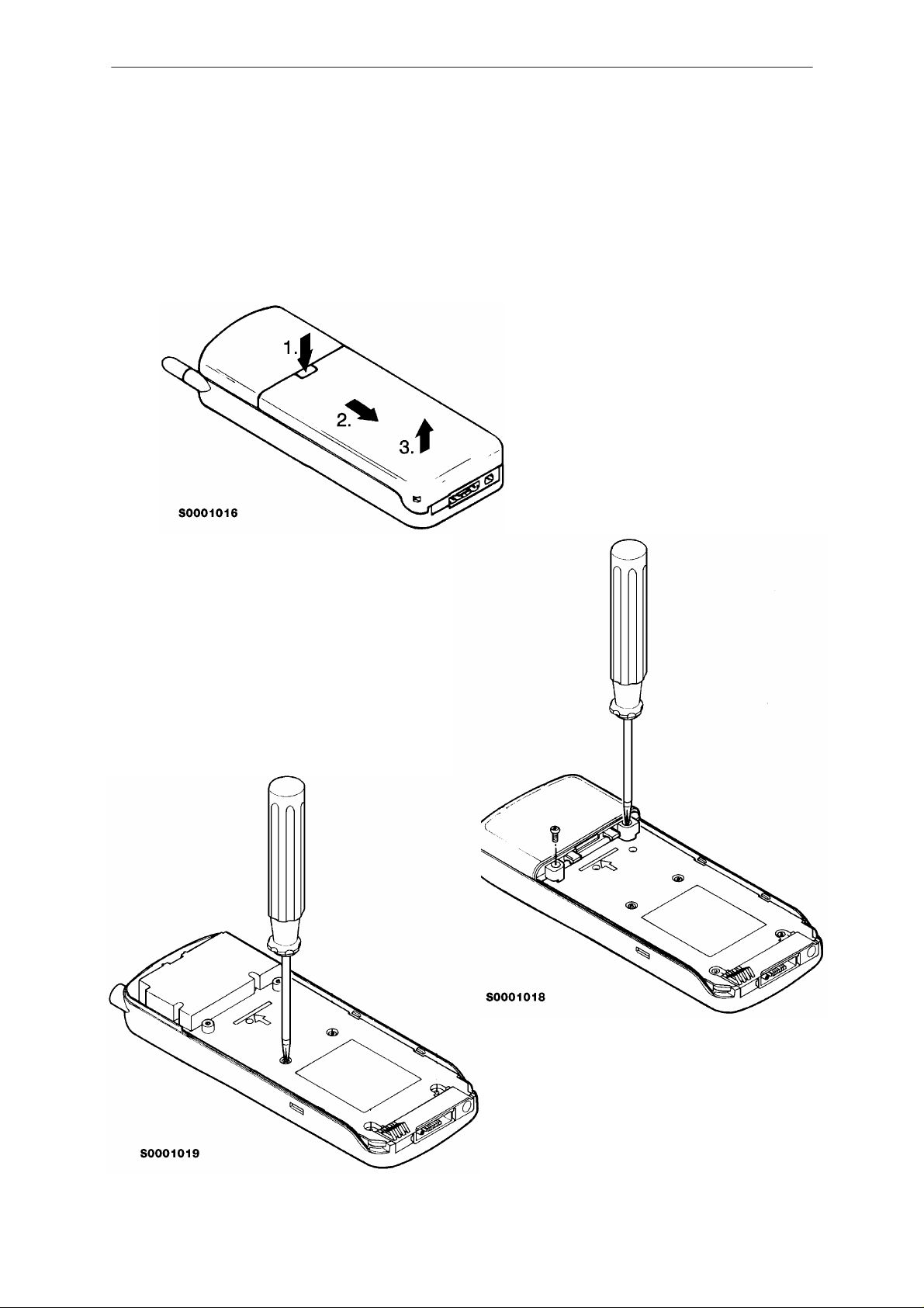
Disassembly Instructions
Disassembly & Troubleshooting
Remove the battery.
Now remove two back
cover screws and remove the back cover
by lifting it away.
2
1
4
3
6
Then remove six
chassis screws.
Issue 1 04/99
5
Page 5
Page 6
NHP–4
PAMS
Disassembly & Troubleshooting
Technical Documentation
Remove the chassis by lifting.
Turn around the chassis and open
the display module a little.
Open the display module connector
by pressing both sides of connector
and slide off the display module
cable.
Page 6
Issue 1 04/99
Page 7
PAMS
NHP–4
Technical Documentation
Turn chassis again and remove
four chassis screws.
Disassembly & Troubleshooting
1
4
3
2
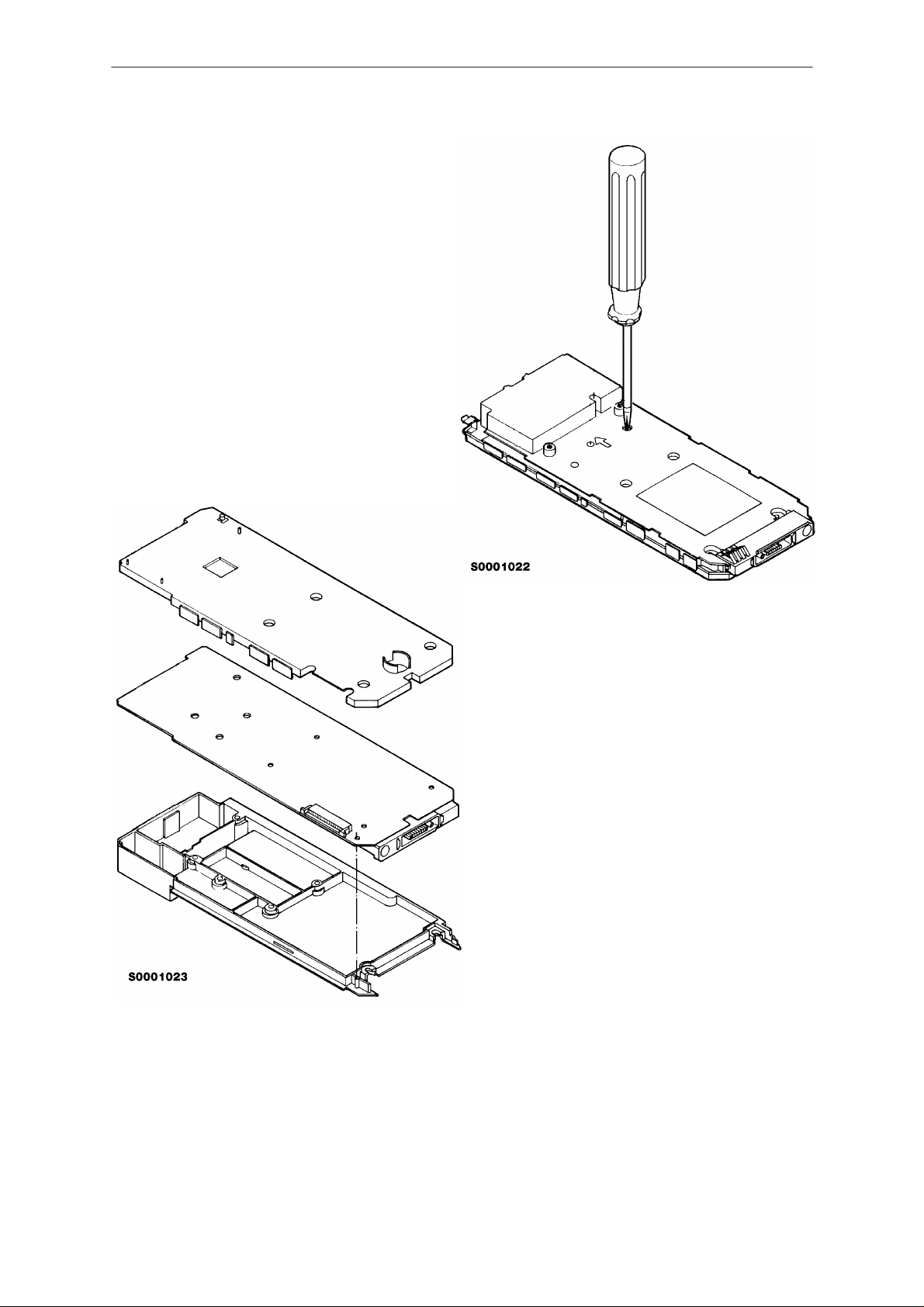
Remove the plastic shield and
throw it away (it is disposable).
Now you can separate the sys-
tem module from the bottom
shield by lifting it away.
Issue 1 04/99
Page 7
Page 8

NHP–4
PAMS
Disassembly & Troubleshooting
HD891 Baseband Troubleshooting
Overview of baseband troubleshooting
Baseband oriented failures are typically discovered during flash and
alignment. Before programming the flash memory, the phone is started in
minimum mode and current consumption is measured. If current
consumption is within acceptable limits and the MCU software version is
successfully read via MBUS, the flash is then programmed. If flash
programming fails, the phone is taken off line where MCU self tests will be
performed at a separate troubleshooting station. During MCU self tests,
address and data lines to the major components of the baseband are
tested. Each test returns the number of the test and the results ( OK /
failed ). Test information is also stored to a phone test file, which can be
available for later use.
If the phone can be flashed and the DSP downloaded, the baseband is
generally functioning properly. If not, referring to the test file of the phone
will aid in the detection of defective components or connections.
Technical Documentation
General
In case of current consumption/MBUS registration failure, more specific
measurements of voltages, clocking signals and states of reset signals
must be evaluated.
The purpose of this document is to define a method by which failures in
the baseband of the phone can be detected and corrected. Each section
of the circuit shall be described in adequate detail such that the reader
may be able to verify whether each section is functioning properly, and if
not, where the problem resides.
Required servicing equipment:
1Service software
1Power supply (1.0 A)
1Digital multimeter
1Oscilloscope
1Modular cable
1RS232/MBUS adapter
1Soldering iron and related tools.
General Failures
The most common baseband failures detected in production will likely be
the following:
1) The phone will not flash (phone seems dead).
2) The DSP will not download.
3) Phone will power up in minimum mode and then power down.
Page 8
Issue 1 04/99
Page 9

PAMS
NHP–4
Technical Documentation
Other Possible Failures
Less likely failures may be:
1) Power circuit
2) Reset logic
3) Clocks
4) Charging circuit
5) BTEMP
6) BTYPE
7) Power to differential audio circuit and headset (VAHS)
8) RFTEMP
9) Watchdog circuit
Troubleshooting Specific Sections
Below describes in detail each of the main circuit sections. Circuit
verification and troubleshooting can be performed by verifying the signals
and voltages described in each section.
Disassembly & Troubleshooting
Power
3 Volt Switching Power Supply
The MAX887 (N704) is the 3V power supply for the baseband. Pin 8
should have battery power at all times (unless, of course, the battery is not
installed), and pin 7 is the output which is approximately 3.15V. This
output by nature will be very noisy. However, it is filtered by an LC circuit
and a rectifying diode which gives a fairly clean supply. This should be
evident by probing the signal labeled 3VD.
Pin 1 is the control pin for the power supply. The supply is active when
this pin is at a logic high (in this case 2.5V), and powers down when it is at
a logic low. It is connected directly to the watchdog circuit, which controls
whether the power supply is on or off.
Pin 6 is the sync pin, which allows the supply to switch in sync with the
clock driving it. The clock frequency should be 307kHz, but should still
function with no clock at all.
3V Power Distribution
Check the MCU (D706) supply voltage 3VD (3.15V) on pins 5 and 42, and
VREF (3.15V) pin 60. Check voltages of MCU related memory
components: FLASH (D702) pins 30, 31 and 11; RAM (D708) pin 7; and
EEPROM (D703) pin 8.
Check the ASIC (D705) supply voltage 3VD (3.15V) on pins 13, 22, 27,
44, 60, 65, 74, 88,103, 109, 117, 132, 146, 151, 161, and 176.
Issue 1 04/99
Page 9
Page 10

NHP–4
PAMS
Disassembly & Troubleshooting
Check the,DSP (D707) supply voltage 3VD (3.15V) on pins 8, 11, 36, 39,
49, 64, 76, 87 and 90. 3VD (3.15V) is also fed to the DSP RAM (D709) to
pin 11 and 33.
Check the CDRFI (N703) supply voltage 3VD (3.15V) on pins 32, 33, 60,
62, 2, 6, 8 and 19.
Check the supply voltages of the audio CODEC (N706). 3VA (3.15V) is
fed to pins 41 and 42. 3VD (3.15V) is connected to pin 18.
4.8 Volt Linear Regulator
The 4.8 volt linear regulator (N707) supplies power the the flex circuit
board (UIF), the differential audio circuit at the output of the CODEC and
leading to the bottom connector, and the headset accessory.
Pin 6 is the power input to the regulator and should be connected to
battery voltage. Pin 1 is an on/off switch. When this pin is high the
regulator is on, and when low it is off. The output is at pin 4 and is labeled
5VD.
Technical Documentation
Reset Logic
XPWR_RESET is the main reset for the entire baseband. It is generated
at pin 7 of N705 and is associated with a RC delay at pins 1 and 5 to give
the circuit time to power up before letting the reset go inactive. With the
battery installed, pins 2 and 6 of N705 must always be at 2.5 volts (these
pins are connected to the 2.5 volt reference diode).
XPWR_RESET drives only the CDSB ASIC at pin 2. When the ASIC is
fully active it then drives the reset (XSYS_RESET, pin 168) to the MCU
(pin 10) and the DSP (pin 69). This reset is asserted whenever the
battery is plugged in, or when the power–on button is pressed. All resets
are active low. When the phone is up and running, all resets should be
high.
Clocks
The MCU (D700), DSP(D707), and ASIC(D705) must all have an active
clock driving them in order to function. The clocks are fundamentally
derived from the VCTCXO (G100) in the RF section. It emits a 15.36MHz
sinusoid which drives the CDRFI (N703, pin 1). The same RF section
also emits a 9.83MHz sinusoid which drives the CDRFI at pin 3. These
signals MUST be present in order for the phone to function.
Page 10
The CDRFI then generates the squarewave version of these two
sinusoids and sends them to the ASIC (15.36MHz at pin147 and 9.83MHz
at pin162).
Pin 104 of the ASIC drives the MCU clock (MCU_CLK) at MCU pin 69,
and drives the DSP clock (DSP_CLK) at DSP pin 68.
Issue 1 04/99
Page 11

PAMS
NHP–4
Technical Documentation
Watchdog
The watchdog circuit is used to monitor whether the MCU software is
functioning properly. The watchdog circuit will shut down the phone if it is
not updated regularly by the MCU. Currently, the watchdog will expire and
shut down the phone 9 seconds after the power–on button is pressed.
Therefore, if the MCU fails to begin resetting the watchdog before the 9
seconds has elapsed, the phone will be shut down.
The MCU software is written such that it resets the watchdog once every
2.5 seconds. If the phone remains on (hence, the watchdog is being
updated), it is believed that the MCU software is functioning properly.
The MCU drives the watchdog pulse from pin 43. It is active high. The
signal drives an inverter (D701) which then drives the watchdog circuit.
By probing the MCU pin and pin 4 of D701, the watchdog pulse can be
verified. An AC version of this pulse can be seen at pin 3 of comparator
N702. Pins 2 and 5 of N702 should always be at 2.5V.
Disassembly & Troubleshooting
The behavior of the RC delay can be monitored at pin 1 of N702. The
voltage at this pin should rise slowly, and then instantly drop to a low
voltage. It will slowly rise again and repeat the process. The signal will
drop in conjunction with watchdog pulse. If the voltage rises above 2.5
volts, pin 7 of N702 will go low and shut down the 3V power supply.
The watchdog can be reset by the MCU pulse (as mentioned above) OR
when the power–on button is pressed (XPWRON), or when the battery is
plugged in, or when a charger is plugged in.
Charging Circuit
The charging circuit is used to control the current transfer from the
charger to the battery. When the CHAR_PWM signal from pin 76 of the
MCU is high, current is flowing from the charger to the battery via V705.
When this signal is low, charging is stopped. When a battery becomes
fully charged, CHAR_PWM will pulse 2 times per second to maintain
battery voltage. The MCU detects when a charger is plugged in when the
CHAR_INT signal goes high (3V). This signal interrupts the ASIC, which
then interrupts the MCU. The charger voltage is approximately 12V when
CHAR_PWM is low, and about 7.5 to 8.5V when it is high.
The MCU monitors the battery voltage through the BATT_ADC signal.
This signal should be approximately 1/3 of the actual battery voltage.
The MCU monitors the charger voltage through the CHAR_ADC signal.
This signal should be approximately 1/8 of the actual charger voltage.
MCU
Address and Data Lines
If the phone successfully flashes, then it can generally be concluded that
the MCU if functioning properly. If it does not flash, the phone must be
Issue 1 04/99
Page 11
Page 12

NHP–4
PAMS
Disassembly & Troubleshooting
further tested to determine whether the address and data lines are
connected and functioning properly by performing read and write cycles to
various parts of the phone. This will be done at a separate test station.
MBUS
If the MBUS line is not working, the phone can not be flashed. MBUS
signals must appear at MCU pins 66 (TXD) and 67 (RXD). For TXD they
must also appear at pin 2 of V711 and pin 2 of V712. For RXD the signals
must appear at pins 1 and 4 of D706.
BTEMP, BTYPE, RFTEMP1, RFTEMP2, VAHS
The circuits for BTEMP and BTYPE can be verified by checking whether
the components are connected as described in the schematic. In MCU
inputs for these signals are on pins 55 and 57, respectively, and should
maintain a constant DC value. If either of these are not functioning
properly, it may be that the components were placed incorrectly, or messy
solder has shorted out some of the components.
Technical Documentation
RFTEMP1 and RFTEMP2 are multiplexed into one MCU pin (56). The
switch (D704) is controlled by MCU pins 44 and 45. When one of these
pins goes high, the corresponding switch is closed, resulting in a short
circuit from the input to the output. This can be verified by monitoring the
input and output of a switch with a voltmeter, and observing that the input
voltage is equal to the output voltage
VAHS is turned on by MCU pin 74 via V710 and V715. It should be about
4.7V when on, and high impedance when off.
DSP
CODEC & Differential Amplifier
The CODEC (N706) is the audio interface to the user. It has two main
clocks, MCLK and CCLK. MCLK must be continuously on during linear
speech coding or decoding. CCLK is used to clock serial data to the
control registers.
The main microphone (hand portable mode) drives pins 33 and 34. The
external microphone (XMIC) is used for accessories only, and drives pin
31.
Page 12
The earpiece (internal speaker) in driven differentially by pins 5 and 6.
Receive audio for the accessories is driven from pins 2 and 3 into a
differential amplifier. This circuit is different from the usual
accessory/CODEC design. The opamp (N708) is powered by VAHS
which is switched on by the MCU when an accessory is detected.
Pin 5 must be at 4.7V. Pin 4 must have a DC value of about 2.5V, and the
hot node of the 2.5 volt shunt regulator must also be at 2.5V.
Issue 1 04/99
Page 13

PAMS
NHP–4
Technical Documentation
Failures
Current consumption failures
Usually common to these types of failures is that phone can not be
programmed or tested via MBUS. The most common failure is that phone
takes normal current during startup and after a few seconds all circuits
are powered down. The reason for this failure could be in power, clock or
reset distribution of the phone. In cases where the phone does not take
current at all, or the phone takes all available current, the reason is usually
a defective 3V power supply (N704) or bad soldering (short or open)
around it.
Phone takes all available current
If phone takes all available current, the problem is likely caused by a
shorted component. Verify correct operation of the 3V power supply
(N704). Check solder joints, and the components around it and bottom
connector (X700).
Disassembly & Troubleshooting
Phone does not take current at all
If phone does not take current at all, verify correct operation of the 3V
power supply (N704). If pin 1 is always being held low, check the
watchdog circuit for proper operation.
Current consumption OK during power–up, then fail
A more common failure in current consumption is that the phone seems to
start normally, then after few seconds all circuits are powered down. The
power–down is likely caused by the absence of the MCU watchdog pulse.
Verify that the 3V power distribution to all baseband main components is
correct. Then check that the clocks are operating. If everything seems
OK, check that the RESET logic is operating properly.
Issue 1 04/99
Page 13
Page 14

NHP–4
PAMS
Disassembly & Troubleshooting
Technical Documentation
Troubleshooting Diagram; Flash Programming OK, part 1
FLASH programming OK
MBUS
registration
OK?
NO
YES
Does LCD
display turns
ON?
YES
NO
Check D706 pins 3,80
ASIC pins 130,86
3
Short circuits in data
data lines. data line
disconnected, VREF
disconnected
Check that pin 4 of D500
NO
is 4.75V. Also check the
control line, it should be
high (3V on Pin 1 of
Check X701
C507 OK?
YES
Power
stays on?
NO
NO
NO
N500 pin 8/XRESET
VBATT
N500 pin 5,20
?
YES
3V after power ON?
YES
display turns
YES
MBUS line X701
pin 5, Is 4.75V after
YES
Does LCD
ON?
pwr ON?
NO
D500).
R500, R503
OK?
YES
Change N500
YES
Power supp. to the logic
circuits +3V after power
ON?
NO
Change N500
D706 pin 67
+3V after power ON?
NO
YES
2
YES
Change D706
Check V703,
R728, R726,
R727, if OK
change D706
Page 14
Issue 1 04/99
Page 15

PAMS
NHP–4
Technical Documentation
Disassembly & Troubleshooting
Troubleshooting Diagram; Flash Programming OK, part 2
2
NO
Check D704 and D706 for
short/open pins, if pins look
OK change D704 if problem
continues change D706
D706 pin 10
XSYS_RESET +3V after
power on?
YES
15.36MHz at
D706 pin 69
?
YES
D706 pin8/MD2
and pin9/STBY are
+3V ?
YES
NO
NO
Check clock
signal in N700
and D704
Check these
two pins for
shorts and
opens
D706 pin 43/
XPWROFF has 0V to +3V
pulses after power
ON ?
YES
D706 pin 77
/IRQ0 +3V after
power on?
YES
D706 pin 11
/NMI 0V after
power on?
YES
D706 pin 4
/XMCU_WR +3V
after pwr on?
NO
Change D706
Check D704 and
NO
D706 for shorts
and opens. If OK
change D706
Check D704 and
NO
D706 for shorts
and opens. If OK
change D706
NO
Check D706
Issue 1 04/99
YES
Check all soldered joints
The data and address signals must have
a clear difference between low (0 V)
and high (+3V)
Page 15
Page 16

NHP–4
PAMS
Disassembly & Troubleshooting
Technical Documentation
Troubleshooting Diagram; Flash Programming OK, part 3
3
MBUS registration OK?
YES
Does LCD display turns ON ?
YES
Check D706
and D703
interface
NO
D703 initialization
(Factory Values Set) OK?
NO
D703
pin 18,19/D0,D1
+3V to 0V during r/w
operations ?
YES
Change D703
YES
4
Page 16
Issue 1 04/99
Page 17

PAMS
NHP–4
Technical Documentation
Disassembly & Troubleshooting
Troubleshooting Diagram; Flash Programming OK, part 4
4
D709
/pin 11 is 12V while
programming?
YES
D706
/pin 64/HOOK_RXD2
pulses during prog?
YES
NO
NO
Check X701/pin14
L700,C729,R748
R741
Check X701 pin 6
R736,R739,R764
C723
X701 pin 7
/PHFS_TXD2 pulses
during programming?
YES
D709
pin 10/RP +3V after
power ON ?
YES
D709
pin 22/CE pulses
from +3V to 0V after
power ON?
YES
D709
pin 24/OE pulses
from +3V to 0V after
power ON ?
YES
NO
NO
NO
NO
Check D706 pin 63
R725,R735,C721
Check VCO_EN line
at the D709 pin 10 for
shorts and opens
Check XFLASH_CS
line at theD704 pin 107
Check XMCU_RD line
at the D706 pin 3
Check D709 address and
data lines for shortcircuits
or unconnected pins
OK
Change D709
Issue 1 04/99
YES
D709
pin 9/WE pulses
from +3V to 0V after
power ON ?
NO
Check XMCU_WR line
at the D706 pin 4
Page 17
Page 18

NHP–4
PAMS
Disassembly & Troubleshooting
Troubleshooting Diagram; PWR Button Fault
Nothing happens when
PWR button is pressed
N500
pin 10 +3V when
VBATT is connected?
YES
NO
Technical Documentation
Check
X701
NO
N500 pins 5,20
VBATT voltage?
YES
Change
N500
Check
UI–conn. X700
Change
UI
NO
pin 10 goes low when
N500
PWR button is
pressed?
YES
R500,R503
C507 OK
Check component
around N500, if OK
change N500
Page 18
Issue 1 04/99
Page 19

PAMS
NHP–4
Technical Documentation
Troubleshooting Diagram; Audio Fault
Audio fault
Microphone or earphone
signal missing
N600 pin 19/CODEC_FS from D704
Microphone and
earphone signal
missing?
NO
YES
N600 pin 20/CODEC_MCLK from D704
D705 pins 29,37/CODEC_FS from D704
D705 pins 27,33/CODEC_MCLK from D704
Disassembly & Troubleshooting
Microphone signal
missing?
NO
Earphone signal
missing?
YES
YES
N600 pin 25,24/MICP,MICN
N600 pin 17/PCMOUT
N600 pin 21/MICENX
corresponding pins of UI–connector
N600 pin 7,8/EARP,EARN
N600 pin 10/PCMIN
corresponding pins of UI–connector
Issue 1 04/99
Page 19
Page 20

NHP–4
PAMS
Disassembly & Troubleshooting
Power Up Sequence Diagram
VBAT 5.3....8V
CHRGDET
DETIN
ON
CDCONT
N201
5, 20
11
12
14
XPWROFF
C507
23
N500
9
13
VRXS 4.5V
VCO_EN
VL1 MCU_CLK (15.36MHz)
4
VL2
21
VL3
16
VA1
2
VA2
24
XRESET
82
VREF
1
VCTCXO
G300
CLK 15.36MHz
1
CDRFI N700
63
CLK 15.36MHz
128
147
104
168
ASIC MCUPSL
121
98
D704
Technical Documentation
Square circuitry
XSYS_RESET (3.15V)
MCU_INT0 (3.15V)
MCU_NMI (0V)
ON=3.15V
69
10
77
11
5,42
D706
43
66
TXD
XPWROFF 7s
PSL_+3V(N500)
1Output voltages must stay high at least 7seconds when power is
switched on.
1If no; check C507.
1If it is OK; replace PSL_+3V(N500).
1If the XRESET line doesn’t rise check DETIN. The voltage value at this
pin should be between 1.46V and 1.72V.
ASIC(D704)
1When XRESET and CLK are supplied to the ASIC(D704) but MCUCLK
or XSYS_RESET to the MCU(D706) are not supplied; replace
ASIC(D704).
MCU(D706)
1If MCU_CLK and XSYS_RESET are supplied from ASIC(D704) but TXD
line (MBUS) doesn’t rise and solder joints of the MCU(D706) are good,
check that MCU_INT0 is high (3.15V) and MCU_NMI is low (0V), if
that is the case then replace MCU(D706).
Page 20
1If TXD pin 66 of the MCU(D706) goes high but doesn’t stay there at
least 7seconds.
The power of the phone can be kept ON by:
Connecting PSL +(N500) pin 14 to the ground.
Now it is possible to use service software for troubleshooting.
Issue 1 04/99
Page 21

PAMS
NHP–4
Technical Documentation
Disassembly & Troubleshooting
Repairing Instructions for Flash Faulty Units
1. When the phone doesn’t start (power off after 7seconds and probably no MBUS
connection) check following things:
1VBATT is connected to the PSL_+3V(N500)
1XRESET rises to 3.15V
1VL1 is 3.15V
132KHz clock is running.
1VRXS(4.5V) is connected to the VCTCXO and the crystal frequency is
15.36 MHz
1XSYS_RESET signal rises to 3.15V
1MCU_CLK signal is 15.36 MHz
1MCU_NMI line stays low(0V)
1MCU_IRQ0 line stays high(3.15V)
If all these happens, the MCU(D706) will supply power OFF pulses to the
PSL_+3V(N500) and the power will stay on.
In faulty conditions, most likely MCU_IRQ0 stays low(0V), which means
that interrupt is generated all the time.
In this case check data and address lines of ASIC(D704), MCU(D706)
and memory circuits for short circuits or unconnected pins.
2. When FLASH programming is not succeed, check following things:
1System connector(X701) pins 6, 7, 14 are soldered and there are no
short circuits.
1Flash programming voltage (VF=12V) is connected to the FLASH(D709)
pin 11.
1The data and address lines of the FLASH(D709) are soldered.
1EEPROM(D703) should be OK because of the initialization (program pa-
rameters are loaded always when program is loading the first time).
3. When FACTORY SET is not succeed or the power is switched off after
programming:
When power is switched on the program of the phone will go to maximum
mode and if this doesn’t work, there was a problem during the flash
programming.
1Check solder joints of EEPROM(D703).
1Do FACTORY SET once again.
Issue 1 04/99
Page 21
Page 22

NHP–4
PAMS
Disassembly & Troubleshooting
Calibrate Battery Voltage (VBATDET)= 6.0V
a) Check R505, R504
b) Check PSL_+3V(N500) pin 23
c) Check MCU(D706) pin 52
Calibrate Charge Voltage (VC)= 6.0V
a) Check R502, R501, R508
b) Check MCU(D706) pin 53
Technical Documentation
Page 22
Issue 1 04/99
Page 23

PAMS
NHP–4
Technical Documentation
Disassembly & Troubleshooting
Troubleshooting Diagram; Power Up and MCU Self tests Malfunctions
RADIO UNIT CHECK
Press power on
Current
consumption
OK?
YES
NO
See Power Up
Malfunction
Run self tests
OK?
YES
Call process
Audio check
OK
NO
See Self Tests
Malfunction
Issue 1 04/99
Page 23
Page 24

NHP–4
PAMS
Disassembly & Troubleshooting
Power Up Malfunction
Basically there are two different problems that could occur while powering
up the phone. First, the current consumption is almost zero all the time.
Probably the fault is at the power circuit PSL_+3V(N500). Check all
PSL_+3V(N500) connections including VBATT line.
Second, the phone’s current consumption is normal for 7seconds and
goes to zero after that time. The reason for this is the watchdog.
1.0 Is MCU’s clock running?
1Check with oscilloscope if there is a clock signal at MCU(D706) pin 69. It
should be a square wave signal, 50% duty cycle, 3Vpp and 15.36MHz.
See Figure 1. Is the clock running?
Technical Documentation
Page 24
Figure 1
1YES! Go to 2.0 / NO! Go to 1.1
1.1 Is VCTCXO running?
Measure CDRFI(N700) pin 1. See Figure 2. Is there a
15.36MHz sine wave signal?
Issue 1 04/99
Page 25

PAMS
NHP–4
Technical Documentation
Disassembly & Troubleshooting
Figure 2
YES! Go to 1.2 / NO! Go to 1.11
1.11 Check VCO_EN is high (3.15V)
CDCONT(N201) pin 23.
1.12 Check VCTCXO(G300) waveform at
CDCONT(N201) pin 35 looks like Figure 3. Also check that
VRXS line is 4.5Vdc at CDCONT(N201) pin 13. If all these
conditions are meet check solder joints for shorts and opens, if
they are OK replace CDCONT(N201).
Figure 3
Issue 1 04/99
Page 25
Page 26

NHP–4
PAMS
Disassembly & Troubleshooting
1.2 Check CDRFI(N700) pin 63. See Figure 4. Is there a
15.36MHz clock signal present?
Technical Documentation
Figure 4
YES! Go to 1.22 / NO! GO to 1.21
1.21 Check this signal solder joints, if OK replace
CDRFI(N600).
1.22 Check connections between ASIC(D704) and
MCU (D706), especially ASIC(D704) pin 104 and MCU(D706)
pin 69. If no clock is present and connection looks OK replace
ASIC(D704).
2.0 Are MCU’s supply voltages OK?
1Measure MCU(D706) supply voltages from pins 5 and 42 (nominal 3.15V
Vdc ±0.15 Vdc). Are supply voltages right?
1YES! Go to 3.0 / NO! Go to 2.1
2.1 Check PSL_+3V(N500) VL1(3.15V) pin 4
3.0 Is XSYS_RESET signal OK?
1Check XSYS_RESET at MCU(D706) pin 10. While a high (about 3.15
Vdc) is ok, GO to 4.0. If zero then MCU(D706) is in reset, GO to 3.1.
3.1 Is XPWR_RESET signal from PSL_+3V(N500) OK?
Page 26
Check XPWR_RESET line from PSL_+3V(N500) pin 8. If it
is high GO to 3.12, if zero GO to 3.11.
3.11 Check PSL_+3V pin 12. Voltage should be between 1.46V
and 1.72V. if not check R500, R503 and VBATT voltage(5.3...8
)
NOTICE! Measure pin 10 from the PSL_+3V(N500) with
V
dc
oscilloscope. That is watchdog signal coming from
Issue 1 04/99
Page 27

PAMS
NHP–4
Technical Documentation
MCU(D706). There should be rising edges time to time.
these are OK and still XPWR_RESET is low replace the
PSL_+3V(N500).
3.12 Check reset line for shorts and open between MCU(D706)
and ASIC(D704), and between PSL_+3V(500) and
ASIC(D704). If OK replace ASIC(D704).
4.0 Is 32KHz clock running?
1Check with oscilloscope if there is a 32.768KHz clock signal at
ASIC(D704) pin 87. It should look like Figure 5.
Disassembly & Troubleshooting
If all
Figure 5
1YES! Go to 5.0 / NO! Go to 4.1
5.0 Check all supply voltages!
1Measure all power supply voltage lines VL1(3.15V), VL2(3.15V),
1Are voltages right? YES! Go to 6.0. / NO! Read ahead!
1If any voltage is not the right one, check corresponding transistor. VL1
1Check also all major circuits supply voltages MCU(D706), ASIC(D704),
Issue 1 04/99
4.1 Check solder joints in ASIC(D704) pins 36, 37, 46, 125.
Also check B700, C744, C745, R837, R757, If they are OK replace B700. If problem persists replace ASIC(D704).
VL3(3.15V), VA2(3.15V) and VREF(3.15V).
(V500), VL2(V502) and VL3(V501).
PSL_+3V(N500), DSP(D705), CDRFI(N700) and CODEC(N600).
Page 27
Page 28

NHP–4
PAMS
Disassembly & Troubleshooting
1This table might help to locate power pins on main circuits.
Circuit Number Pins Supply voltage signal
MCU D706 5,42 VL1
ASIC D704 13,22,27,44,60,65,74,88,103 VL1
D704 109,117,132,146,151,161,176 VL1
DSP D705 8,11,36,39,49,64,76,87,90 VL2
CDRFI N700 32,33,60,62,2,6,8,19 VL3
CODEC N600 2,3 VA2
N600 15 VL1
FLASH D709 30,31,11 VL1
RAM D700 28 VL1
EEPROM D703 7 VL1
6.0 FLASH–line OK?
Power up function OK!
1YES! Power up function OK! / NO! Do flashing again.
Technical Documentation
Page 28
Issue 1 04/99
Page 29

PAMS
NHP–4
Technical Documentation
Disassembly & Troubleshooting
Troubleshooting Diagram; Power Up Malfunction
Start
1.11 Check
VCO_EN is 3V
1.12 Check
Vctcxo sine wave
and VRXS is
4.5V, if OK
replace CDCONT
(N201)
Check solder
joints, if OK
replace
CDRFI
(N700)
NO
1.1 VCTCXO
running OK?
YES
NO
1.2 Clock signal
at CDRFI (N700)
pin 63 ?
YES
1.22 Check connections
between D706 and D704
especially clock signals.
If they are OK replace
D704
NO
1. MCU
clock running
OK?
YES
2. MCU’s
supply voltages
OK?
YES
3. MCU
reset signal OK?
YES
NO
NO
2.1 Check PSL+(N500)
VL1–line at pin 4
3.1 Is N500
XPWR_RESET signal
OK?
YES
3.12 Check connections
between D706, D704 and
N500. If OK replace D704
NO
3.11 Check
PSL+(N500)
pins 10
and 12
if OK replace
PSL+(N500)
Power up
Issue 1 04/99
Check
corresponding
component
OK!
YES
NO
4. Is 32KHz
clock running
OK ?
YES
5. All supply
voltages OK?
YES
6. FLASH line
OK?
NO
NO
4.1 Check D704 pins 36,
37,46,125. Also check
B700, C744, C745, R837.,
R757. If they are OK
replace B700. If problem
persists replace D704
Do flashing again
Page 29
Page 30

NHP–4
PAMS
Disassembly & Troubleshooting
Important Information
This section contains information that might be helpful while
troubleshooting an HD881 phone. However it is not needed to
troubleshoot power up problems.
9.8304MHz clock
This clock is ”ON” when the phone is set to CDMA non–slotted mode and
it is ”OFF” when the phone is set to AMPS mode. It is generated inside the
CDCONT(N201) from the 15.36MHz. The waveform signal coming out
from the CDCONT(N201) pin 40 should look like Figure 6.
Technical Documentation
Page 30
Figure 6
Then this signal is fed to the CDRFI(N700) squaring circuit on pin 3 to get
the final 9.8304MHz clock signal that will go to the ASIC(D704). This clock
should look like Figure 7.
Issue 1 04/99
Page 31

PAMS
NHP–4
Technical Documentation
Disassembly & Troubleshooting
Figure 7
Issue 1 04/99
Page 31
Page 32

NHP–4
PAMS
Disassembly & Troubleshooting
[This page intentionally left blank]
Technical Documentation
Page 32
Issue 1 04/99
 Loading...