

Page 1

Programme’s After Market Services
NHP–4 Series Transceivers
Chapter 4
System Module
Issue 1 04/99
Page 2

NHP–4
System Module
Technical Documentation
Contents
Baseband Block 4–5. . . . . . . . . . . . . . . . . . . . . . . . . . . . . . . . . . . . . . . . . . . . . . . . . .
Baseband Block Connections 4–5. . . . . . . . . . . . . . . . . . . . . . . . . . . . . . . . . . .
Internal Signals and Connections 4–6. . . . . . . . . . . . . . . . . . . . . . . . . . . . . . . .
Functional Description 4–13. . . . . . . . . . . . . . . . . . . . . . . . . . . . . . . . . . . . . . . . . . . .
Power Management 4–14. . . . . . . . . . . . . . . . . . . . . . . . . . . . . . . . . . . . . . . . . . .
MCU BLOCK 4–16. . . . . . . . . . . . . . . . . . . . . . . . . . . . . . . . . . . . . . . . . . . . . . . . .
DSP Block 4–18. . . . . . . . . . . . . . . . . . . . . . . . . . . . . . . . . . . . . . . . . . . . . . . . . . .
Digital ASIC Clock 4–20. . . . . . . . . . . . . . . . . . . . . . . . . . . . . . . . . . . . . . . . . . . . .
CDRFI 4–21. . . . . . . . . . . . . . . . . . . . . . . . . . . . . . . . . . . . . . . . . . . . . . . . . . . . . . .
Audio Block 4–22. . . . . . . . . . . . . . . . . . . . . . . . . . . . . . . . . . . . . . . . . . . . . . . . . .
PAMS
Page No
RF Block Introduction 4–23. . . . . . . . . . . . . . . . . . . . . . . . . . . . . . . . . . . . . . . . . . . . .
Transmitter 4–23. . . . . . . . . . . . . . . . . . . . . . . . . . . . . . . . . . . . . . . . . . . . . . . . . . . . . .
Functional Description 4–23. . . . . . . . . . . . . . . . . . . . . . . . . . . . . . . . . . . . . . . . .
Circuit Description 4–27. . . . . . . . . . . . . . . . . . . . . . . . . . . . . . . . . . . . . . . . . . . . .
Receiver 4–33. . . . . . . . . . . . . . . . . . . . . . . . . . . . . . . . . . . . . . . . . . . . . . . . . . . . . . . .
Functional Description 4–33. . . . . . . . . . . . . . . . . . . . . . . . . . . . . . . . . . . . . . . . .
Synthesizer 4–38. . . . . . . . . . . . . . . . . . . . . . . . . . . . . . . . . . . . . . . . . . . . . . . . . . . . . .
The VCTCXO Clock (G100) 4–38. . . . . . . . . . . . . . . . . . . . . . . . . . . . . . . . . . . .
The Fujitsu Dual PLL Frequency Synthesizer IC (N101) 4–38. . . . . . . . . . . .
The 2 GHz UHF Channel Selector (LO_PRX, LO_PTX) 4–39. . . . . . . . . . . .
The 416.2 MHz TX VHF LO (LO_TIF) 4–39. . . . . . . . . . . . . . . . . . . . . . . . . . . .
The 256.2 MHz RX VHF LO (LO_RIF)/ 4–40. . . . . . . . . . . . . . . . . . . . . . . . . . .
Motorola MC145162D PLL IC (CLOCKS, N102) 4–40. . . . . . . . . . . . . . . . . . .
Parts List GR2 4–42. . . . . . . . . . . . . . . . . . . . . . . . . . . . . . . . . . . . . . . . . . . . . . . . . . .
Page 4–2
Issue 1 04/99
Page 3

PAMS
NHP–4
Technical Documentation
List Of Figures
Figure 1 Baseband – Interconnections 4–5. . . . . . . . . . . . . . . . . . . . . . . . . . . . .
Figure 2 4–14. . . . . . . . . . . . . . . . . . . . . . . . . . . . . . . . . . . . . . . . . . . . . . . . . . . . . . .
Figure 3 Memory Map 4–17. . . . . . . . . . . . . . . . . . . . . . . . . . . . . . . . . . . . . . . . . . .
Figure 4 DSP memory configuration w/ 64k external SRAM 4–19. . . . . . . . . .
RF/BB Block Diagram 4–A1. . . . . . . . . . . . . . . . . . . . . . . . . . . . . . . . . . . . . . . . . . . .
Power Supply 4–A2. . . . . . . . . . . . . . . . . . . . . . . . . . . . . . . . . . . . . . . . . . . . . . . . . . .
MCU 4–A3. . . . . . . . . . . . . . . . . . . . . . . . . . . . . . . . . . . . . . . . . . . . . . . . . . . . . . . . . . .
MCU Memory 4–A4. . . . . . . . . . . . . . . . . . . . . . . . . . . . . . . . . . . . . . . . . . . . . . . . . . .
DSP 4–A5. . . . . . . . . . . . . . . . . . . . . . . . . . . . . . . . . . . . . . . . . . . . . . . . . . . . . . . . . . .
DSP Memory 4–A6. . . . . . . . . . . . . . . . . . . . . . . . . . . . . . . . . . . . . . . . . . . . . . . . . . . .
RF Block 4–A7. . . . . . . . . . . . . . . . . . . . . . . . . . . . . . . . . . . . . . . . . . . . . . . . . . . . . . .
System Module
Page No
Receiver 4–A8. . . . . . . . . . . . . . . . . . . . . . . . . . . . . . . . . . . . . . . . . . . . . . . . . . . . . . . .
Transmitter 4–A9. . . . . . . . . . . . . . . . . . . . . . . . . . . . . . . . . . . . . . . . . . . . . . . . . . . . . .
Synthesiser 4–A10. . . . . . . . . . . . . . . . . . . . . . . . . . . . . . . . . . . . . . . . . . . . . . . . . . . . . .
Input / Output 4–A11. . . . . . . . . . . . . . . . . . . . . . . . . . . . . . . . . . . . . . . . . . . . . . . . . . .
Clocks 4–A12. . . . . . . . . . . . . . . . . . . . . . . . . . . . . . . . . . . . . . . . . . . . . . . . . . . . . . . . . .
Power 4–A13. . . . . . . . . . . . . . . . . . . . . . . . . . . . . . . . . . . . . . . . . . . . . . . . . . . . . . . . . .
Component Layout – Top 4–A14. . . . . . . . . . . . . . . . . . . . . . . . . . . . . . . . . . . . . . . . . .
Component Layout – Bottom 4–A15. . . . . . . . . . . . . . . . . . . . . . . . . . . . . . . . . . . . . . .
Issue 1 04/99
Page 4–3
Page 4

NHP–4
System Module
PAMS
Technical Documentation
This page intentionally left blank
Page 4–4
Issue 1 04/99
Page 5
PAMS
NHP–4
Technical Documentation
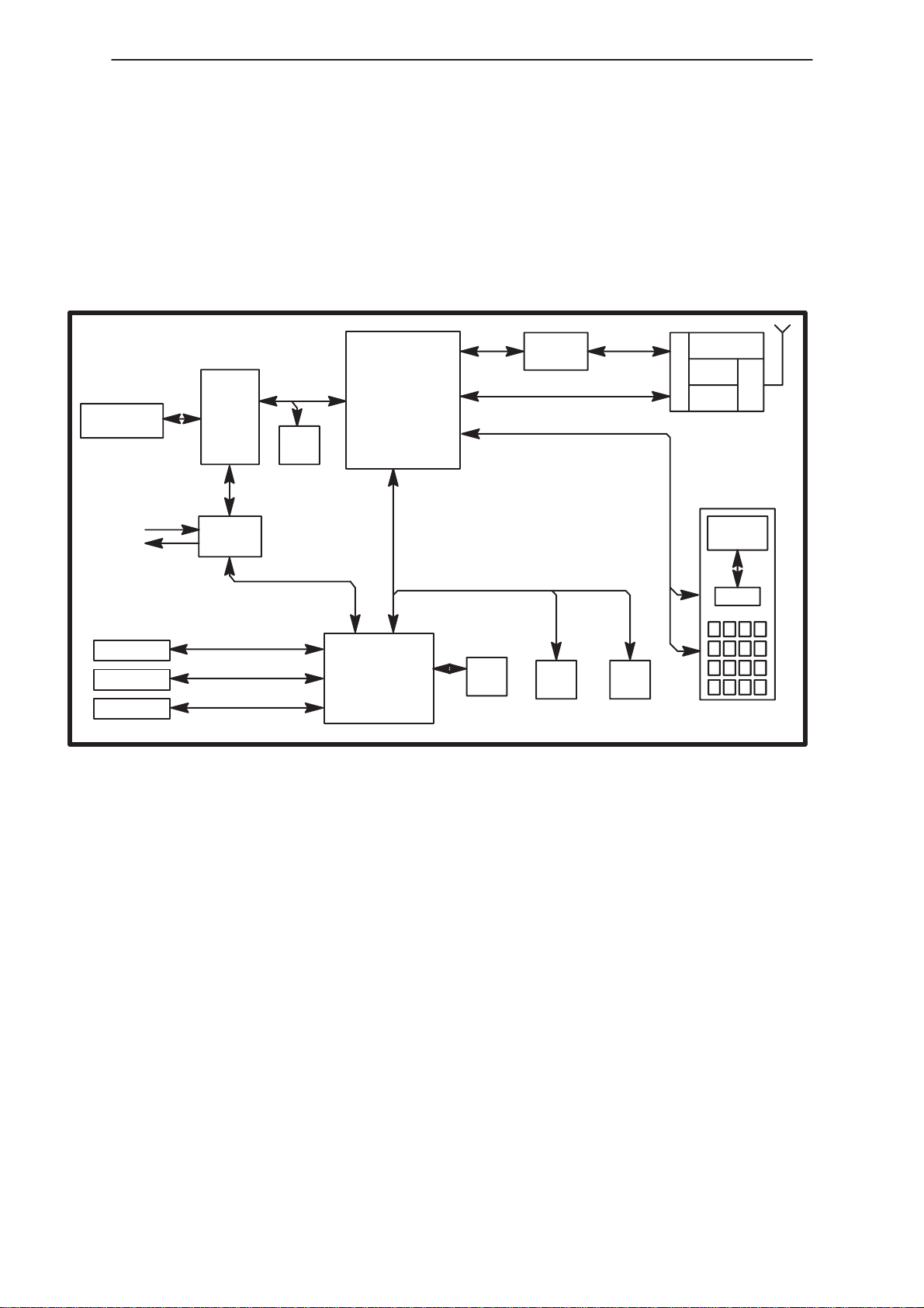
Baseband Block
Baseband architecture refers to all those technology elements in the phone
design which do not include the RF functions. This document describes in
overview, the HD891 baseband architecture. Primarily the focus of this
document will be to highlight those aspects of the baseband architecture which
are unique to the CDMA project.
DSP
DBUS Interface
Multipath Analyzer
Message Injection
IS 125
MIC
EAR
sio
sio
ext
mem
sio
sio
PCM
CODEC
io
A15:0,
D7:0
64K x
16
SRAM
ASIC
CDRFI
System Module
RF
SYN
C
O
N
T
REC
R
O
L
XMIT/MOD
DUP
UIF–module
LCD
io
Switche
r
Charge
FLASH
r
LOAD
MBUS
Interfac
e
Charger Control
sio
sio
io
sio
sio
ext mem
MCU
Figure 1 Baseband – Interconnections
Baseband Block Connections
Below is a list of the functional blocks of the baseband architecture:
– Microcontroller Unit (MCU)
– MCU External Memory –
Electrically Eraseable Programmable Read Only Memory (EEPROM)
Static Random Access Memory (SRAM)
Flash Memory
A19:0,D7:0
sio
16k x 8
Serial
2
PROM
E
1M x 8 32K x 8
FLASH SRAM
LCD Driver
Issue 1 04/99
– Digital Signal Processor (DSP)
– DSP External Memory –
Static Random Access Memory (SRAM)
– CDSB ASIC
– CDMA RF to BB Interface (CDRFI)
– Audio Coder/Decoder (CODEC)
Page 4–5
Page 6

NHP–4
System Module
Technical Documentation
Internal Signals and Connections
Power Block
Table 1. Power Block Connections
Signal Name T ype Notes T o/From
XPWRON IN Power on switch UIF
WATCHDOG IN Watchdog reset pulse MCU
VBATTERY IN Battery voltage Sys. conn.
CHAR+ IN Charger Voltage Sys. conn.
CHAR– IN Charger Return GND
CHAR_PWM IN PWM for controlling battery charging MCU
XPWR_RESET OUT Master reset, Power–on Reset ASIC
3VA OUT Analog 3.15V supply CODEC
PAMS
3VD OUT 3.15V power supply for baseband
5VD OUT 4.8V supply for MBUS and XEAR Differential Circuit
(Switched)
VAHS OUT 4.8V supply for XEAR Differential Circuit (Switched),
and power for the Headset Accessory
LCD_PWR OUT 4.8V supply with series diode and resistor for LCD
(LCD can’t use 4.8V)
BATT_ADC OUT Battery voltage input to ADC MCU
CHAR_ADC OUT Charger voltage input to ADC MCU
CHAR_INT OUT Signal to indicate a Charger has been connected to
Phone.
UIF
Opamp
(N708) and
System Connector
UIF
ASIC
MCU Block
Table 2. MCU Block Connections
Signal Name T ype Notes T o/From
MCU_CLK IN 15.36 MHz Clk into MCU ASIC
XSYS_RESET IN MCU Reset from ASIC ASIC
MCUAD(19:0) OUT MCU 20 bit Address Bus Mem, ASIC
MCUDA(7:0) I/O MCU 8 bit Data Bus Mem, ASIC
XMCU_AS OUT MCU Address Strobe ASIC
XMCU_RD OUT MCU Read used as Output Enable Mem, ASIC
XMCU_WR OUT MCU Write used as Read/Write select Mem, ASIC
MCU_NMI IN MCU Non Maskable Interupt ASIC
MCU_INT0 IN MCU Maskable Interupt 1 ASIC
CODEC_DI OUT
CODEC_CLK OUT
Page 4–6
Audio codec control data MCU
Clock for audio codec control data transfer MCU
Issue 1 04/99
Page 7
PAMS
NHP–4
Technical Documentation
Table 2. MCU Block Connections (continued)
XCODEC_CS OUT
CODEC_DO IN
Audio codec chip select MCU
Audio codec control data MCU
System Module
To/FromNotesTypeSignal Name
CALL_LED OUT UIF CALL_LED enable UIF
BACK_LIGHT OUT UIF BACK_LIGHT enable UIF
PHFS_TXD2 OUT Hands Free speaker Mute Control and Trans-
Sys. conn.
mitted data from Flash during Flash Programming.
HOOK_RXD2 OUT Recieved data during Flash Programming. Sys. conn.
VIB_CONT OUT Vibrator Control for quit alarm Sys. conn.
MBUS_OUT OUT MBUS data output Sys. conn.
VAHS_EN OUT Headset voltage enable Sys. conn.
CHAR_PWM OUT Control PWM for charging batteries. PWR
WATCHDOG OUT Watchdog signal used to reset watchdog cir-
PWR
cuit
TEMP1_EN OUT Control signal to pick RFTEMP1 for A/D read MCU
TEMP2_EN OUT Control signal to pick RFTEMP2 for A/D read MCU
BATT_ADC IN A/D input for battery voltage level PWR
CHAR_ADC IN A/D input for monitoring of charging voltage PWR
HOOK_RXD2 IN A/D input – Hook indicator (Phone on or off
Sys. conn.
Hook)
BTEMP IN A/D input for monitoring Battery temp. Sys. conn.
RFTEMP IN A/D input for monitoring RFTEMP 1 and 2
RF
temp.
BTYPE IN A/D input for monitoring Battery type. Sys.conn.
RSSI IN A/D input for monitoring RSSI. RF
JCONN IN A/D input for monitoring Accessory type. Sys. conn.
MBUS_DET IN MBUS data input. Sys. conn
Issue 1 04/99
Page 4–7
Page 8
NHP–4
System Module
Technical Documentation
PAMS
MCU Memory Block
Table 3. MCU Memory Block Connections
Signal Name T ype Notes T o/From
MCUAD(19:0) IN MCU 20 bit Address Bus MCU
MCUDA(7:0) I/O MCU 8 bit Data Bus MCU
XMCU_RD IN MCU Read used as Output Enable MCU
XMCU_WR IN MCU Write used as Read/Write select MCU
XFLASH_CS IN Flash Chip Select ASIC
XSRAM_CS IN SRAM Chip Select ASIC
VF IN 12 volt line for Flash programming Sys. conn.
DSP Block
Table 4. DSP Block Connections
Signal Name T ype Notes T o/From
DSP_CLK IN 15.36 MHz Clk into DSP ASIC
XSYS_RESET IN DSP Reset from ASIC ASIC
DSP_INT0 IN DSP Maskable Interupt 0 ASIC
DSP_INT1 IN DSP Maskable Interupt 1 ASIC
DSPAD(15:0) OUT DSP 16 bit Address Bus Mem, ASIC
DSPDA(15:0) I/O DSP 16 bit Data Bus Mem, ASIC
DSP_RXW OUT DSP Read / Write Select Mem, ASIC
IO_STRB OUT DSP Master Strobe for Memory Access Mem, ASIC
Codec_FS IN Frame Sync for aligning Codec audio data
ASIC
8KHz
Codec_MCLK IN CLK for moving Codec audio data ASIC
PCMOUT IN Audio Data from Codec CODEC
PCMIN OUT Audio Data to Codec CODEC
DSP_SYNC I/O Frame Sync for aligning data in and out of
DSP. Used by MP, MI, IS125 and Data Acc.
DSP_MCLK I/O CLK for moving data in and out of DSP. Used
by MP, MI, IS125 and Data Acc.
ASIC,
Sys. conn.
ASIC,
Sys. conn.
DBUS_IN IN Data to DSP. Sys. conn.
DBUS_OUT OUT Data from DSP. Sys. conn.
Page 4–8
Issue 1 04/99
Page 9
PAMS
NHP–4
Technical Documentation
System Module
DSP memory Block
Table 5. DSP Memory Block Connections
Signal Name T ype Notes T o/From
DSPAD(15:0) IN DSP 16 bit Address Bus DSP
DSPDA(15:0) I/O DSP 16 bit Data Bus DSP
DSP_RXW IN DSP Read / Write Select DSP
XDSP_CS IN DSP SRAM Chip Select for Memory Access
CDSB ASIC Block
Table 6. CDSB ASIC Block Connections
Signal Name T ype Notes T o/From
XPWR_RESET
IN Master reset from 3V switching power supply PWR
XSYS_RESET OUT System Reset to MCU, DSP, CDRFI MCU, DSP,
CDRFI
OSC_OUT OUT 32KHz Clk output ASIC
OSC_IN IN 32KHz Clk input ASIC
OSC_EN IN Osc. enable ASIC
OSC_SEL IN Select clock or Backup ASIC
CDRFI_SI OUT CDRFI Serial Data In CDRFI
CDRFI_SO IN CDRFI Serial Data Out CDRFI
CDRFI_SEN OUT CDRFI Serial data ENABLE CDRFI
CDRFI_SCLK OUT CDRFI Serial data CLocK CDRFI
CDRFI_9.8M OUT CDRFI 9.8 MHz clock CDRFI
15.36M_IN IN 15.36MHz Clk IN CDRFI
9.83M_IN IN 9.83MHz Clk IN CDRFI
TXD(7:0) I/O CDRFI TX Data bits 0–7 CDRFI
CDRFI_RWSELOUT CDRFI Read/Write SELect CDRFI
CDRFI_IQSEL OUT CDRFI Tx IQ SELECT bit in digital mode, ad-
CDRFI
dress select bit in analog mode.
RXQ(4:0) IN CDRFI RX Quadrature–phase data bits 0–4 CDRFI
RXI(4:0) IN CDRFI RX In–phase data bits 0–4 CDRFI
DAFOUT IN CDRFI DAF INput –NOT
USED HD891–
IFclk IN Namps Support –NOT
USED HD891–
Noxw IN Namps Support –NOT
USED HD891–
GATE OUT CDRFI CDRFI
Issue 1 04/99
Page 4–9
Page 10
NHP–4
System Module
Table 6. CDSB ASIC Block Connections (continued)
Technical Documentation
To/FromNotesTypeSignal Name
DSP_CLK OUT 15.36 MHz Clk to DSP DSP
DSP_INT0 OUT DSP Maskable Interupt 0 DSP
DSP_INT1 OUT DSP Maskable Interupt 1 DSP
DSPAD(15:0) IN DSP 16 bit Address Bus (15,14,8–0) DSP
DSPDA(7:0) I/O DSP 8 bit Data Bus DSP
DSP_RXW IN DSP Read / Write Select DSP
IO_STRB IN DSP Master Strobe for Memory Access DSP
XDSP_IS IN DSP Data Strobe DSP
PAMS
DSP_SYNC OUT Frame Sync for aligning data in and out of
Sys. conn.
DSP. Used by MP, MI, IS125 and Data Acc.
DSP_MCLK OUT CLK for moving data in and out of DSP. Used
Sys. conn.
by MP, MI, IS125 and Data Acc.
DBUS_IN IN Signal used as an interupt for DBUS activity Sys. conn.
Codec_FS OUT Frame Sync for aligning Codec audio data
8KHz
DSP,
CODEC
Codec_MCLK OUT CLK for moving audio Codec data DSP,
CODEC
MCU_CLK OUT 15.36 MHz Clk to MCU MCU
MCUAD(19:0) IN MCU 20 bit Address Bus (19–16,5–0) MCU
MCUDA(7:0) I/O MCU 8 bit Data Bus MCU
XMCU_AS IN MCU Address Strobe MCU
XMCU_RD IN MCU Read used as Output Enable MCU
XMCU_WR IN MCU Write used as Read/Write select MCU
MCU_NMI OUT MCU Non Maskable Interupt MCU
MCU_INT0 OUT MCU Maskable Interupt 1 MCU
MBUS_DET IN MBUS data input. Sys. conn
CHAR_INT IN Signal to indicate a Charger has been con-
PWR
nected to Phone.
XFLASH_CS OUT Flash Chip Select MCU Mem.
XSRAM_CS OUT SRAM Chip Select MCU Mem.
XROM_CS OUT EEPROM Chip Select –NOT
MCU Mem.
USED HD891–
LCD_COL I/O LCD and COL/RO lines to UIF UIF
CDATTEN OUT SW AGC to RF RF
RF_LIMADJ IN RF
RF_SCLK OUT Serial Data Clk RF
Page 4–10
Issue 1 04/99
Page 11
PAMS
NHP–4
Technical Documentation
Table 6. CDSB ASIC Block Connections (continued)
System Module
RF_SDAT A OUT Serial Data RF
RF_RX_LE OUT Latch Enable for Serial Data RF
RF_TXB OUT Tx Power Bias
RF
8bit PDM – 3.84Mhz
RF_TXREF OUT REF Level for TXIP comparator
RF
8bit PDM – 1.92Mhz
RF_AFC OUT VCTCXO control voltage
RF
8bit PDM – 3.840Mhz
RF_AGCREF OUT AUXAGC RF
RF_TXGAIN OUT Offsets TX gain to RX gain –NOT
RF
USED HD891– 7bit PDM – 4.9152Mhz
RF_TXSLP OUT Correction of TX gain slope –NOT
RF
USED HD891– 7bit PDM – 1.92Mhz
To/FromNotesTypeSignal Name
RF_RXSLP OUT Correction of RX gain slope –NOT
RF
USED HD891– 7bit PDM – 1.92Mhz
RF_TXC OUT Limit maximum TX gain NOT
RF
USED HD891
8bit PDM – 4.9152Mhz
RF_PDM1 OUT PDM NOT
USED HD891
RF_PDM2 OUT PDM NOT
USED HD891
RF_TXPUNC OUT Enables the PA RF
RF_VCO_EN OUT Same as RF RESET to CDCONT RF
RF_RFE0 OUT RF Control Line RFEN0 RF
RF_RFE1 OUT RF Control Line RFEN1 RF
RF_RFE2 OUT RF Control Line RFEN2 RF
RF_RFE3 OUT RF Control Line FAST RF
RF_RFE4 OUT RF Control Line RX_FIL_CAL RF
RF_RFE5 OUT RF Control Line SEL0 RF
RF_RFE6 OUT RF Control Line SEL1 –NOT
RF
USED HD891–
RF_RFE7 OUT RF Control Line RX_CAL NC
Issue 1 04/99
Page 4–11
Page 12

NHP–4
System Module
Technical Documentation
CDRFI Block
Table 7. CDRFI Block Connections
Signal Name T ype Notes T o/From
XSYS_RESET IN XRESET When set = 0, reset registers
ASIC
to default values.
SDI IN Serial Data In ASIC
SDO OUT Serial Data Out ASIC
SENABLE IN Serial data ENABLE ASIC
SCLK IN Serial data CLocK ASIC
9.8M IN 9.8 MHz clock ASIC
VCLKIN IN VCLocK recovery INput RF
VCLKOUT OUT VCLocK recovery OUTput ASIC
CLKIN IN CLocK recovery INput RF
PAMS
CLKOUT OUT CLocK recovery OUTput ASIC
TXI+ OUT TX signal In–phase (+) RF
TXI– OUT TX signal In–phase (–) RF
TXQ+ OUT TX signal Quadrature–phase (+) RF
TXQ– OUT TX signal Quadrature–phase (–) RF
TXD(7:0) I/O TX Data bits 0–7 ASIC
R/WSEL IN Read/Write SELect ASIC
IQSELECT IN Tx IQ SELECT bit in digital mode,
ASIC
address select bit in analog mode.
RXQ IN RX signal Quadrature–phase RF
RXI IN RX signal In–phase RF
RXQ(5:0) OUT RX Quadrature–phase data bits 0–5 ASIC
RXI(5:0) OUT RX In–phase data bits 0–5 ASIC
TXAGC1 OUT TX AGC control RF
RXAGC1 OUT RX AGC control RF
ANATX OUT ANAlog mode TX signal –NOT USED
RF
HD891–
ANARX+DAF IN ANAlog mode RX + DAF signal –NOT USED
RF
HD891–
DAFOUT OUT DAF OUTput –NOT USED HD891– ASIC
GATE IN Controls TX output ASIC
VCO_EN IN Disables the Clock squaring circuits ASIC
TEST IN TEST input (if not used, must be on VSS)
Page 4–12
Issue 1 04/99
Page 13
PAMS
NHP–4
Technical Documentation
System Module
AUDIO Block
Table 8. Audio Block Connections
Signal Name T ype Notes T o/From
3VA
PCMIN
CODEC_FS
CODEC_MCLK
CODEC_DIN
CODEC_CLK
XCODEC_CS
XMIC_JCONN
MICN, MICP
PCMOUT
CODEC_DO
MIC_ENX
XEAR_HFJPWR
EARN, EARP
OUT
OUT
OUT
OUT
OUT
Analog supply voltage, Max 80 mA. PWR
IN
Received audio serial data DSP
IN
8kHz frame sync ASIC
IN
512kHz codec audio data clock ASIC
IN
Audio codec control data MCU
IN
IN
Clock for audio codec control data transfer
Audio codec chip select MCU
IN
External microphone Sys. conn.
IN
Differential microphone signal UIF conn
IN
Transmitted serial audio data input DSP
Audio codec control data output MCU
Microphone enable UIF
External received audio Sys. conn.
Internal received audio UIF
MCU
Functional Description
Below is a list of the functional blocks of the baseband architecture:
– Power Management
– Microcontroller Unit (MCU)
External Memory –
Electrically Eraseable Programmable Read Only Memory (EE-
PROM)
Static Random Access Memory (SRAM)
Flash Memory
MBUS
– Digital Signal Processor (DSP)
External Memory –
Static Random Access Memory (SRAM)
DBUS
Multipath Analyzyer
– Audio Coder/Decoder (CODEC)
– CDSB ASIC
Sleep Clock Oscillator (32 KHz)
– CDMA RF to BB Interface (CDRFI)
– RF Interface
Issue 1 04/99
Page 4–13
Page 14

NHP–4
System Module
Power Management
This section covers the power management system of the HD891
transceiver. The power management software is the same as HD881 with
some minor updates, however, the power supply section is completely
new. A highly efficient and low noise DC–DC converter is used for most of
the baseband power, and the PSL logic is replaced using a few
comparators. The charging circuit is also new.
PAMS
Technical Documentation
General
The HD891 power management section consists of charging, power–on,
watchdog, & reset circuits, and voltage regulators. The main 3V
baseband supply is generated by a buck mode dc–dc converter. Power
off quiescent current drain is 250uA while power on sleep mode current is
2mA.
Power Distribution
Power distribution to the rest of the phone is very simple. Baseband uses
the 3.15V 3VD output from the dc–dc converter. RF uses VBAT (from
VBATTERY) as a supply. UI and MBUS use the 4.8V supply (5VD). The
UI also uses VBATTERY for the LEDs and buzzer.
Figure 2
Page 4–14
Issue 1 04/99
Page 15

PAMS
NHP–4
Technical Documentation
Charging Switch/Regulator
The charging switch/regulator acts to connect the charger input to the
battery with minimal losses. To prevent overcharging the output voltage is
limited to 8.4V (+/–0.25V) when CHAR_PWM is high or 5.4V when
CHAR_PWM is low (startup). Maximum current is 1000mA. The input is
protected against transients by a varistor. Maximum dc input voltage
range is –5V to +16V.
Charging is controlled by the CHAR_PWM signal. When it is high,
charging is on. If the battery voltage is less than 5.4V charging is on
regardless of the CHAR_PWM state. Charging can only occur if the
charging voltage is greater than the battery voltage.
If there is no battery the charger will provide 8.5V working voltage to the
phone. The software should detect a no–battery condition and display a
warning in the UI. If desired, it may be possible to operate the phone in
standby, as long as the total phone current is less than 280mA.
Battery Monitor
System Module
A comparator continuously measures the battery voltage. When battery
voltage rises above 5.2V the phone will power on (watchdog reset). When
battery voltage falls below 5.0V the phone powers off. The 200mV
hysteresis prevents oscillation.
Charger Detection
When the charger input voltage rises above 5.0V and battery voltage is
above 5.2V the phone is powered on (watchdog reset). If battery voltage
is lower than 5.4V the charger automatically turns on to provide a
pre–charge. And then once the battery voltage reaches 5.2V the battery
monitor turns on the phone.
When a charger is connected and the phone is on, the CHAR_INT signal
will go high. It is possible that when the battery falls below 5.4V a false
CHAR_INT may occur even without a charger connected. This should not
be a problem because the software should have already powered down
the phone.
Watchdog
The watchdog timer is reset on power up or when the WATCHDOG input
is toggled. The minimum pulse width for either input is 10ms. Minimum
watchdog timeout is 9 seconds. If the MCU does not reset the timer by
toggling WATCHDOG (falling edge triggered) within the timeout period the
3VD output (& software) will power down.
Note: It is best to hold WATCHDOG low so a power down itself does not reset the timer!
Issue 1 04/99
Page 4–15
Page 16

NHP–4
System Module
DC–DC Converter, Regulators, Reset
Technical Documentation
PAMS
The main 3VD supply for baseband is regulated by a DC–DC converter. It
offers 90% efficiency in normal mode and 80% during sleep. The free–run
operating frequency is 250kHz, but locks to either 307kHz (CDMA) or
340kHz (AMPS) of the PWR_CLK input signal (Note: HD891 will operate
in CDMA mode only). The PLL lock time is 10ms. To put the DC–DC
converter into sleep mode the shutdown pin and PWR_CLK should be
held low.
The 5V supply to the LCD and MBUS is from a 4.8V LDO linear regulator.
Note: The LCD may be changed to a 3V version!
Table 9. Regulator Specifications
Output Voltage Current Noise
3VD 3.15V +/–0.10V 500mA 5mVpp 50mV n/a 100mV, 5ms
5VD 4.8V +/–0.2V 50mA 5mVpp 50mV 1ms 100mV, 5ms
1. Using a resistive load at 1/2 rated current.
2. From zero to rated current load.
1
Regulation
2
Risetime Transient
2
The XPWR_RESET line is released about 150ms after the 3VD output
has risen beyond 2.5V.
MCU BLOCK
The MCU block controls the user interface, link layer, upper layer protocols,
some physical layer tasks, and accessories not linked to data services. It also
executes service and diagnostics commands and manages the battery.
The block includes a Hitachi HD647534 processor ( 32K internal ROM, 2K
internal SRAM ) with access to a 1M x 8 FLASH, 32K x 8 SRAM, and 16K x 8
EEPROM. Clock and sleep control, system decode, software timers, and other
system support are incorporated into CDSB ASIC. MCU input clock will be
sourced by a 15.36 MHz clock from the ASIC. The period of an MCU state is
equal to the 15.36 MHz clock divided by two. A low power software standby
mode is invoked whenever processing lulls. The MCU communicates with
CDSB ASIC over a byte wide parallel data bus.
MCU memory pages 2 and 4 can be changed based on bits set in the CDSB
ASIC. Page 2 maybe set for EEPROM select or FLASH select. Default is
EEPROM. Page 4 maybe set for SRAM select or FLASH select. Default is
FLASH.
Page 4–16
Issue 1 04/99
Page 17
PAMS
NHP–4
Technical Documentation
External Memory
External memory accessed by the MCU:
1M x 8bit FLASH memory
– 150 ns maximum read access time
– contains the main program code for the MCU ; in the beginning
– Not all the FLASH is used, ONLY 40000 and up is available.
32k x 8bit SRAM memory
– 150 ns maximum read access time
16k x 8bit EEPROM memory (Serial)
Memory Map
PAGE 0:
H0 0000
H0 0200
Vector tables
on chip
32K bytes
the DSP program code locates also in FLASH
PAGE 0:
H0 F680
on chip
RAM
2K bytes
ROM
H0 FE80
registers
384 bytes
System Module
PAGE 1:
ASIC
PAGE 2:
EEPROM/
FLASH
PAGE 3:
SRAM
PAGE 4:
FLASH/
SRAM
PAGE 5:
PAGE 6,7:
FLASH FLASH
PAGE 8,9,A,B: PAGE C,D,E,F:
Issue 1 04/99
FLASH FLASH
Figure 3 Memory Map
Page 4–17
Page 18

NHP–4
System Module
MBUS
MBUS interface will be implemented via serial port on the MCU. Protocol will be
DCT MBUS compatible.
DSP Block
The DSP block functions include speech processing, time critical physical layer
tasks, and multiplex sublayer tasks. The block consists of a TI LEAD processor
clocked by the 15.36 Mhz system clock. An internal upconverter and PLL
mechanism in the DSP will allow machine cycle rates up to 50 MHz. We will be
using a x 3 option, the ASIC will provide the 15.36 MHz clock to the DSP. This
will be advantageous in that a duty cycle closer to 50% could be guaranteed
without relying on the output of the VCTCXO which has the possibility of a much
wider variation. A low power sleep mode can invoked whenever processing
allows. A 64kx16 SRAM will be incorporated.
The DSP must communicate with the MCU and the CDSB ASIC. MCU
communication is directed through the CDSB ASIC to manage sleep and
interrupt timing. The mailbox function inside the ASIC provides the ”gateway” for
communications between the two processors. The digital ASIC interface is
memory mapped I/O consisting of byte wide parallel data, address lines, and
access control lines.
PAMS
Technical Documentation
The DBUS and the Multipath Analyzer/Message Injection are outputs/input of
the DSP. Only one of these comm. links may be used at a time.
The DSPU (Digital Signal Processing Unit) block is in charge of the channel and
speech coding according to the IS–96–B specifications for 8kbit VOCODERS,
and IS–3972 for 13kbit VOCODERS. The block consists of a TMS320C5xx
DSP and external RAMs. The DSP chip contains 28kword internal mask ROM
and 5k word internal and 32k word external RAM. The 64K word external RAM
is loaded with code stored in the MCU flash ROM.
The DSPU provides control and signal processing for CDMA modes of
operation.
– Control and general functions:
– communication with MCU / PC–Locals
– mode control of ASIC hardware
– RF control
– DBUS communication
– CDMA mode speech processing:
– Vocoder (Voice Coder) encoding and decoding
– acoustic echo cancellation
– CDMA mode control:
– PN (Pseudo Noise) signal acquisition and monitoring
– soft & hard handoffs
– ASIC Rake Receiver demodulator control
– received data rate determination
– Multiplex Sublayer (LM) routing of data to MCU or Voice Coder
– Loopback and Markov Service Options
Page 4–18
Issue 1 04/99
Page 19

PAMS
NHP–4
Technical Documentation
External Memory
64k x 16 SRAM memory
Figure 4 shows the relative location and sizes of the memories used in the program and data spaces of the processor with 64k external SRAM.
Program
CDMA OVLY
(1k)
C_IP_RAM
XP_RAM
31k
(prog)
– 85 ns maximum read access time
0x0000
0x1000
0x1400
Data
ID_RAM
4k
rsvd cdma ovly
System Module
I/O
CDMA data
DBUS
0x9000
P_ROM
20k
0xE000 ASIC
D_ROM
8k
(prog/data)
0xFFFF 0xFFFF
Figure 4 DSP memory configuration w/ 64k external SRAM
XD_RAM
16k
(data only)
D_ROM
8k
(prog/data)
= Internal
0xC000
8k
DBUS interface will be implemented via serial port on the DSP. Protocol will be
TI DSP serial. Voltage levels will be 3 volt logic. When the DBUS is used with
the PCMCIA data tranfer card,the 3 volt logic will be converted to 5 volts by the
interface cable.
Issue 1 04/99
Page 4–19
Page 20

NHP–4
System Module
Multipath Analyzer
The Nokia Multipath Analyzer (MA) consists of several Microsoft Windows
application programs running on a PC with a PC DSP card that will receive
(only) real–time information from the DBUS. The Clock will be provided by the
PC DSP card. The DSP will send, selected by a test bitmask, through its built–in
serial port, test data to be processed by the MA’s PC DSP card. The formatted
output from the PC DSP card will then be displayed and controlled by the end
user through the Microsoft Windows display applications.
Message Injection
The Nokia Message Injection (MI) consists of a Microsoft Window application
program running on a PC with a PC DSP card that will transmit (only) real–time
commands thru the DBUS. The Frame Sync and Clock will be provided by the
PC DSP card. The PC DSP will send, selected by a test bitmask, through its
built–in serial port, commands to the phone DSP.
PAMS
Technical Documentation
Digital ASIC Clock
The CDSB ASIC includes two primary functions: System functionality and CDMA
baseband real time signal processing. Detailed descriptions of the functionality
and interfaces are included in the CDSB ASIC specification.
System functions that are incorporated in the CDSB ASIC include: clock and
sleep control, reset control, soft watchdog timer, interrupt management, MCU
decode, UIF keyboard interface, UIF display interface, MCU software OS timer,
MBUS detection and netfree timer, DBUS detection, RF controls, synthesizer
control, codec clock generation, slotted paging mode timers, and test functions.
CDMA functions include: demodulator searcher and rake receiver, symbol
combiner, power control, AFC, de–interleaver, Viterbi decoder, convolutional
encoder, interleaver, and FIR filter.
Sleep Clock Oscillator
A low power 32 KHz sleep clock oscillator is built into the ASIC.
RF Control PDM’s
All PDM output signals can be controlled by the DSP. The DSP writes a digital
2’s complement number into a register and the serial output from the PDM
generates a signal whose average value reflects the same digital number. Note
that the output reflects a 2’s complement format.
0 Mid Range Value
1 –> 127 Increasing negative value
255–> 128 Increasing positive value
equal number of ’1’ and ’0’ pulses.
maximum negative value has one ’1’ pulse.
maximum positive value has zero ’0’ pulses.
Page 4–20
Issue 1 04/99
Page 21

PAMS
NHP–4
Technical Documentation
The DSP can modify the RFIPDMSRC(4:0) register to allow the DSP algorithms
to control the cdAfc, cdTxb, cdTxc, cdTxGainAdj and cdAgcRef.
All PDM outputs can be inverted by modifying the RFPDMPOL(2:0) and
RFPDMPOL(4:0) registers.
CDRFI
CDRFI is a monolithic CMOS high speed CODEC designed for use in CDMA
(Code Division Multiple Access) Digital Cellular Telephone applications. It
provides A/D conversion of the in–phase and quadrature signals in receive path
and generation of the in–phase and quadrature signals in transmit path. The
CODEC interfaces with digital chip(s) via two parallel interface (separate
interfaces for AD and DA sig
nal converters) and one serial interface (for the control DA converters).
Features
– 64–pin TQFP package.
– 3.15V 5% power supply.
– Operating temperature –30 to +85 deg C.
– Internal signal ground generation (band gap).
System Module
–CDMA mode receive path (I,Q):
– 5 bit Analog to Digital signal converters.
– Digital offset correction.
– Single ended inputs.
– 9.8304 MHz sampling rate.
– CDMA mode transmit path (I,Q):
– 8 bit Digital to Analog signal converters.
– 4’th order reconstruction filters.
– Differential outputs.
– 4.9152 MHz sampling rate.
– Digital AGC control, transmit path:
– 10 bit Digital to Analog converter.
– Single ended output.
– 19.2 kHz sampling rate.
– Digital AGC control, receive path:
– 10 bit Digital to Analog converter.
– Single ended output.
– 19.2 kHz sampling rate.
*The coding for all converters is offset binary*
Issue 1 04/99
Page 4–21
Page 22

NHP–4
System Module
– Digital control:
– Clock recovery circuits (input signal level 200 mVrms sinewave, output
3volt–level):
Audio Block
The block consists of audio codec with some peripheral components. The
codec includes an internal microphone and earpiece amplifier and all the
necessary switches for routing. The controlling of the codec is done by the
MCU. PCM–data is transferred to/from the DSP.
PAMS
Technical Documentation
– 12 bit bus for signal ADC’s.
– 8 bit bus for signal DAC’s and
analog mode signal converters.
– Serial bus for AGC DAC’s.
– 9.8304 MHz squaring circuit.
–15.360 MHz squaring circuit.
An ST5090 PCM codec converts analog voice to digital samples that are
processed by the DSP. It also accepts DSP processed speech, converts it to
analog and transmits the output to the handset or hands free speaker. The
CODEC samples at 8 KHz and sends/receives linear coded data to/from the
DSP over a dedicated serial port. The master clock of the CODEC is
synchronized with the RF VCTCXO and is generated by the CDSB ASIC.
CODEC set up and DTMF tone generation are controlled by the MCU via a
second serial port.
The internal earpiece is driven differentially directly from the CODEC. This
configuation allows common mode noise on the two voice signals to be rejected.
However, the XEAR signal (used for accessories) is a single signal that is driven
by a differential OPAMP circuit out the bottom connector. The differential
speech signal from the CODEC is input to this circuit to reduce the common
mode noise.
Block Description
The audio codec communicates with the DSP through a SIO (signals: PCMIN,
CODEC_FS, CODEC_MCLK and PCMOUT) . MCU controls the audio codec
functionality through a separate SIO (signals: CODEC_DO, CODEC_DI,
CODEC_CLK and XCODEC_CS).
Receive Standby Mode
Page 4–22
The codec is in standby except when keybeeps are needed. LO–output is
floating in standby and it disables the microphone bias circuit on flex.
In Call Mode
The codec is enabled and serial audio data is transferred to/from the DSP.
Issue 1 04/99
Page 23

PAMS
NHP–4
Technical Documentation
RF Block Introduction
This document is divided into three major sections of the RF circuitry: the
transmitter, the receiver, and the synthesizer.
Transmitter
Functional Description
The 2170 uses CDMA spread spectrum modulation producing a channel
bandwidth of 1.23 MHz. For any transmit output level, the power is
spread over the entire channel bandwidth. The transmitter frequencies
are 1850 to 1910 MHz. There are 1200 channels in 50 kHz steps, where
each channel is 1.23 MHz wide, so several phones can operate in the
same frequency band, using the CDMA modulation to separate each
signal. The power control for the 2170 is performed in very tight 1 dB
increments, making the automatic gain control alignment a critical step in
the alignment procedures. In addition, the phone limits the PA output
power to 24 dBm.
System Module
This functional Description is comprised of three sections. The first,
section,
exiting the 2170 transmitter circuit, as well as the DC voltage supplies that
bias it.
of the transmitters control features. Finally, a circuit description is
included.
DC Power Control
The entire TX chain is turned on and off by the VR7 signal from the
baseband ASIC(D705). This signal controls 2 separate voltage
regulators, V3.6TX (N306), and V4.8TX (N305) which provide the bias
voltage and current for the entire transmitter chain, except for the PA
(N304). The PA draws it’s power indirectly from the battery connection,
through a discrete regulator circuit, consisting of a DC power transistor
(V300), which is switched on and off by V4.8TX.
During ‘non–full–rate’ operation, the TX_GATE signal from the baseband
ASIC (D705) is provided to the transmitter during a call to burst on and off
of the pre–driver (V305), driver (V303), and power amplifier (N304)
circuits that require higher current. The TX_GATE signal is simply a
control voltage used to switch on and off the higher current devices,
whether that current is drawn from the TX regulators or from the battery
directly. This is done to save current during pulsing operation of the
transmitter and to meet output power requirements when not transmitting,
even though VR7 is constantly a logic high.
DC Power Control, describes the various signals entering and
TX Gain Limiting and CDMA TX Gain Control describes the operation
Issue 1 04/99
Page 4–23
Page 24

NHP–4
System Module
The TX Gain is designed to overcome gain variation across the band as
well as device–to–device variations. Therefore, it is possible (using
manual control when transmit limiting is off) to produce an output power
that causes the phone to produce power much higher than necessary
resulting in excessive heat. If left on even for a few minutes without
current limiting the power supply, the unit can be damaged.
TX Gain Limiting
TX Limiting is a control feature for CDMA TX operation. In some
conditions the AGC loop of the phone may call upon the transmitter to
provide more output power than the phone is specified. The TX Limiting
circuit places a ceiling or limit on the output power of the CDMA
transmitter. Transmitting above the limit might put the PA (N304) out of
its linear range of operation, resulting in excessive spurious emissions,
and draining the charge on the battery much faster.
TX Limiting is performed by comparing two voltage signals, the
TX_LIM_ADJ (TXI_REF PDM from ASIC, D705) and the TX level voltage
(TXI) from the detector diode circuit (V307). This comparison is done with
an op–amp comparator (N303). The shifted output of the op–amp is the
TX_LIM voltage signal, which is routed to the CDSB ASIC (D705) pin 95.
When the CDMA TX output is not at the limit, the TX_LIM line is logic high,
approximately 3.15 V. In CDMA operation, the TXI_REF PDM stays fixed
at a tuned voltage level. This tuned level corresponds to the TX output
power limit of 24 dBm tuned during alignment. The tuned TXI_REF PDM
line will be approximately 2.0 V, however it will change slightly over
frequency due to the alignment of the phone. The detector voltage (from
V307) directly reflects the output power of the TX PA (N304). For
maximum CDMA output power, TXI is approximately 2.0 V. Failure of the
minimum CDMA output power from the transmitter will not affect the
limiting functionality.
PAMS
Technical Documentation
Page 4–24
When TXI equals TXI_REF at the internal comparator, the TX_LIM line
goes logic low to approximately 0.0 V. This signals the CDSB ASIC to
cease requesting additional gain of the TX PA, and to actually back off on
the gain by a small amount. The CDMA TX output power drops below the
limit value and, consequently, the TXI voltage no longer equals the
TXI_REF voltage at the comparator. The TX_LIM signal then goes to a
logic high. Should the AGC loop still require additional output power to
maintain the call, it will continue to increase the TX gain, and again the
limit will be reached. The TX_LIM line will toggle, and the cycle will
continue. Thus, a way to test CDMA TX Limiting Control is to probe the
TX_LIM line with an oscilloscope and maximize the gain of the transmitter.
When the TX output power reaches the limit the TX_LIM line will toggle
continuously, appearing as a square wave 3.2 Vpp (read at R840) with an
approximate frequency of 400 Hz.
Issue 1 04/99
Page 25

PAMS
Á
Á
Á
Á
Á
Á
Á
Á
Á
Á
Á
Á
NHP–4
Technical Documentation
CDMA TX Gain Control
A fundamental requirement for proper CDMA system operation is that
received signal power levels reaching the digital demodulators remain
constant. This is true for both the mobile unit and the base station. The
mobile unit must dynamically adjust the gain of its receiver to ensure that
the down converted baseband I & Q signal levels delivered to the CDSB
ASIC are always constant. The mobile must also dynamically adjust its
transmit output power so that the base station always receives the same
signal strength. The amount of gain needed at the mobile unit receiver is
used to determine how much gain to provide the mobile unit transmitter,
thus they are linked in a loop (called open loop operation).
This automatic gain control (AGC) is accomplished by a symphony of
operations between the CDSB ASIC(D705), the CDRFI(N703), and the
RX and TX AGC circuits. The gain of the CDMA transmitter is controlled
by two devices, the IF AGC IC (N308) and the AT–118 variable attenuator
(N300). To achieve a total required transmitter dynamic range of 74 dB
over frequency, temperature, and unit variations (max = 24 dBm, min =
–50 dBm), the IF AGC IC has an 85 dB AGC range, and the RF AT–118
attenuator has about 14 dB.
System Module
CDMA TX output power is controlled by the TX_IF_AGC (CDRFI, N703,
pin 5) in the baseband whose DC value can range anywhere from 0 to 3.1
V when measured on the signal TX_IF_AGC. This voltage range is then
divided and shifted down in slope to provide two DC control signals which
vary the gain of the IF AGC IC and the AT–118 variable attenuator. The
chart below shows the typical limits and the resulting attenuation of each
stage. As described in the table below, the IF AGC IC (N308) and the
AT–118 (N300) both provide two linear amplification/attenuation vs. control
signal characteristics which are simply added together to achieve the
entire dynamic range required for the transmitter.
ÁÁÁÁ
ÁÁÁÁ
Control Voltage
ÁÁÁÁ
Dynamic Range
IF AGC IC (N308)
ББББББ
ББББББ
0 to 2 V
ББББББ
85 dB
AT–118 (N300)
ББББББ
ББББББ
0 to 2 V
ББББББ
14 dB
Overall
ÁÁÁ
Range
(TX_IF_AGC
ÁÁÁ
PDM)
0 to 3.1 VDC
ÁÁÁ
(Avg.)
99 dB
The output power of the CDMA TX is determined by the CDSB ASIC
(D705). This value is a function of the received signal strength, a tuned
reference value (CloopRef) , and information provide by the CDMA
network the phone is operating within. These factors sum together to
equate to a digital value stored in a register called the TxCtr. This value is
multiplied by a slope correction value called the TX_SLOPE. The result of
this multiplication is stored in a register called the TxDAC. The TxDAC
value, still a digital word, goes through a digital to analog conversion by
the CDRFI IC (N703) to produce the TX_IF_AGC voltage.
Issue 1 04/99
Page 4–25
Page 26

NHP–4
Á
Á
Á
Á
Á
Á
Á
Á
Á
Á
System Module
The TX_IF_AGC voltage is then fed into an op–amp level shifter circuit
(N302) which outputs the two DC level–shifted output signals which
control the IF AGC IC (N308) and the RF AGC AT–118 attenuator (N300)
from 0 to 2 V, approx. The TX_AGC_ADJ signal from the CDSB ASIC
(N705, Pin 115) is simply used to provide a DC voltage level from which to
adjust the slope of the RF AGC attenuator (N300) over the voltage range
of the TX_IF_AGC input. The following chart shows typical DC control
voltage levels at each AGC stage for given CDMA RF signal output
powers.
PAMS
Technical Documentation
CDMA TX
Output RF
ÁÁÁ
Signal Level
ÁÁÁ
(dBm)
AGC_REF PDM
БББББ
БББББ
23
15
10
–5
–20
–35
The Service Software provides a manual control mechanism which
provides the ability to test this transmitter control functionality. This
mechanism is called CDMA TX Manual Gain Control and is discussed in
the Troubleshooting section of this manual.
Temperature Compensation
A thermistor (R307) is mounted directly on the opposite side of the board
from the RI21007 PA (N304). The thermistor measures the temperature
of that area of the board and sends the information to the microprocessor
via the RFTEMP1 line. The microprocessor compensates for changes in
the transmitters output power by adjusting the TXI_REF PDM. The output
power variation is due to temperature variations of the PA bias current,
detector voltage and the gains of the RF driver transistors (V303, V305).
(decimal
value)
–
300–350
350–400
450–500
600–650
750–800
TX_IF_AGC
Voltage
БББББ
Level (N703,
БББББ
Pin 5)
–
1.1
1.2
1.4
1.6
2.0
IF AGC IC Con-
trol
ÁÁÁÁ
Voltage (N308,
ÁÁÁÁ
Pin 16)
–
1.7
1.6
1.4
1.0
0.6
RF ATTN Con-
БББББ
БББББ
trol
Voltage (at
C109)
–
1.6V
1.3V
0.9V
0.3V
0.8mV
Page 4–26
Issue 1 04/99
Page 27

PAMS
NHP–4
Technical Documentation
Circuit Description
IQ Modulator (N307)
The I/Q inputs from the baseband contain spread spectrum data with a
frequency range of 0 to 615 kHz. These inputs to the modulator are
differential (positive and negative inputs), driven from the baseband by the
CDRFI (N703). Beginning at the transmitter schematic page, these
inputs, labeled TXI+/– and TXQ+/–, are matched to the modulator input
load requirements for pins 1–4 of the RF2703 I/Q modulator IC (N307).
Once fed into the IQ modulator, each signal stream (I and Q) is then
frequency converted up to the intermediate frequency of 208.1 MHz, and
output on pins 6 and 7. This is accomplished by using the LO_TIF signal
from the synthesizer section at 416.2 MHz, where the modulator IC
(N307) internally divides the frequency by 2 to the resulting 208.1 MHz,
and modulates the signal with the I and Q baseband signals streams.
Additionally, the IC internally sets the Q output signal phase shifted 90
with respect to the I signal. The resulting signal is the Offset Quadrature
Phase Shift Keyed (OQPSK) modulated IF signal.
System Module
The LO input of 416.2 MHz is provided at an input power range of approx.
–30 dBm to –20 dBm which provides a required 0.06 Vpp signal into the
modulator LO input impedance (N307, pin 13) of 500 Ohms. If the input
power of the LO from the synthesizer section is too low, then the resulting
output signals from I and Q (pins 6 and 7) will not be present at 208.1
MHz. Also, if the LO signal is not locked to 416.2 MHz, the output signals
from I and Q will appear to be ‘jumping’ around in frequency and/or slowly
drifting from the fixed IF of 208.1 MHz. If the input power of the LO is too
high, then carrier leakage may occur onto the modulated signal, causing a
peak to appear in the middle of the modulated 1.25 MHz bandwidth signal.
After the upconversion and combining, the output IF signal is sent to the
IF AGC IC to perform the required gain control before filtering.
TX AGC Level Shifter (N302)
The op–amp circuit containing the AGC level shifting provides the two
AGC control outputs (0 to 2 V each) derived from the one linear AGC
control voltage input signal, TX_IF_AGC from the CDRFI (N703). By
changing the op–amp level shifting, biased by V4.8TX (N305), the
TX_IF_AGC ranges from 0 to 3.1, thus shifting both control voltages into
the IF AGC IC (N308) for a range of 0 to 2.6 V, and the RF AGC variable
attenuator (V106) to a voltage range of 0 to 2 V. The additional DC
voltage level, TX_AGC_ADJ is simply set to a constant value by the ASIC,
however, it is used during alignment and testing for a preliminary test of
the functionality of the gain in the TX Chain.
Issue 1 04/99
Page 4–27
Page 28

NHP–4
System Module
IF AGC IC (N308)
The CDMA Automatic Gain Control Transmitter IC, or Q5505 (N308),
provides the gain control at the IF frequency, 208.1 MHz. The range of
gain is typically +39 dB to –65 dB which varies from unit to unit for a more
reasonable 85 dB total of dynamic range. The typical input signal
amplitude of –40 dBm is present at Pin 1 (CDMA+) input from the output
of the I/Q modulator. The complementary CDMA input (Pin 2) is simply
AC grounded since the input signal is not designed for differential inputs.
The RF gain is controlled by the DC value of the AGC shifted input at Pin
16, Vcontrol. As described in
typically 0 to 2.6 V, resulting in signal gain of approx. –65 dB to 39 dB.
The VCC (pins 13, 14, 15) for this IC is taken from V3.6TX (N306) and is
filtered by the ferrite bead, L300.
The differential outputs (Pins 9, 10) are matched from the load impedance
of 1 kOhm (R317) to the 50 Ohm input impedance of the next stage, a 2
dB 50 Ohm resistive attenuator (T–Pad, R318, R319, R320), by the T300
RF broadband balun filter. The broadband Balun filters the broadband
noise (DC to 128 MHz) so that it will not desense the receiver through the
rest of the gain of the TX chain. The circuit is also transformed from one
impedance to another, and from differential outputs to single–ended
output without losing any signal energy. The output of the 50 Ohm T–Pad
is then impedance matched through L301 and R322 and fed into the RF
mixer/upconverter IC (N301).
PAMS
Technical Documentation
TX AGC Level Shifter this signal ranges from
MRFIC1813R2 RF Upconverter IC (N301)
The RF upconverter IC (N301) simply subtracts the incoming fixed IF
frequency signal at 208.1 MHz from the LO_PTX UHF synthesized signal
at 2.0581 GHz to 2.1181 GHz to create the channel selected signal output
in 50 kHz steps at a final TX frequency output range of 1850 MHz to 1910
MHz. The input signal, at Pin 14, is mixed with the synthesizer LO signal
(Pin 5), and output to the final RF output signal (Pin 7). The critical mixing
design function at this stage not only creates the final output frequency,
but also every integer combination frequency from the IF and LO signal
inputs (including the LO feedthru itself). Thus, filtering the output of this
signal is required within the TX Band (1850 MHz to 1910 MHz) to prevent
any spurious output signals which are not allowed to be transmitted by the
product. The RF Upconverter IC will also provide typically 15 dB of signal
gain (termed ‘conversion gain’) for the final output signal as well.
The channel selection is controlled by the incoming LO signal, and is
programmed into the synthesizer by the baseband section. If the LO
signal appears to be off–frequency, drifting, or unlocked, refer to the
Synthesizer Troubleshooting Guide. The input power requirements are
approx. –15 dBm (50 Ohm reference) from the synthesizer section. Any
lower power level may cause the upconverter gain to decrease, and/or the
mixer not to be functional (no proper output frequency signal).
Page 4–28
Issue 1 04/99
Page 29

PAMS
NHP–4
Technical Documentation
The power supply of the IC (VDD, Pins 1, 8 and 12) is also filtered to
prevent any conducted spurious AC signals. This filtering is accomplished
by using ‘microstrip’ filters (Z135, Z136) printed on the circuit board, in
combination with all other AC bypass capacitors. The power supply for
this IC is provided by the V4.8TX (N305), which also helps isolate (filter)
the power supply signal from AC spurs.
Finally, the desired output (Pin 7) is impedance matched by an output
capacitor (C327) and another 1 dB resistive 50 Ohm RF attenuator
(T–pad, R314, R315, R316) and fed into the RF Saw Filter (Z302).
RF Filter (Z302)
This RF filter provides rejection in the RX band (1930 to 1990 MHz) to
attenuate any spurs present after the Upconverter IC (N301). Additionally,
harmonics and other spurious responses outside of the 60 MHz TX
Passband are attenuated. The insertion loss of this device in the TX band
is typically 3.7 dB.
System Module
AT–118 Variable Attenuator (V106)
The AT–118 (N300) is an attenuation stage in the RF path immediately
following the RF filter (Z302). Its purpose is to provide the remaining 14
dB of AGC required in the TX chain, and it helps suppress noise created
by the RF Upconverter IC. The RF AGC functionality is discussed in the
CDMA TX Gain Control section. The VC voltage to pin 5 of this device sets
the level of attenuation, and is typically varied from 0 to 2 V provided by
the TX AGC Level Shifter (Sec. ) over the entire AGC range (0 to 14 dB)
driven by the op–amp level shifter (N302). The IC is biased by Pin 3 , VS,
driven by the V3.6TX (N306) regulator.
The attenuator is followed by another 1 dB resistive T–pad (R311, R350,
R351), and then fed into the driver amplifiers.
1st and 2nd PA Driver Stages (V303, V305)
The first gain stage (V305) is a BJT amplifier in the common emitter
configuration. This stage typically provides 11dB of gain. The second
gain stage (V303) has the same configuration and typically provides 11dB
of gain. Both are actively biased using current driver circuits, V309 and
V308, which are switched on and off by the TX_GATE control signal
during pulsed operation. Overall, the bias current is provided by the
V4.8TX (N305) regulator, and is mostly controlled by the collector bias
resistor for each amplifier.
The first gain stage, V305, should be biased with approximately 4.2 V on
the collector and 0.7 V on the base. V309 dual PNP transistor circuit acts
as a switch, sourcing constant current to V305 when the TX_GATE
voltage goes high. Both transistors should have 4.2 V on each collector
(Pins 3, 6) when they are switched on. Also, both transistors use
microstrip inductors (Z705, Z129) on the collectors to help provide an RF
frequency choke, and to help match the output impedance.
Issue 1 04/99
Page 4–29
Page 30

NHP–4
System Module
The second gain stage, V303, should be biased the same with
approximately 4.2 V on the collector and 0.7 V on the base. The current
bias circuit of V308 acts the same as the circuit of V309 for the first stage,
except that the bias current is increased slightly by R344 to provide better
linearity performance due to the higher RF input power to the amplifier.
The first stage (V305) includes a two–element input matching circuit
consisting of a microstrip inductive element (Z704) printed on the circuit
board and a series input capacitor (C312). The second stage (V303)
simply uses one shunt input capacitor (C308).
RF Filter (Z301)
This RF filter is the same as that described in RF Filter (Z302) and helps
provide more attenuation of the out–of–band frequency components still
present in the signal before it is amplified by the PA (N304).
The output of the RF filter is fed into a 50 Ohm characteristic impedance
microstrip line (Z146) to keep a matched termination into the PA (N304).
PAMS
Technical Documentation
RI21007 Power Amplifier (N304)
The RI21007 (N304) Power Amplifier (PA) typically provides 25 dB of gain
and up to 30dBm output power. The most important aspect of the power
supply voltage is that a clean, stable supply voltage is supplied to the IC
so that the PA will not oscillate. As can be seen from the TX schematic
page, numerous bypass capacitors and RF chokes (inductors) of both
microstrip and ferrite beads are used in the PA’s bias circuitry, all from the
DC output of the voltage regulator transistor (V300) to the PA IC (N304).
These include the microstrip elements Z147, Z148, and Z152 and all of
the bypass capacitors to ground on Pins 1, 4, 5, 7, 9, 10, 14, and 16.
Inside the PA IC, the bias current drawn from VBAT is increased directly
with increasing output power to ensure linear performance. Thus, as the
TX gain is increased, the current will increase as well, causing the PA to
generate much more heat. The board will typically get extremely hot, to
the point of suffering possible permanent damage, if the board is left in an
offline high output power state for long periods of time. The VCC bias
voltage remains constant at 6.2 V, set by the voltage regulator circuit
(V300) described below.
The PA is switched on and off by the TX_GATE voltage FET driver switch
(V302) which will toggle Vref (Pins 10, 14). When Vref is low, the PA IC
wio;ll shutdown into standby mode, while the chip is still biased by VCC.
The PA output should NEVER be probed without using the proper
high–power attenuator tips provided with each passive/active probe
used. This can damage the probe.
Page 4–30
Issue 1 04/99
Page 31

PAMS
NHP–4
Technical Documentation
PA Bias Circuitry (V300)
The PA is provided with a constant voltage source at 6.2 V using the
FZT749 PNP power transistor (V300). This circuit is devised to provide a
constant base bias current, since the collector is set to a constant voltage
from the V301 current bias circuit. This circuit is enabled by the V4.8TX
(N305) regulator, where the base voltages of both NPN transistors (V301)
is set to approx. 2.3 V. This sets the emitter voltages to 2.3 – 0.7 = 1.6 V,
which in turn provides the bias current on the emitter resistors for both
transistors (V301). The voltage limiter circuit comprising of V300 and V301
serves to limit the supply voltage into the PA(N304) to 6.2 V.
Additionally, the large capacitor C300 is provided to keep the voltage bias
circuitry from becoming unstable and oscillating as the PA is burst on and
off by the TX_GATE control voltage. At worst case, the maximum battery
voltage occurs as the PA is at maximum gain, thus the power transistor,
V300, will dissipate quite a lot of power from the voltage drop and high
current. Depending on the battery capacity, however, the battery voltage
will typically drop as the PA current is increased. The power transistor and
the PA (N304) are mounted directly above/below each other to heat sink
on the PC board together to decrease the junction temperatures of each
device.
System Module
Detector (V114)
The PA’s RF output power is sampled by a capacitively coupled schottky
diode detector. The detector produces a DC voltage that is proportional to
the PA’s RF output power. The DC output voltage decreases as RF power
increases. The typical detector voltage will vary from 0 to 2.5 V, however
its maximum is set during the tuning and alignment process since it is
used to determine the TX limiting value.
Note it is unwise to probe the detector @ C343 to read the detector output signal. Doing so will load it down, providing inaccurate readings. It is better to probe at the input of
the op–amp comparator, pin 3. If the phone has passed alignment and test, the detector
voltage will not be any higher than the TX_LIM_ADJ average (DC) voltage, since this will
cause the TX_LIM signal to toggle high to control the TX AGC.
Isolator (Z300)
The Isolator isolates the PA from the Duplexor. The isolator provides a
stable 50 ohm load for the PA by absorbing any reflected power from the
Duplexor.
Duplexor (Z102)
The Duplexor isolates the transmit signal from the receiver path and
permits the phone to transmit and receive signals simultaneously (i.e. Full
Duplex operation). The Duplexor is a three terminal, dual frequency (RX
and TX) bandpass splitter/filter and provides the common antenna
connection to the TX and RX circuits. The transmit signal enters the
Duplexor at the “TX” port and exits from the “ANT” port. The Duplexor is
the largest device on the PCB and can be found on the RX schematic.
The TX Chain should not be troubleshot without a proper load on the
duplexor. Otherwise, false RF gain and/or power levels may be present.
Issue 1 04/99
Page 4–31
Page 32

NHP–4
System Module
Thermistor (R307)
The thermistor R141 changes resistance as a function of its temperature.
The voltage across this device comprises the RFTEMP1 signal to the
MCU (D700). It is placed near the power transistor (V300) and the power
amplifier (N304) for worst–case board temperature measurements.
PAMS
Technical Documentation
Page 4–32
Issue 1 04/99
Page 33

PAMS
NHP–4
Technical Documentation
Receiver
Functional Description
The 2170 uses a single–mode CDMA receiver, which will downconvert a
1.23 MHz wide signal down to the baseband modulated signal, 615 kHz in
bandwidth. The receiver uses a heterodyne deisgn technique where the
incoming signal is down converted from the PCS RX Band, 1930 MHz to
1990 MHz, to a fixed IF frequency at 128.1 MHz, filtered, then down
converted to it’s quadrature components at baseband. After filtering, the
baseband modulated I and Q signal components are then digitally
processed to recover the original data. The receiver output is 2 data
signals, I and Q, each 615 kHz wide, which are sent to the baseband
section.
The receiver contains Automatic Gain Control (AGC) circuitry which allows
the I and Q output signals to remain at the same levels, given a range of
input signal power at the antenna port from –25 dBm to –104 dBm. The
entire receiver is enabled by a logic high (+3.1 V) on the SYN_PWR_ON
signal from the baseband ASIC. The receiver power supply is provided by
2 main regulators on the power schematic page, V4.8RX (N1) and
V3.6RX (N5). After the synthesizer Local Oscillators settle to the right
frequency, the receiver will provide filtered I and Q output signals.
System Module
Antenna and Test Jig
The receiver chain begins at the antenna. The antenna is impedance
matched with 2 microstrip components, Z701 and Z506, printed on the
PCB, and 2 surface–mount components, L1 and C1. Since there is no RF
connector provided with the 2170 design, the unit must be placed in a
specified test jig for debugging. Without the ability to input a proper power
level RF signal with the test gig, little can be done to troubleshoot the
receiver. The test jig will bypass the antenna and inject an RF signal
directly into a matched impedance at the duplexor.
Duplexor (Z2)
The Duplexor, Z2 is a 3–port device (antenna, RX, and TX) which serves
to isolate the transmit signal from the receiver path, and vice versa. The
received signal proceeds from the antenna port through to the RX port
with minimum insertion loss (max. 4.3 dB). For the RX signal, the
duplexor will attenuate any interfering signals from outside the receive
band (1930–1990 MHz), and most importantly, it attenuates the
simultaneous transmit signal output from the PA (N304). The filtered
signal then proceeds through C11 into the RX Low–Noise Amplifier (LNA,
V1).
Issue 1 04/99
Page 4–33
Page 34

NHP–4
System Module
1st LNA (V1) and Active Bias (V3)
The first LNA, V1, provides approximately 14 dB of gain to the RX chain.
The current source to this device originates from the active bias circuitry
consisting two transistors (V3) providing constant current to V1. The
collector current to V1 is mainly controlled by R3 and R15, whereas the
base current is controlled by R7. Additionally, R12, and R13 set up the
voltage dividing ratio for the voltage bias for V3. The RF gain is provided
by the V1 transistor, where input and output matching component values
(such as L2, L6, and C7) are also critical to this device so that proper gain
is achieved without adding thermal noise to the signal. This section is one
of the most critical in the RX chain, since it dominates the receiver noise
figure. This stage amplify the RX–signal before the first RF SAW filter in
order to achieve an acceptable NF. If the LNA is malfunctioning, it is
probably due to a bad component which will be determined in the DC
Voltage Check section. The supply voltage for the LNA active bias circuit
is the V4.8RX signal provided by the N1 regulator, when ‘SYN_PWR_ON’
is high (3.1 V).
PAMS
Technical Documentation
RX SAW Filters (Z1, Z706) and 2nd LNA (N2)
The RX SAW Filters (Z1, Z706) and the 2nd LNA provide a clean desired
RX signal within the passband (from 1930 to 1990 MHz) to the input of the
mixer. The RX SAW Filters are provided on either side of the 2nd LNA
stage to further attenuate signals outside of the RX passband, especially
the TX–signal and the image. Both SAW Filters have a maximum
insertion loss of 5 dB, and will reject signals in the transmit band
(1850–1910 MHz) by at least 15 dB, and image frequency band
(2186–2246 MHz) by approx. 28 dB.
The 2nd LNA (N2) provides another 10 dB of gain to help overcome the
loss from the SAW filters. This LNA uses the V4.8RX power supply on Pin
7. Additionally, power supply filtering is accomplished by L4, C16, C18,
and C19. The LNA IC is impedance matched to 50 Ohms, thus no
matching components are necessary between the SAW filters.
Mixer (N6)
The mixer is a three port GaAs passive device. Of the five pins, two are
grounded. The remaining three constitute the RF, LO and IF ports. The
received signal (1930–1990 MHz) enters the mixer at pin 1, the RF port.
The received signal strength may be as low as –90 dBm, after
amplification. The LO_PRX signal is a high–side injection from the
synthesizer, at 2058.1 MHz to 2118.1 MHz. This LO signal is provided in
50 kHz steps to select the proper incoming channel frequency, producing
a conversion to the fixed IF frequency of 128.1 MHz (i.e. 2058.1 MHz
minus 1930 MHz = 128.1 MHz).
Page 4–34
Issue 1 04/99
Page 35

PAMS
Á
Á
Á
NHP–4
Technical Documentation
The LO_PRX signal originates from the UHF synthesizer and enters the
mixer at pin 3, the RF port, through a 3 component matching network (R8,
L5, C20). The LO_PRX signal is strong, minimum +4 dBm, and should be
present and locked shortly after the ‘SYN_PWR_ON’ signal is turned on.
If the locked signal is not present, then it is required to debug the
synthesizer. It should always be 128.1 MHz greater in frequency than the
received signal. These two incoming signals mix within the device and
produce the 128.1 MHz IF signal at the IF port, pin 2.
The mixer will produce every integer combination of the two incoming
frequencies at the RF and LO ports which require filtering at the desired IF
frequency of 128.1 MHz, accomplished by Z103. The insertion loss at the
mixer is approx. 8 dB.
IF AMP (V4) and IF SAW (Z103)
The IF Amplifier (V4) is configured much the same way as the 1st LNA
(V1). It is provided a constant current bias from V5, where the collector
current for V1 is mainly controlled by R24, R25, and R26, and the base
current is controlled by R14. Additionally, the voltage ratios for biasing the
constant current circuit (V5) are set by R16 and R27. The overall power
supply is provided by V4.8RX (from N1 regulator) as well. The input and
output impedance matching is provided by L14, C61, L9, and C33. The IF
Amp (V4) provides 15 dB of signal gain at 128.1 MHz. The resulting
output signal is sent to the IF SAW filter (Z103).
System Module
The IF SAW filter (Z103) is required to tightly filter out all of the remaining
frequency components outside the actual signal bandwidth (1.23 MHz) at
the fixed IF frequency (128.1 MHz). This prevents the receiver from
demodulating interference from adjacent channel signals which may be
much stronger than the desired channel signal. The filter input is
connected single ended and the output is differential coupled to the AGC
Amp. The input impedance is matched to the previous stage by L34, and
C59. The differential outputs from the SAW are used from Pins 5 and 6,
and the output is matched by components L10 and L7. The insertion loss
of the IF filter is approx. 13 dB. This is the final stage of filtering before
the desired signal is converted down to baseband. The output signals are
sent to the AGC IC (N9) for gain control.
AGC IC (N9)
The AGC IC (N9) will provide a constant signal level to the quadrature
demodulator (N8) given an entire range of input signal amplitudes from
the output of the IF SAW. The AGC IC will provide up to 90 dB of dynamic
range, from –45 dB of attenuation, to +45 dB of gain. The gain is
controlled by a DC voltage on Pin 16 (Vcontrol) which will range from 0.1
to 3.0 V. A level shifter/inverter circuit (N7) is provided to convert the DC
voltage signal on RX_IF_AGC from the voltage range of 2.5 V to 0.5 V as
described in the table below.
RX_IF_AGC DC V oltage
БББББББ
Issue 1 04/99
2.5 V
0.5 V
Vcontrol DC Voltage
ББББББББ
(N9, Pin 16)
0.1 V
3.0 V
RF Gain at 128.1 MHz
БББББББ
(N9)
–45 dB
+45 dB
Page 4–35
Page 36

NHP–4
System Module
The baseband section uses DSP to determine the amplitude of the
incoming I and Q baseband signals. The baseband then controls the
RX_IF_AGC voltage to produce the equivalent of –13 dBm (into 50 ohms)
at the RX_I and RX_Q signal outputs of the BBFIL (N10). Unlike
conventional RF power detection methods, the RSSI (Receive Signal
Strength Indicator) is then calculated using DSP from the resulting
RX_IF_AGC voltage and the RX_I and RX_Q signal levels.
The output of the AGC Amp is 2 open collectors. The supply voltage to
drive the output is connected through L12 and L13. An attenuator is
placed after the AGC Amp. (R29, R30 and R31). Additionally, the power
supply for the AGC IC (Pins 13, 14, 15) and output signal bias (Pins 9 and
10) are filtered by the ferrite bead, L11, and bypass capacitors, C39, C42,
and C41. The IC is supplied by the V3.6RX supply (N5). After the signal
level is adjusted, the constant amplitude RF signals at 128.1 MHz are then
passed to the I/Q demodulator.
Quadrature Demodulator (N8)
PAMS
Technical Documentation
The purpose of N8 is two–fold. The first is to convert the incoming RF
signal (128.1 MHz, 1.23 MHz bandwidth) down to baseband (DC to 615
kHz) by mixing with a LO signal from the synthesizer. The second is to
split the incoming signal into the quadrature components, each 90
degrees out–of–phase, thus performing the first step in demodulating the
incoming CDMA signal.
The LO_RIF signal provided by the synthesizer to Pin 13 is at 256.2 MHz,
and is divided down internally by the IC to 128.1 MHz, which then mixes
directly with the input signal to 0 Hz. However, since the carrier is
suppressed in the CDMA signal, the resulting I and Q single–ended (with
respect to ground) output signals are DC blocked by C51 and C52 from
the next stage, the BBFIL (N10). C47 provides an AC bypass for the
power supply at Pin 14, supplied by the V3.6RX regulator (N5). The
Quadrature demodulator provides typ. 23 dB of signal gain, but cannot
easily be measured due to the conversion of frequency.
Additionally, if the LO_RIF signal is unlocked or not present at 256.2 MHz,
then the receiver will fail tests, and troubleshooting is required in the
synthesizer.
BBFILCT (N10)
Page 4–36
The BBFILCT IC (N10) serves to filter and amplify the demodulated
baseband I & Q signals before delivering them to the CDRFI IC (N703) for
A/D conversion. The gain of this stage is 31 dB. The I & Q signals enter
this IC at pins 20 and 13 via C52 and C51 respectively. This IC is
calibrated dynamically to overcome variations due to temperature
changes. During normal operation, pin 3 of N10 will be pulsed about
every 10 seconds by the RX_FIL_CAL_3V signal. The BBFILCT DC
supply should be approximately 3.1 V at Pins 4, 8, and 15. The BBFIL is
turned on by the BBFIL_CNTRL signal baseband CDSB ASIC (D705)
which is controlled by the software timing in the ASIC.
Issue 1 04/99
Page 37

PAMS
NHP–4
Technical Documentation
There is a FET switch (V6) that controls the digital control signal,
BBFIL_CNTRL. Thus, when the BBFIL_CNTRL is logic high (3.0 V), the
BBFILCT (N10) will be on. Additionally, the 9.8304 MHz signal is used by
the BBFILCT IC (N10) as its clock, since the IC is a digital filter. If the
9.8304 MHz signal from the CLOCKS (synthesizer) section is unlocked,
not present, or not the right amplitude, the BBFILCT will not properly filter
the I and Q baseband signals.
System Module
Issue 1 04/99
Page 4–37
Page 38

NHP–4
System Module
Synthesizer
The synthesizer module generates the oscillations necessary for the
operation of the phone. It provides the clock signal for digital ICs and it
creates the UHF and VHF oscillations needed to up convert baseband
signals to RF frequencies and down convert RF signals to baseband.
There are four synthesizers and one frequency multiplier in the 2170
phone all based on the Motorola SEA3 15.36 MHz VCTCXO (G100).
Two signals, the 2 GHz UHF channel selector (LO_PRX, LO_PTX) and
the TX VHF local oscillator (LO_TIF) at 416.2 MHz, are generated by the
Fujitsu MB15F03 dual phase–lock loop chip (N101). The third signal, the
RX VHF local oscillator (LO_RIF) at 256.2 MHz, is generated by the
Fujitsu MB15E03PFV1 single phase–lock loop chip (N106). The fourth
signal generated in the CLOCKS section, is the 9.8304 MHz data clock
used in the baseband section generated by the Motorola MC145162D
phase–lock loop chip (N102).
PAMS
Technical Documentation
The last signal generated in the CLOCKS section is the 19.2 MHz
reference frequency for the synthesizers which is created simply by
filtering a fundamental harmonic divided down from the 15.36 MHz crystal,
thus constituting a frequency multiplier circuit rather than a phase–lock
loop.
The VCTCXO Clock (G100)
A Motorola SEA3 15.36 MHz VCTCXO (G100) creates the common
reference frequency (clock) for the phone. Biasing this device requires
3.0 V on pin 4, V
tuned from a voltage created by the AFC originating from the CDSB ASIC
(D705). This tune voltage at pin 1 will be fixed within a range between
1.50 V to 2.50 V, due frequency tracking based on the received signal.
The 15.36 MHz clock signal is routed to the Motorola PLL IC (N102, Pin
8), and the CDRFI IC.
DD, from the V3.0TCXO Regulator. The VCTCXO is
The Fujitsu Dual PLL Frequency Synthesizer IC (N101)
This IC provides the internal circuitry for both phase–lock loops for the 2
GHz channel selectors (LO_PRX, LO_PTX) and the TX IF LO (LO_TIF).
The IC uses two power supply signals which are powered on at all times,
VccRF (Pin 12) and VccIF (Pin 5), which must both be provided to Vcc’s
for the chip to be functional at all. Either RF signal on the IC are powered
down separately for the power saving signals (active low), using Pins 7
(PSif) and 10 (PSrf) for the TX IF LO (LO_TIF) and the 2 GHz UHF Signal
(LO_PRX, LO_PTX), respectively. The PSrf signal is high when the 2
GHz signal is provided during both RX ON and TX ON states, where the
PSif signal is only high when the TX IF LO (LO_TIF) is provided.
Page 4–38
Issue 1 04/99
Page 39

PAMS
NHP–4
Technical Documentation
The IC is programmed serially using the latch enable Pin 14 (SYN_LE1),
data Pin 15 (SYN_DAT), and clock Pin 16 (SYN_CLK) are provided from
the CDSB ASIC (D705, BB, Sheet 6). Within the data words, the selector
bit is provided to determine which half of the IC is programmed, the TX IF
or the RF.
The supply voltage, VCC, for the chip (Pins 12 and 5) is provided by 2
separate voltage regulators. VccRF (Pin 12) uses an active regulator
(V105) to step down supply voltage directly from a 4.8 V supply
(V4.8SYN2) to the proper 3.6 V for the Fujitsu IC. VccIF (Pin 5) is
connected directly to 3.6 V (V3.6SYN2). Both Vcc signals provide the
proper AC coupling to GND for filtering any RF signals on the voltage
supply signals.
The OSCin (Pin 2) is a 19.2 MHz 500 mVpp signal from the CLOCKS
section which is used for the reference frequency for both PLL’s.
The 2 GHz UHF Channel Selector (LO_PRX, LO_PTX)
The channel selector frequency range is 2058.1 MHz to 2118.1 MHz
which is used by the receiver (LO_PRX) and transmitter (LO_PTX) in 50
kHz steps to convert the transmit and receive signals to proper output
signal frequencies. The phase–lock loop (PLL) consists of the Fujitsu IC
(N101), the passive loop filter (C153, C157, R139, C150, R137), and the
Matsushita Voltage Controlled Oscillator (VCO, G101). By using a filtered
DC signal, the VCO outputs the 2 GHz UHF signal, which is feedback into
the Fujitsu IC Pin 13, to complete the loop. The signal acquires lock
within approx. 20 ms from the power–up signal of the synthesizer section
(VR1), and about 15 ms from power–up signal of the IC (SYN_PWR_ON).
This signal is split into 2 separate amplifiers/buffers (V103 for LO_PTX,
V108 for LO_PRX) and then feed into the transmitter/receiver as needed
when each section is powered up. The TX buffer (V103) is only on when
the TX section is on.
System Module
The LO_PRX signal level is 5 dBm into 50 Ohm load at the mixer input
matching network, while the LO_PTX is –4 dBm. The UHF VCO (G101)
uses R141 to regulate the DC supply voltage (Pin 8) from 4.8 VDC
(V4.8SYN2) down to 4.5VDC.
The 416.2 MHz TX VHF LO (LO_TIF)
The phase–lock loop for the fixed TX VHF signal (LO_TIF) at 416.2 MHz
consists of the Fujitsu IC (N101), the passive loop filter (C125, C128,
R118, R115, C130), and the discrete VCO (V100, V102). The VCO
outputs the 416.2 MHz signal into the proper filtering, which is also feed
back into the Fujitsu IC (N101, Pin 4) to complete the loop.
Again, the signal acquires lock within a few milliseconds, and is used by
the transmitter to convert the baseband signal information to an IF
frequency. The TX VHF VCO (V100, V102), and corresponding internal
circuitry of the Fujitsu IC (N101) are only powered up with the TX ON
state.
Issue 1 04/99
Page 4–39
Page 40

NHP–4
System Module
The LO_TIF signal level is approx. –15 dBm (referenced to 50 Ohm) at
the TX LO modulator matching network. This corresponds to an actual
input voltage level of 0.06 Vpp at the input of the TX modulator IC (N307,
Pin 13).
Technical Documentation
PAMS
The 256.2 MHz RX VHF LO (LO_RIF)/Fujitsu Single PLL Frequency Synthesizer IC (N106)
This IC provides the internal circuitry for the 256.2 MHz RX VHF (LO_RIF)
phase–lock loop. The IC uses a single power supply signal, Vp (Pin 3)
which is powered on when SYN_PWR_ON is on. When the phone is not
in RX ON state (SYN_PWR_ON is high), the IC is powered down
separately using the PS (Pin 12) power saving signal (active low). The
VR2 signal provides this, and is used to simply provide a delay after the
synthesizer is turned on to let the crystal settle to the proper frequency.
The IC also programmed serially using the latch enable Pin 11(SYN_LE2),
data Pin 10 (SYN_DAT), and clock Pin 9 (SYN_CLK) are provided from
the CDSB ASIC (D705, BB, Sheet 6).
The supply voltage, VCC, and the charge pump voltage, Vp, for the chip
(Pins 3, 4) is provided by the V3.6SYN2 regulator (N103). Both signals
are provided with the proper AC coupling to GND for filtering any RF
signals on the voltage supply. The phase–lock loop for the fixed RX VHF
signal (LO_RIF) at 256.2 MHz consists of the Fujitsu IC (N106), passive
loop filter (C182, C181, R155, R154, C179)M, and the discrete VCO
(V109, V107). The VCO outputs the 256.2 MHz signal into the proper
filtering, which is also fed back into the Fujitsu IC (N106, Pin 8) to
complete the loop. This signal acquires within several milliseconds, and is
used by the receiver to convert the IF signal down to baseband. The
256.2 MHz signal is powered up anytime the phone is in RX ON state.
The OSCin (Pin 1) is the 19.2 MHz 0.5–Vpp signal from the CLOCKS
section which is used for the reference frequency. The LO_RIF signal
level is approx. –10 dBm (referenced to 50 Ohms) into the RX
demodulator LO matching network.
Motorola MC145162D PLL IC (CLOCKS, N102)
The Motorola MC145162D (N102) is used to generate the 9.8304 MHz
baseband clock used by the CDRFI (N703), the 19.2 MHz reference
frequency for all other VHF/UHF synthesizers, and the digital filter,
BBFILCT (N10) in the receiver.
Page 4–40
The IC is powered by V3.6SYN2 (N103) anytime the RX ON state is
active. The OSCin signal (Pin 8) is provided by the VCTCXO (G100), and
is programmed by the clock (SYN_CLK, Pin 1), data (SYN_DAT,Pin 3),
and latch enable (SYNLE3,Pin 4) provided from the CDSB ASIC (D705).
These data lines program the reference divider and phase detector
circuitry to provide the 9.8304 MHz PLL.
Issue 1 04/99
Page 41

PAMS
NHP–4
Technical Documentation
9.8304 MHz Baseband Clock
This signal is created by using the PLL circuitry on the Motorola
MC145162D, a passive loop filter (C138, C139, R129, R126, C164), and a
discrete VCO (V106, V104). The VCO is powered by V4.8SYN (N100)
with the proper bypass filtering for a clean power supply. The output
signal is approx. 1 Vpp, and is fed back to the Motorola PLL IC (N102) to
complete the loop. The output signal is used by the CDRFI IC to provide
the baseband clock back to the ASIC for specific data processing
applications.
19.2 MHz Synthesizer Reference
The 19.2 MHz synthesizer reference is generated by using the “Divide by
4” output signal from the Motorola PLL IC (N102) to create a 3.84 MHz
fundamental frequency (square wave) with dominant odd order
harmonics. The 5th harmonic of the signal (5 x 3.85 = 19.2) is then
filtered by a bank of coupled resonator LC circuits, then amplified (V101)
to approx. 0.5 Vpp level.
System Module
Issue 1 04/99
Page 4–41
Page 42

NHP–4
System Module
Technical Documentation
Parts List– GR2 _11
p.n 0200996 EDMS issue 18
Item Code Description Value Type
R001 1430726 Chip resistor 100 5 % 0.063 W 0402
R002 1430722 Chip resistor 68 5 % 0.063 W 0402
R003 1430706 Chip resistor 15 5 % 0.063 W 0402
R007 1430774 Chip resistor 6.8 k 5 % 0.063 W 0402
R008 1430752 Chip resistor 820 5 % 0.063 W 0402
R012 1430762 Chip resistor 2.2 k 5 % 0.063 W 0402
R013 1430754 Chip resistor 1.0 k 5 % 0.063 W 0402
R014 1430790 Chip resistor 27 k 5 % 0.063 W 0402
R015 1430724 Chip resistor 82 5 % 0.063 W 0402
R016 1430752 Chip resistor 820 5 % 0.063 W 0402
R017 1430780 Chip resistor 12 k 5 % 0.063 W 0402
R018 1430770 Chip resistor 4.7 k 5 % 0.063 W 0402
R019 1430800 Chip resistor 68 k 5 % 0.063 W 0402
R020 1430796 Chip resistor 47 k 5 % 0.063 W 0402
R021 1430770 Chip resistor 4.7 k 5 % 0.063 W 0402
R022 1430738 Chip resistor 270 5 % 0.063 W 0402
R023 1430720 Chip resistor 56 5 % 0.063 W 0402
R024 1430720 Chip resistor 56 5 % 0.063 W 0402
R025 1430732 Chip resistor 180 5 % 0.063 W 0402
R026 1430700 Chip resistor 10 5 % 0.063 W 0402
R027 1430764 Chip resistor 3.3 k 5 % 0.063 W 0402
R028 1430754 Chip resistor 1.0 k 5 % 0.063 W 0402
R029 1430728 Chip resistor 120 5 % 0.063 W 0402
R030 1430728 Chip resistor 120 5 % 0.063 W 0402
R031 1430714 Chip resistor 33 5 % 0.063 W 0402
R032 1430804 Chip resistor 100 k 5 % 0.063 W 0402
R033 1430778 Chip resistor 10 k 5 % 0.063 W 0402
R100 1430728 Chip resistor 120 5 % 0.063 W 0402
R101 1430788 Chip resistor 22 k 5 % 0.063 W 0402
R102 1430780 Chip resistor 12 k 5 % 0.063 W 0402
R103 1430744 Chip resistor 470 5 % 0.063 W 0402
R104 1430744 Chip resistor 470 5 % 0.063 W 0402
R105 1430702 Chip resistor 12 5 % 0.063 W 0402
R106 1430700 Chip resistor 10 5 % 0.063 W 0402
R107 1430710 Chip resistor 22 5 % 0.063 W 0402
R108 1430710 Chip resistor 22 5 % 0.063 W 0402
R109 1430788 Chip resistor 22 k 5 % 0.063 W 0402
R110 1430740 Chip resistor 330 5 % 0.063 W 0402
R111 1430776 Chip resistor 8.2 k 5 % 0.063 W 0402
PAMS
Page 4–42
Issue 1 04/99
Page 43

PAMS
NHP–4
Technical Documentation
R112 1430762 Chip resistor 2.2 k 5 % 0.063 W 0402
R113 1430690 Chip jumper 0402
R114 1430700 Chip resistor 10 5 % 0.063 W 0402
R115 1430764 Chip resistor 3.3 k 5 % 0.063 W 0402
R116 1430726 Chip resistor 100 5 % 0.063 W 0402
R117 1430758 Chip resistor 1.5 k 5 % 0.063 W 0402
R118 1430730 Chip resistor 150 5 % 0.063 W 0402
R119 1430700 Chip resistor 10 5 % 0.063 W 0402
R120 1430784 Chip resistor 15 k 5 % 0.063 W 0402
R121 1430730 Chip resistor 150 5 % 0.063 W 0402
R122 1430790 Chip resistor 27 k 5 % 0.063 W 0402
R123 1430716 Chip resistor 39 5 % 0.063 W 0402
R124 1430808 Chip resistor 150 k 5 % 0.063 W 0402
R125 1430788 Chip resistor 22 k 5 % 0.063 W 0402
R126 1430764 Chip resistor 3.3 k 5 % 0.063 W 0402
R127 1430798 Chip resistor 56 k 5 % 0.063 W 0402
R128 1430754 Chip resistor 1.0 k 5 % 0.063 W 0402
R129 1430754 Chip resistor 1.0 k 5 % 0.063 W 0402
R130 1430772 Chip resistor 5.6 k 5 % 0.063 W 0402
R131 1430740 Chip resistor 330 5 % 0.063 W 0402
R132 1430804 Chip resistor 100 k 5 % 0.063 W 0402
R133 1430784 Chip resistor 15 k 5 % 0.063 W 0402
R134 1430760 Chip resistor 1.8 k 5 % 0.063 W 0402
R135 1430726 Chip resistor 100 5 % 0.063 W 0402
R136 1430690 Chip jumper 0402
R137 1430760 Chip resistor 1.8 k 5 % 0.063 W 0402
R138 1430690 Chip jumper 0402
R139 1430738 Chip resistor 270 5 % 0.063 W 0402
R140 1430730 Chip resistor 150 5 % 0.063 W 0402
R141 1430710 Chip resistor 22 5 % 0.063 W 0402
R142 1430738 Chip resistor 270 5 % 0.063 W 0402
R143 1430776 Chip resistor 8.2 k 5 % 0.063 W 0402
R144 1430772 Chip resistor 5.6 k 5 % 0.063 W 0402
R145 1430780 Chip resistor 12 k 5 % 0.063 W 0402
R146 1430710 Chip resistor 22 5 % 0.063 W 0402
R147 1430754 Chip resistor 1.0 k 5 % 0.063 W 0402
R148 1430742 Chip resistor 390 5 % 0.063 W 0402
R149 1430730 Chip resistor 150 5 % 0.063 W 0402
R150 1430700 Chip resistor 10 5 % 0.063 W 0402
R151 1430700 Chip resistor 10 5 % 0.063 W 0402
R152 1430700 Chip resistor 10 5 % 0.063 W 0402
R153 1430764 Chip resistor 3.3 k 5 % 0.063 W 0402
R154 1430746 Chip resistor 560 5 % 0.063 W 0402
System Module
Issue 1 04/99
Page 4–43
Page 44

NHP–4
System Module
R155 1430746 Chip resistor 560 5 % 0.063 W 0402
R156 1430710 Chip resistor 22 5 % 0.063 W 0402
R157 1430726 Chip resistor 100 5 % 0.063 W 0402
R300 1430766 Chip resistor 3.9 k 5 % 0.063 W 0402
R301 1430764 Chip resistor 3.3 k 5 % 0.063 W 0402
R302 1430756 Chip resistor 1.2 k 5 % 0.063 W 0402
R303 1430754 Chip resistor 1.0 k 5 % 0.063 W 0402
R304 1430754 Chip resistor 1.0 k 5 % 0.063 W 0402
R305 1430734 Chip resistor 220 5 % 0.063 W 0402
R306 1430754 Chip resistor 1.0 k 5 % 0.063 W 0402
R307 1800659 NTC resistor 47 k 10 % 0.12 W 0805
R308 1430794 Chip resistor 39 k 5 % 0.063 W 0402
R309 1430770 Chip resistor 4.7 k 5 % 0.063 W 0402
R310 1430770 Chip resistor 4.7 k 5 % 0.063 W 0402
R312 1430700 Chip resistor 10 5 % 0.063 W 0402
R313 1430754 Chip resistor 1.0 k 5 % 0.063 W 0402
R314 1430744 Chip resistor 470 5 % 0.063 W 0402
R315 1430702 Chip resistor 12 5 % 0.063 W 0402
R316 1430744 Chip resistor 470 5 % 0.063 W 0402
R317 1430754 Chip resistor 1.0 k 5 % 0.063 W 0402
R318 1430740 Chip resistor 330 5 % 0.063 W 0402
R319 1430708 Chip resistor 18 5 % 0.063 W 0402
R320 1430740 Chip resistor 330 5 % 0.063 W 0402
R321 1430710 Chip resistor 22 5 % 0.063 W 0402
R322 1430740 Chip resistor 330 5 % 0.063 W 0402
R323 1430800 Chip resistor 68 k 5 % 0.063 W 0402
R324 1430810 Chip resistor 180 k 5 % 0.063 W 0402
R325 1430840 Chip resistor 220 k 1 % 0.063 W 0402
R326 1430800 Chip resistor 68 k 5 % 0.063 W 0402
R327 1430810 Chip resistor 180 k 5 % 0.063 W 0402
R328 1430800 Chip resistor 68 k 5 % 0.063 W 0402
R329 1430808 Chip resistor 150 k 5 % 0.063 W 0402
R330 1430808 Chip resistor 150 k 5 % 0.063 W 0402
R331 1430780 Chip resistor 12 k 5 % 0.063 W 0402
R332 1430690 Chip jumper 0402
R333 1430792 Chip resistor 33 k 5 % 0.063 W 0402
R334 1430710 Chip resistor 22 5 % 0.063 W 0402
R335 1430800 Chip resistor 68 k 5 % 0.063 W 0402
R336 1430798 Chip resistor 56 k 5 % 0.063 W 0402
R337 1430778 Chip resistor 10 k 5 % 0.063 W 0402
R338 1430792 Chip resistor 33 k 5 % 0.063 W 0402
R339 1430726 Chip resistor 100 5 % 0.063 W 0402
R340 1430778 Chip resistor 10 k 5 % 0.063 W 0402
Technical Documentation
PAMS
Page 4–44
Issue 1 04/99
Page 45

PAMS
NHP–4
Technical Documentation
R341 1430690 Chip jumper 0402
R342 1430700 Chip resistor 10 5 % 0.063 W 0402
R343 1430700 Chip resistor 10 5 % 0.063 W 0402
R344 1430702 Chip resistor 12 5 % 0.063 W 0402
R345 1430756 Chip resistor 1.2 k 5 % 0.063 W 0402
R346 1430776 Chip resistor 8.2 k 5 % 0.063 W 0402
R347 1430712 Chip resistor 27 5 % 0.063 W 0402
R348 1430754 Chip resistor 1.0 k 5 % 0.063 W 0402
R349 1430774 Chip resistor 6.8 k 5 % 0.063 W 0402
R352 1430754 Chip resistor 1.0 k 5 % 0.063 W 0402
R353 1430742 Chip resistor 390 5 % 0.063 W 0402
R354 1430742 Chip resistor 390 5 % 0.063 W 0402
R355 1430754 Chip resistor 1.0 k 5 % 0.063 W 0402
R356 1430772 Chip resistor 5.6 k 5 % 0.063 W 0402
R357 1430772 Chip resistor 5.6 k 5 % 0.063 W 0402
R358 1430772 Chip resistor 5.6 k 5 % 0.063 W 0402
R359 1430772 Chip resistor 5.6 k 5 % 0.063 W 0402
R360 1430700 Chip resistor 10 5 % 0.063 W 0402
R508 1430690 Chip jumper 0402
R700 1430700 Chip resistor 10 5 % 0.063 W 0402
R701 1430794 Chip resistor 39 k 5 % 0.063 W 0402
R702 1430800 Chip resistor 68 k 5 % 0.063 W 0402
R703 1430770 Chip resistor 4.7 k 5 % 0.063 W 0402
R704 1430778 Chip resistor 10 k 5 % 0.063 W 0402
R705 1430804 Chip resistor 100 k 5 % 0.063 W 0402
R706 1430804 Chip resistor 100 k 5 % 0.063 W 0402
R707 1430135 Chip resistor 10 M 5 % 0.063 W 0603
R708 1430321 Chip resistor 261 k 1 % 0.063 W 0603
R709 1430317 Chip resistor 220 k 1 % 0.063 W 0603
R710 1430744 Chip resistor 470 5 % 0.063 W 0402
R711 1430853 Chip resistor 2.2 M 5 % 0.063 W 0402
R712 1430804 Chip resistor 100 k 5 % 0.063 W 0402
R713 1430859 Chip resistor 150 k 1 % 0.063 W 0402
R714 1430840 Chip resistor 220 k 1 % 0.063 W 0402
R715 1430317 Chip resistor 220 k 1 % 0.063 W 0603
R716 1430726 Chip resistor 100 5 % 0.063 W 0402
R717 1430726 Chip resistor 100 5 % 0.063 W 0402
R718 1430804 Chip resistor 100 k 5 % 0.063 W 0402
R719 1430778 Chip resistor 10 k 5 % 0.063 W 0402
R720 1430690 Chip jumper 0402
R721 1430820 Chip resistor 470 k 5 % 0.063 W 0402
R722 1430820 Chip resistor 470 k 5 % 0.063 W 0402
R723 1430043 Chip resistor 2.2 k 5 % 0.063 W 0603
System Module
Issue 1 04/99
Page 4–45
Page 46

NHP–4
System Module
R724 1430820 Chip resistor 470 k 5 % 0.063 W 0402
R725 1430804 Chip resistor 100 k 5 % 0.063 W 0402
R726 1430043 Chip resistor 2.2 k 5 % 0.063 W 0603
R727 1430800 Chip resistor 68 k 5 % 0.063 W 0402
R728 1430804 Chip resistor 100 k 5 % 0.063 W 0402
R729 1430812 Chip resistor 220 k 5 % 0.063 W 0402
R730 1430820 Chip resistor 470 k 5 % 0.063 W 0402
R731 1430790 Chip resistor 27 k 5 % 0.063 W 0402
R733 1430744 Chip resistor 470 5 % 0.063 W 0402
R735 1430700 Chip resistor 10 5 % 0.063 W 0402
R736 1430804 Chip resistor 100 k 5 % 0.063 W 0402
R737 1430726 Chip resistor 100 5 % 0.063 W 0402
R738 1430726 Chip resistor 100 5 % 0.063 W 0402
R739 1430726 Chip resistor 100 5 % 0.063 W 0402
R740 1430820 Chip resistor 470 k 5 % 0.063 W 0402
R741 1430800 Chip resistor 68 k 5 % 0.063 W 0402
R742 1430788 Chip resistor 22 k 5 % 0.063 W 0402
R743 1825005 Chip varistor vwm14v vc30v 0805
R744 1430788 Chip resistor 22 k 5 % 0.063 W 0402
R745 1430859 Chip resistor 150 k 1 % 0.063 W 0402
R746 1430788 Chip resistor 22 k 5 % 0.063 W 0402
R747 1800659 NTC resistor 47 k 10 % 0.12 W 0805
R748 1430726 Chip resistor 100 5 % 0.063 W 0402
R749 1430788 Chip resistor 22 k 5 % 0.063 W 0402
R750 1430804 Chip resistor 100 k 5 % 0.063 W 0402
R751 1430832 Chip resistor 2.7 k 5 % 0.063 W 0402
R752 1430788 Chip resistor 22 k 5 % 0.063 W 0402
R753 1430778 Chip resistor 10 k 5 % 0.063 W 0402
R754 1430135 Chip resistor 10 M 5 % 0.063 W 0603
R755 1430690 Chip jumper 0402
R757 1430820 Chip resistor 470 k 5 % 0.063 W 0402
R758 1430033 Chip resistor 150 k 1 % 0.063 W 0603
R760 1430726 Chip resistor 100 5 % 0.063 W 0402
R761 1430726 Chip resistor 100 5 % 0.063 W 0402
R762 1430726 Chip resistor 100 5 % 0.063 W 0402
R763 1430754 Chip resistor 1.0 k 5 % 0.063 W 0402
R764 1430726 Chip resistor 100 5 % 0.063 W 0402
R765 1430754 Chip resistor 1.0 k 5 % 0.063 W 0402
R766 1430726 Chip resistor 100 5 % 0.063 W 0402
R767 1430754 Chip resistor 1.0 k 5 % 0.063 W 0402
R768 1430770 Chip resistor 4.7 k 5 % 0.063 W 0402
R769 1430754 Chip resistor 1.0 k 5 % 0.063 W 0402
R770 1430754 Chip resistor 1.0 k 5 % 0.063 W 0402
Technical Documentation
PAMS
Page 4–46
Issue 1 04/99
Page 47

PAMS
NHP–4
Technical Documentation
R771 1430726 Chip resistor 100 5 % 0.063 W 0402
R772 1430726 Chip resistor 100 5 % 0.063 W 0402
R773 1430754 Chip resistor 1.0 k 5 % 0.063 W 0402
R774 1430778 Chip resistor 10 k 5 % 0.063 W 0402
R775 1430780 Chip resistor 12 k 5 % 0.063 W 0402
R776 1430758 Chip resistor 1.5 k 5 % 0.063 W 0402
R777 1430690 Chip jumper 0402
R778 1430690 Chip jumper 0402
R779 1430804 Chip resistor 100 k 5 % 0.063 W 0402
R780 1430792 Chip resistor 33 k 5 % 0.063 W 0402
R781 1430792 Chip resistor 33 k 5 % 0.063 W 0402
R782 1430794 Chip resistor 39 k 5 % 0.063 W 0402
R783 1430804 Chip resistor 100 k 5 % 0.063 W 0402
R784 1430726 Chip resistor 100 5 % 0.063 W 0402
R785 1430830 Chip resistor 1.0 M 5 % 0.063 W 0402
R787 1430848 Chip resistor 12 k 1 % 0.063 W 0402
R788 1430848 Chip resistor 12 k 1 % 0.063 W 0402
R789 1430848 Chip resistor 12 k 1 % 0.063 W 0402
R790 1430848 Chip resistor 12 k 1 % 0.063 W 0402
R792 1430031 Chip resistor 100 k 5 % 0.063 W 0402
R793 1430778 Chip resistor 10 k 5 % 0.063 W 0402
R794 1430738 Chip resistor 270 5 % 0.063 W 0402
R795 1430778 Chip resistor 10 k 5 % 0.063 W 0402
R796 1430744 Chip resistor 470 5 % 0.063 W 0402
R797 1430744 Chip resistor 470 5 % 0.063 W 0402
R799 1430808 Chip resistor 150 k 5 % 0.063 W 0402
R800 1430808 Chip resistor 150 k 5 % 0.063 W 0402
R801 1430700 Chip resistor 10 5 % 0.063 W 0402
C001 2320526 Ceramic cap. 3.9 p 0.25 % 50 V 0402
C002 2309570 Ceramic cap. Y5 V 1206
C003 2320620 Ceramic cap. 10 n 5 % 16 V 0402
C004 2610003 Tantalum cap. 10 u 20 % 10 V 3.2x1.6x1.6
C007 2320522 Ceramic cap. 2.7 p 0.25 % 50 V 0402
C011 2320604 Ceramic cap. 18 p 5 % 50 V 0402
C013 2320620 Ceramic cap. 10 n 5 % 16 V 0402
C015 2320520 Ceramic cap. 2.2 p 0.25 % 50 V 0402
C016 2320576 Ceramic cap. 470 p 5 % 50 V 0402
C017 2320620 Ceramic cap. 10 n 5 % 16 V 0402
C018 2320584 Ceramic cap. 1.0 n 5 % 50 V 0402
C019 2320604 Ceramic cap. 18 p 5 % 50 V 0402
C020 2320520 Ceramic cap. 2.2 p 0.25 % 50 V 0402
C021 2320620 Ceramic cap. 10 n 5 % 16 V 0402
C022 2320584 Ceramic cap. 1.0 n 5 % 50 V 0402
System Module
Issue 1 04/99
Page 4–47
Page 48

NHP–4
System Module
C023 2312401 Ceramic cap. 1.0 u 10 % 10 V 0805
C024 2320604 Ceramic cap. 18 p 5 % 50 V 0402
C025 2320584 Ceramic cap. 1.0 n 5 % 50 V 0402
C026 2610003 Tantalum cap. 10 u 20 % 10 V 3.2x1.6x1.6
C027 2320620 Ceramic cap. 10 n 5 % 16 V 0402
C028 2309570 Ceramic cap. Y5 V 1206
C029 2320584 Ceramic cap. 1.0 n 5 % 50 V 0402
C030 2320540 Ceramic cap. 15 p 5 % 50 V 0402
C031 2320781 Ceramic cap. 47 n 20 % 16 V 0603
C032 2320781 Ceramic cap. 47 n 20 % 16 V 0603
C033 2320540 Ceramic cap. 15 p 5 % 50 V 0402
C034 2320604 Ceramic cap. 18 p 5 % 50 V 0402
C035 2320620 Ceramic cap. 10 n 5 % 16 V 0402
C036 2320584 Ceramic cap. 1.0 n 5 % 50 V 0402
C037 2320620 Ceramic cap. 10 n 5 % 16 V 0402
C038 2320620 Ceramic cap. 10 n 5 % 16 V 0402
C039 2312401 Ceramic cap. 1.0 u 10 % 10 V 0805
C040 2320620 Ceramic cap. 10 n 5 % 16 V 0402
C041 2320584 Ceramic cap. 1.0 n 5 % 50 V 0402
C042 2320604 Ceramic cap. 18 p 5 % 50 V 0402
C043 2310784 Ceramic cap. 100 n 10 % 25 V 0805
C044 2320620 Ceramic cap. 10 n 5 % 16 V 0402
C045 2320620 Ceramic cap. 10 n 5 % 16 V 0402
C046 2320620 Ceramic cap. 10 n 5 % 16 V 0402
C047 2320604 Ceramic cap. 18 p 5 % 50 V 0402
C048 2320560 Ceramic cap. 100 p 5 % 50 V 0402
C049 2320536 Ceramic cap. 10 p 5 % 50 V 0402
C050 2320781 Ceramic cap. 47 n 20 % 16 V 0603
C051 2320781 Ceramic cap. 47 n 20 % 16 V 0603
C052 2320781 Ceramic cap. 47 n 20 % 16 V 0603
C053 2312401 Ceramic cap. 1.0 u 10 % 10 V 0805
C054 2320540 Ceramic cap. 15 p 5 % 50 V 0402
C055 2320620 Ceramic cap. 10 n 5 % 16 V 0402
C056 2320779 Ceramic cap. 100 n 10 % 16 V 0603
C057 2320781 Ceramic cap. 47 n 20 % 16 V 0603
C058 2320584 Ceramic cap. 1.0 n 5 % 50 V 0402
C059 2320552 Ceramic cap. 47 p 5 % 50 V 0402
C060 2320620 Ceramic cap. 10 n 5 % 16 V 0402
C061 2320548 Ceramic cap. 33 p 5 % 50 V 0402
C100 2320556 Ceramic cap. 68 p 5 % 50 V 0402
C101 2320620 Ceramic cap. 10 n 5 % 16 V 0402
C102 2610003 Tantalum cap. 10 u 20 % 10 V 3.2x1.6x1.6
C103 2320584 Ceramic cap. 1.0 n 5 % 50 V 0402
Technical Documentation
PAMS
Page 4–48
Issue 1 04/99
Page 49

PAMS
NHP–4
Technical Documentation
C104 2320779 Ceramic cap. 100 n 10 % 16 V 0603
C105 2320604 Ceramic cap. 18 p 5 % 50 V 0402
C106 2320548 Ceramic cap. 33 p 5 % 50 V 0402
C107 2320556 Ceramic cap. 68 p 5 % 50 V 0402
C108 2320556 Ceramic cap. 68 p 5 % 50 V 0402
C109 2320604 Ceramic cap. 18 p 5 % 50 V 0402
C110 2320620 Ceramic cap. 10 n 5 % 16 V 0402
C111 2320620 Ceramic cap. 10 n 5 % 16 V 0402
C112 2320538 Ceramic cap. 12 p 5 % 50 V 0402
C113 2320552 Ceramic cap. 47 p 5 % 50 V 0402
C114 2610003 Tantalum cap. 10 u 20 % 10 V 3.2x1.6x1.6
C115 2320620 Ceramic cap. 10 n 5 % 16 V 0402
C116 2320620 Ceramic cap. 10 n 5 % 16 V 0402
C117 2320540 Ceramic cap. 15 p 5 % 50 V 0402
C118 2320620 Ceramic cap. 10 n 5 % 16 V 0402
C119 2320620 Ceramic cap. 10 n 5 % 16 V 0402
C120 2320572 Ceramic cap. 330 p 5 % 50 V 0402
C121 2320620 Ceramic cap. 10 n 5 % 16 V 0402
C122 2320536 Ceramic cap. 10 p 5 % 50 V 0402
C123 2320536 Ceramic cap. 10 p 5 % 50 V 0402
C124 2610003 Tantalum cap. 10 u 20 % 10 V 3.2x1.6x1.6
C125 2320131 Ceramic cap. 33 n 10 % 16 V 0603
C126 2320602 Ceramic cap. 4.7 p 0.25 % 50 V 0402
C127 2320620 Ceramic cap. 10 n 5 % 16 V 0402
C128 2312401 Ceramic cap. 1.0 u 10 % 10 V 0805
C129 2320602 Ceramic cap. 4.7 p 0.25 % 50 V 0402
C130 2320596 Ceramic cap. 3.3 n 5 % 50 V 0402
C131 2320620 Ceramic cap. 10 n 5 % 16 V 0402
C132 2320620 Ceramic cap. 10 n 5 % 16 V 0402
C133 2320604 Ceramic cap. 18 p 5 % 50 V 0402
C134 2320604 Ceramic cap. 18 p 5 % 50 V 0402
C135 2320620 Ceramic cap. 10 n 5 % 16 V 0402
C136 2320620 Ceramic cap. 10 n 5 % 16 V 0402
C137 2610003 Tantalum cap. 10 u 20 % 10 V 3.2x1.6x1.6
C138 2320620 Ceramic cap. 10 n 5 % 16 V 0402
C139 2310784 Ceramic cap. 100 n 10 % 25 V 0805
C140 2309570 Ceramic cap. Y5 V 1206
C141 2320596 Ceramic cap. 3.3 n 5 % 50 V 0402
C142 2610003 Tantalum cap. 10 u 20 % 10 V 3.2x1.6x1.6
C143 2320568 Ceramic cap. 220 p 5 % 50 V 0402
C144 2320584 Ceramic cap. 1.0 n 5 % 50 V 0402
C145 2320592 Ceramic cap. 2.2 n 5 % 50 V 0402
C146 2610003 Tantalum cap. 10 u 20 % 10 V 3.2x1.6x1.6
System Module
Issue 1 04/99
Page 4–49
Page 50

NHP–4
System Module
C147 2320620 Ceramic cap. 10 n 5 % 16 V 0402
C148 2320604 Ceramic cap. 18 p 5 % 50 V 0402
C149 2320604 Ceramic cap. 18 p 5 % 50 V 0402
C150 2320781 Ceramic cap. 47 n 20 % 16 V 0603
C151 2320620 Ceramic cap. 10 n 5 % 16 V 0402
C152 2610003 Tantalum cap. 10 u 20 % 10 V 3.2x1.6x1.6
C153 2310784 Ceramic cap. 100 n 10 % 25 V 0805
C154 2320620 Ceramic cap. 10 n 5 % 16 V 0402
C155 2610003 Tantalum cap. 10 u 20 % 10 V 3.2x1.6x1.6
C156 2320620 Ceramic cap. 10 n 5 % 16 V 0402
C157 2610200 Tantalum cap. 2.2 u 20 % 2.0x1.3x1.2
C158 2310784 Ceramic cap. 100 n 10 % 25 V 0805
C159 2320604 Ceramic cap. 18 p 5 % 50 V 0402
C160 2309570 Ceramic cap. Y5 V 1206
C161 2610003 Tantalum cap. 10 u 20 % 10 V 3.2x1.6x1.6
C162 2320604 Ceramic cap. 18 p 5 % 50 V 0402
C163 2320584 Ceramic cap. 1.0 n 5 % 50 V 0402
C164 2320620 Ceramic cap. 10 n 5 % 16 V 0402
C165 2320620 Ceramic cap. 10 n 5 % 16 V 0402
C166 2320544 Ceramic cap. 22 p 5 % 50 V 0402
C167 2320536 Ceramic cap. 10 p 5 % 50 V 0402
C168 2320558 Ceramic cap. 82 p 5 % 50 V 0402
C169 2320540 Ceramic cap. 15 p 5 % 50 V 0402
C170 2320532 Ceramic cap. 6.8 p 0.25 % 50 V 0402
C171 2320779 Ceramic cap. 100 n 10 % 16 V 0603
C172 2320620 Ceramic cap. 10 n 5 % 16 V 0402
C173 2610003 Tantalum cap. 10 u 20 % 10 V 3.2x1.6x1.6
C174 2320604 Ceramic cap. 18 p 5 % 50 V 0402
C175 2320620 Ceramic cap. 10 n 5 % 16 V 0402
C176 2320604 Ceramic cap. 18 p 5 % 50 V 0402
C177 2320524 Ceramic cap. 3.3 p 0.25 % 50 V 0402
C178 2320604 Ceramic cap. 18 p 5 % 50 V 0402
C179 2320620 Ceramic cap. 10 n 5 % 16 V 0402
C180 2320550 Ceramic cap. 39 p 5 % 50 V 0402
C181 2312401 Ceramic cap. 1.0 u 10 % 10 V 0805
C182 2320779 Ceramic cap. 100 n 10 % 16 V 0603
C183 2320584 Ceramic cap. 1.0 n 5 % 50 V 0402
C184 2320620 Ceramic cap. 10 n 5 % 16 V 0402
C185 2610003 Tantalum cap. 10 u 20 % 10 V 3.2x1.6x1.6
C186 2320620 Ceramic cap. 10 n 5 % 16 V 0402
C187 2320620 Ceramic cap. 10 n 5 % 16 V 0402
C188 2320620 Ceramic cap. 10 n 5 % 16 V 0402
C189 2310784 Ceramic cap. 100 n 10 % 25 V 0805
Technical Documentation
PAMS
Page 4–50
Issue 1 04/99
Page 51

PAMS
NHP–4
Technical Documentation
C300 2312293 Ceramic cap. Y5 V 1206
C301 2320538 Ceramic cap. 12 p 5 % 50 V 0402
C302 2320584 Ceramic cap. 1.0 n 5 % 50 V 0402
C303 2320779 Ceramic cap. 100 n 10 % 16 V 0603
C304 2320584 Ceramic cap. 1.0 n 5 % 50 V 0402
C305 2320620 Ceramic cap. 10 n 5 % 16 V 0402
C306 2320779 Ceramic cap. 100 n 10 % 16 V 0603
C307 2320518 Ceramic cap. 1.8 p 0.25 % 50 V 0402
C308 2320516 Ceramic cap. 1.5 p 0.25 % 50 V 0402
C309 2320520 Ceramic cap. 2.2 p 0.25 % 50 V 0402
C310 2309570 Ceramic cap. Y5 V 1206
C311 2320538 Ceramic cap. 12 p 5 % 50 V 0402
C312 2320520 Ceramic cap. 2.2 p 0.25 % 50 V 0402
C313 2320604 Ceramic cap. 18 p 5 % 50 V 0402
C314 2320538 Ceramic cap. 12 p 5 % 50 V 0402
C315 2320584 Ceramic cap. 1.0 n 5 % 50 V 0402
C316 2320584 Ceramic cap. 1.0 n 5 % 50 V 0402
C317 2320779 Ceramic cap. 100 n 10 % 16 V 0603
C319 2320584 Ceramic cap. 1.0 n 5 % 50 V 0402
C320 2320538 Ceramic cap. 12 p 5 % 50 V 0402
C322 2320620 Ceramic cap. 10 n 5 % 16 V 0402
C323 2320620 Ceramic cap. 10 n 5 % 16 V 0402
C324 2320560 Ceramic cap. 100 p 5 % 50 V 0402
C325 2320538 Ceramic cap. 12 p 5 % 50 V 0402
C326 2320584 Ceramic cap. 1.0 n 5 % 50 V 0402
C327 2320538 Ceramic cap. 12 p 5 % 50 V 0402
C328 2320508 Ceramic cap. 1.0 p 0.25 % 50 V 0402
C329 2320584 Ceramic cap. 1.0 n 5 % 50 V 0402
C330 2320530 Ceramic cap. 5.6 p 0.25 % 50 V 0402
C331 2320558 Ceramic cap. 82 p 5 % 50 V 0402
C332 2320620 Ceramic cap. 10 n 5 % 16 V 0402
C333 2320620 Ceramic cap. 10 n 5 % 16 V 0402
C334 2320620 Ceramic cap. 10 n 5 % 16 V 0402
C335 2320779 Ceramic cap. 100 n 10 % 16 V 0603
C336 2320620 Ceramic cap. 10 n 5 % 16 V 0402
C337 2320584 Ceramic cap. 1.0 n 5 % 50 V 0402
C338 2320620 Ceramic cap. 10 n 5 % 16 V 0402
C339 2320779 Ceramic cap. 100 n 10 % 16 V 0603
C340 2320781 Ceramic cap. 47 n 20 % 16 V 0603
C341 2320508 Ceramic cap. 1.0 p 0.25 % 50 V 0402
C342 2320538 Ceramic cap. 12 p 5 % 50 V 0402
C343 2320538 Ceramic cap. 12 p 5 % 50 V 0402
C344 2320538 Ceramic cap. 12 p 5 % 50 V 0402
System Module
Issue 1 04/99
Page 4–51
Page 52

NHP–4
System Module
C345 2320516 Ceramic cap. 1.5 p 0.25 % 50 V 0402
C346 2320518 Ceramic cap. 1.8 p 0.25 % 50 V 0402
C347 2320620 Ceramic cap. 10 n 5 % 16 V 0402
C348 2320538 Ceramic cap. 12 p 5 % 50 V 0402
C349 2320538 Ceramic cap. 12 p 5 % 50 V 0402
C350 2320584 Ceramic cap. 1.0 n 5 % 50 V 0402
C351 2320538 Ceramic cap. 12 p 5 % 50 V 0402
C352 2320538 Ceramic cap. 12 p 5 % 50 V 0402
C353 2320560 Ceramic cap. 100 p 5 % 50 V 0402
C354 2320538 Ceramic cap. 12 p 5 % 50 V 0402
C355 2320584 Ceramic cap. 1.0 n 5 % 50 V 0402
C356 2320584 Ceramic cap. 1.0 n 5 % 50 V 0402
C357 2320538 Ceramic cap. 12 p 5 % 50 V 0402
C358 2320538 Ceramic cap. 12 p 5 % 50 V 0402
C359 2320620 Ceramic cap. 10 n 5 % 16 V 0402
C360 2309570 Ceramic cap. Y5 V 1206
C361 2320584 Ceramic cap. 1.0 n 5 % 50 V 0402
C362 2610003 Tantalum cap. 10 u 20 % 10 V 3.2x1.6x1.6
C363 2310784 Ceramic cap. 100 n 10 % 25 V 0805
C364 2320620 Ceramic cap. 10 n 5 % 16 V 0402
C365 2320538 Ceramic cap. 12 p 5 % 50 V 0402
C366 2320538 Ceramic cap. 12 p 5 % 50 V 0402
C367 2320538 Ceramic cap. 12 p 5 % 50 V 0402
C368 2320584 Ceramic cap. 1.0 n 5 % 50 V 0402
C369 2310784 Ceramic cap. 100 n 10 % 25 V 0805
C370 2610003 Tantalum cap. 10 u 20 % 10 V 3.2x1.6x1.6
C371 2320534 Ceramic cap. 8.2 p 0.25 % 50 V 0402
C372 2320524 Ceramic cap. 3.3 p 0.25 % 50 V 0402
C373 2320604 Ceramic cap. 18 p 5 % 50 V 0402
C374 2320620 Ceramic cap. 10 n 5 % 16 V 0402
C375 2320584 Ceramic cap. 1.0 n 5 % 50 V 0402
C376 2320584 Ceramic cap. 1.0 n 5 % 50 V 0402
C377 2320620 Ceramic cap. 10 n 5 % 16 V 0402
C378 2320584 Ceramic cap. 1.0 n 5 % 50 V 0402
C379 2320538 Ceramic cap. 12 p 5 % 50 V 0402
C380 2320540 Ceramic cap. 15 p 5 % 50 V 0402
C381 2320544 Ceramic cap. 22 p 5 % 50 V 0402
C382 2320544 Ceramic cap. 22 p 5 % 50 V 0402
C383 2320779 Ceramic cap. 100 n 10 % 16 V 0603
C384 2320779 Ceramic cap. 100 n 10 % 16 V 0603
C385 2320779 Ceramic cap. 100 n 10 % 16 V 0603
C386 2320779 Ceramic cap. 100 n 10 % 16 V 0603
C387 2320584 Ceramic cap. 1.0 n 5 % 50 V 0402
Technical Documentation
PAMS
Page 4–52
Issue 1 04/99
Page 53

PAMS
NHP–4
Technical Documentation
C388 2320538 Ceramic cap. 12 p 5 % 50 V 0402
C700 2320620 Ceramic cap. 10 n 5 % 16 V 0402
C701 2320584 Ceramic cap. 1.0 n 5 % 50 V 0402
C702 2611675 Tantalum cap. 0.47 u 20 % 16 V 2.0x1.25x1.2
C703 2320584 Ceramic cap. 1.0 n 5 % 50 V 0402
C704 2320620 Ceramic cap. 10 n 5 % 16 V 0402
C705 2310003 Ceramic cap. 470 n 10 % 16 V 0805
C706 2310003 Ceramic cap. 470 n 10 % 16 V 0805
C707 2310003 Ceramic cap. 470 n 10 % 16 V 0805
C709 2309570 Ceramic cap. Y5 V 1206
C710 2310003 Ceramic cap. 470 n 10 % 16 V 0805
C711 2320620 Ceramic cap. 10 n 5 % 16 V 0402
C712 2320560 Ceramic cap. 100 p 5 % 50 V 0402
C713 2320560 Ceramic cap. 100 p 5 % 50 V 0402
C714 2310003 Ceramic cap. 470 n 10 % 16 V 0805
C715 2310003 Ceramic cap. 470 n 10 % 16 V 0805
C716 2320779 Ceramic cap. 100 n 10 % 16 V 0603
C717 2320779 Ceramic cap. 100 n 10 % 16 V 0603
C718 2320620 Ceramic cap. 10 n 5 % 16 V 0402
C719 2310003 Ceramic cap. 470 n 10 % 16 V 0805
C720 2611701 Tantalum cap. 47 u 20 % 25 V 7.3x4.3x2.9
C721 2611701 Tantalum cap. 47 u 20 % 25 V 7.3x4.3x2.9
C722 2320584 Ceramic cap. 1.0 n 5 % 50 V 0402
C723 2320620 Ceramic cap. 10 n 5 % 16 V 0402
C724 2320584 Ceramic cap. 1.0 n 5 % 50 V 0402
C725 2320584 Ceramic cap. 1.0 n 5 % 50 V 0402
C726 2320560 Ceramic cap. 100 p 5 % 50 V 0402
C727 2320620 Ceramic cap. 10 n 5 % 16 V 0402
C728 2310003 Ceramic cap. 470 n 10 % 16 V 0805
C729 2310003 Ceramic cap. 470 n 10 % 16 V 0805
C730 2320620 Ceramic cap. 10 n 5 % 16 V 0402
C731 2320620 Ceramic cap. 10 n 5 % 16 V 0402
C732 2310784 Ceramic cap. 100 n 10 % 25 V 0805
C733 2320560 Ceramic cap. 100 p 5 % 50 V 0402
C734 2310003 Ceramic cap. 470 n 10 % 16 V 0805
C735 2320620 Ceramic cap. 10 n 5 % 16 V 0402
C736 2320131 Ceramic cap. 33 n 10 % 16 V 0603
C737 2310003 Ceramic cap. 470 n 10 % 16 V 0805
C738 2320560 Ceramic cap. 100 p 5 % 50 V 0402
C739 2310003 Ceramic cap. 470 n 10 % 16 V 0805
C740 2320560 Ceramic cap. 100 p 5 % 50 V 0402
C741 2320560 Ceramic cap. 100 p 5 % 50 V 0402
C742 2610105 Tantalum cap. 100 u 20 % 10 V 7.3x4.3x2.9
System Module
Issue 1 04/99
Page 4–53
Page 54

NHP–4
System Module
C743 2310003 Ceramic cap. 470 n 10 % 16 V 0805
C744 2312403 Ceramic cap. 2.2 u 10 % 10 V 1206
C745 2320560 Ceramic cap. 100 p 5 % 50 V 0402
C746 2320131 Ceramic cap. 33 n 10 % 16 V 0603
C747 2310003 Ceramic cap. 470 n 10 % 16 V 0805
C748 2320560 Ceramic cap. 100 p 5 % 50 V 0402
C749 2320544 Ceramic cap. 22 p 5 % 50 V 0402
C750 2320584 Ceramic cap. 1.0 n 5 % 50 V 0402
C751 2320560 Ceramic cap. 100 p 5 % 50 V 0402
C753 2320544 Ceramic cap. 22 p 5 % 50 V 0402
C754 2320620 Ceramic cap. 10 n 5 % 16 V 0402
C755 2320620 Ceramic cap. 10 n 5 % 16 V 0402
C756 2310003 Ceramic cap. 470 n 10 % 16 V 0805
C757 2310003 Ceramic cap. 470 n 10 % 16 V 0805
C758 2310003 Ceramic cap. 470 n 10 % 16 V 0805
C759 2310003 Ceramic cap. 470 n 10 % 16 V 0805
C760 2320584 Ceramic cap. 1.0 n 5 % 50 V 0402
C761 2310003 Ceramic cap. 470 n 10 % 16 V 0805
C762 2610105 Tantalum cap. 100 u 20 % 10 V 7.3x4.3x2.9
C763 2310003 Ceramic cap. 470 n 10 % 16 V 0805
C764 2320560 Ceramic cap. 100 p 5 % 50 V 0402
C765 2320131 Ceramic cap. 33 n 10 % 16 V 0603
C766 2320781 Ceramic cap. 47 n 20 % 16 V 0603
C767 2320781 Ceramic cap. 47 n 20 % 16 V 0603
C768 2320131 Ceramic cap. 33 n 10 % 16 V 0603
C769 2320131 Ceramic cap. 33 n 10 % 16 V 0603
C770 2320781 Ceramic cap. 47 n 20 % 16 V 0603
C771 2320779 Ceramic cap. 100 n 10 % 16 V 0603
C772 2610003 Tantalum cap. 10 u 20 % 10 V 3.2x1.6x1.6
C773 2312401 Ceramic cap. 1.0 u 10 % 10 V 0805
C774 2310003 Ceramic cap. 470 n 10 % 16 V 0805
C775 2310003 Ceramic cap. 470 n 10 % 16 V 0805
C776 2320584 Ceramic cap. 1.0 n 5 % 50 V 0402
C777 2320584 Ceramic cap. 1.0 n 5 % 50 V 0402
C778 2320544 Ceramic cap. 22 p 5 % 50 V 0402
C779 2310003 Ceramic cap. 470 n 10 % 16 V 0805
C780 2320544 Ceramic cap. 22 p 5 % 50 V 0402
C781 2320779 Ceramic cap. 100 n 10 % 16 V 0603
C785 2312401 Ceramic cap. 1.0 u 10 % 10 V 0805
C817 2320620 Ceramic cap. 10 n 5 % 16 V 0402
C818 2320779 Ceramic cap. 100 n 10 % 16 V 0603
C819 2610005 Tantalum cap. 10 u 20 % 16 V 3.5x2.8x1.9
C820 2320536 Ceramic cap. 10 p 5 % 50 V 0402
Technical Documentation
PAMS
Page 4–54
Issue 1 04/99
Page 55

PAMS
NHP–4
Technical Documentation
C821 2312401 Ceramic cap. 1.0 u 10 % 10 V 0805
L001 3645165 Chip coil 3. Q n 10 % Q=10/100 MHz 0603
L002 3645101 Chip coil 1.–0 n Q=8/100M 0603
L003 3645167 Chip coil 2.–0 n Q=10/100M 0603
L004 3645005 Chip coil 15 n 10 % Q=12/100 MHz 0603
L005 3645165 Chip coil 3. Q n 10 % Q=10/100 MHz 0603
L006 3645121 Chip coil 6. Q n 5 % Q=32/800M 0603
L007 3641574 Chip coil 68.Q n 5 % Q=40/200 MHz 0805
L008 3645163 Chip coil 22.Q n 10 % Q=12/100 MHz 0603
L009 3645157 Chip coil 100 n 10 % Q=12/100 MHz 0603
L010 3641622 Chip coil 220 n 5 % Q=30/100 MHz 0805
L011 3203701 Ferrite bead 33r/100mhz 0805
L012 3608502 Chip coil 1. Q u 5 % Q=28/35 MHz 1206
L013 3608502 Chip coil 1. Q u 5 % Q=28/35 MHz 1206
L014 3641620 Chip coil 180 n 5 % Q=35/100 MHz 0805
L034 3641540 Chip coil 47.Q n 20 % Q=40/200 MHz 0805
L100 3645131 Chip coil 8. Q n 5 % Q=8/100M 0603
L101 3608502 Chip coil 1. Q u 5 % Q=28/35 MHz 1206
L102 3608502 Chip coil 1. Q u 5 % Q=28/35 MHz 1206
L103 3645131 Chip coil 8. Q n 5 % Q=8/100M 0603
L104 3641622 Chip coil 220 n 5 % Q=30/100 MHz 0805
L105 3608502 Chip coil 1. Q u 5 % Q=28/35 MHz 1206
L106 3645131 Chip coil 8. Q n 5 % Q=8/100M 0603
L107 3608407 Chip coil 470 n 5 % 1206
L108 3608407 Chip coil 470 n 5 % 1206
L109 3645005 Chip coil 15 n 10 % Q=12/100 MHz 0603
L110 3645121 Chip coil 6. Q n 5 % Q=32/800M 0603
L111 3645177 Chip coil 27.Q n 5 % Q=26/800 MHz 0603
L300 3203701 Ferrite bead 33r/100mhz 0805
L301 3641574 Chip coil 68.Q n 5 % Q=40/200 MHz 0805
L302 3203701 Ferrite bead 33r/100mhz 0805
L303 3203701 Ferrite bead 33r/100mhz 0805
L304 3645175 Chip coil 12.Q n 5 % Q=12/100 MHz 0603
L700 3203705 Ferrite bead 0.015r 42r/100m 0805
L701 3203705 Ferrite bead 0.015r 42r/100m 0805
L702 3203705 Ferrite bead 0.015r 42r/100m 0805
L703 3203705 Ferrite bead 0.015r 42r/100m 0805
L704 3203705 Ferrite bead 0.015r 42r/100m 0805
L705 3648901 Chip coil 33 u 20 % SMD
L706 3203705 Ferrite bead 0.015r 42r/100m 0805
B700 4510003 Crystal 32.768 k +–20PPM 8x3.8
G100 4510143 VCTCXO 15.36 M +–1.5PPM 3V SMD SMD
G101 4350127 Vco 2055–2120mhz 4.5v 20ma CDMA
System Module
Issue 1 04/99
Page 4–55
Page 56

NHP–4
System Module
Z001 4511027 Saw filter 1960+–30 M /5DB 4X4
Z002 4512021 Dupl 1850–1910/1930–1990mhz 33X7
Z103 4511025 Saw filter 128.1+–0.615 M 19.2x6.7
Z300 4510173 Isolator 1880+–30mhz 15db 7.2x7.2
Z301 4550049 Cer.filt 1880+–30mhz/4.5db8.4x6.2
Z302 4550049 Cer.filt 1880+–30mhz/4.5db8.4x6.2
Z706 4511027 Saw filter 1960+–30 M /5DB 4X4
T300 3640419 Rf–transformer 208mhz 1206
V001 4210074 Transistor BFP420 npn 4. V SOT343
V003 4219908 Transistor x 2 2 UMP1 pnp 40 V SOT363
V004 4210091 Transistor BFG540W/X npn 15 V SOT343
V005 4219908 Transistor x 2 2 UMP1 pnp 40 V SOT363
V006 4210021 MosFet NDS351 n–ch 30 V 1.1 A SOT23
V100 4110023 Cap. diode 1SV270 1/4 V SOD323
V101 4210066 Transistor BFR93AW npn 12 V 35 mA SOT323
V102 4210066 Transistor BFR93AW npn 12 V 35 mA SOT323
V103 4210074 Transistor BFP420 npn 4. V SOT343
V104 4210117 Transistor
V105 4210100 Transistor BC848W npn 30 V SOT323
V106 4110017 Capdi smv1204–11 4v100pf/1v SOT23
V107 4210066 Transistor BFR93AW npn 12 V 35 mA SOT323
V108 4210074 Transistor BFP420 npn 4. V SOT343
V109 4110023 Cap. diode 1SV270 1/4 V SOD323
V300 4210112 Transistor SOT223
V301 4219912 Transistor x 2 2 IMX1 npn 40 V 0.1 A IMD
V302 4211264 MosFet SOT23
V303 4210091 Transistor BFG540W/X npn 15 V SOT343
V304 4210052 Transistor DTC114EE npn RB V EM3
V305 4210091 Transistor BFG540W/X npn 15 V SOT343
V306 4210052 Transistor DTC114EE npn RB V EM3
V307 4110078 Schdix2 bas70–05w 70v 70ma SOT323
V308 4219908 Transistor x 2 SOT363
V309 4219908 Transistor x 2 SOT363
V700 4117993 Diode SOT23
V701 4219926 Tr+rx2 rn1302 n50v50ma 10k SOT323
V702 4110070 DiodeBAS16W 75 V 0.25 A SOT323
V703 4110078 Schdix2 bas70–05w 70v 70ma SOT323
V704 4110067 Schottky diode MBR0520L 20 V 0.5 A SOD123
V705 4210112 Transistor SOT223
V706 4210100 Transistor BC848W npn 30 V SOT323
V707 4210102 Transistor BC858W pnp 30 V 100 mA 200MWSOT323
V708 4110078 Schdix2 bas70–05w 70v 70ma SOT323
V709 4210102 Transistor BC858W pnp 30 V 100 mA 200MWSOT323
Technical Documentation
PAMS
Page 4–56
Issue 1 04/99
Page 57

PAMS
NHP–4
Technical Documentation
V710 4210052 Transistor DTC114EE npn RB V EM3
V711 4210050 Transistor DTA114EE pnp RB V EM3
V712 4210052 Transistor DTC114EE npn RB V EM3
V714 4110078 Schdix2 bas70–05w 70v 70ma SOT323
V715 4211264 MosFet SOT23
V716 4117993 Diode SOT23
V717 4111824 DiodeBAS16 75 V 250 mA 6 ns SOT23
V718 4219912 Transistor x 2 2 IMX1 npn 40 V 0.1 A IMD
D700 4370401 IC, MCU QFP80A
D701 4340451 IC, 1xinv 1input 1v sot3 TC7SL04FU SOT353
D702 4340219 IC, flash mem. TSO40
D703 4340357 IC, EEPROM SO8
D704 4340387 IC, 2xbilateral switch sso TC7W66FU SSOP8
D705 4370375 Scqmbtt_b cdma cdsb 5.1 tqfp176 TQFP176
D706 4340447 IC, 1xand 2–input sot3 TC7SH08FU SOT353
D707 4370287 IC, tms320lc541a/d36885pzr ci6 DSP
D708 4340149 IC, SRAM TSOP28
D709 4340493 IC, SRAM 64kx16 bit 120/70 ns TSOP44
N001 4340419 IC, regulator TK11248BMC 4.8 V SOT23L
N002 4340407 Maam12032 lna 1.7–2.0ghz/1 3DB SOSO8
N005 4340415 IC, regulator TK11236BMC 3.6 V SOT23L
N006 4340411 Md54–0006 mixer 1.4–2.1ghz SOT25
N007 4340041 IC, 2 x op.amp. TC75W51FU SSO8
N008 4340443 Rf2703 quad mod/demod 3v SO14
N009 4340459 Q5500 cdma/fm rx agc amp SSOP16
N010 4370291 Bfilct2 baseband filter SSOP–20
N100 4340419 IC, regulator TK11248BMC 4.8 V SOT23L
N101 4340347 IC, PLL MB15F03SSOP16
N102 4340467 IC, PLL MC145162D SO16
N103 4340415 IC, regulator TK11236BMC 3.6 V SOT23L
N104 4340419 IC, regulator TK11248BMC 4.8 V SOT23L
N105 4340413 IC, regulator TK11230BMC 3.0 V SOT23L
N106 4340345 IC, PLL MB15E03SSOP16
N300 4340473 At118 var attn .5–2ghz 15db MSOP8
N301 4340381 Mrfic1813 upconvgaas 1.9g TSSOP16
N302 4340041 IC, 2 x op.amp. TC75W51FU SSO8
N303 4340148 IC, op.amp TA75S01 SSO5
N304 4340485 Ri21007 pw amp cdma pcs SSOP16
N305 4340419 IC, regulator TK11248BMC 4.8 V SOT23L
N306 4340415 IC, regulator TK11236BMC 3.6 V SOT23L
N307 4340443 Rf2703 quad mod/demod 3v SO14
N308 4340461 Q5505 cdma/fm tx agc amp SSOP16
N700 4340365 IC, 2x up voltage comp. tsso TLC393 TSSOP8
System Module
Issue 1 04/99
Page 4–57
Page 58

NHP–4
System Module
N701 4340363 IC, op amp +2.7/5/10v sot23 LMC7111 SOT23–5
N702 4340365 IC, 2x up voltage comp. tsso TLC393 TSSOP8
N703 4370189 Cdma rf frnt–end cdrfi 6.0 TQFP64
N704 4340371 Max887 dc/dc conv 3.5–11v SO8
N705 4340365 IC, 2x up voltage comp. tsso TLC393 TSSOP8
N706 4340131 St5090 audio codec TQFP44
N707 4340419 IC, regulator TK11248BMC 4.8 V SOT23L
N708 4340445 IC, op amp 2.7–10v sot23 TLV2221ISOT23–5
X002 9510277 Antenna clip 4D25006 NHD–4
X700 5469035 System conn 4DC+JACK+16AF SMSMD
X701 5431718 Flexfoil connect 1x30 0.5mm smd
E007 9510385 Antenna test pad #1 1.8x3.0x.35mm
9854233 PCB GR2 50.0X142.0X1.1 M8 2/PA
9854233 PC board GR2 50.0x142.0x1.1 m8 2/pa
Technical Documentation
PAMS
Page 4–58
Issue 1 04/99
 Loading...