

Page 1

Programme’s After Market Services
NHP–4 Series Transceivers
Chapter 5
Uif Module
Issue 1 04/99
Page 2

NHP–4
Uif Module
Technical Documentation
CONTENTS
External Signals and Connections 5–3. . . . . . . . . . . . . . . . . . . . . . . . . . . . . . . . . .
Functional Description 5–5. . . . . . . . . . . . . . . . . . . . . . . . . . . . . . . . . . . . . . . . . . . .
Circuit Description 5–5. . . . . . . . . . . . . . . . . . . . . . . . . . . . . . . . . . . . . . . . . . . . .
Main components on the DU8 module 5–5. . . . . . . . . . . . . . . . . . . . . . . .
Keyboard scanning and display driver control 5–6. . . . . . . . . . . . . . . . . .
Keyboard and display illumination 5–6. . . . . . . . . . . . . . . . . . . . . . . . . . . .
Audio Circuitry 5–6. . . . . . . . . . . . . . . . . . . . . . . . . . . . . . . . . . . . . . . . . . . . .
LCD Module Interface 5–6. . . . . . . . . . . . . . . . . . . . . . . . . . . . . . . . . . . . . . .
Power Distribution Diagram 5–7. . . . . . . . . . . . . . . . . . . . . . . . . . . . . . . . . . . . .
Parts List – DU8D_06 5–8. . . . . . . . . . . . . . . . . . . . . . . . . . . . . . . . . . . . . . . . . . . . .
PAMS
Page No
List of Figures
Figure 1. UIF Interconnection Diagram 5–3. . . . . . . . . . . . . . . . . . . . . . . . . . . .
Figure 2. UIF Connections: Pin No. order 5–4. . . . . . . . . . . . . . . . . . . . . . . . . .
Figure 3. Power Distribution 5–7. . . . . . . . . . . . . . . . . . . . . . . . . . . . . . . . . . . . . .
UIF Schematic 5–A1. . . . . . . . . . . . . . . . . . . . . . . . . . . . . . . . . . . . . . . . . . . . . . . . . . .
UIF Component Layout 5–A2. . . . . . . . . . . . . . . . . . . . . . . . . . . . . . . . . . . . . . . . . . .
Page No
Page 5–2
Issue 1 04/99
Page 3
PAMS
NHP–4
Technical Documentation
Uif Module
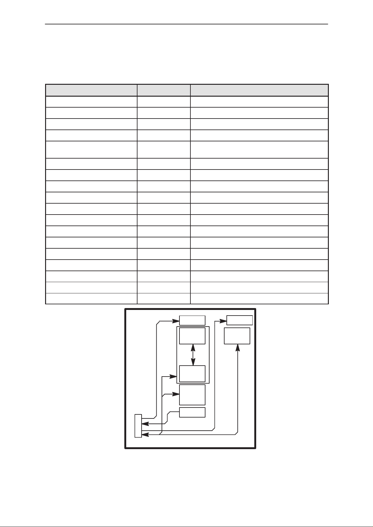
External Signals and Connections
Table 1. To Radio Module
Signal Name Pin / Conn. Notes
VL1 1 Logic supply voltage 3.15V
GND 2 Ground
V
BATT
BACKLIGHT 4 Backlights on/off
UIF(0:6) 5 – 11 Lines for keyboard read and LCD–controller
MIC_ENA 12 Microphone bias enable
COL(0:3) 13 – 16 Lines for keyboard write
CALL_LED 17 Call led enable
MICP 18 Microphone (positive node)
MICN 19 Microphone (negative node)
3, 30 Battery voltage
control
EARP 20 Earpiece (positive node)
EARN 21 Earpiece (negative node)
BUZZER 22 PWM signal buzzer control
XPWRON 23 Power key (active low)
VA2 24 Analog supply voltage 3.15V
NC 25,27,28
V
LCD
26 Supply voltage 4.0V for the LCD driver
AGND 29 Analog ground for the microphone
BUZZER
POWER
ON/OFF
UIF
Connector
EAR
DISPLAY
DISPLAY
DRIVER
KEY
BOARD
MIC
Issue 1 04/99
Figure 1. UIF Interconnection Diagram
Page 5–3
Page 4

NHP–4
Uif Module
Table 2. UIF Connector
Technical Documentation
Signal Name Pin / Conn. Notes
3VD 1 Logic supply voltage 3.15 V
GND 2, 29 Ground
VBATTERY 3, 30 Battery voltage
BACKLIGHT 4 Backlights on/off
UIF(0:6) 5 – 11 Lines for keyboard write and LCD–controller control
MIC_EN 12 Microphone bias enable (open drain, active low)
COL(0:3) 13 – 16 Lines for keyboard read
CALL_LED 17 Call led enable
MICP 18 Microphone (positive node)
MICN 19 Microphone (negative node)
EARN 20 Earpiece (negative node)
PAMS
EARP 21 Earpiece (positive node)
BUZZER 22 Buzzer control
ONKEYX 23 Power key (active low)
3VD 24 Analog supply voltage 3.15V
LCD_PWR 26 LCD supply voltage
SUNLIGHT 25 Connection to CALL LED for ambient light measurement
NC 27,28 NO CONNECT
1
.
.
.
.
30
Page 5–4
Figure 2. UIF Connections: Pin No. order
Issue 1 04/99
Page 5

PAMS
NHP–4
Technical Documentation
Table 3. To LCD Module
Pin Signal Name Notes
1 GND Ground
2,3 OSC1, OSC2 Oscillation terminals
4–8 V1–V5 LCD driving power source
9 V5OUT Negative voltage converter output
10–11 C1, C2 4.7 uF capacitor to generate negative
voltage for the input voltage VCI
12 VCI Power source for voltage converter
13 VCC Power source
14 RS Register selection
15 R/W Read/write
16 EN Enable for read/write signal
17–20 D(0–3) Data bus
Uif Module
21–24 D(4–7) Data bus
Functional Description
Circuit Description
Main components on the DU8 module
The module is connected with a 30 pin flex connector to the system board
and a 24 pin connector to the LCD module.
The module includes following main blocks:
– Keyboard
– Illumination
– Audio block
– LCD Module interface
Issue 1 04/99
Page 5–5
Page 6

NHP–4
Uif Module
Keyboard scanning and display driver control
COL(0–4) are used as column lines in keyboard. UIF(0–5) are used as
row lines. They are also multiplexed with display driver control signals.
When a key is pressed the ASIC gets an interrupt from a row and the
MCU starts scanning. One column at a time is written to low and rows are
used to read which key it was. The power off detection is multiplexed with
one row; when all keys on the row seems to be pressed the ASIC knows
that power key is pressed. The power key is also connected to PSL+ to
switch the power on.
Keyboard and display illumination
The keyboard illumination is achieved by using two transistors wired as
simple constant current sinks. Each transistor supplies eight leds. The
bases of the transistors are all wired together and supplied by emitter
follower V40. The led current is fixed by the values of R44 and R45 and
the ratio of R51 to R52.
PAMS
Technical Documentation
The display illumination operates in a similar way to the keyboard drivers,
two transistors are used to drive eight LED’s. The current in this case is
defined by the value of R46, R47 and the ratio of R51 to R52.
The Call LED is fed from a simple emitter follower.
Audio Circuitry
The earpiece is routed directly via series resistors to connector X4. The
earpiece is dynamic type.
The microphone is of the electric type and needs a voltage supply for
operation. When MIC_ENA is low bias voltage is connected to the
microphone via transistor V8. V2 is wired as a switch for VA2, controlled
by the microphone enable line [MICENA].
The buzzer is a dynamic one and is driven from a two transistor switch
which acts as a buffer for a CMOS output signal applied at BUZZER. The
ringing volume is controlled by pulse width modulation.The diode V37
prevents damage to the transistor when switched off, absorbing the stored
energy in the buzzer inductance and suppressing large positive going
spikes on the transistor collectors.
LCD Module Interface
The LCD module includes the LCD and the display driver. The driver TAB
is connected with heat seal connection to the LCD. Viewing direction is 6
o‘clock. It has internal clock oscillator and negative voltage generator.
The display module is connected to the UIF module with 24 pin soldered
connection.
Page 5–6
Issue 1 04/99
Page 7

PAMS
NHP–4
Technical Documentation
The display module contains an oscillator to generate a negative voltage
required for operation. The oscillator frequency is fixed on the UIF module
by the resistance from pins 2 to 3 of X1, with the values of R6 and R16
shown, the frequency is within 180 kHz to 370 kHz. The negative going
pulses appear at pin 9 of X1 where they are smoothed by C1 to give a
voltage which is nominally equal but opposite to VL1.
For correct operation of the display, DC voltages between –VL1 and VL1
need to be generated and fed back to the driver chip, at pins 4 to 8
inclusive (of X1). The exact voltages depend on the relative values of the
resistors R21, R37, R38, R39, R40 and R33.
Power Distribution Diagram
VA2
VL1
Uif Module
VL5VOLT
VBATT
GND
AGND
Call
LED
KEY/LC
D
Lights
Buzzer
Figure 3. Power Distribution
LCD
Keyboard
scan
Audio
Issue 1 04/99
Page 5–7
Page 8

NHP–4
Uif Module
Parts List – DU8D_06
p.n 0200521 EDMS issue 12.0
Item Code Description V alue Type
––––––––––––––––––––––––––––––––––––––––––––––––––––––––
R002 1430144 Chip jumper 0603
R003 1430144 Chip jumper 0603
R004 1430075 Chip resistor 33 k 5 % 0.063 W 0603
R005 1430087 Chip resistor 100 k 5 % 0.063 W 0603
R006 1430057 Chip resistor 8.2 k 5 % 0.063 W 0603
R009 1430087 Chip resistor 100 k 5 % 0.063 W 0603
R010 1430087 Chip resistor 100 k 5 % 0.063 W 0603
R011 1430087 Chip resistor 100 k 5 % 0.063 W 0603
R012 1430087 Chip resistor 100 k 5 % 0.063 W 0603
R013 1430087 Chip resistor 100 k 5 % 0.063 W 0603
R014 1430087 Chip resistor 100 k 5 % 0.063 W 0603
R015 1430087 Chip resistor 100 k 5 % 0.063 W 0603
R016 1430085 Chip resistor 82 k 5 % 0.063 W 0603
R017 1430087 Chip resistor 100 k 5 % 0.063 W 0603
R018 1430087 Chip resistor 100 k 5 % 0.063 W 0603
R021 1430075 Chip resistor 33 k 5 % 0.063 W 0603
R022 1430045 Chip resistor 2.7 k 5 % 0.063 W 0603
R023 1430045 Chip resistor 2.7 k 5 % 0.063 W 0603
R024 1430045 Chip resistor 2.7 k 5 % 0.063 W 0603
R025 1430045 Chip resistor 2.7 k 5 % 0.063 W 0603
R026 1430045 Chip resistor 2.7 k 5 % 0.063 W 0603
R028 1430075 Chip resistor 33 k 5 % 0.063 W 0603
R029 1430065 Chip resistor 10 k 5 % 0.063 W 0603
R030 1430045 Chip resistor 2.7 k 5 % 0.063 W 0603
R031 1430045 Chip resistor 2.7 k 5 % 0.063 W 0603
R033 1430069 Chip resistor 18 k 5 % 0.063 W 0603
R035 1430045 Chip resistor 2.7 k 5 % 0.063 W 0603
R037 1430063 Chip resistor 12 k 5 % 0.063 W 0603
R038 1430063 Chip resistor 12 k 5 % 0.063 W 0603
R039 1430063 Chip resistor 12 k 5 % 0.063 W 0603
R040 1430063 Chip resistor 12 k 5 % 0.063 W 0603
R044 1430165 Chip resistor 39 5 % 0.063 W 0603
R045 1430165 Chip resistor 39 5 % 0.063 W 0603
R046 1430165 Chip resistor 39 5 % 0.063 W 0603
R047 1430165 Chip resistor 39 5 % 0.063 W 0603
R048 1430045 Chip resistor 2.7 k 5 % 0.063 W 0603
R052 1430053 Chip resistor 5.6 k 5 % 0.063 W 0603
PAMS
Technical Documentation
Page 5–8
Issue 1 04/99
Page 9

PAMS
NHP–4
Technical Documentation
R054 1430087 Chip resistor 100 k 5 % 0.063 W 0603
C001 2604248 Tantalum cap. 4.7 u 20 % 16 V 6.0x3.2x2.5
C002 2604431 Tantalum cap. 10 u 20 % 16 V 6.0x3.2x2.5
C004 2604248 Tantalum cap. 4.7 u 20 % 16 V 6.0x3.2x2.5
C005 2307816 Ceramic cap. 47 n 20 % 25 V 0805
C006 2307816 Ceramic cap. 47 n 20 % 25 V 0805
C007 2307816 Ceramic cap. 47 n 20 % 25 V 0805
C008 2307816 Ceramic cap. 47 n 20 % 25 V 0805
C009 2307816 Ceramic cap. 47 n 20 % 25 V 0805
C010 2307816 Ceramic cap. 47 n 20 % 25 V 0805
C013 2604209 Tantalum cap. 1.0 u 20 % 16 V 3.2x1.6x1.6
C014 2320041 Ceramic cap. 18 p 5 % 50 V 0603
C015 2320041 Ceramic cap. 18 p 5 % 50 V 0603
C021 2320041 Ceramic cap. 18 p 5 % 50 V 0603
C023 2307816 Ceramic cap. 47 n 20 % 25 V 0805
C026 2307816 Ceramic cap. 47 n 20 % 25 V 0805
C027 2307816 Ceramic cap. 47 n 20 % 25 V 0805
C030 2320041 Ceramic cap. 18 p 5 % 50 V 0603
C031 2320041 Ceramic cap. 18 p 5 % 50 V 0603
C040 2320107 Ceramic cap. 10 n 5 % 50 V 0603
B001 5140125 Buzzer 90db 2700hz 5.0v d9.0x5.5
B002 5140446 Cond. microphone 62+–2DB 2.2K PCPCB
B003 5140576 Speaker 95.5+–2DB 32R D20X2
V002 4200829 Transistor BC859C pnp 30 V 0.1 A SOT23
V003 4200811 Transistor BC849C npn 30 V 0.1 A SOT23
V004 4200836 Transistor BCX19 npn 50 V 0.5 A SOT23
V005 4200811 Transistor BC849C npn 30 V 0.1 A SOT23
V008 4200811 Transistor BC849C npn 30 V 0.1 A SOT23
V010 4864384 Led Red 0603
V011 4864388 Led Green 0603
V012 4864388 Led Green 0603
V013 4864388 Led Green 0603
V014 4864388 Led Green 0603
V015 4864388 Led Green 0603
V016 4864388 Led Green 0603
V017 4864388 Led Green 0603
V018 4864388 Led Green 0603
V019 4864388 Led Green 0603
V020 4864388 Led Green 0603
V021 4864388 Led Green 0603
V022 4864388 Led Green 0603
V023 4864388 Led Green 0603
V024 4864388 Led Green 0603
Uif Module
Issue 1 04/99
Page 5–9
Page 10

NHP–4
Uif Module
V025 4864388 Led Green 0603
V026 4864388 Led Green 0603
V027 4864388 Led Green 0603
V028 4864388 Led Green 0603
V029 4864388 Led Green 0603
V030 4864388 Led Green 0603
V031 4864388 Led Green 0603
V032 4864388 Led Green 0603
V033 4864388 Led Green 0603
V034 4864388 Led Green 0603
V036 4111824 DiodeBAS16 75 V 250 mA 6 ns SOT23
V037 4111824 DiodeBAS16 75 V 250 mA 6 ns SOT23
V040 4200811 Transistor BC849C npn 30 V 0.1 A SOT23
V041 4200836 Transistor BCX19 npn 50 V 0.5 A SOT23
V042 4200836 Transistor BCX19 npn 50 V 0.5 A SOT23
V043 4200836 Transistor BCX19 npn 50 V 0.5 A SOT23
V044 4200836 Transistor BCX19 npn 50 V 0.5 A SOT23
PAMS
Technical Documentation
4850038 IC, lcd 42dotm 3x7sgm 57ind DSL–12 EU
9460074 Light guide 4c23228 nhj– 1DA
9460075 Microphone rubber 4d22908 nhj–1DNHJ–1DA
9480061 Reflector 3c22893 nhj–1DA
9480078 Buzzer gasket 4D23092 NHK–1XA
9480103 Speaker pad2 4D23517 NHK–1XA
9480134 Speaker gasket 4D24016 NHK–1XA
9795021 Main keydome 3C26395 NHC–4NX
9795022 Side keydome 4C26397 NHC–4NX
9855017 PCB DU8D 50.0X141.0
9855017 PC board DU8D 50.0x141.0
Page 5–10
Issue 1 04/99
 Loading...