

Page 1

UIF MODULES DU4, DL4 & GU3
NHC–1/4
0697JR
Technical Documentation
Copyright Nokia Mobile Phones
Contents
UIF modules DU4, DL4 & GU3 9–2. . . . . . . . . . . . . . . . . . . . . . . . . . .
General 9–2. . . . . . . . . . . . . . . . . . . . . . . . . . . . . . . . . . . . . . . . . . . . .
Hierarchy of design 9–2. . . . . . . . . . . . . . . . . . . . . . . . . . . . . . . . .
Mechanical differences between modules DU4 and DL4 9–3.
Technical specifications 9–4. . . . . . . . . . . . . . . . . . . . . . . . . . . . . . .
External signals and connectors 9–4. . . . . . . . . . . . . . . . . . . . . .
UIF module main connector X4 9–4. . . . . . . . . . . . . . . . . . . .
Display module connector X1 9–5. . . . . . . . . . . . . . . . . . . . . .
Supply voltages and power consumption 9–6. . . . . . . . . . . .
Control signals 9–6. . . . . . . . . . . . . . . . . . . . . . . . . . . . . . . . . .
Audio specifications 9–6. . . . . . . . . . . . . . . . . . . . . . . . . . . . . .
Functional description 9–7. . . . . . . . . . . . . . . . . . . . . . . . . . . . . . . . .
Circuit description 9–7. . . . . . . . . . . . . . . . . . . . . . . . . . . . . . . . . .
LED drivers 9–7. . . . . . . . . . . . . . . . . . . . . . . . . . . . . . . . . . . . .
Call indicator 9–7. . . . . . . . . . . . . . . . . . . . . . . . . . . . . . . . . . . .
Buzzer driver 9–7. . . . . . . . . . . . . . . . . . . . . . . . . . . . . . . . . . . .
Audio circuitry 9–7. . . . . . . . . . . . . . . . . . . . . . . . . . . . . . . . . . .
RF suppression 9–8. . . . . . . . . . . . . . . . . . . . . . . . . . . . . . . . . .
Display driver 9–8. . . . . . . . . . . . . . . . . . . . . . . . . . . . . . . . . . .
Power distribution diagram 9–9. . . . . . . . . . . . . . . . . . . . . . . .
Circuit Diagram of DU4 9–10. . . . . . . . . . . . . . . . . . . . . . . . . . . . . . . .
Circuit Diagram of DL4 9–11. . . . . . . . . . . . . . . . . . . . . . . . . . . . . . . .
Circuit Diagram of GU3 9–12. . . . . . . . . . . . . . . . . . . . . . . . . . . . . . . .
Layout Diagram of DU4 (version 07) 9–13. . . . . . . . . . . . . . . . . . . .
Layout Diagram of DL4 (version 06) 9–14. . . . . . . . . . . . . . . . . . . . .
Layout Diagram of GU3 (version 03) 9–15. . . . . . . . . . . . . . . . . . . .
Parts list of DU4 EDMS issue: 5.4 Code: 0200175 layout 07 9–16
Parts list of DL4 EDMS issue: 4.2 Code: 0200176 layout 06 9–19
Parts list of GU3 EDMS issue: 3.1 Code: 0200629 layout 03 9–22
9–1
Page 2
UIF MODULES DU4, DL4 & GU3
NHC–1/4
0697JR
Technical Documentation
UIF modules DU4, DL4 & GU3
General
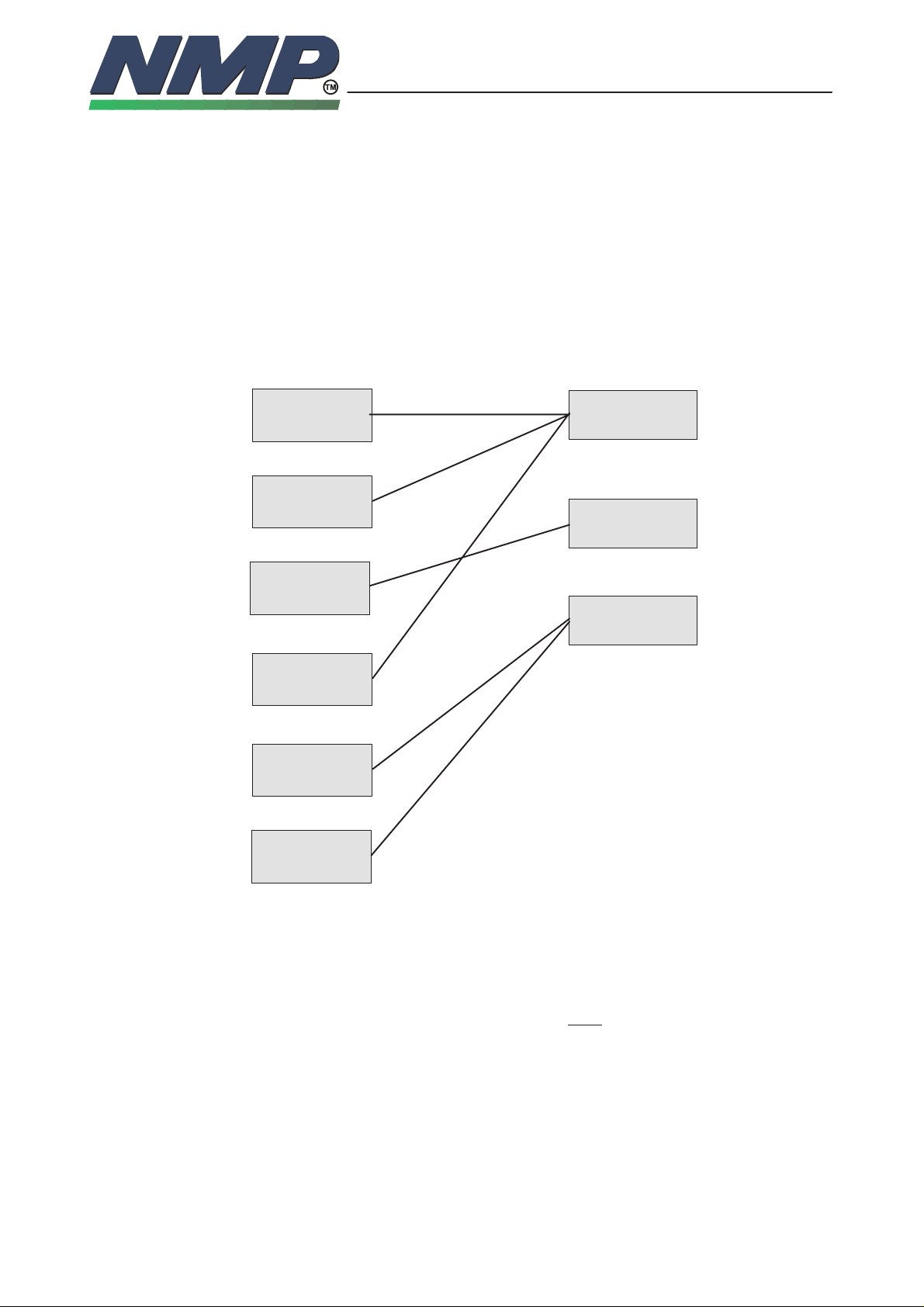
Three modules are described in this document. They are similar – the only dif-
ference is the keyboard layout and an amount of LEDs. The three modules are
used in the different US TDMA (NHC–1 and NHC–4) phones as shown in fol-
lowing picture:
PHONES
US TDMA
NHC–4NX,4HX
0500397,–510
US TDMA
NHC–4NE,4NV
0500687,–88
9–2
Copyright Nokia Mobile Phones
USER INTERFACE MODULES
DU4
0200175
GU3
0200629
US TDMA
NHC–4NB,4HB
0500591,–92
US TDMA
NHC–1XN
05001 16
US TDMA
NHC–1XA
05001 18
US TDMA
NHC–1XB
0500121
Hierarchy of design
There is a high degree of commonality between these designs.
Technically there are two schematics.
The difference between the two PCB layouts is only
LEDs (and one less LED on the Style 1 version). The DU4 layout has 20 main
keys, 2 volume keys at the side of the flex and a power key in the upper right
corner of the flex. DL4 flexis have 20 main keys in a slightly different layout and
the volume/power keys combined on one assembly.
DL4
0200176
the position of the keys &
The GU3 has one LED less than DU4. Volume and power keys are as in DU4.
Page 3
UIF MODULES DU4, DL4 & GU3
NHC–1/4
0697JR
Technical Documentation
Copyright Nokia Mobile Phones
Mechanical differences between modules DU4 and DL4
9–3
X4
1
30
X4
1
30
DU4 DL4
Page 4

UIF MODULES DU4, DL4 & GU3
NHC–1/4
0697JR
Technical Documentation
Technical specifications
External signals and connectors
The UIF module has two connector, display module connector X1 and main
connector X4.
UIF module main connector X4
Pin: Name: Description:
1 VL1 Supply voltage
2 GND Ground
3, 30 VBATT Battery voltage
4 KEYLIGHT Backlighting control for keymat only
5–10 UIF0–UIF5 LCD driving and keyboard ROW reading
9–4
Copyright Nokia Mobile Phones
11 UIF6 LCD driving only
12 LCDLIGHT Backlighting control for LCD only
13–16 COL0–COL3 Column scan for key matrix
17, 20 GND Microphone ground
18 MICP Positive microphone terminal
19 MICN Negative microphone terminal
21 EARN Negative earpiece terminal
22 EARP Positive earpiece terminal
23 VA2 Supply voltage
24 XPWRON Power control for system
25 NC No connection
26 MIC_EN To enable all audio circuitry
27 NC No connection
28 CALL_LED Call indicator LED
29 BUZZER Buzzer control input
Page 5
UIF MODULES DU4, DL4 & GU3
NHC–1/4
Display module connector X1
Heatseal
X1
0
25
0697JR
Technical Documentation
LCD
IC
TAB
9–5
Copyright Nokia Mobile Phones
Pin: Name: Description:
0, 25 NC End connections to add mechanical
strenght to solder joint
1V
SS
Power source, 0 V
2, 3 OSC1, OSC2 Oscillator terminals
4–8 V1–V8 LCD driving power source;
DD
–
1.0
/
6.7 VLCD
2.0
/
6.7 VLCD
4.7
/
6.7 VLCD
5.7
/
6.7 VLCD
6.7
/
6.7 VLCD
9V
5out
• V1 = V
• V2 = VDD –
• V3 = VDD –
• V4 = VDD –
• V5 = VDD –
Voltage converter output
10, 11 C1, C2 Capacitor connecting terminals for voltage
12 V
13 V
ci
DD
doupler for the input voltage V
Power source for voltage converter
Power source, +5 V
(C1; +, C2; –)
ci
14 RS Register selection signal input
15 R/W Read ”1”/write ”0” signal
16 E Read/write activation signal
17–20 DB
21–24 DB
–DB
0
–DB
4
3
7
3 state data bus (lower)
3 state data bus (upper), DB7 is also used
for busy flag reading
Page 6

UIF MODULES DU4, DL4 & GU3
NHC–1/4
0697JR
Technical Documentation
Supply voltages and power consumption
Symbol: Description: Values:
VL1 Logic voltage
• min/typ/max voltage:
• typical current:
VA2 Analog voltage
• min/typ/max voltage:
• typical current:
VBATT Supply voltage
• min/typ/max voltage:
• typical current:
Control signals
Symbol: Description: Values:
9–6
Copyright Nokia Mobile Phones
4.5...4.65...4.8 V
1.4 mA
4.5...4.65...4.8 V
1 mA
5.3...6.5...8.8 V
250 mA
MIC_EN Microphone enable
KEYLIGHT Backlighting control
LCDLIGHT LCD backlighting control
CALL_LED Call indicator LED control
Audio specifications
Symbol: Description: Values:
MICN–MICP Microphone sensitivity
• enabled typ/max voltage:
• disabled min/typ/max volt:
• lights on min/max voltage:
• lights off min/max voltage:
• lights on min/max voltage:
• lights off min/max voltage:
• LED on min/max voltage:
• LED off min/max voltage:
• 97 dB
input to microphone
SPL
at 25 mm:
0...3 V
VA1–0.4...VA1...VA1+3 V
VA1–1.0...VA1 V
0...2 V
VA1–1.0...VA1 V
0...2 V
VA1–1.0...VA1 V
0...0.4 V
5 mV
RMS
EARP–EARN Earphone sensitivity
• with 60 mV
across EARP
RMS
EARN at 1 kHz min/typ/max:
MICN Frequency responce
• measured from 300 Hz to 3 kHz
with input of 97 dB
at 25 mm:
SPL
91...94...97 dB
–4.0...+4.0 dB
SPL
Page 7

UIF MODULES DU4, DL4 & GU3
NHC–1/4
Functional description
The following sections of circuitry are included on the module:
– Microphone circuit (differential)
– Speaker circuit
– LCD display module
– LCD voltage divider & temperature compensation circuit
– Keyboard & display lighting circuits
– Keyboard switch matrix
Circuit description
LED drivers
The keyboard illumination is achieved by using four transistors wired as simple
constant current sinks. Each transistor supplies four leds. The bases of the six
transistor are all wired together and supplied by emitter follower V40. The led
current is fixed by the values of (R44 to R47 inclusive) and the ratio of R59 to
R57.
Note that on DL4 flexi, a 18
0697JR
Technical Documentation
th
led (V38) is driven from an additional transistor.
9–7
Copyright Nokia Mobile Phones
The display illumination operates in a similar way to the keyboard drivers, but
only two transistors are used to drive eight leds. The current in this case is defined by the value of R42 and R43 and the ratio of R60 to R61.
Call indicator
The Call LED is fed from a simple emitter follower.
Buzzer driver
The buzzer driver circuit consists of four transistor switches wired in parallel.
The buzzer takes relatively large peak currents and four switches are used to
minimise temperature rise in the driver during ringing. All four are driven from a
single PNP– transistor switch which acts as a buffer for a CMOS output signal
applied at BUZZER.
The diode V37 prevents damage to the transistors when they switch off, absorbing the stored energy in the buzzer inductance and suppressing large positive going spikes on the transistor collectors.
Audio circuitry
The audio circuitry comprises a switched analogue supply rail (Vx). The switching is used to avoid wasting current when the phone is in standby.
The earpiece is routed directly to connector X4.
Page 8

UIF MODULES DU4, DL4 & GU3
NHC–1/4
VA2 is an analogue rail supplied by the PSL+ chip on the system board. It is
present whenever the battery is connected and is 4.65 V in magnitude. V2 is
wired as a switch for VA2, controlled by the microphone enable line [MIC_EN],
in this case a CMOS output from the processor.
V9 and its associated components act as a filter to reduce any noise on the
VA2 line, R29 and C13/C14 acting as a lowpass filter with a –3 dB point of
about 179 Hz. The filter feeds a smooth dc voltage to the base of emitter follower V9. Its emitter provides the clean analogue supply for the transistor amplifiers.
The microphone is connected to two equal value connectors, one of which connects the positive mic terminal to Vx, the other connects the negative terminal
to GND. The signal is capacitively coupled to the MICN and MICP terminals of
X4 via C26 and C27.
RF suppression
Small value capacitors are fitted at critical points in the circuit to try to avoid
problems with RF interference. One each is placed directly across each microphone (C15). V9 has a cap to ground from each of its three terminals (C20,
C21, C22) and V2 a cap from its base drive pin to ground (C19).
0697JR
Technical Documentation
9–8
Copyright Nokia Mobile Phones
Display driver
Only the dc bias circuitry will be described here, the method of control of the
display being outlined elsewhere. Also refer to Display Module Spec if necessary. The module contains an oscillator to generate a negative rail required for
operation. The oscillator frequency is fixed by the resistance from pins 2 to 3 of
X1, with the values of R6 and R16 shown, the frequency should be within
180 kHz to 370 kHz. The negative going pulses appear at pin 9 of X1 where
they are smoothed by C1 to give a voltage which is nominally equal but opposite to VL1.
For correct operation of the display, dc voltages between –VL1 and VL1 need
to be generated and fed back to the driver chip, at pins 4 to 8 inclusive (of X1).
The exact voltages depend on the relative values of the resistors R21, R37,
R38, R39, R40 and R27, R33. R1 is a thermistor which provides temperature
compensation for the display. To maintain consistent contrast over temperature,
these derived voltages need to be altered slightly, R1 provides this function.
Page 9

UIF MODULES DU4, DL4 & GU3
NHC–1/4
Power distribution diagram
VA2
VL1
Vbatt
Call
LED
LCD
Lights
GND
0697JR
Technical Documentation
Key
Lights
Buzzer LCD
9–9
Copyright Nokia Mobile Phones
Keyboard
scan
Audio
Page 10

UIF MODULES DU4, DL4 & GU3
NHC–1/4
Circuit Diagram of DU4
0697JR
Technical Documentation
9–10
Copyright Nokia Mobile Phones
Page 11

UIF MODULES DU4, DL4 & GU3
NHC–1/4
Circuit Diagram of DL4
0697JR
Technical Documentation
9–11
Copyright Nokia Mobile Phones
Page 12

UIF MODULES DU4, DL4 & GU3
NHC–1/4
0697JR
Technical Documentation
Circuit Diagram of GU3
9–12
Copyright Nokia Mobile Phones
Page 13

UIF MODULES DU4, DL4 & GU3
NHC–1/4
0697JR
Technical Documentation
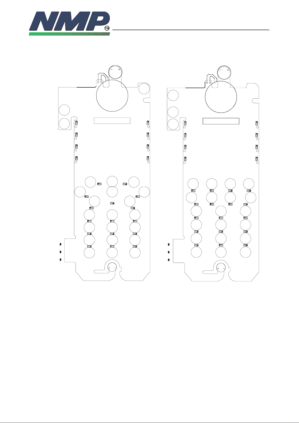
Layout Diagram of DU4 (version 07)
9–13
Copyright Nokia Mobile Phones
Page 14

UIF MODULES DU4, DL4 & GU3
NHC–1/4
0697JR
Technical Documentation
Layout Diagram of DL4 (version 06)
9–14
Copyright Nokia Mobile Phones
Page 15

UIF MODULES DU4, DL4 & GU3
NHC–1/4
0697JR
Technical Documentation
Layout Diagram of GU3 (version 03)
9–15
Copyright Nokia Mobile Phones
Page 16

UIF MODULES DU4, DL4 & GU3
NHC–1/4
0697JR
Technical Documentation
Copyright Nokia Mobile Phones
Parts list of DU4 EDMS issue: 5.4 Code: 0200175 for layout version 07
ITEM CODE DESCRIPTION VALUE TYPE
R006 1430057 Chip resistor 8.2 k 5 % 0.063 W 0603
R009 1430087 Chip resistor 100 k 5 % 0.063 W 0603
R010 1430087 Chip resistor 100 k 5 % 0.063 W 0603
R011 1430087 Chip resistor 100 k 5 % 0.063 W 0603
R012 1430087 Chip resistor 100 k 5 % 0.063 W 0603
R013 1430087 Chip resistor 100 k 5 % 0.063 W 0603
R014 1430087 Chip resistor 100 k 5 % 0.063 W 0603
R015 1430087 Chip resistor 100 k 5 % 0.063 W 0603
R016 1430085 Chip resistor 82 k 5 % 0.063 W 0603
R017 1430087 Chip resistor 100 k 5 % 0.063 W 0603
R021 1430075 Chip resistor 33 k 5 % 0.063 W 0603
R022 1430065 Chip resistor 10 k 5 % 0.063 W 0603
R023 1430065 Chip resistor 10 k 5 % 0.063 W 0603
R024 1430065 Chip resistor 10 k 5 % 0.063 W 0603
R025 1430065 Chip resistor 10 k 5 % 0.063 W 0603
R026 1430065 Chip resistor 10 k 5 % 0.063 W 0603
R029 1430065 Chip resistor 10 k 5 % 0.063 W 0603
R030 1430051 Chip resistor 4.7 k 5 % 0.063 W 0603
R031 1430051 Chip resistor 4.7 k 5 % 0.063 W 0603
R032 1430013 Chip resistor 330 5 % 0.063 W 0603
R033 1430075 Chip resistor 33 k 5 % 0.063 W 0603
R035 1430035 Chip resistor 1.0 k 5 % 0.063 W 0603
R037 1430063 Chip resistor 12 k 5 % 0.063 W 0603
R038 1430063 Chip resistor 12 k 5 % 0.063 W 0603
R039 1430063 Chip resistor 12 k 5 % 0.063 W 0603
R040 1430063 Chip resistor 12 k 5 % 0.063 W 0603
R042 1430171 Chip resistor 68 5 % 0.063 W 0603
R043 1430171 Chip resistor 68 5 % 0.063 W 0603
R044 1430171 Chip resistor 68 5 % 0.063 W 0603
R045 1430171 Chip resistor 68 5 % 0.063 W 0603
R046 1430171 Chip resistor 68 5 % 0.063 W 0603
R047 1430171 Chip resistor 68 5 % 0.063 W 0603
R048 1412335 Chip resistor 1.0 k 5 % 0.1 W 0805
R049 1430159 Chip resistor 22 5 % 0.063 W 0603
R050 1430159 Chip resistor 22 5 % 0.063 W 0603
R051 1430159 Chip resistor 22 5 % 0.063 W 0603
R052 1430159 Chip resistor 22 5 % 0.063 W 0603
R053 1430013 Chip resistor 330 5 % 0.063 W 0603
R056 1430087 Chip resistor 100 k 5 % 0.063 W 0603
R057 1430051 Chip resistor 4.7 k 5 % 0.063 W 0603
R058 1430087 Chip resistor 100 k 5 % 0.063 W 0603
R059 1430051 Chip resistor 4.7 k 5 % 0.063 W 0603
R060 1430051 Chip resistor 4.7 k 5 % 0.063 W 0603
9–16
Page 17

UIF MODULES DU4, DL4 & GU3
NHC–1/4
0697JR
Technical Documentation
Copyright Nokia Mobile Phones
R061 1430051 Chip resistor 4.7 k 5 % 0.063 W 0603
R062 1430087 Chip resistor 100 k 5 % 0.063 W 0603
C001 2604248 Tantalum cap. 4.7 u 20 % 16 V 6.0x3.2x2.5
C002 2604431 Tantalum cap. 10 u 20 % 16 V 6.0x3.2x2.5
C004 2604248 Tantalum cap. 4.7 u 20 % 16 V 6.0x3.2x2.5
C006 2307816 Ceramic cap. 47 n 20 % 25 V 0805
C013 2307816 Ceramic cap. 47 n 20 % 25 V 0805
C014 2307816 Ceramic cap. 47 n 20 % 25 V 0805
C015 2320059 Ceramic cap. 100 p 5 % 50 V 0603
C017 2320107 Ceramic cap. 10 n 5 % 50 V 0603
C019 2320041 Ceramic cap. 18 p 5 % 50 V 0603
C020 2320041 Ceramic cap. 18 p 5 % 50 V 0603
C021 2320041 Ceramic cap. 18 p 5 % 50 V 0603
C022 2320041 Ceramic cap. 18 p 5 % 50 V 0603
C026 2307816 Ceramic cap. 47 n 20 % 25 V 0805
C027 2307816 Ceramic cap. 47 n 20 % 25 V 0805
C028 2320041 Ceramic cap. 18 p 5 % 50 V 0603
C029 2320041 Ceramic cap. 18 p 5 % 50 V 0603
B001 5140014 Buzzer transducer 90db 25r pc PCB
B002 5140063 Cond. microphone 44 +– 2DB 2.2K PCPCB
B003 5140576 Dynamic receiver 32r 20x2 20x2
V002 4219894 Transistor x 2 IMB7 pnp –5 V –0.1 A IMD
V003 4219912 Transistor x 2 IMX1 npn 40 V 0.1 A IMD
V004 4219912 Transistor x 2 IMX1 npn 40 V 0.1 A IMD
V005 4219912 Transistor x 2 IMX1 npn 40 V 0.1 A IMD
V006 4219912 Transistor x 2 IMX1 npn 40 V 0.1 A IMD
V007 4219912 Transistor x 2 IMX1 npn 40 V 0.1 A IMD
V009 4219912 Transistor x 2 IMX1 npn 40 V 0.1 A IMD
V010 4864384 Led Red 0603
V011 4864388 Led Green 0603
V012 4864388 Led Green 0603
V013 4864388 Led Green 0603
V014 4864388 Led Green 0603
V015 4864388 Led Green 0603
V016 4864388 Led Green 0603
V017 4864388 Led Green 0603
V018 4864388 Led Green 0603
V019 4864388 Led Green 0603
V020 4864388 Led Green 0603
V021 4864388 Led Green 0603
V022 4864388 Led Green 0603
V023 4864388 Led Green 0603
V024 4864388 Led Green 0603
V025 4864388 Led Green 0603
V026 4864388 Led Green 0603
V027 4864388 Led Green 0603
V028 4864388 Led Green 0603
V029 4864388 Led Green 0603
9–17
Page 18

UIF MODULES DU4, DL4 & GU3
NHC–1/4
0697JR
Technical Documentation
Copyright Nokia Mobile Phones
9–18
V030 4864388 Led Green 0603
V031 4864388 Led Green 0603
V032 4864388 Led Green 0603
V033 4864388 Led Green 0603
V034 4864388 Led Green 0603
V035 4219912 Transistor x 2 IMX1 npn 40 V 0.1 A IMD
V036 4111824 Diode BAS16 75 V 250 mA 6 ns SOT23
V037 4111824 Diode BAS16 75 V 250 mA 6 ns SOT23
V040 4219912 Transistor x 2 IMX1 npn 40 V 0.1 A IMD
4850038 IC, lcd 42dotm 3x7sgm 57ind DSL–12 EU
9460074 Light guide 4c23228 nhj–1DA
9460075 Microphone rubber 4d22908 nhj–1D NHJ–1DA
9480061 Reflector 3c22893 nhj–1DA
9480078 Buzzer gasket 4D23092 NHK–1XA
9480134 Speaker gasket 4D24016 NHK–1XA
9480324 Buzzer pad dmd02461
9480326 Speaker pad dmd02577 nhc–4xx nhc–4xx
9795021 Main keydome 3C26395 NHC–4NX
9795022 Side keydome 4C26397 NHC–4NX
9855012 PCB DU4 141.5X60.5 D NHC–1XN
9855012 PC board DU4 141.5x60.5d nhc–1x NHC–1XN
Page 19

UIF MODULES DU4, DL4 & GU3
NHC–1/4
0697JR
Technical Documentation
Copyright Nokia Mobile Phones
Parts list of DL4 EDMS issue: 4.2 Code: 0200176 for layout version 06
ITEM CODE DESCRIPTION VALUE TYPE
R006 1430057 Chip resistor 8.2 k 5 % 0.063 W 0603
R009 1430087 Chip resistor 100 k 5 % 0.063 W 0603
R010 1430087 Chip resistor 100 k 5 % 0.063 W 0603
R011 1430087 Chip resistor 100 k 5 % 0.063 W 0603
R012 1430087 Chip resistor 100 k 5 % 0.063 W 0603
R013 1430087 Chip resistor 100 k 5 % 0.063 W 0603
R014 1430087 Chip resistor 100 k 5 % 0.063 W 0603
R015 1430087 Chip resistor 100 k 5 % 0.063 W 0603
R016 1430085 Chip resistor 82 k 5 % 0.063 W 0603
R017 1430087 Chip resistor 100 k 5 % 0.063 W 0603
R021 1430075 Chip resistor 33 k 5 % 0.063 W 0603
R022 1430065 Chip resistor 10 k 5 % 0.063 W 0603
R023 1430065 Chip resistor 10 k 5 % 0.063 W 0603
R024 1430065 Chip resistor 10 k 5 % 0.063 W 0603
R025 1430065 Chip resistor 10 k 5 % 0.063 W 0603
R026 1430065 Chip resistor 10 k 5 % 0.063 W 0603
R029 1430065 Chip resistor 10 k 5 % 0.063 W 0603
R030 1430051 Chip resistor 4.7 k 5 % 0.063 W 0603
R031 1430051 Chip resistor 4.7 k 5 % 0.063 W 0603
R032 1430013 Chip resistor 330 5 % 0.063 W 0603
R033 1430075 Chip resistor 33 k 5 % 0.063 W 0603
R035 1430035 Chip resistor 1.0 k 5 % 0.063 W 0603
R037 1430063 Chip resistor 12 k 5 % 0.063 W 0603
R038 1430063 Chip resistor 12 k 5 % 0.063 W 0603
R039 1430063 Chip resistor 12 k 5 % 0.063 W 0603
R040 1430063 Chip resistor 12 k 5 % 0.063 W 0603
R042 1430171 Chip resistor 68 5 % 0.063 W 0603
R043 1430171 Chip resistor 68 5 % 0.063 W 0603
R044 1430171 Chip resistor 68 5 % 0.063 W 0603
R045 1430171 Chip resistor 68 5 % 0.063 W 0603
R046 1430171 Chip resistor 68 5 % 0.063 W 0603
R047 1430171 Chip resistor 68 5 % 0.063 W 0603
R048 1412335 Chip resistor 1.0 k 5 % 0.1 W 0805
R049 1430159 Chip resistor 22 5 % 0.063 W 0603
R050 1430159 Chip resistor 22 5 % 0.063 W 0603
R051 1430159 Chip resistor 22 5 % 0.063 W 0603
R052 1430159 Chip resistor 22 5 % 0.063 W 0603
R053 1430013 Chip resistor 330 5 % 0.063 W 0603
R054 1430005 Chip resistor 150 5 % 0.063 W 0603
R056 1430087 Chip resistor 100 k 5 % 0.063 W 0603
R057 1430051 Chip resistor 4.7 k 5 % 0.063 W 0603
R058 1430087 Chip resistor 100 k 5 % 0.063 W 0603
R059 1430051 Chip resistor 4.7 k 5 % 0.063 W 0603
9–19
Page 20

UIF MODULES DU4, DL4 & GU3
NHC–1/4
0697JR
Technical Documentation
Copyright Nokia Mobile Phones
R060 1430051 Chip resistor 4.7 k 5 % 0.063 W 0603
R061 1430051 Chip resistor 4.7 k 5 % 0.063 W 0603
R062 1430087 Chip resistor 100 k 5 % 0.063 W 0603
C001 2604248 Tantalum cap. 4.7 u 20 % 16 V 6.0x3.2x2.5
C002 2604431 Tantalum cap. 10 u 20 % 16 V 6.0x3.2x2.5
C004 2604248 Tantalum cap. 4.7 u 20 % 16 V 6.0x3.2x2.5
C006 2307816 Ceramic cap. 47 n 20 % 25 V 0805
C013 2307816 Ceramic cap. 47 n 20 % 25 V 0805
C014 2307816 Ceramic cap. 47 n 20 % 25 V 0805
C015 2320059 Ceramic cap. 100 p 5 % 50 V 0603
C017 2320107 Ceramic cap. 10 n 5 % 50 V 0603
C019 2320041 Ceramic cap. 18 p 5 % 50 V 0603
C020 2320041 Ceramic cap. 18 p 5 % 50 V 0603
C021 2320041 Ceramic cap. 18 p 5 % 50 V 0603
C022 2320041 Ceramic cap. 18 p 5 % 50 V 0603
C026 2307816 Ceramic cap. 47 n 20 % 25 V 0805
C027 2307816 Ceramic cap. 47 n 20 % 25 V 0805
C028 2320041 Ceramic cap. 18 p 5 % 50 V 0603
C029 2320041 Ceramic cap. 18 p 5 % 50 V 0603
B001 5140014 Buzzer transducer 90db 25r pc PCB
B002 5140063 Cond. microphone 44 +– 2DB 2.2K PCPCB
B003 5140576 Dynamic receiver 32r 20x2 20x2
V002 4219894 Transistor x 2 IMB7 pnp –5 V –0.1 A IMD
V003 4219912 Transistor x 2 IMX1 npn 40 V 0.1 A IMD
V004 4219912 Transistor x 2 IMX1 npn 40 V 0.1 A IMD
V005 4219912 Transistor x 2 IMX1 npn 40 V 0.1 A IMD
V006 4219912 Transistor x 2 IMX1 npn 40 V 0.1 A IMD
V007 4219912 Transistor x 2 IMX1 npn 40 V 0.1 A IMD
V009 4219912 Transistor x 2 IMX1 npn 40 V 0.1 A IMD
V010 4864384 Led Red 0603
V011 4864388 Led Green 0603
V012 4864388 Led Green 0603
V013 4864388 Led Green 0603
V014 4864388 Led Green 0603
V015 4864388 Led Green 0603
V016 4864388 Led Green 0603
V017 4864388 Led Green 0603
V018 4864388 Led Green 0603
V019 4864388 Led Green 0603
V020 4864388 Led Green 0603
V021 4864388 Led Green 0603
V022 4864388 Led Green 0603
V023 4864388 Led Green 0603
V024 4864388 Led Green 0603
V025 4864388 Led Green 0603
V026 4864388 Led Green 0603
V027 4864388 Led Green 0603
V028 4864388 Led Green 0603
9–20
Page 21

UIF MODULES DU4, DL4 & GU3
NHC–1/4
0697JR
Technical Documentation
Copyright Nokia Mobile Phones
9–21
V029 4864388 Led Green 0603
V030 4864388 Led Green 0603
V031 4864388 Led Green 0603
V032 4864388 Led Green 0603
V033 4864388 Led Green 0603
V034 4864388 Led Green 0603
V035 4219912 Transistor x 2 IMX1 npn 40 V 0.1 A IMD
V036 4111824 Diode BAS16 75 V 250 mA 6 ns SOT23
V037 4111824 Diode BAS16 75 V 250 mA 6 ns SOT23
V038 4864388 Led Green 0603
V040 4219912 Transistor x 2 IMX1 npn 40 V 0.1 A IMD
4850038 IC, lcd 42dotm 3x7sgm 57ind DSL–12 EU
9460074 Light guide 4c23228 nhj–1DA
9460075 Microphone rubber 4d22908 nhj– 1D NHJ–1DA
9480061 Reflector 3c22893 nhj–1DA
9480078 Buzzer gasket 4D23092 NHK–1XA
9480324 Buzzer pad dmd02461
9480326 Speaker pad dmd02577 nhc–4xx nhc–4xx
9795003 Keydome film 4c22987 nhj–1DA
9855013 PCB DL4 141.5X60.5 D NHC–1XA
9855013 PC board DL4 141.5x60.5d nhc–1x NHC–1XA
Page 22

UIF MODULES DU4, DL4 & GU3
NHC–1/4
0697JR
Technical Documentation
Copyright Nokia Mobile Phones
Parts list of GU3 EDMS issue: 3.1 Code: 0200629 for layout version 03
ITEM CODE DESCRIPTION VALUE TYPE
R006 1430057 Chip resistor 8.2 k 5 % 0.063 W 0603
R009 1430087 Chip resistor 100 k 5 % 0.063 W 0603
R010 1430087 Chip resistor 100 k 5 % 0.063 W 0603
R011 1430087 Chip resistor 100 k 5 % 0.063 W 0603
R012 1430087 Chip resistor 100 k 5 % 0.063 W 0603
R013 1430087 Chip resistor 100 k 5 % 0.063 W 0603
R014 1430087 Chip resistor 100 k 5 % 0.063 W 0603
R015 1430087 Chip resistor 100 k 5 % 0.063 W 0603
R016 1430085 Chip resistor 82 k 5 % 0.063 W 0603
R017 1430087 Chip resistor 100 k 5 % 0.063 W 0603
R021 1430075 Chip resistor 33 k 5 % 0.063 W 0603
R022 1430065 Chip resistor 10 k 5 % 0.063 W 0603
R023 1430065 Chip resistor 10 k 5 % 0.063 W 0603
R024 1430065 Chip resistor 10 k 5 % 0.063 W 0603
R025 1430065 Chip resistor 10 k 5 % 0.063 W 0603
R026 1430065 Chip resistor 10 k 5 % 0.063 W 0603
R029 1430065 Chip resistor 10 k 5 % 0.063 W 0603
R030 1430051 Chip resistor 4.7 k 5 % 0.063 W 0603
R031 1430051 Chip resistor 4.7 k 5 % 0.063 W 0603
R032 1430013 Chip resistor 330 5 % 0.063 W 0603
R033 1430075 Chip resistor 33 k 5 % 0.063 W 0603
R035 1430035 Chip resistor 1.0 k 5 % 0.063 W 0603
R037 1430063 Chip resistor 12 k 5 % 0.063 W 0603
R038 1430063 Chip resistor 12 k 5 % 0.063 W 0603
R039 1430063 Chip resistor 12 k 5 % 0.063 W 0603
R040 1430063 Chip resistor 12 k 5 % 0.063 W 0603
R042 1430171 Chip resistor 68 5 % 0.063 W 0603
R043 1430171 Chip resistor 68 5 % 0.063 W 0603
R044 1430171 Chip resistor 68 5 % 0.063 W 0603
R045 1430171 Chip resistor 68 5 % 0.063 W 0603
R046 1430171 Chip resistor 68 5 % 0.063 W 0603
R047 1430171 Chip resistor 68 5 % 0.063 W 0603
R048 1412335 Chip resistor 1.0 k 5 % 0.1 W 0805
R049 1430159 Chip resistor 22 5 % 0.063 W 0603
R050 1430159 Chip resistor 22 5 % 0.063 W 0603
R051 1430159 Chip resistor 22 5 % 0.063 W 0603
R052 1430159 Chip resistor 22 5 % 0.063 W 0603
R053 1430013 Chip resistor 330 5 % 0.063 W 0603
R056 1430087 Chip resistor 100 k 5 % 0.063 W 0603
R057 1430051 Chip resistor 4.7 k 5 % 0.063 W 0603
R058 1430087 Chip resistor 100 k 5 % 0.063 W 0603
R059 1430051 Chip resistor 4.7 k 5 % 0.063 W 0603
R060 1430051 Chip resistor 4.7 k 5 % 0.063 W 0603
9–22
Page 23

UIF MODULES DU4, DL4 & GU3
NHC–1/4
0697JR
Technical Documentation
Copyright Nokia Mobile Phones
R061 1430051 Chip resistor 4.7 k 5 % 0.063 W 0603
R062 1430087 Chip resistor 100 k 5 % 0.063 W 0603
R063 1430009 Chip resistor 220 5 % 0.063 W 0603
C001 2604248 Tantalum cap. 4.7 u 20 % 16 V 6.0x3.2x2.5
C002 2604431 Tantalum cap. 10 u 20 % 16 V 6.0x3.2x2.5
C004 2604248 Tantalum cap. 4.7 u 20 % 16 V 6.0x3.2x2.5
C006 2307816 Ceramic cap. 47 n 20 % 25 V 0805
C013 2307816 Ceramic cap. 47 n 20 % 25 V 0805
C014 2307816 Ceramic cap. 47 n 20 % 25 V 0805
C015 2320059 Ceramic cap. 100 p 5 % 50 V 0603
C017 2320107 Ceramic cap. 10 n 5 % 50 V 0603
C019 2320041 Ceramic cap. 18 p 5 % 50 V 0603
C020 2320041 Ceramic cap. 18 p 5 % 50 V 0603
C021 2320041 Ceramic cap. 18 p 5 % 50 V 0603
C022 2320041 Ceramic cap. 18 p 5 % 50 V 0603
C026 2307816 Ceramic cap. 47 n 20 % 25 V 0805
C027 2307816 Ceramic cap. 47 n 20 % 25 V 0805
C028 2320041 Ceramic cap. 18 p 5 % 50 V 0603
C029 2320041 Ceramic cap. 18 p 5 % 50 V 0603
B001 5140014 Buzzer transducer 90db 25r pc PCB
B002 5140063 Cond. microphone 44 +– 2DB 2.2K PCPCB
B003 5140576 Dynamic receiver 32r 20x2 20x2
H001 4850038 IC, lcd 42dotm 3x7sgm 57ind DSL–12 EU
V002 4219894 Transistor x 2 IMB7 pnp –5 V –0.1 A IMD
V003 4219912 Transistor x 2 IMX1 npn 40 V 0.1 A IMD
V004 4219912 Transistor x 2 IMX1 npn 40 V 0.1 A IMD
V005 4219912 Transistor x 2 IMX1 npn 40 V 0.1 A IMD
V006 4219912 Transistor x 2 IMX1 npn 40 V 0.1 A IMD
V007 4219912 Transistor x 2 IMX1 npn 40 V 0.1 A IMD
V009 4219912 Transistor x 2 IMX1 npn 40 V 0.1 A IMD
V010 4864394 Led Red 1210
V011 4864388 Led Green 0603
V012 4864388 Led Green 0603
V013 4864388 Led Green 0603
V014 4864388 Led Green 0603
V015 4864388 Led Green 0603
V016 4864388 Led Green 0603
V017 4864388 Led Green 0603
V018 4864388 Led Green 0603
V020 4864388 Led Green 0603
V021 4864388 Led Green 0603
V022 4864388 Led Green 0603
V023 4864388 Led Green 0603
V024 4864388 Led Green 0603
V025 4864388 Led Green 0603
V026 4864388 Led Green 0603
V027 4864388 Led Green 0603
V028 4864388 Led Green 0603
9–23
Page 24

UIF MODULES DU4, DL4 & GU3
NHC–1/4
0697JR
Technical Documentation
Copyright Nokia Mobile Phones
9–24
V029 4864388 Led Green 0603
V030 4864388 Led Green 0603
V031 4864388 Led Green 0603
V032 4864388 Led Green 0603
V033 4864388 Led Green 0603
V034 4864388 Led Green 0603
V035 4219912 Transistor x 2 IMX1 npn 40 V 0.1 A IMD
V036 4111824 Diode BAS16 75 V 250 mA 6 ns SOT23
V037 4111824 Diode BAS16 75 V 250 mA 6 ns SOT23
V040 4219912 Transistor x 2 IMX1 npn 40 V 0.1 A IMD
9460074 Light guide 4c23228 nhj–1DA
9460075 Microphone rubber 4d22908 nhj–1D NHJ–1DA
9480061 Reflector 3c22893 nhj–1DA
9480078 Buzzer gasket 4D23092 NHK–1XA
9480324 Buzzer pad dmd02461
9480326 Speaker pad dmd02577 nhc–4xx nhc–4xx
9795004 Keydome pwr 4C23200 NHE–1XN
9795006 Keydome side 4C23199 NHE–1XN
9855020 FLEXIBLE GU3 141.5X60.5X0.5 D
9855020 Flexible gu3 141.5x60.5x0.5 d
 Loading...