

Page 1
9543HK
14
24
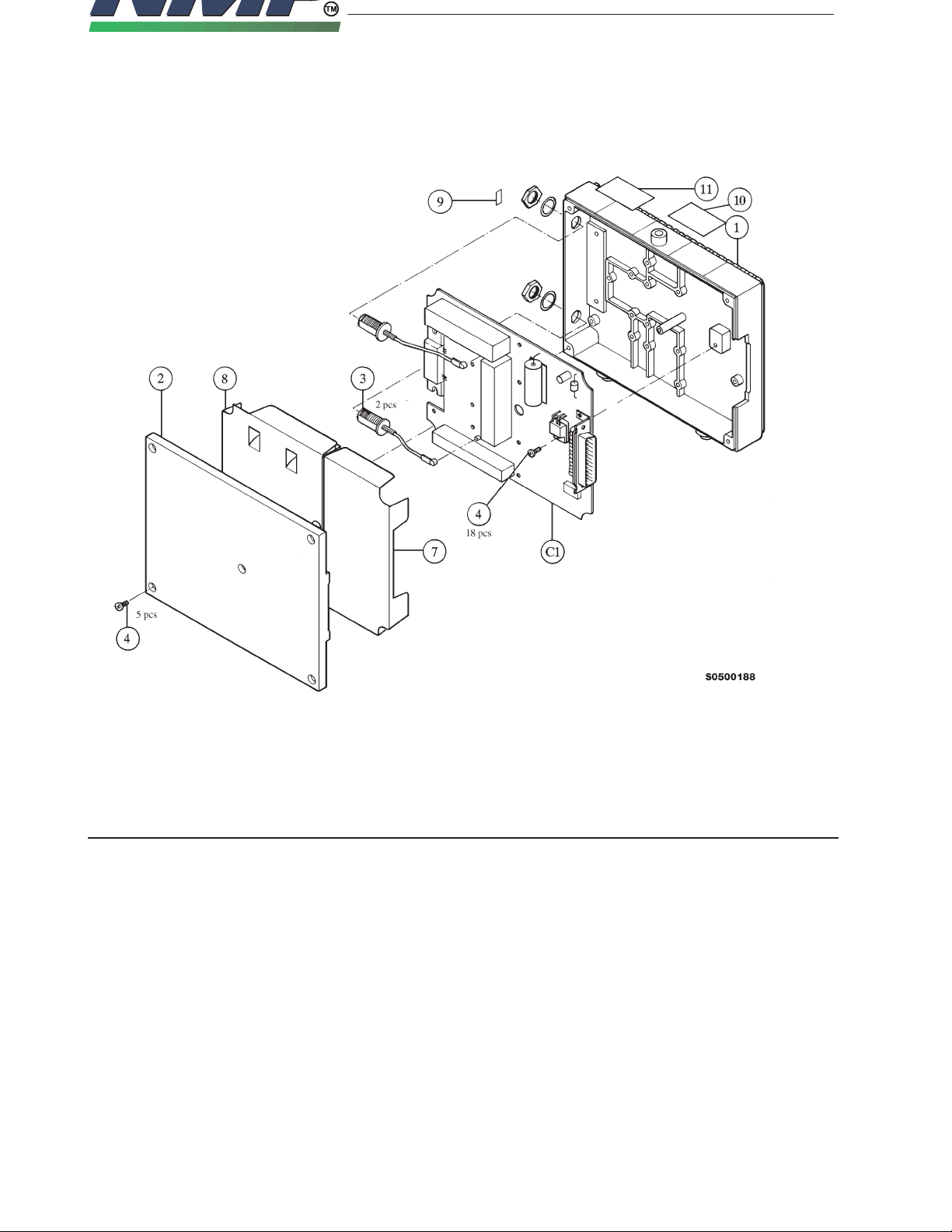
Exploded view
Technical Documentation
–
Copyright Nokia Mobile Phones
Assembly parts
ITEM Q’TY CODE DESCRIPTION VALUE, TYPE
1 9537025 Chassis 1D23393 BSH–4
2 9537014 Cover 1D21207 BSH–2
3 2 9780014 Antenna cable 4C21537 NME–1
4 23 6150299 Screw M3x8 DIN7985
7 9510105 RF shield 1 2D21209
8 9510158 RF shield 2 2D23397
9 9380227 Antenna label 4D22978
10 9380304 Continuous sheet print. according 4D23551
11 9380304 Continuous sheet print. according 4D22590
C1 0200271 Booster module DB4
Page 2

9543HK
14
–
23
Technical Documentation
Copyright Nokia Mobile Phones
V107 4200917 Transistor BC848B/BCW32 npn 30 V 100 mA SOT23
V108 4202456 MosFet IRFR9020 p–ch 50 V 8 A TO252
V109 4202456 MosFet IRFR9020 p–ch 50 V 8 A TO252
V111 4200917 Transistor BC848B/BCW32 npn 30 V 100 mA SOT23
V112 4200917 Transistor BC848B/BCW32 npn 30 V 100 mA SOT23
V113 4110130 Zener diode BZX84 2 % 5.1 V 0.3 W SOT23
V114 4100567 Sch. diode x 2 BAS70–04 70V15 mA SERSOT23
V115 4110130 Zener diode BZX84 2 % 5.1 V 0.3 W SOT23
V116 4200909 Transistor BC858B/BCW30 pnp 30 V 100 mA SOT23
V117 4100567 Sch. diode x 2 BAS70–04 70V15 mA SERSOT23
V118 4200917 Transistor BC848B/BCW32 npn 30 V 100 mA SOT23
V200 4200917 Transistor BC848B/BCW32 npn 30 V 100 mA SOT23
V201 4210096 Transistor BCP54 npn 45 V 1.5 A SOT223
V202 4110130 Zener diode BZX84 2 % 5.1 V 0.3 W SOT23
V203 4110130 Zener diode BZX84 2 % 5.1 V 0.3 W SOT23
V204 4200917 Transistor BC848B/BCW32 npn 30 V 100 mA SOT23
V300 4108647 Pin diode BAR14–1 100 V SOT23
V301 4108647 Pin diode BAR14–1 100 V SOT23
V302 4210096 Transistor BCP54 npn 45 V 1.5 A SOT223
V303 4210096 Transistor BCP54 npn 45 V 1.5 A SOT223
V304 4210096 Transistor BCP54 npn 45 V 1.5 A SOT223
V305 4110130 Zener diode BZX84 2 % 5.1 V 0.3 W SOT23
V306 4110117 Zener diode BZX84 5 % 3.9 V 0.3 W SOT23
V307 4100567 Sch. diode x 2 BAS70–04 70V15 mA SERSOT23
V308 4100567 Sch. diode x 2 BAS70–04 70V15 mA SERSOT23
V400 4200909 Transistor BC858B/BCW30 pnp 30 V 100 mA SOT23
V401 4210010 Transistor BFP183 npn 12 V 65 mA 8 GHz
D200 4340024 IC, ROM MCUH8/534 QFP80A
D201 4342286 IC, EEPROM 8kx8 bit 250 ns SO28W
N100 4346996 IC, regulator 78M05 +5 V TO252AA
N200 4309061 IC, reset generator s TL7702AID SO8
N201 434H058 IC, dac 10bit plcc PM–7533 PLCC20
N202 4345540 IC, 2 x op.amp. TLC274BID SO14S
N300 4352222 IC, pow.amp. 6 W TDMA
X200 5432120 D25–conn angle m metalbracket UNC
X201 5422636 Coax–conn sfl d=2.5 50 Ω pcb
X202 5422636 Coax–conn sfl d=2.5 50 Ω pcb
7313201 Tape pad 1x12x25mm 2–sided wht
9853961 PC board DB4 117.5x152.0x1.6 d 1/pa
Page 3

9543HK
14
–
22
Technical Documentation
Copyright Nokia Mobile Phones
C208 2307816 Ceramic cap. 47 n 20 % 25 V 0805
C209 2604110 Tantalum cap. 10 µ 20 % 25 V 7.3x4.4x2.8
C210 2307816 Ceramic cap. 47 n 20 % 25 V 0805
C211 2310424 Ceramic cap. 100 p 5 % 50 V 0805
C212 2310752 Ceramic cap. 10 n 20 % 50 V 0805
C213 2310350 Ceramic cap. 27 p 5 % 50 V 0805
C300 2310350 Ceramic cap. 27 p 5 % 50 V 0805
C301 2309852 Ceramic cap. 2.7 p 0.25 % 50 V 0805
C302 2309919 Ceramic cap. 8.2 p 0.25 % 50 V 0805
C303 2309852 Ceramic cap. 2.7 p 0.25 % 50 V 0805
C304 2310350 Ceramic cap. 27 p 5 % 50 V 0805
C305 2309852 Ceramic cap. 2.7 p 0.25 % 50 V 0805
C306 2505164 Electrol. cap. 1000 µ 20 % 40 V 12.5x30mm
C307 2307816 Ceramic cap. 47 n 20 % 25 V 0805
C308 2310350 Ceramic cap. 27 p 5 % 50 V 0805
C309 2310350 Ceramic cap. 27 p 5 % 50 V 0805
C310 2310350 Ceramic cap. 27 p 5 % 50 V 0805
C311 2307816 Ceramic cap. 47 n 20 % 25 V 0805
C312 2604093 Tantalum cap. 2.2 µ 20 % 35 V 6.0x3.2x2.8
C313 2604110 Tantalum cap. 10 µ 20 % 25 V 7.3x4.4x2.8
C314 2310350 Ceramic cap. 27 p 5 % 50 V 0805
C315 2310350 Ceramic cap. 27 p 5 % 50 V 0805
C316 2310350 Ceramic cap. 27 p 5 % 50 V 0805
C317 2310350 Ceramic cap. 27 p 5 % 50 V 0805
C318 2310350 Ceramic cap. 27 p 5 % 50 V 0805
C319 2310350 Ceramic cap. 27 p 5 % 50 V 0805
C320 2310544 Ceramic cap. 1.0 n 5 % 50 V 0805
C400 2310544 Ceramic cap. 1.0 n 5 % 50 V 0805
C401 2310544 Ceramic cap. 1.0 n 5 % 50 V 0805
C402 2604110 Tantalum cap. 10 µ 20 % 25 V 7.3x4.4x2.8
C403 2310544 Ceramic cap. 1.0 n 5 % 50 V 0805
C404 2310350 Ceramic cap. 27 p 5 % 50 V 0805
C405 2310350 Ceramic cap. 27 p 5 % 50 V 0805
C406 2309919 Ceramic cap. 8.2 p 0.25 % 50 V 0805
L002 3640301 Chip coil 150 n 20 % Q=30/25 MHz 1210
L100 3606664 Choke 30 µ
L101 0164030 Choke 9 µ
B200 4500822 Crystal 11.0592 M CL30PF h=3.6mm
Z300 4508208 Duplexer AMPS
Z309 4508372 Hz–6/a25/TX–filt 824–849 MHz AMPS
Z310 4508368 Hz–6/a25/RX–filt 869–894 MHz AMPS
V100 4100218 Trans. supr. LDP24A 100 V 30A/40 ms AG
V101 4110130 Zener diode BZX84 2 % 5.1 V 0.3 W SOT23
V102 4200917 Transistor BC848B/BCW32 npn 30 V 100 mA SOT23
V103 4202456 MosFet IRFR9020 p–ch 50 V 8 A TO252
V104 4100567 Sch. diode x 2 BAS70–04 70V15 mA SERSOT23
V105 4107027 Zener diode BZX84 5 % 16 V 0.3 W SOT23
V106 4200917 Transistor BC848B/BCW32 npn 30 V 100 mA SOT23
Page 4

9543HK
14
21
Technical Documentation
Copyright Nokia Mobile Phones
R221 1413603 Chip resistor 47 k 5 % 0.063 W 0805
R222 1413635 Chip resistor 100 k 5 % 0.063 W 0805
R223 1412430 Chip resistor 10 k 5 % 0.063 W 0805
R300 1413924 Chip resistor 220 5 % 0.063 W 0805
R301 1413836 Chip resistor 47 5 % 0.063 W 0805
R302 1413924 Chip resistor 220 5 % 0.063 W 0805
R303 1413836 Chip resistor 47 5 % 0.063 W 0805
R304 1413836 Chip resistor 47 5 % 0.063 W 0805
R305 1412335 Chip resistor 1.0 k 5 % 0.063 W 0805
R306 1411669 Chip resistor 22 5 % 0.063 W 0805
R307 1411669 Chip resistor 22 5 % 0.063 W 0805
R308 1411669 Chip resistor 22 5 % 0.063 W 0805
R309 1411669 Chip resistor 22 5 % 0.063 W 0805
R310 1411669 Chip resistor 22 5 % 0.063 W 0805
R311 1411669 Chip resistor 22 5 % 0.063 W 0805
R312 1412335 Chip resistor 1.0 k 5 % 0.063 W 0805
R313 1412409 Chip resistor 1.5 k 5 % 0.063 W 0805
R314 1412409 Chip resistor 1.5 k 5 % 0.063 W 0805
R315 1412423 Chip resistor 4.7 k 5 % 0.063 W 0805
R316 1413635 Chip resistor 100 k 5 % 0.063 W 0805
R317 1412261 Chip resistor 100 5 % 0.063 W 0805
R318 1413635 Chip resistor 100 k 5 % 0.063 W 0805
R400 1412430 Chip resistor 10 k 5 % 0.063 W 0805
R401 1412423 Chip resistor 4.7 k 5 % 0.063 W 0805
R402 1413924 Chip resistor 220 5 % 0.063 W 0805
R403 1412416 Chip resistor 2.2 k 5 % 0.063 W 0805
R404 1413924 Chip resistor 220 5 % 0.063 W 0805
R405 1411669 Chip resistor 22 5 % 0.063 W 0805
R406 1413924 Chip resistor 220 5 % 0.063 W 0805
C100 2307816 Ceramic cap. 47 n 20 % 25 V 0805
C101 2505164 Electrol. cap. 1000 µ 20 % 40 V 12.5x30mm
C102 2307816 Ceramic cap. 47 n 20 % 25 V 0805
C103 2307816 Ceramic cap. 47 n 20 % 25 V 0805
C104 2307816 Ceramic cap. 47 n 20 % 25 V 0805
C105 2307816 Ceramic cap. 47 n 20 % 25 V 0805
C106 2505261 Electrol. cap. 220 µ 20 % 25 V 8.5x11.5
C107 2310544 Ceramic cap. 1.0 n 5 % 50 V 0805
C108 2310424 Ceramic cap. 100 p 5 % 50 V 0805
C109 2310456 Ceramic cap. 180 p 5 % 50 V 0805
C110 2310424 Ceramic cap. 100 p 5 % 50 V 0805
C200 2604110 Tantalum cap. 10 µ 20 % 25 V 7.3x4.4x2.8
C201 2604110 Tantalum cap. 10 µ 20 % 25 V 7.3x4.4x2.8
C202 2307816 Ceramic cap. 47 n 20 % 25 V 0805
C203 2604209 Tantalum cap. 1.0 µ 20 % 16 V 3.2x1.6x1.8
C204 2307816 Ceramic cap. 47 n 20 % 25 V 0805
C205 2604209 Tantalum cap. 1.0 µ 20 % 16 V 3.2x1.6x1.8
C206 2310350 Ceramic cap. 27 p 5 % 50 V 0805
C207 2310350 Ceramic cap. 27 p 5 % 50 V 0805
–
Page 5

9543HK
14
20
Technical Documentation
Copyright Nokia Mobile Phones
Parts list of DB4
ITEM CODE DESCRIPTION VALUE TYPE
R077 1412335 Chip resistor 1.0 k 5 % 0.063 W 0805
R100 1412536 Chip resistor 22 k 5 % 0.063 W 0805
R101 1412430 Chip resistor 10 k 5 % 0.063 W 0805
R102 1412536 Chip resistor 22 k 5 % 0.063 W 0805
R103 1412430 Chip resistor 10 k 5 % 0.063 W 0805
R104 1412430 Chip resistor 10 k 5 % 0.063 W 0805
R105 1413635 Chip resistor 100 k 5 % 0.063 W 0805
R106 1412430 Chip resistor 10 k 5 % 0.063 W 0805
R107 1412430 Chip resistor 10 k 5 % 0.063 W 0805
R108 1412423 Chip resistor 4.7 k 5 % 0.063 W 0805
R109 1412536 Chip resistor 22 k 5 % 0.063 W 0805
R110 1412430 Chip resistor 10 k 5 % 0.063 W 0805
R111 1412310 Chip resistor 470 5 % 0.063 W 0805
R112 1412261 Chip resistor 100 5 % 0.063 W 0805
R113 1412409 Chip resistor 1.5 k 5 % 0.063 W 0805
R114 1412430 Chip resistor 10 k 5 % 0.063 W 0805
R115 1412261 Chip resistor 100 5 % 0.063 W 0805
R116 1412261 Chip resistor 100 5 % 0.063 W 0805
R117 1413635 Chip resistor 100 k 5 % 0.063 W 0805
R118 1412335 Chip resistor 1.0 k 5 % 0.063 W 0805
R119 1413635 Chip resistor 100 k 5 % 0.063 W 0805
R120 1413635 Chip resistor 100 k 5 % 0.063 W 0805
R200 1413635 Chip resistor 100 k 5 % 0.063 W 0805
R201 1413603 Chip resistor 47 k 5 % 0.063 W 0805
R202 1413603 Chip resistor 47 k 5 % 0.063 W 0805
R203 1412335 Chip resistor 1.0 k 5 % 0.063 W 0805
R204 1413635 Chip resistor 100 k 5 % 0.063 W 0805
R205 1413635 Chip resistor 100 k 5 % 0.063 W 0805
R206 1413603 Chip resistor 47 k 5 % 0.063 W 0805
R207 1412536 Chip resistor 22 k 5 % 0.063 W 0805
R208 1412430 Chip resistor 10 k 5 % 0.063 W 0805
R209 1412430 Chip resistor 10 k 5 % 0.063 W 0805
R210 1413603 Chip resistor 47 k 5 % 0.063 W 0805
R211 1413603 Chip resistor 47 k 5 % 0.063 W 0805
R212 1413603 Chip resistor 47 k 5 % 0.063 W 0805
R213 1413603 Chip resistor 47 k 5 % 0.063 W 0805
R214 1412423 Chip resistor 4.7 k 5 % 0.063 W 0805
R215 1800673 NTC resistor 15 k 10 % 0.12 W 0805
R216 1412536 Chip resistor 22 k 5 % 0.063 W 0805
R217 1412430 Chip resistor 10 k 5 % 0.063 W 0805
R218 1412536 Chip resistor 22 k 5 % 0.063 W 0805
R219 1412430 Chip resistor 10 k 5 % 0.063 W 0805
R220 1413603 Chip resistor 47 k 5 % 0.063 W 0805
–
Page 6
9543HK
14
19
Technical Documentation
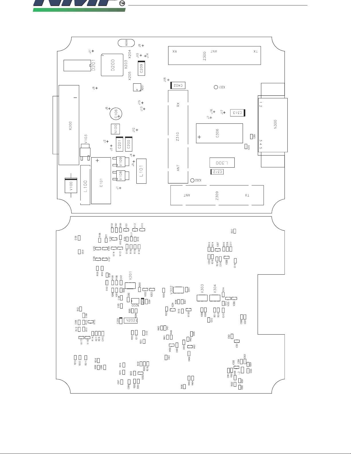
Layout diagrams of DB4
–
Copyright Nokia Mobile Phones
Page 7

9543HK
14
18
Technical Documentation
Circuit diagram of transmitter section
–
Copyright Nokia Mobile Phones
Page 8

9543HK
14
17
Technical Documentation
Circuit diagram of CPU section
–
Copyright Nokia Mobile Phones
Page 9

9543HK
14
16
Technical Documentation
External signals to internal signals
–
Copyright Nokia Mobile Phones
Page 10

9543HK
14
15
Technical Documentation
Circuit diagram of receiver section
–
Copyright Nokia Mobile Phones
Page 11

9543HK
14
14
Technical Documentation
Copyright Nokia Mobile Phones
RF and baseband interconnection and external connections
–
Page 12

9543HK
14
13
Technical Documentation
Power Distribution Diagram
–
Copyright Nokia Mobile Phones
Page 13

9543HK
14
12
Block Diagram
Technical Documentation
–
Copyright Nokia Mobile Phones
Page 14

9543HK
14
11
Control logic
Control logic consists of the MBUS buffer and BENA receiver. MBUS transmitting is buffered via transistors V111 and V112. R119 and R117 are collector resistors, V114 is a protection diode for the situation when the cpu has no power.
This diode prevents the pull–down of the MBUS during power down. R115,
C110 and R116 are protection components. V113 is used to prevent negative
voltages entering to the rx–line and to limit the max voltage to 5.1 V.
BENA is used to control the ramp start and stop. In handportable side there is
an open collector transistor used to pull the line down. The current flowing to
the line will switch on the transistor V116 via resistor R111. The transistor will
conduct and the OBENA line will go up. The switching point is 6mA and the
short circuit current is 8 mA, set with the R111 and R112.
Capasitor C108 and zener V115 are used for overvoltage protection. R113,
C109 are used to compensate overshoot due to long BENA line. R112 is on
current treshold control. V117 avoids reverse leakage current at booster off
state.
Technical Documentation
–
Copyright Nokia Mobile Phones
Page 15

9543HK
14
10
If there is any voltage from the detector, the cpu will shut off the mosfets V108
and V109 and so the bias–supply of the PA module. Then it will inform the
handportable about the situation.
Power supply logic
Power supply logic has following subparts: power on logic, overvoltage protection, 5 V regulator for logic, 9 V regulator for the analog section, power switch
for PA.
The battery voltage V+ comes through connector X200. The transzorb V100
limits the voltage to max. 31 V. L1 is used to limit transient pulses and C100
and C101 will smooth possible variations of the voltage.
Power on logic consists of transistor V102, resistors R100–R102, C102 and
zener V101. The VC line from the connector goes from zero to +5 V, when the
handportable is connected. The transistor V102 pulls the mosfet V103 gate to
ground and V103 conducts. This will turn on the power line VBATT and provide
the voltage to other regulators. R103 is used to keep the mosfet off when the
V102 does not conduct.
Technical Documentation
–
Copyright Nokia Mobile Phones
PA module has its own power switch V108 and V109. CPU can control the
switch using the control line TXENA. When the TXENA is high, V107 will conduct and turn on V108 and V109. Coil L101 is used to prevent the rf power
feedthrough from the PA module.
Supply voltage to PA module should be under 16V. Overvoltage protection for
the module is built using zener V105, diode V104, transistor V106 and resistors
R77, R106. When the input voltage rises over 16V the zener V105 start to conduct and open the transistor V106 in V107 base. The V107 stops conducting
and shuts down V108 and V109. This will cut off the bias power supply from
the PA–module during the overvoltage time.
The CPU can control the 8 V bias voltage of the PA module with PSWITCH
control line. When the PSWITCH is high the transistor V118 will conduct and
pull down the VB2OFF line. This will shut down the the 8 V bias voltage regulators V303 and V304. The bias voltage switch down can be speeded up by
switching the V302 on using the VB2DOWN–line.
The CPU can measure the VBATT voltage via A/D converter using resistive divider R108/R109 and C107 and decide if the voltage level has been out of limits for too long time. It this is so the CPU will inform the handportable about the
situation. The voltage limits and the timing values are stored in EEPROM.
Logic 5 V is generated by the regulator N100 and C104–C106. The input to the
regulator is taken after mosfet V103 and so the logic voltage is cut off when the
VC line goes 0. The average current consumption of the logic is 5.4 mA.
The 9.6 V regulator is used to power the analog section of the booster. It consists of the two zeners V202 and V203, transistor V201, resistor R203 and condensators C200–C202.
The total current consumption when the VC line is off is under 100uA.
Page 16

9543HK
14
–
9
Technical Documentation
Copyright Nokia Mobile Phones
EEPROM D201 is connected to ports P5 (data) , P3 ,P1 (address) and P6
(control). Resistors R211–R213 are used to ensure that the control lines are in
inactive state during reset.
The CPU has an internal A/D converter wich is used to measure temperature, rf
output power and voltage levels.
The reset generator IC TL7702AID and one quarter of the opamp N202 are
used to generate 5.06 V reference voltage for the A/D, to NTC resistor R215,
and to the D/A converter. The 2.53 V reference voltage from the N200 is amplified to 5.06 V using one quarter of N202 and two resitors R204 and R205. This
voltage is fed to the A/D converter reference pin (cpu pin 60). This voltage is
also scaled down to 1.58 V with resistors R216, R217 and buffered with one
quarter of the N202 for the D/A converter N201.
The CPU uses an D/A converter to set the pin diode current to wanted level.
Because only positive voltages were available, the D/A converter N201 is connected to voltage mode. Reference voltage goes to the pin 2 and output is from
the pin 19. Because of the operation mode, the reference voltage must not be
much over 1.5 V or the linearity suffers. Reference voltage is buffered with
one quarter of N202 because the D/A needs a low impedance source.
The D/A converter will output a voltage which is dependent of the digital input
word. When the input word is zero the output is zero volts, and when the input
is max, the output is at the reference voltage. By changing the input words with
CPU the ramp of the output voltage can be controlled. The output voltage is fed
via RC filter R222 and C211 to the positive input of one opamp of N202. The
time constant of the integrator is 10us and it is used to remove noise from the
output voltage of the D/A.
The output power of the PA module is measured with the power detector V308.
Voltage from the power detector is buffered in one amplifier of N202. From
there it is fed via resistive divider R218–R220 to the integrator‘s negative input.
Divider divides the RF input voltage by 2.66 to scale it to same level as the DA–
converter output voltage. Integrator time constant is defined by the capacitor
C212 and resistor R221.
Error voltage from the integrator is fed via R223 to the emitter follower V204
and from there to the pindiode attenuator. Emitter follower is used to boost the
current drive. C213 is used to attenuate possible rf voltages coming from the
pin diode attenuator.
Temperature is measured with NTC resistor R215, resistor R214 and CPU ad–
channel 5.
R203 provides biasing for V201. Transistor V201 regulates the voltage with
V202 and V203.
If for some reason the PA module has power output without BENA line enabling it, the cpu should switch the RF module off. The power cutoff logic is made
with internal A/D converter . One quarter of N202 is continuously monitoring the
output voltage of the power detector and feeds it to the A/D converter. When
the BENA line is inactive, the cpu reads continuously the power output via A/D.
Page 17

9543HK
14
8
C309–C312 are RF bypass capasitors for the PA module’s power lines. C306 is
energy storing capasitor for digital mode switcing transients. C317–C319 are
RF bypass capasitors for power detector. C316 prevents detected dc voltage
shortcircuit to ground via directional coupler.
Microstriplines and coils:
Z301 and Z302 are PIN diode attenuator matching lines. Z303 is ground return
line for the PIN diode current and also resonating with C305. Z304 is 50 ohm
interconnection line from the attenuator to the PA module. Z305 is 50 ohm interconnection line from the PA module to the directional coupler. Z306 and
Z307 forms the directional coupler. Z308 is 50 ohm interconnection line from
the coupler to duplexer Z309. Z311 is connecting duplexer Z310 antenna output to duplexer Z309 and the antenna output pin of X202. L2 is compensating
the internal capasitances of the PIN–diodes and thus improving the dynamic
range of the attenuator. L101 prevents RF harmonics leaking outside of mechanics.
RF power control logic
Technical Documentation
–
Copyright Nokia Mobile Phones
RF power control logic consist of H8/534 CPU D200 and several IO–devices.
Crystal B200 and capacitors C206 and C207 build an oscillator (11.05692 MHz)
for the CPU. IC N200, resistor R206 and capacitor C204 are used to start up
the CPU. IC N200 constantly monitors +5 V and +9.6 V signals, and if there are
any dropouts it will pull down the reset line and keep it there until the voltages
have rised again and after adjustable delay made with C203.
Capasitor C204 is used to prevent the oscillations of the reset line. R206 will
pull up the reset line because the TL7702 has an open collector output. Resistor R210 is used to pull up the NMI–line.
Communication with the handportable is done via MBUS. Received MBUS signal is fed through protection circuit to the serial input of the processor pin 67.
The MBUS signal is inverted via R201–R202 and V200 for the internal timer input in CPU pin 46. The CPU can use this input to determine when the MBUS
has no traffic. Signal is inverted because the timer only reacts to rising edge of
the signal and it is better to get the indication right from the startbit.
Transmitted power is controlled by the pindiode attenuator in RF section. The
attenuation factor is controlled by the CPU via 10 bit D/A converter N201. It is
connected to CPU ports P2 and P4. P4 has the 8 lsb address bits and P2 the
upper 2 bits. During operation when the CPU finds rising edge in BENA line it
will start delay and after the delay has elapsed will start feeding the D/A with
rising values until the needed power level has been achieved.
8k*8bit EEPROM is used to store necessary constants for output levels, attenuation factors and timing factors. The CPU can read and write the EEPROM via
its ports. To protect the data, EEPROM is divided to two blocks and both have
the same data and checksum. The EEPROM is written only during the calibration.
Page 18

9543HK
14
7
Power amplifiers
Transmitted constant level signal from handportable TRX is routed via duplexer
Z300 to fixed attenuator pad. Then signal goes through the voltage controlled
variable PIN diode attenuator. This stage has about 38 dB control range and it
takes care of the power ramping and desired power level setting in both analog
and digital modes. After that the signal is fed to power amplifier module, which
has 37 dB gain. Its maximum output power is +38 dBm. The module can be
switched to isolating state by switching off Vbias in PA modules pin 2. This is
done with signal VB2OFF. During rampdown PA bias capasitor C313 is discharged with V304 by signal VB2DOWN. During false transmission or with
overvoltage the power supply line for PA module is switched off. After PA module a small portion of output power is picked by the power detector with a directional coupler. Power detector is heavily forward biased to increase linearity.
Output voltage from detector is limited by means of shunt diode switch. After
the directional coupler the signal is fed to the antenna via output duplexer
Z309. A separate 8V regulator for PA module bias voltage maintains performance with varying battery voltages.
Technical Documentation
–
Copyright Nokia Mobile Phones
Semiconductors:
V301 and V300 are PIN diodes for variable attenuator. V303 and V304 are reg-
ulator transistors for power amplifier bias voltage, they can be switched off by
setting VB2OFF to 0 V. V302 is discharging switch for C313. It can be activated by setting VB2DOWN to 5V. V305 and V306 provide reference voltage
for V303 and V304. V308 is Schottky diode pair for power detector rectifier.
V307 is Schottky diode pair for detected voltage limiter.
Resistors:
R300 ...R302 form fixed PI attenuator. R303 and R304 are matching resistors
in variable attenuator. R312 gives bias current for V303 and V304 base and for
zener diodes V305 and V306. R317 is matching resistor for the directional coupler. R315 is power detector’s voltage divider’s upper resistor. R314 is power
detector’s voltage divider’s lower resistor, which comes in action only when detected voltage exceeds 0.6 volts thus opening the diodes in V307. R316 is basic load for power detector. R318 and R313 sets 0.3 volt forward bias for power
detector diodes. The same potential is fed to other end of R314 to prevent
backward biasing during high power levels. R308–R311 are current limiting resitors for the bias regulator transistors. R306, R307 are collector current limiting
resistors for V302. R305 is base current limiter for V302.
Capasitors:
C300 and C304 are DC block capasitors to prevent PIN–diode current to be
shorted via coil L2. C301–C304 are PIN–diode attenuator matching capasitors.
C305 is resonating with Z303 and thus improving attenuator matching to PA
module. C307 and C308 are supply bypass capasitors to PA module 8 V bias
voltage. C313 smooths the rising and falling transients during power ramping
and thus limits the transmitted spectrum spread. C314 and C315 are RF bypass capasitors for V303 and V304.
Page 19

9543HK
14
6
Functional Description
Circuit Description
The heart of the control logic is the Hitachi H8/534 microcontroller running
11.0592 MHz. It adjusts the output power accordingly to a given power level
and temperature. The controller also monitores TX output power and can
switch power off from the power amplifier if any false transmission is detected.
Output power is ramped up and down under CPU control, CPU outputs the
ramp values to external 10 bit D/A converter.
An external EEPROM is used to store factory tuning values and other data. The
data in EEPROM is secured by checksum and double copy.
The CPU also takes care of all the timing functions. When it receives the TX
enable signal (BENA), it starts an adjustable delay and then ramps up the TX
power to level given by the handportable via MBUS. When the TX enable signal
is removed a new adjustable delay is started and at the end of it, TX power is
ramped down. Both delays are adjustable and stored in EEPROM. Nominal
delay values are 623 µs for ramp up and 123 µs for ramp down.
Technical Documentation
–
Copyright Nokia Mobile Phones
Receiver
Received signal from antenna connector is routed via RX– duplexer Z310 to
low noise linear RF amplifier, which has 14 dB gain and 1.8 dB noise figure.
Full gain for booster RX path is specified to ca.7 dB. This way it is possible to
maintain transceiver RX sensitivity. The dc power for the amplifier is fed from
regulated 9.6 V supply and the amplifier has active biasing to maintain performance during battery voltage variations. After amplification signal is fed to
handportabe TRX via pi–attenuator and duplexer Z300.
Semiconductors:
V401 is low noise linear RF amplifier. V400 provides constant current to V401.
Resistors:
R403 feeds base bias for V401. R402 is current sensing resistor for active bias
feedback loop. R400 and R401 sets base voltage for V400 and thus collector
voltage for V401. R404 –R406 forms pi–attenuator to set module gain to right
value.
Capasitors and microstriplines:
C405 is DC blocking capasitor to prevent the base voltage of the V401 to be
shorted to ground via duplexfilter. C406 is matching the output impedance of
the V401 to 50 ohm input impedance of duplexer. C404, C403 and C401 are
RF bypass capasitors. C400 is stabilizing the active bias feedback loop. C402
is filtering the power supply line. Z402 is part of output impedance matching of
the V401. It also feeds dc power to the V401. Z400 and Z403 are 50 ohm
transmission lines to connect the amplifier to duplexers. Z401 acts as interconnection line between C405 and the base of V401.
Page 20

9543HK
14
5
RF_IN connector, X201
Pin Symbol Description
1 RF_IN Input to input duplexer
2 GND Ground connection
RF_OUT connector, X202
Pin Symbol Description
1 RF_OUT Output from output duplexer
2 GND Ground connection
Technical Documentation
Copyright Nokia Mobile Phones
• min./typical/max. +10 dBm/+14 dBm/+16 dBm
• DC connected to ground via duplexer
• min./max. +6.8 dBm/+34.8 dBm
• DC connected to ground via duplexer
–
Internal Signals and Connections
Internal signal names between RF and logic modules
TXENA PA module power control signal
PSWITCH control line to bias switch transistor
TX Serial bus from CPU
RX Serial bus to CPU
VBATT logic and analog main supply.
VBIAS main supply to PA–module
PWR_GOOD power supply voltage monitoring line
VB2OFF PA–module bias switch off signal
OBENA control signal to CPU timer input capture register.
RF_POWER output signal from rf–detector
PINCURR control signal to pin diode attenuator
FRDUPL input signal from input duplexer to rf input amplifier
TODUPL output signal from rf amplifier to output duplexer
VB2DOWN bias voltage pulldown control.
After handportable is put into the cradle it will display booster connected indication for few seconds.
Page 21

9543HK
14
4
Technical Documentation
Technical Specifications
Modes of Operation
The module has two operation modes, analog and digital.
External Signals and Connections
ConnectorNotes Description
name
X200 System connector, D25 Control signals from handportable
X201 RF_IN, mini–UHF type RF signal from handportable
X202 RF_OUT, mini–UHF type RF signal to antenna
Sytem Connector, X200
Pin Symbol Description
–
Copyright Nokia Mobile Phones
3 GND Battery ground connection
• typical/nominal 0 V
4 +V Battery voltage supply
• min./typical/max. +10.0 V/+12.5 V/+16.0 V
6 VC Main on/off switch voltage
• min./max. 0 V/+5 V
• >5 V switches booster on
7 BENA Control signal to switch booster transmitter on/off
• min./typical/max. 0 mA/6 mA/8 mA
• current controlled, 200 Ω to +3 V, Switch on
current 6 mA, max short circuit current 8 mA
12 M2BUS Communication bus to booster
• 100k to +5 V, 200 Ω in series
16 +V Battery voltage supply
• min./typical/max. +10 V/+12.5 V/+16.0 V
17 GND Battery ground connection
• typical 0 V
24 GND Battery ground connection
• typical 0 V
Page 22

9543HK
14
3
Basic Specifications
Cellular system North American Dual–mode
TX frequency band 824.010,...848.970 MHz
RX frequncy band 869.010,...893.970 MHz
Power class 1
Maximum output power 3 W
Power supply voltage 10.5,...16 V
Current consumption, stand by < 0.1 mA
Current consumption, analog mode trans. 2.5 A (full power)
Current consumption, digital mode trans. 1.5 A (full power)
List of Submodules
The booster does not contain separate submodules. It can be divided into receiver, power amplifier, power control logic and power supply logic.
Technical Documentation
–
Copyright Nokia Mobile Phones
Page 23

9543HK
14
2
Technical Documentation
Introduction
Technical Summary
RF booster is an accessory device to increase handportable tranceiver transmit
power. Handportable is a power class IV transceiver. Booster is built for power
class I. Modes of operation are analog and digital. Booster contains also a RF
preamplifier for handportable receiver.
Necessary control logic is included. Main functions of the logic are: TX power
control and compensation. Control logic is conneted to handportable via MBUS
and two control lines. TX power ramp–up and ramp–down timing is controlled
using control line BENA.
List of Modules and parts of RF booster
Dual mode RF booster BSH–4 0500188
RF booster module DB4 0200271
Assembly parts MBSH–4 0260286
Booster cable SCE–8 9780091
D25 extension cable SCE–9 9780083
RF extension cable XRH–1 9780039
Mounting bracket booster MBM–3 0700016
–
Copyright Nokia Mobile Phones
BSH–4
MBM–3
SCE–8
Page 24

9543HK
14
1
Contents
Introduction 14–2
Technical Summary 14–2
List of Modules and parts of RF booster 14–2
Basic Specifications 14–3
List of Submodules 14–3
Technical Specifications 14–4
Modes of Operation 14–4
External Signals and Connections 14–4
Internal Signals and Connections 14–5
Functional Description 14–6
Circuit Description 14–6
Block Diagram 14–12
Power Distribution Diagram 14–13
RF and baseband interconnection and external connections 14–14
Circuit diagram of receiver section 14–15
External signals to internal signals 14–16
Circuit diagram of CPU section 14–17
Circuit diagram of transmitter section 14–18
Layout diagrams of DB4 14–19
Parts list of DB4 14–20
Exploded view 14–24
Assembly parts 14–24
Technical Documentation
–
Copyright Nokia Mobile Phones
 Loading...