

Page 1

TROUBLESHOOTING
NHC–4
Contents
Troubleshooting for Base Band 6–2–3
Overview to base band troubleshooting 6–2–3
General 6–2–4
Current consumption failures in flash station 6–2–5
Phone takes all available current 6–2–5
Phone does not take current at all 6–2–5
Current consumption OK during power–up, then fail 6–2–5
Troubleshooting Diagram; Flash Programming OK, part 1 6–2–7
Troubleshooting Diagram; Flash Programming OK, part 2 6–2–8
Troubleshooting Diagram; Flash Programming OK, part 3 6–2–9
Troubleshooting Diagram; Flash Programming OK, part 4 6–2–10
Troubleshooting Diagram; PWR Button Fault 6–2–11
Troubleshooting Diagram; Display Selftest Failed 6–2–12
Troubleshooting Diagram; Audio Fault 6–2–13
Power Up Sequency Diagram 6–2–14
Repairing Instructions for Flash Faulty Units 6–2–15
Calib BATT_VOLTAGE = 6.0 V 6–2–16
Calib CHARGE_VOLTAGE = 6.0 V 6–2–16
Troubleshooting Diagram; Power Up and MCU Selftest Malfunctions 6–2–17
Power Up Malfunction 6–2–18
Troubleshooting Diagram; Power Up Malfunction 6–2–21
Troubleshooting Diagram; MCU Selftests Malfunction 6–2–22
Troubleshooting for RF 6–2–23
The Red Line of this Repair Guide 6–2–23
Alignment Stage References 6–2–23
Final Stage References 6–2–24
How to read those sheets? 6–2–25
ERROR A10; The DUT does not turn on 6–2–27
ERROR A13a; AFC tuning fails 6–2–29
ERROR A13b; UHF Synthesizer 6–2–30
ERROR A13c; VHF Synthesizer 6–2–31
ERROR A20; Fail in Bias Control tuning 6–2–32
ERROR A22–57a; Fail in power level table 6–2–35
ERROR A22–57b; Fail in power level table, part II 6–2–38
ERROR A22–57c; Fail in power level..., part III 6–2–40
ERROR A22–57d; Fail in power level..., part IV 6–2–42
ERROR A66; RX audio gain tuning fail 6–2–44
ERROR A67; SINAD – fail 6–2–45
ERROR A68; RSSI – level fail 6–2–47
9526ARo
Technical Documentation
6–2–1
Copyright Nokia Mobile Phones
Page 2

TROUBLESHOOTING
NHC–4
9526ARo
Technical Documentation
Copyright Nokia Mobile Phones
6–2–2
ERROR A69–70; Tuning ST/audio deviation 6–2–48
ERROR A72; The I/Q Tuning fails 6–2–49
ERROR A73; Digital AGC tuning fails 6–2–51
ERROR A00; RF side supply voltages 6–2–53
Page 3

TROUBLESHOOTING
NHC–4
9526ARo
Technical Documentation
Troubleshooting for Base Band
Overview to base band troubleshooting
The purpose is to define fault block of the module and then find out the defect
component.
Baseband oriented failures are usually found out in the flash station of the production line.In the first phase,before programming the flash,the phone is started
to minimum mode and current consumption is measured.If current consumption
is in acceptable limits and MBUS registration is OK,flash is programmed.After
flash programming phone is started to local mode and tester starts to send
MBUS messages to activate MCU self tests.During the MCU self tests all the
major components of the baseband are tested.Every test returns number of the
test and result ( OK / failed ).All information of the test is stored to phone oriented test file,witch is available on the troubleshooting station.MCU self tests
can be restarted on trobleshooting station with SERVICE PCLOCALS.
If phone can be flashed and all/some self tests performed,the baseband is
mainly OK.By refering the test file of the phone,defect component or connections between components can located.
6–2–3
Copyright Nokia Mobile Phones
In case of current consumption/MBUS registration failure,the phone must be
taken to more specific measurements of voltages,clocking signals and states of
reset signals.
Page 4

TROUBLESHOOTING
NHC–4
General
9526ARo
Technical Documentation
Copyright Nokia Mobile Phones
6–2–4
The purpose is to define fault block of the module and then find out the broken component. The trouble shooting diagram has been planned so that the fault, whatever
it is, can be found by as simple measurements as possible.
The flow diagrams give you the overview of the blocks. The purpose is that you
proceed through the flow diagram so that, if your answer is YES for the asked
question, go straight to the next level, but if your answer is NO, you have to go
the subbranch.
Required servicing equipment:
– PC for PC locals
– Power supply (2.0 A)
– Digital multimeter
– Oscilloscope
– Modular cable
– RS232/MBUS adapter
Page 5

TROUBLESHOOTING
NHC–4
9526ARo
Technical Documentation
Current consumption failures in flash station
Current consumption can fail in three ways in flash station.Typical to all these
failures is,that phone can not be programmed or tested via MBUS.The most
common failure is that phone takes almost normal current during startup and
after couple of seconds all circuits are powered down.Reason for this failure is
in power–,clock– or reset distripution of the phone.In cases where phone does
not take current at all or phone takes all available current the reason is usually
defected power ASIC PSL+ (N100) or bad soldering ( short or open ) around
PSL+ .
Phone takes all available current
If phone takes all available current,the reason for failure can be detected by:
– visual check of bad solderings in PSL+ (N100) , components around it and
bottom connector X1
– cheking ,if transistors V908,V910 and V911 in TX block are defected
6–2–5
Copyright Nokia Mobile Phones
Phone does not take current at all
If phone does not take current at all,check following things:
– solderingins of PSL+
– VBATT voltage should be available in pins 5 and 20 of PSL+
If connections of PSL+ are OK and VBATT in pins 5/20 is OK, change defected
power ASIC N100
Current consumption OK during power–up, then fail
The most common situation in current consomption failures is,that phone starts
almost normally,but after few seconds all circuits are powered down.The power–down is normally caused by lack of watch–dog signal from MCU to
PSL+.There are three major things to be checked in this kind of failure situation.First,check power distribution to all main components of baseband.Then
check that clock is delivered to ASIC,DSP,MCU,RFI and AUDIO CODEC.If everything is OK so far,check RESET status of circuitry mentioned above.
Cheking the power distribution of baseband
Before voltage measurements of the circuitry,power–down of PSL+ must be
prevented.This is done by shorting the watch–dog timing capacitor C106 with
wire soldered from one end of the cap to the other.
1.Check PSL+ output voltages from N100 pins 4,21,2,24 and 1.Expected value
is around 4.65V.Also,check voltage in N100 pin 12 (DETIN) to be 1.23V
2.Check supply voltage VL1 (4.65V) of MCU (D302) from pins 5 and 42.Check
VREF voltage from MCU pin 60.Check voltages of MCU related memory cir-
Page 6

TROUBLESHOOTING
NHC–4
9526ARo
Technical Documentation
Copyright Nokia Mobile Phones
6–2–6
cuits D300 (FLASH) pins 31 and 32,D305 (RAM) pin 28 and D307 (EEPROM)
pin 8
3.Check voltage VL1 from ASIC (D401) pins 1,36,57,73,108 and 122.Check
also supply voltage of RFC buffer (D402) from pin 5
4.Check voltage VL2 from DSP (D200) pins 8,11,36,39,49,64,76,87 and
90.Voltage should be around 4.65V.VL2 is also fed to DSP RAMs D201 and
D202 to pin 28.
5.Check voltages of RFI (N450).VL1 is fed to pins 48,52 and 60.VA1 (4.65V) is
fed via FET V450 to pins 5,10 and 13.If D450 is installed,check voltage VL1 in
pin 5.
6.Check supply voltages of AUDIO CODEC.VA2 is fed to pins 2,3 and 15 via
R159 (2R2).Voltage sould be around 4.60V.
Page 7
TROUBLESHOOTING
NHC–4
9526ARo
Technical Documentation
Copyright Nokia Mobile Phones
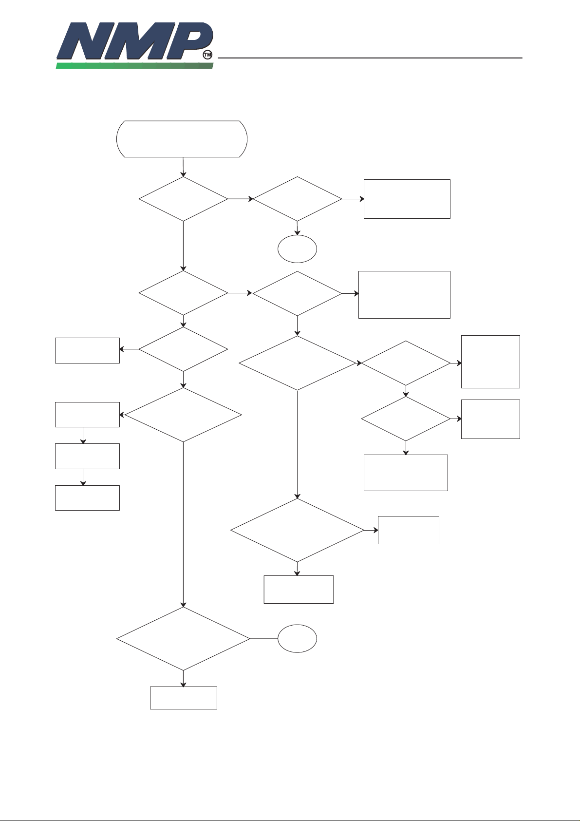
Troubleshooting Diagram; Flash Programming OK, part 1
FLASH programming OK
Check X1
C106 OK ?
YES
R100 OK ?
MBUS
registration
OK?
Power
stays on?
NO
NO
NO
VBATT
pins 5, 20?
YES
N100/XRESET/pin 8
+5 V after pwr on?
YES
YES
Display:
selftest failed
YES
3
Display:
selftest failed
YES
MBUS line X1/5
+5 V after pwr on?
YES
NO
NO
D302/MCU/pin 3
D401/ASIC/pin 56
rstrobex
Short circuits in data
data lines. data line
disconnected, VREF
unconnected
NO
R316
+ 5 V?
YES
D401 pulses
pin 91
YES
NO
pin 66/TXD
doesn’t apply
+5 V change
NO
6–2–7
If D302 at
D302
Change
ASIC
D401
YES
Change N100
Power supp. to the logic
circuits +5 V after pwr on?
NO
Change N100
MCU/D302/pin67/RDX
+5 V after pwr on (J109)?
NO
If R317 is OK
change D302
YES
2
ASIC OK
YES
Change first
D302
Page 8

TROUBLESHOOTING
NHC–4
9526ARo
Technical Documentation
Copyright Nokia Mobile Phones
Troubleshooting Diagram; Flash Programming OK, part 2
2
Change D302
YES
NO
9.72 MHz at
D302 at pin 69
NO
MCU/D302/pin 10
RESETX +5 V after
power on?
YES
9.72MHZ at MCU
/D3027pin 70
/XTAL ?
YES
NO
Change D230
6–2–8
Check D402
G580,D401
NO
9.72 MHZ at
D401 pin 70
YES
Check
R419
MCU/D302
/pin 8/MD2, MCU/D302
/pin 9/STNDBY?
+5V
YES
MCU/D302/pin43
/XPWROFF pulses up to
+5 V after pwr on?
YES
MCU/D302/pin77
/IRQ0 +5 V after
power on?
YES
MCU/D302/pin4
/WSTROBEX +5 V
after pwr on?
NO
NO
Change D302
NO
Change D302
NO
Check joints
and foils
Check D302
YES
Check all soldered joints
The data and address signals must
a clear difference between low (0 V)
and high (+5 V)
Page 9
TROUBLESHOOTING
NHC–4
9526ARo
Technical Documentation
Copyright Nokia Mobile Phones
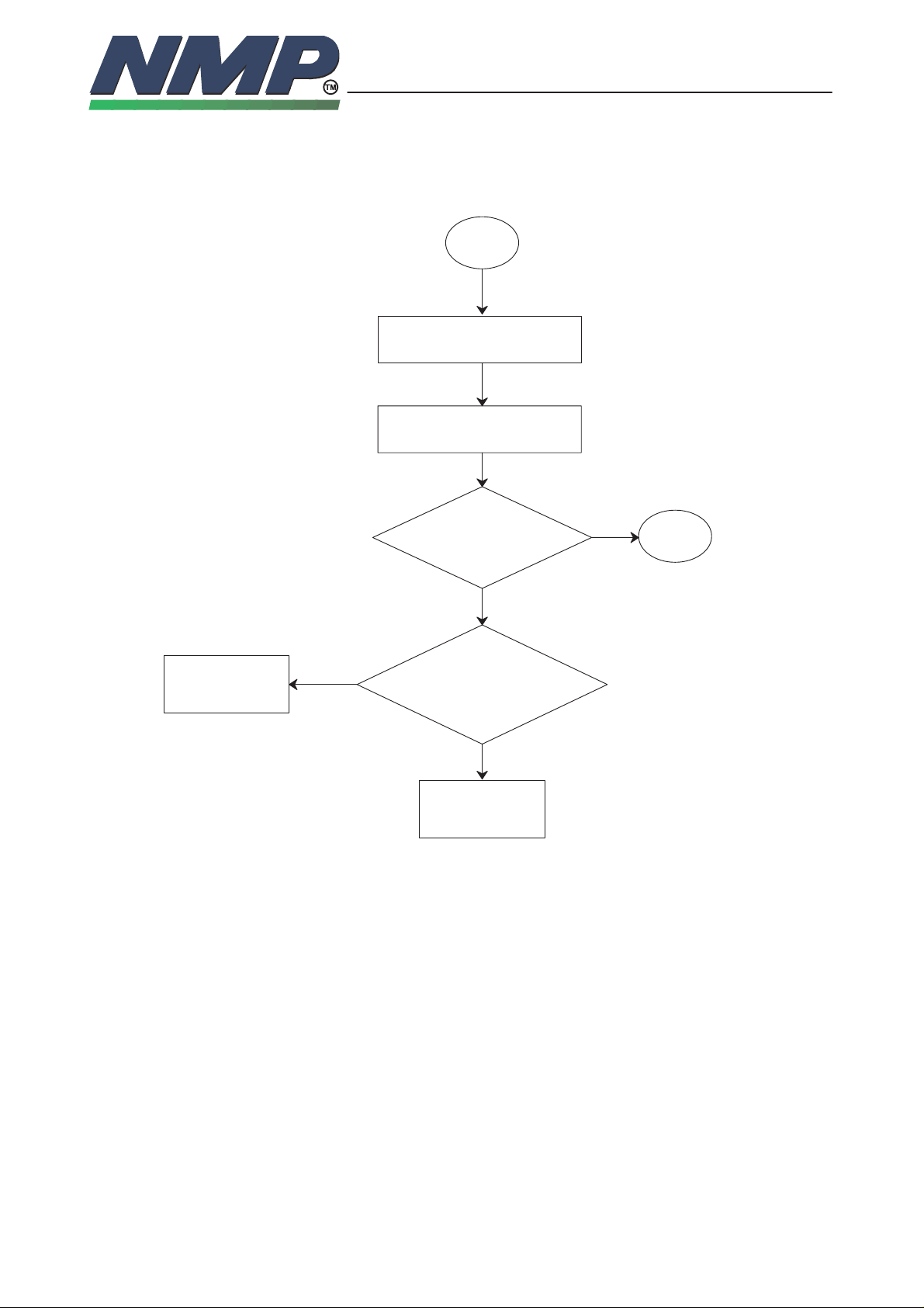
Troubleshooting Diagram; Flash Programming OK, part 3
3
MBUS registration OK?
YES
Display: selftest failed?
YES
EEPROM
initialization OK?
YES
4
6–2–9
Check D302,
R320,R321
NO
NO
D307 EEPROM
/pins 5,6/SDA/SCL pulses
+5 to 0 V during r/w
action?
YES
Change D307
Page 10

TROUBLESHOOTING
NHC–4
9526ARo
Technical Documentation
Copyright Nokia Mobile Phones
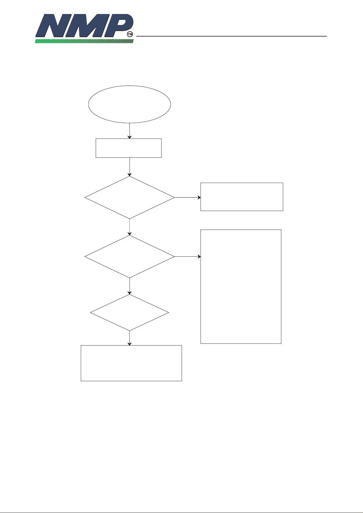
Troubleshooting Diagram; Flash Programming OK, part 4
4
D300/FLASH
/pin 11 +12 V during
programming?
YES
D302/MCU
/pin 64/HOOK/RXD2
pulses during prog?
YES
NO
NO
Check X1/pin 14
C302,L300
Check X1/pin 6
R304,R305
6–2–10
X1/pin 7
/PHFS/TXD2 pulses
during programming?
YES
D300/FLASH
/pin 12/PWD +5 V
after power on?
YES
D300/FLASH
/pin 22/ROMSELX pulses
from +5 to 0 V after
power on?
YES
D300/FLASH
/pin 24/RSTROBEX pulses
from +5 to 0 V after
power on?
NO
NO
NO
NO
Check D302/pin 63
R314
Check D302
Check D302
Check D302
Check D300/FLASH
ADDRESS/DATA LINES
/no shortcircuits or
unconnected pins allowed
OK
Change D300
YES
D300/FLASH
/pin 9/WSTROBEX pulses
from +5 to 0 V after
power on?
NO
Check D302
Page 11

TROUBLESHOOTING
NHC–4
9526ARo
Technical Documentation
Copyright Nokia Mobile Phones
Troubleshooting Diagram; PWR Button Fault
Nothing happens when
PWR button is pressed
N100/PSL+
pin 10 +5 V when
VBATT is connected
YES
NO
N100/PSL pins 2,5
6–2–11
Check
X1
NO
VBATT voltage
YES
Change
N100
Change
UI
Check
UI–conn.
N100/PSL
pin 10 +5–>0 V when
push PWR button
YES
R100,C106
OK
Check component
around N100,if OK
change N100
Page 12
TROUBLESHOOTING
NHC–4
9526ARo
Technical Documentation
Copyright Nokia Mobile Phones
Troubleshooting Diagram; Display Selftest Failed
Display selftest failed or
phone doesn’t registrate to
the system (tester)
Use PCLocals to
find out a reason
MCU internal test
MCU RAM bus test
MCU ROM bus test
MCU IMEI test
YES
Unprogrammed FLASH
Unconnected pins in MCU
address or data lines
6–2–12
NO
MCU DSP code
download: failed,
DSP tests: no responce
RFI bus fault
NO
MCU audio codec
test: failed
YES
Codec N150/pin 16 : PCMDO
Codec N150/pin 13 : PCMDI
Codec N150/pin 11 : PCMCLK
Codec N150/pin 12 : XSELPCMC
YES
DSP clock input
DSP pins 45,46/XINT0/1
DSP pin 16/RWX
DSP pin 18/IOX
DSP pin 17/XMSTRB
DSP pin 69/DSPRSTX
DSP RAM D201,D202
DSP/DSPDA
DSP/DSPAD
RFI pin 18/RFIRESETX
RFI/RFIAD 3:0
RFI/RFIDA 11:0
RFI pin 49/RDX
RFI pin 50/WRX
RFI pin 53/RFICLK
RFI pin 59/RFI2CLK
Page 13

TROUBLESHOOTING
NHC–4
9526ARo
Technical Documentation
Troubleshooting Diagram; Audio Fault
Audio fault
Microphone or earphone
signal missing
CODEC pin 19/sync from ASIC
Microphone and
earphone signal
missing?
NO
Microphone signal
missing?
YES
YES
CODEC pin 20/CODEC_CLK from ASIC
DSP pins 29,37/PCMCOSYCLK from ASIC
DSP pins 27,33/PCMDATRCLK from ASIC
CODEC N150/pin 25,23 MICP,MICN
CODEC N150/pin 17 PCMOUT
CODEC N150/pin 21 MIC_EN
corresponding pins of UI–connector
6–2–13
Copyright Nokia Mobile Phones
NO
Earphone signal
missing?
YES
CODEC N150/pins 7,8
CODEC N150/pin 10 PCMIN
corresponding pins of UI–connector
Page 14
TROUBLESHOOTING
NHC–4
9526ARo
Technical Documentation
Power Up Sequency Diagram
VBAT 5.5...8 V
CHRGDET 1.5 V
DETIN
ON
5,20
11
12
14
XPWROFF
C106
9
VL1 MCU CLK
VL2
VREF
1
VA
2
VA2
24
XRESET
888
VCTCXO
CLK 19.44 MHz
D402
CLK 19.44 Mhz
ASIC MCUPSL
70
14
69
BUFFER
RESET
IRQX
5 V=ON
6–2–14
Copyright Nokia Mobile Phones
69
10
77
5,42 66
43
TXD
R166
XPWROFF 2 Hz
PSL
– Output voltages must be stay at high state at least 1.5 s when power is
switched on.
– If no; check C106.
– If it is OK; replace PSL.
– If the XRESET line doesn’t rise check CHRDET and DETIN. The voltage
value at these pins should be 1.5 V.
ASIC
– When XRESET and CLK are supplied to the ASIC but MCUCLK or RESETX
to the MCU are not supplied; replace ASIC.
MCU
– If MCUCLK and RESETX are supplied from ASIC but TXD line (MBUS)
doesn’t rise and solderings of the MCU are good; replace MCU.
– If TXD pin (MCU) goes to high but doesn’t stay at high state at least 1.5 s.
The power of the phone can be hold on following way:
– Connect PSL pin 14 to the ground.
– Lift MCU pin 77 IRQ0 and connect it to VL1.
Now its possible to use PCLocals software.
Page 15

TROUBLESHOOTING
NHC–4
9526ARo
Technical Documentation
Copyright Nokia Mobile Phones
Repairing Instructions for Flash Faulty Units
1. When the phone doesn’t start (power off after 2 seconds) check following things:
– VBATT is connected to the PSL N100
– XRES rise to high state
– VL1 is 4.7 V
– VREF is connected to the VCTCXO and the crystal is running frequency is
19.44 MHz
Measure:
– supply voltage of MCU D302
– reset signal for MCU (RESETX) rise high state
– MCU clocksignal is 9.72 MHz
– NMI line stay low
– IRQ0 rise high state
6–2–15
If things (mentioned above) are ok, the MCU starts supply poweroff pulses to
the PSL N100 and the power stay on.
Most likely IRQ0 stay low, which means that interrupt is generated all the time.
In these cases check data and addresslines of MCU’s and memory circuits.
There are shortcircuits or unconnected pins.
The power can be forced stay on by connected PSL N100 pin 14 to the ground.
2. When FLASH PROGRAMMING is not succeed, check following things:
– System connector X1 pins 6, 7, 14 are soldered and there are no shortcir-
cuits.
– Flash programming voltage (12 V) is connected to D300 pin 11.
– The data and addresslines of flashcircuit D300 are soldered.
– EEPROM D307 should be OK because of the initialization (program param-
eters are loaded always when program is loading the first time).
3. When FACTORY SET is not succeed or the power is switched off after programming:
When power is switched on the program of the phone will start so called maxi-
mum mode and if this doesn’t work there was happened mistake during the
flash programming.
Page 16

TROUBLESHOOTING
NHC–4
9526ARo
Technical Documentation
4. If selftest (A) is failed, check:
– Solderings of EEPROM D307
– Do factory set once again (setup error in EEPROM D307)
5. If selftest (B) is failed, check:
– Reset signal DSPRSTX for DSP (D200 pin 69) is high state.
– Clock signal at pin 66 (DSP) is 38.88 MHz (square wave; amplitude 5 V).
– Check solderings of D200, D201 and D202.
Calib BATT_VOLTAGE = 6.0 V
a) Check R100,R101
b) Check N100 pin 23
c) Check D302 pin 52
Calib CHARGE_VOLTAGE = 6.0 V
6–2–16
Copyright Nokia Mobile Phones
a) Check R104,R116
b) Check D302 pin 53
Page 17

TROUBLESHOOTING
NHC–4
9526ARo
Technical Documentation
Copyright Nokia Mobile Phones
Troubleshooting Diagram; Power Up and MCU Selftest Malfunctions
RADIO UNIT CHECK
Press power on
Current
consumption
OK?
YES
NO
See Power Up
Malfunction
6–2–17
Run self tests
OK?
YES
Call process
Audio check
OK
NO
See Self Tests
Malfunction
Page 18

TROUBLESHOOTING
NHC–4
Power Up Malfunction
Basicly there are two different cases, which could occur during powering up the
phone. First case is that the current consumption is almoust zero all the time.
Probably the fault is then at the power circuit PSL+(N100). Check all N100 connections including VBATT line.
At the second case the phone’s current consumption is normal for a while (2–3
sec.) and goes to zero after that time. The actual reason for this kind of reset is
allways the watchdog. But the case is not quite that simple so we are considering it a little bit here.
1.0 Is MCU’s clock running?
– Check with oscilloscope if there is clock signal at the test point J300 (or
MCU’s pin 69). Is the clock running?
– YES! Go to 2.0 / NO! Go to 1.1
1.1 Is VCTCXO running?
– Measure VCTCXO’s (G580) output from the pin OUT. Is there
sine wave clock signal (about 1.2 V
9526ARo
Technical Documentation
6–2–18
Copyright Nokia Mobile Phones
).
pp
– YES! Go to 1.2 / NO! Go to 1.11
1.11 Check VCTCXO (G580), R581 and
d.c. line from G580 (4.5...4.8 V
dc
).
1.2 Is DSA clock running?
– Check DSA (D401) clock signal from DSA pin 2. Is it running?
– YES! Go to 1.22 / NO! GO to 1.21
1.21 Check D402 supply voltage,input and output.
1.22 Check connections between DSA and MCU
especially DSA pin 70 and MCU pin 69 (test point
J300).
2.0 Are MCU’s supply voltages OK?
– Measure MCU’s supply voltages from pins 5 and 42 (nominal 4.65 V
±0.15 Vdc). Are supply voltages right?
– YES! Go to 3.0 / NO! Go to 2.1
2.1 Check power circuit PSL+(N100) VL1 line pin 4 (or test point
J102).
– Nominal voltage should be 4.65 V
±0.15 Vdc). Control signal
dc
(N100) pin 3 should be about zero.
dc
3.0 Is MCU’s reset signal OK?
– Check MCU’s reset line status. While one (about 4.8 Vdc) ok, GO to 4.0. If
zero then MCU is in reset, GO to 3.1.
Page 19

TROUBLESHOOTING
NHC–4
9526ARo
Technical Documentation
Copyright Nokia Mobile Phones
6–2–19
3.1 Is DSA’s reset signal OK?
– Check DSA reset line from PSL+ circuit (N100) pin 8 (or testpoint
J101). While one (about 4.8 V
) GO to 3.12, if zero GO to 3.11.
dc
3.11 Check PSL+ (N100) pin 12. Voltage should be about
1.23 V
(±70 mVdc), if not check R110, R111 and
dc
VBATT voltage(5.3...8.8 Vdc) from test point J108.
NOTICE! Measure pin 10 from the PSL+ (N100) with
oscilloscope. That is watchdog–signal coming from
MCU. There should be rising edges time to time. If
there no edges, check MCU (D302).
3.12 Check connections between MCU and DSA,
especially RESETX line.
4.0 Check all supply voltages!
– Measure all power supply voltage lines VL1 (test poin J102), VL2 (test point
J103), VA1 (test point J105), VA2 (test point J106) and VREF (test point
J107). All voltages should be about 4.65 V
dc
±70 mVdc.
– Are voltages right? YES! Go to 5.0. / NO! Read ahead!
– If some voltage is not right one, check corresponding transistor’s VL1
(V100), VL2 (V101), base voltages (about zero) and collector (5.3...8.8 V
– Check also all major circuits supply voltages MCU (D302), DSA (D401),
PSL+ (N100), DSP processor ( D200), RFI (N450) and audiocodec (N150).
– This table might help you to find signals and pins.
Circuit Number Pins Supply voltage signal
MCU D302 5,42 VL1 (4.65VDC)
DSA D401 1,36,57,73,108,122 VL1
DSP D200 8,11,36,39,49,64,76,87,90 VL2
RFI N450 2,5,10,13 VA1 (VB1)
48,52,60 VL1
AUDIO N150 2,3,15 VA2 (VAUD)
FLASH D300 30,31 VL1
RAM D305 28 VL1
EEPROM D307 8 VL1
dc
).
Page 20

TROUBLESHOOTING
NHC–4
9526ARo
Technical Documentation
Copyright Nokia Mobile Phones
6–2–20
5.0 Is FLASH line OK?
– Measure FLASH line between DSA and FLASH (test point J400) with oscil-
loscope.
– In case that there is nothing at the FLASH line check MCU’s connections.
– If there are enormously edges or if there are couple of edges and then
nothing, flashing has been probably failed. Flash memory again.
6.0 Power up function OK!
Page 21

TROUBLESHOOTING
NHC–4
9526ARo
Technical Documentation
Troubleshooting Diagram; Power Up Malfunction
Start
1.11 Check
VCTCXO
1.21 Check
output and
VL1 of D402
NO
1.1 VCTCXO
running
OK?
YES
NO
1.22 Check connections
between MCU and DSA
1.2 DSA
clock running
OK?
YES
NO
1. MCU
clock running
OK?
YES
2. MCU’s
supply voltages
OK?
NO
6–2–21
Copyright Nokia Mobile Phones
2.1 Check PSL+ (N100)
VL1–line
(pins 3,4,9,12)
4.1 Check
corresponding
component
YES
3. MCU’s
reset signal OK?
YES
NO
4. All supply
voltages OK?
YES
5. FLASH–line
YES
OK?
NO
3.1 Check connections
between MCU and DSA
NO
3.1 DSA
reset signal
OK?
YES
5.1 Do flashing
once again
NO
3.12 Check
PSL+ (N100)
pins 10
and 12
Power up
OK!
Page 22

TROUBLESHOOTING
NHC–4
9526ARo
Technical Documentation
Copyright Nokia Mobile Phones
Troubleshooting Diagram; MCU Selftests Malfunction
Start
1.1 Check MCU and
MCU’s pins (D302)
NO
1. MCU
internal self
test OK?
YES
2. MCU
ROM tests
OK?
NO
6–2–22
2.1 Check MCU
pins and clock
4.11 Check
VBATDET and
VC value via
MBUS
4.21 Check
VC and
VBATDET
value via
MBUS
NO
4. PWRU tests
NO
XRES feedback
OK?
YES
5. DSP tests
OK?
YES
4.22 Check
NO
YES
3. MCU
RAM tests
OK?
YES
4. PWRU tests
OK?
YES
5. DSP tests
OK?
YES
6. RFI tests
OK?
NO
NO
NO
3.1 Check RAM
pins
5.1 Check DSP
pins and clock
6.1 Check RFI
pins and clock
YES
Baseband
OK!
Page 23

TROUBLESHOOTING
NHC–4
9526ARo
Technical Documentation
Troubleshooting for RF
The Red Line of this Repair Guide
The fault finding that is described in this guide is based on manufacturing fault
information from Alignment and Final stages. There are done several tests in
each stage and all of them are numbered individually and which numbers are
referred as error number. All repair actions that belong this guide suppose that
any error, if any, with error number follows corresponding device throughout the
production line.
Tuning Stage
In tuning stage whole RF side will be tested against functionalilty faults. Each
test that covers RF side functionality will have own number that refers to this
guide.
Final
6–2–23
Copyright Nokia Mobile Phones
In final stage there will be some tests that are also meant for RF functionality
testing. Those tests do not cover anything new areas on the board (but they
have different approach) so after short description all errors are referred back
to alignment side’s instructions.
Alignment Stage References
10 / START CURRENT (DO NOT START)
13 / TUNING AFC
20 / TUNING ANALOG MODE BIAS
22–57 / CALCULATE TX TABLE
66 / TUNING RX AUDIO GAIN
67 / MEASURE SINAD
68 / TUNIG ANALOG RSSI
69 / TUNING ST DEVIATION
70 / TUNING TX AUDIO GAIN
71 / TUNING DIGITAL MODE BIAS
72 / TUNING I/Q DC OFFSET
73, 78 / TUNING AGC
00 / RF–SIDE SUPPLY VOLTAGES
Page 24

TROUBLESHOOTING
NHC–4
Final Stage References
10 / SERV TEST
See baseband (10/Start current).
12 / MS CALLS BS and 25 / HANDOFF (A–D)
See 13/Tuning AFC, 69/Tuning st deviation and 70/Tuning tx audio gain. Check
that FM modulation is fine and that synthesizer could move from one channel to
other.
70 / RX SINAD and 48 / RXD BER
See 67/Measure SINAD and 73, 78/Tuning AGC. Note that RF and 1st IF are
common for both modes and AMPS mode is handled in FM detector and
DAMPS mode in CRFRT.
19 / CHANGE (A) POWER (0) and 39 / TXD POWER (0)
See 22–57/Calculate TX table and 20/Tuning analog mode bias. Too low bias
current will lead low gain in PA stage and the modulator output may saturate.
Check the TX_gc control voltage and wide band spectrum.
9526ARo
Technical Documentation
6–2–24
Copyright Nokia Mobile Phones
30–34 / TXD MODULATION ACCURACY and 42 – 45 / ADJ & ALT CH
POWER
See 72/Tuning I/Q DC offset and 71/Tuning digital mode bias. Origin offset occurs from wrong dc offset and too low bias current will rise adjacent/alternate
channel powers. Error vector is combination from all of them (including synthesizer).
15 / RELEASE BY MS
See baseband.
Page 25

TROUBLESHOOTING
NHC–4
9526ARo
Technical Documentation
How to read those sheets?
ERROR A00: Tittle of fault
The letter and number refer to Flash and Alignment phases in production line.
The number is used to refer each step in those phases. For example A13 refers
for fail in AFC tuning in alignment place. Tittle of error is just a name for that error.
BEHAVIOUR OR DUT
Describes how the device will act when an error or inaccuracy in function occurs.
OBVIOUS REASON
Here is mentioned the most probably reason that may cause that fault and repairing instructions that are explained in this paper is meant for fixing that fault.
References for other fault that may be in question are mentioned later in this
document.
6–2–25
Copyright Nokia Mobile Phones
EXPLANATION
Here is the connection between the obvious reason and electronic network that
forms the required function.
EQUIPMENT
List of measurement equipment that are required in that case is listed here.
Power supply, PC and cables are not included in the list.
SETTINGS
How to connect equipment and cables and what commands are needed from
PC are explained in that section. If different commands in different steps of repairing is required those commands are introduced when needed.
WHAT TO DO
Repair instructions are described step–by–step method from beginning–to–end
principle where each step is numbered individually. First is informed which part
of DUT will be handled, where–to–where–via what.
References for other pages of repair guide are given among other instruction
as a part of what–to–do–list.
Page 26

TROUBLESHOOTING
NHC–4
9526ARo
Technical Documentation
Copyright Nokia Mobile Phones
NO HELP – NEXT STEP
It is possible that the reason of fault cannot be solved according to this repair
guide due to principle keep–it–simple, so an additional help, if any, where to
continue is given here.
INFORMATION TABLE
Yes, a table where voltages, frequencies etc. are mentioned and where they
could be found, but only those ones that are mentioned in this page. An experienced repairer needs only take a look about this table. Well, at least we hope
so.
COMPONENT INFORMATION MEASUREMENT INFORMA TION
Comp. Ref Code T/B Location Name Value Notes
6–2–26
Page 27

TROUBLESHOOTING
NHC–4
9526ARo
Technical Documentation
ERROR A10; The DUT does not turn on
BEHAVIOUR OR DUT
When powering on the supply current falls down (to zero) and any commands
from NHC4SERV have no effect at all.
OBVIOUS REASON
The origin of all clock signals (VCTCXO, 19.44MHz) is not generated properly
or at all caused by any reason.
EXPLANATION
If 19.44MHz clock signal is not established after power reset time (about
200ms) the main regulator (PSL+) will be automatically disabled and no supply
voltage is available at any part of the device.
6–2–27
Copyright Nokia Mobile Phones
EQUIPMENT
For voltages: DVM, Digital Voltage Meter.
For clock signals: Oscilloscope, faster than 20MHz and 1:10 probes.
SETTINGS
Disable watch dog function by short circuiting capacitor (See baseband’s repair
guide) and connect the supply voltage (VBATT). Remember to remove that
short circuit when finishing.
WHAT TO DO
Check the route from power supply to the buffer of VCTCXO:
1. Does the PSL give +4.5V at it’s output VREF? If yes, the PSL is fine. If not,
check that PSL gets supply voltage VBATT, and if even supply voltage is fine
then remove the PSL and replace it by a new one.
Note that PSL is handled more detailed in baseband’s repair guide.
2. Does the CRFCONT produce +4.5V at it’s output VXAO? If yes, the
CRFCONT is fine. If not, check that CRFCONT receive VREF from PSL and
supply voltage VBATT, and if even those voltages are fine then remove the
CRFCONT and replace it by a new one.
PSL –> CRFCONT –> VCTCXO –> BUFFER
Note that CRFCONT’s internal bias voltage is measureable at pin 13. This voltage must be 2.5V when CRFCONT is operating. This voltage should be established in 50ms after VREF. CRFCONT is handled in repair guide RF side supply voltages.
Page 28

TROUBLESHOOTING
NHC–4
3. Does the VCTCXO oscillate at frequency of 19.44MHz with amplitude at
least 600mV peak to peak? If yes, the VCTCXO is fine. If not, check that
VCTCXO receive supply voltage VXAO and AFC voltage, and if even those
voltages are fine then remove the VCTCXO and replace it by a new one.
Case of no or wrong AFC voltage consult baseband’s repair guide or AFC repair guide.
4. Does the buffer of VCTCXO amplify the 19.44 MHz clock signal? If yes, the
buffer is fine. If not, check that buffer receive the clock signal and supply voltage, and if even those signals are fine then remove the buffer and replace it by
a new one.
NO HELP – NEXT STEP
Probably a baseband fault like broken ASIC or malfunction in battery voltage
detection. Continue from baseband’s repair guide.
INFORMATION TABLE
9526ARo
Technical Documentation
6–2–28
Copyright Nokia Mobile Phones
COMPONENT INFORMATION MEASUREMENT INFORMA TION
Comp. Ref Code T/B Location Name Value Notes
PSL N100 4375588 B PIN 7 VBATT 6.0V +2.0V/–0.7V BATTERY VOLTAGE
PIN 1 VREF 4.5V +/–100mV TO CRFCONT
CRFCONT N600 4370095 T PIN 28 VXAO 4.5V +/–100mV TO VCTCXO
PIN15 VREF 4.5V +/–100mV FROM PSL
PIN13 BIAS 2.5V +/–50mV
PIN 1 VBATT 6.0V +2.0V/–0.7V BATTERY VOLTAGE
VCTCXO G580 4351120 B PIN 1 VXAO 4.5V +/–100mV
PIN 2 AFC 2.5V +/–100mV FROM RFI
BUFFER
(NAND)
PIN3 OUTPUT 19.44 MHz /
D402 4340126 B PIN 1,2 SUPPLY
INPUT
PIN 3 INPUT 19.44 MHz /
PIN4 OUTPUT 19.44 MHz /
0.6Vpp(min)
2.8V +/–100mV SUPPLY VOLTAGE
0.6Vpp(min)
3.0Vpp(nom)
SINEWAVE
SINEWAVE
Page 29

TROUBLESHOOTING
NHC–4
9526ARo
Technical Documentation
ERROR A13a; AFC tuning fails
BEHAVIOUR OR DUT
AFC–dac value is out of limits after tuning or frequency error is too high.
OBVIOUS REASON
AFC control voltage is wrong or VCTCXO fails.
EXPLANATION
VCTCXO frequency is tuned with DC–control voltage.
EQUIPMENT
For voltages: DVM, Digital Voltage Meter
For frequency: Frequency counter
6–2–29
Copyright Nokia Mobile Phones
SETTINGS
Connect voltages on.
WHAT TO DO
Check the supply voltage and the control voltage of VCTCXO:
1. AFC control voltage is around 2.5V during normal operation.
2. If frequency is wrong with right AFC–voltage. Remove the VCTCXO and re-
place it by a new one.
Case of no or wrong AFC voltage consult base band side repair guide or AFC
repair guide.
NO HELP – NEXT STEP
Probably a base band fault like broken RFI. Continue from base band repair
guide.
Page 30

TROUBLESHOOTING
NHC–4
9526ARo
Technical Documentation
Copyright Nokia Mobile Phones
6–2–30
INFORMATION TABLE
COMPONENT INFORMATION MEASUREMENT INFORMA TION
Comp. Ref Code T/B Location Name Value Notes
PSL N100 4375588 B PIN 7 VBATT 6.0V +2.0V/–0.7V BATTERY VOLTAGE
PIN 1 VREF 4.5V +/–100mV TO CRFCONT
CRFCONT N600 4370095 T PIN 28 VXAO 4.5V +/–100mV TO VCTCXO
PIN 15 VREF 4.5V +/–100mV FROM PSL
PIN 13 BIAS 2.5V +/–50mV
PIN 1 VBATT 6.0V +2.0V/–0.7V BATTERY VOLTAGE
VCTCXO G580 4351120 B PIN 1 VXAO 4.5V +/–100mV
PIN 2 AFC 2.5V +/–100mV FROM RFI
PIN 3 OUTPUT 19.44MHz
0.6Vpp(min)
SINE
ERROR A13b; UHF Synthesizer
BEHAVIOUR OR DUT
The frequency of transmitter is wrong or receiver doesn’t work.
OBVIOUS REASON
Frequency of the synthesizer is wrong or component chain between VCO and
mixers are broken.
EXPLANATION
Supply voltages fail or PLL control fails.
EQUIPMENT
For voltages: DVM, Digital Voltage Meter
For frequency: Spectrum analyzer with Rf–probe
For clock signals: Oscilloscope and 1:10 probe
SETTINGS
NHC4SERV: SERVICES/TRANSMITER ON
WHAT TO DO
Check the supply voltage and the control voltage of UHF VCO:
1. VCO control voltage is around 2.2V in ch 300. Measure the voltage from
C521. If voltage is around 4V check the UHF signal in PLL pin 6. IF voltage is
around 0V check the reference signal in PLL pin 8.
Page 31

TROUBLESHOOTING
NHC–4
9526ARo
Technical Documentation
Copyright Nokia Mobile Phones
6–2–31
2. Check the supply voltages and bias of the local buffers. Receiver buffer V770
and transmitter buffer V970. Measure signal level with Rf probe in mixers.
3. Check the VHF–synthesizer too.
NO HELP – NEXT STEP
Probably a base band fault like broken ASIC.
INFORMATION TABLE
COMPONENT INFORMATION MEASUREMENT INFORMA TION
Comp. Ref Code T/B Location Name Value Notes
RX–BUF V770 4210346 B C710 2.7V BUFFER VOLTAGE
TX–BUF V970 4210346 T C809 2.7V BUFFER VOLTAGE
UHF CONT. C521 T 1.0V – 3,5V DEPENCES ON CH
UHF–OSC G500 4352900 B C590 4.5V UHF SUPPLY
PLL N540 4340005 T PIN 5,4,11 4.5V +/– 30mV PLL SUPPLY
PIN 18 4.5V PLL SUPPLY
ERROR A13c; VHF Synthesizer
BEHAVIOUR OR DUT
The frequency of tarnsmitter is wrong or digital receiver doesn’t work.
OBVIOUS REASON
Frequency of the synthesizer is wrong or component chain between VCO and
mixers are broken.
EXPLANATION
Supply voltages fail or PLL control fails.
EQUIPMENT
For voltages: DVM, Digital Voltage Meter
For frequency: Spectrum analyzer with Rf–probe
For clock signals: Oscilloscope and 1:10 probe
SETTINGS
NHC4SERV: SERVICES/TRANSMITER ON
Page 32

TROUBLESHOOTING
NHC–4
WHAT TO DO
Check the supply voltage and the control voltage of VHF VCO.
1. VCO control voltage is around 1.8V in analog mode. Measure the voltage
from C575. If voltage is around 4V check the VHF level in PLL pin 15. IF voltage is 0V check the reference signal in PLL pin 8.
2. Check the supply voltages and bias of the VHF oscillator and VHF buffer.
Oscillator transistor is V550 and buffer is V551. Measure signal level with Rf
probe in CRFRT N701 pin 16 and 19.
3. In analog mode FM–modulation is done with VHF oscillator. check AMOD
funktionality with repair guide Tuning Tx audio gain.
NO HELP – NEXT STEP
Probably a base band fault like broken ASIC.
INFORMATION TABLE
9526ARo
Technical Documentation
6–2–32
Copyright Nokia Mobile Phones
COMPONENT INFORMATION MEASUREMENT INFORMA TION
Comp. Ref Code T/B Location Name Value Notes
VHF–OSC V550 4210066 T C553 2.9V OSC. SUPPLY
VHF–BUF V551 4210066 T C595 4.5V BUFFER SUPPLY
VHF CONT. C575 T 1.8V / 2.8V ANA&DIGI TX / DIGI
RX
ERROR A20; Fail in Bias Control tuning
BEHAVIOUR OR DUT
Bias Control (BC) seems not to make any or supposed effect in total current
consumption or the value of BC is unacceptable small or large.
OBVIOUS REASON
The BC voltage from PLL cannot adjust dc–bias points correctly. The negative
voltage DNEGA is bad or there is missing or wrong components in bias circuit.
EXPLANATION
The bias control voltage directly affects to the value of negative gate voltage of
CLY5 and CLY15 power transistors. If gate voltage is not controllable the total
current consumption do not change.
Page 33

TROUBLESHOOTING
NHC–4
EQUIPMENT
For voltages: DVM, Digital Voltage Meter.
For clock signals: Oscilloscope.
SETTINGS
Connect supply voltage and give a command using NHC4SERV program that
enables tuning of BC.
NHC4SERV: SERVICES/RF–TUNINGS/BC
Now, check immediately that current consumption is not limitless (explained lat-
er). It is preferred that current limit of power supply is adjusted to the value of
1500mA.
WHAT TO DO
Check the route from PLL–circuits output DAC to the power amplifier via diode
pump of negative voltage:
9526ARo
Technical Documentation
6–2–33
Copyright Nokia Mobile Phones
PLL –> DIODE PUMP –> POWER AMPLIFIER
1. Are battery voltage and all required regulated supply voltages (VHLO, VULO
and VXAO) and their control signals (TXPWR1&2, SYNTHPWR1&2, MODE
and VREF) fine? See repair guide RF–side supply voltage.
2. Does the diode pump generate negative voltage? The negative voltage is
formed from RFI–clock signal so that clock has to run. If the clock is not running, it is probably a baseband problem, continue from baseband’s repair
guide. Note that clock signal is boostered by NAND IC which is enabled by
TXPWR2.
If the clock is running and there is still no negative voltage check diode pump’s
components V401, V402, V931 and their surrounding components (against
short circuits, wrong or missing components etc.).
Note that value of negative voltage will vary depending on load which is controlled by BC. Typical values are –7.0V...–8.0V when BC is 0V and –4.0V when
BC is 1.5V...2.0V.
Note that BC is switched by TXP signal: If TXP is low the BC should have no
effect at all and situation is equivalent with a case when BC is zero.
3. Check the gate voltages of CLY5 and CLY15. A typical value when BC is
zero is –4.0V. If any of those two gate voltages is zero, remove corresponding
transistor and replace it a new one.
And, furthermore, if gate voltage is zero and TXP is set high, there is no limit in
current consumption. So watch your doings, do not damage V908 (all the short
circuit current will pass through that one). Of course there is a protection network for that case: The supply voltage for power amplifier is not able to be
switched on if negative voltage is not negative enough. The protection network
Page 34

TROUBLESHOOTING
NHC–4
9526ARo
Technical Documentation
Copyright Nokia Mobile Phones
6–2–34
is formed by transistor V960. The threshold voltage is –3.5V and attact time is
2us.
4. Adjust BC so that required current consumption will be reached. If the value
of BC–voltage do not change check that there is life at PLL–circuits SCLK and
SDATA lines when a command is given. PLL loading and control is explained in
baseband’s repair guide.
The BC voltage is enabled by TXP so TXP must be high during this tuning. If it
is not, continue from baseband’s repair guide. The double transistor V906 is
used for that, and voltages in pins 3 and 6 are equivalent (which is about 10%
less than BC itself) when TXP is high.
The active bias line is formed by V912 (Pins 1, 5 and 6) R931, R928 and R923.
Thevoltages in points where those components are connected together will decrease according to order given above (from ~5.0V down to ~4.8V). Those voltages controls active bias transistors (V902 and V912, pins 2, 3 and 4) that sets
dc–points of power transistors (V910 and V911).
The drain voltages are very near supply voltage (that is 5.75V) and current consumption is about 90/310mA for Analog Bias and 120/400mA for Digital Bias
(CLY5/CLY15). Equivalent voltage drops over bias resistors R924 (2R2) and
R930 (0R22) can be measured.
Note that total current consumption is affected by rf–power; the total current
consumption is 730–750mA@CH300, TXA/PL2 and 430–450mA@CH300,
TXD/PL2 when RF is on.
If there is any problem in BC–tunings that leads to the power amplifier all components described above has to be checked against any fault.
Note that the active bias network adjust the current of power amplifier according to the measured voltage drop over bias resistors, so for example damaged
bias resistors will adjust dc–point wrongly. This looks as a wrong gate voltage
or unusual small or large BC value. The gate voltages should be about
–1.5/–1.2V (CLY5/CLY15) when BC is 1.2V.
One step at BC–tuning correspond about 10mA change in total current consumption. The BC–voltage that is required for Analog Bias (AB) is about 1.2V
and for Digital Bias 1.6V.
NO HELP – NEXT STEP
Problem with supply voltage? Continue from repair guide RF–side supply voltages.
Page 35

TROUBLESHOOTING
NHC–4
9526ARo
Technical Documentation
Copyright Nokia Mobile Phones
6–2–35
INFORMATION TABLE
COMPONENT INFORMATION MEASUREMENT INFORMA TION
Comp. Ref Code T/B Location Name Value Notes
BAV99 D400 4100285 T PAD 1 DNEGA –6.0V DEPENT ON PL
D401 4100285 T PAD 1 –3.0V DEPEND ON PL
TC7S00F
(NAND)
UMA1018M N540 4340005 T PIN 10 BC 1.0V ADJ. IN ALIGNMENT
UMZ1 V906 4219922 T PIN 2 BC’ 0.9*BC
CLY5 V910 4210346 B GATE VG TYP –1.7V PL 2 ANALOG MODE
CL Y15 V911 4210347 B GATE VG TYP –1.7V PL 2 ANALOG MODE
D403 4340126 T PIN 1
PIN 2
PIN 3 & 5 BC’’ PIN 2 + 0.7V TXP HIGH
PIN 6 BC 0.9*BC
PIN 1 TBD
DRAIN VD TYP 5.7V
SOURCE VS GND
DRAIN VD TYP 5.5V
SOURCE VS GND
RFICLK
TXPWR2
9.72 MHz / 4.5Vpp
4.5V
RFICLK BUFFER
ERROR A22–57a; Fail in power level table
BEHAVIOUR OR DUT
Required output power for any power level will be not achieved using value for
TXC than belongs in range given for each power level.
OBVIOUS REASON
No carrier available from modulator or missing supply voltage or wrong dc–bias
voltages for transistors.
Broken signal path is handled later in this repair guide and missing local oscillator signals in repair guide UHF synthesizer or VHF synthesizer.
EXPLANATION
If the available IF–carrier level from modulator (90MHz, –10dBm) is too low the
amplifier chain can not raise signal level as required or wrong dc–points will
lower the available gain.
EQUIPMENT
For voltages: DVM, Digital Voltage Meter.
Page 36

TROUBLESHOOTING
NHC–4
SETTINGS
Use NHC4SERV program to give command that allow power level adjusting.
NHC4SERV: SERVICE/RF TESTING
WHAT TO DO
Check that device is in analog mode and dc–voltages in TX–amplifier chain are
in the range that is given in information table.
1. Check at once that supply current do not exceed 900 mA or so. If it is obvious that there might be a short circuit cut off the supply voltage immediately.
Start fault finding from power amplifier, repair guide Fail in bias control tuning.
2. Now, check that modulator has correct input signals, see table below. It is important that there is voltage difference about 0.9V between TXIN and TXIP signals. If any of control signals is missing continue from baseband’s repair guide,
case of supply voltage, see first repair guide RF side supply voltages.
9526ARo
Technical Documentation
Copyright Nokia Mobile Phones
CRFRT –> CRFCONT –> BUFFERS & PA
6–2–36
Note that the voltage difference mentioned above is valid only in analog mode
of operation, so this step does not help if fault exists only in digital mode. If necessary see repair guide for IQ–tuning.
3. Measure the supply, collector and base voltages of buffer transistors V903
and V904. The collector is the one that has widest soldering pin. The base voltages are about 0.65V to 0.75V and emitters (two for each transistor) are
grounded. If any uncertainty check also base voltages of active bias transistor
(between resistors R906 and R909 for V903 and R912 and R917 for V904).
If anything wrong start fault finding from those bias resistor continuing from collector resistors and capacitors. Finally check double transistor UMT1 V905 and
RF transistors V903 and V904.
4. Check soldering of SAW filter. It is possible that there is short circuit under
the SAW filter or the filter is rotated 90 degree. SAW filter’s both terminals (input and output) has to inspect apart from each other.
Note that if filtering properties of SAW filter (or stripline filter after diode mixer)
are not in the specification the power detector will be confused by power of unwanted signals. This will affect particularly to the output power at low power
levels.
RF–probe can be used for detecting if there exist signals at frequencies like
TX–90 MHz, TX+90 MHz or TX+180 MHz over –20dBc level before duplex filter’s TX–port.
5. DC voltages of power amplifier are explained in the repair guide that handles
bias control and RF side supply voltages.
Page 37

TROUBLESHOOTING
NHC–4
9526ARo
Technical Documentation
Copyright Nokia Mobile Phones
6–2–37
NO HELP – NEXT STEP
Probably a cut in RF–path or improper function in power detection. Continue
from repair guide Fail in power level table, part II.
INFORMATION TABLE
COMPONENT INFORMATION MEASUREMENT INFORMA TION
Comp. Ref Code T/B Location Name Value Notes
CRFRT N701 4370091 T TXQN PIN 21 2.35V +/– 50mV NO AC IN ANALOG
TXQP PIN 22 2.35V +/– 50mV NO AC IN ANALOG
TXIN PIN 23 1.90V +/– 50mV NO AC IN ANALOG
TXIP PIN 24 2.80V +/– 50mV NO AC IN ANALOG
TXC_pwc PIN 38 2.0V ... 3.0V
GC_tx PIN 5 1.6V ... 2.2 V PL7 ... PL2
VB_ext PIN 36 2.50V +/– 10 mV
VTX &
VHLO &
VXAO
BFP183 V903 4210246 T COL PAD 1 TYP. 2.8V R908
BASE PAD 2 TYP. 0.7V R907
EMIT PAD 3 & 4 GND
BFG540_X V904 4210090 T COL PAD 1 TYP. 3.6V R915, R916
BASE PAD 2 TYP 0.7V R914
EMIT PAD 3 & 4 GND
UMT1 V905 4219908 T COL PAD 1 TBD R907
BASE 2.10V +/– 100mV R906, R909
EMIT 2.80V +/– 100mV = VC AT V903
COL PAD 4 TBD R914
BASE 3.00V +/– 100mV R912, R917
EMIT 3.60V +/– 100mV = VC AT V904
PIN 20, 25,
27 & 32 & 3
4.50V +/– 100 mV SUPPLY & SUPPLY
MODE
MODE
MODE
MODE
& PROTECTION
VOLTAGES
Page 38

TROUBLESHOOTING
NHC–4
9526ARo
Technical Documentation
ERROR A22–57b; Fail in power level table, part II
BEHAVIOUR OR DUT
Reguired output power is not achieved by usual TXC value and DC–points
seems to be correct. The GC_tx voltage at pin 5 on CRFRT is almost same as
supply voltage instead of allowed maximum value about two volts.
OBVIOUS REASON
The signal path is broken somewhere in amplifier chain.
EXPLANATION
A cut in micro strip or broken (also missing or wrong) capacitor in rf matching
will not pass whole signal through the amplifier chain and it will be seen as missing gain.
6–2–38
Copyright Nokia Mobile Phones
EQUIPMENT
For RF signal: Spectrum analyzer
For voltages: DVM, Digital Voltage Meter
SETTINGS
Connect supply voltage and terminate RF–cable to the analyzer. Enable analog
mode transmitter using NHC4SERV program.
NHC4SERV: SERVICE/RF TESTING
WHAT TO DO
Check the route from modulator to the antenna clip:
1. The signal at the output of modulator locates at 90MHz with amplitude at
least –10dBm supposing that gain control voltage at pin 5 is more than two
volts.
This measurement is easily done from capacitor C807 and TX–mixer diode
V801. This signal do not continue further than that diode. So, if gain control
voltage is high and no signal is detected it is obvious that modulator should replace by a new one or local oscillator is not running. See synthetizer repair
guide.
CRFRT –> BUFFERS –> PA –> ANTENNA
2. The 90MHz signal will be converted to the TX band signal in TX–mixer. A
signal that correspond frequency of 831.00MHz (supposing that CH300 is entered) should be detected at the diode V801. This is easily measured from the
side where is only one soldering pin. If that signal do not exist (about the level
Page 39

TROUBLESHOOTING
NHC–4
9526ARo
Technical Documentation
Copyright Nokia Mobile Phones
6–2–39
of 90MHz signal – 10 dB) the local oscillator should be inspected. See synthetizer repair guide.
3. The TX buffers V903 and V904 should amplify the TX band signal about
30dB. Now, it is essential that signal will pass those buffer stages and the gain
is only secondary matter (because if the modulator signal is very high level
those buffers may compress and the insertion gain will be less than during normal operation).
For those ones who are concerned about exact gain the 50 ohm points exist at
the mixer output and SAW filter input.
If it is obvious that signal got stuck somewhere in buffer area all the capacitors
should be inspected against wrong value, short circuit or damaged connections. Finally doubts transistors, it is very good reason to except those are fine
because dc–points were correct (You did check them, didn’t you?)
4. The power amplifier should amplify that signal about 25dB. The signal level
should measure directly after the SAW filter and just before directional coupler,
so board is not needed to turn around (and those terminals are 50 ohm).
If signal is missing in the beginning, it’s probably the SAW filter. But, if signal
drops somewhere else (and dc points are like expected) check signal path
same manner like buffer section. Treat PA–transistors same way like buffer
transistors (expect that they will more likely to destroyed by loading negative
gate voltage).
NO HELP – NEXT STEP
Probably a fault in power control. Continue from repair guide Fail in power level
table, part III.
INFORMATION TABLE
COMPONENT INFORMATION MEASUREMENT INFORMA TION
Comp. Ref Code T/B Location Name Value Notes
CRFRT N701 4370091 T PIN 28 OUTP_tx –10 dBm 90MHz IF OUT
PIN 5 GC_tx 2.2V(max) AGC AT PL2
BFP183 V903 4210246 T BASE –25 dBm ABOUT VALUE
COL –10 dBm ABOUT VALUE
BFG540_X V904 4210090 T BASE –10 dBm ABOUT VALUE
COL +5 dBm ABOUT VALUE
SAW Z920 4510011 B INPUT +5 dBm ABOUT VALUE
OUTPUT +2 dBm ABOUT VALUE
CLY5 V910 4210346 B GATE +2 dBm ABOUT VALUE
DRAIN +17 dBm ABOUT VALUE
CLY15 V911 4210347 B GATE +17 dBm ABOUT VALUE
DRAIN +30 dBm ABOUT VALUE
Page 40

TROUBLESHOOTING
NHC–4
9526ARo
Technical Documentation
ERROR A22–57c; Fail in power level..., part III
BEHAVIOUR OR DUT
Required output power is not achieved by usual TXC value, DC–points seems
to be correct and RF signal passes to the directional coupler. TX_gc value is
still quite undefined.
OBVIOUS REASON
The power control may not work properly.
EXPLANATION
A cut in micro strip or broken (also missing or wrong) component in rf power
detector or any other part inside power control network will cause wrong operation in power control function.
6–2–40
Copyright Nokia Mobile Phones
EQUIPMENT
For RF signal: Spectrum analyzer,
For voltages: DVM, Digital Voltage Meter
SETTINGS
Connect supply voltage and terminate RF–cable to the analyzer. Use 1MHz
span and set resolution/video band width to 100kHz (those settings are preferred also to the power level measurements). Enable analog mode transmitter
using NHC4SERV program.
NHC4SERV: SERVICE/RF TESTING
WHAT TO DO
Check the route from directional coupler to the gain controlled amplifier (TX
AGC–amplifier) inside CRFRT:
1. Before anything else, check that TXC exist at RFI side and the signal will
pass to the CRFRT’s input 38 TXC_pwc. If fault exists in RFI side continue from
baseband’s repair guide. In rf–side check TXC enable switch V729 (UMZ1) and
surrounding components R776, R777, R778 and C777.
COUPLER –> DETECTOR –> LOOP –> CRFRT
2. Check that TXLX signal operates as defined; TXLX is high during high power
levels 7 to 2 (covers all power levels in analog mode of operation) and low during power levels 8 to 10. When TXLX is high there should be no dc (<50mV) at
either side of capacitor C950 and if TXLX is low the value of dc is about 1.2V or
so. The TXLX will affect to the coupling of directional coupler, so the voltage after comparator will rise according to extra coupling (See table end of page, the
unlinearity of TXC between power level 7 and 8).
Page 41

TROUBLESHOOTING
NHC–4
9526ARo
Technical Documentation
Copyright Nokia Mobile Phones
6–2–41
Although low power levels are defined only in digital mode of operation those
levels are still available in analog mode (power level tunings).
If TXLX do not operate as defined continue from baseband’s repair guide. Case
of wrong dc value check components V917 (switch transistor), C939, L902,
R938 (filtering components), V918 (diode switch), R937 (terminating resistor)
and C950 (coupling capacitor).
Note that TXLX controls also RF muting circuit (V950 and V951); muting will
damp RF–signal about 10dB–15dB when low power levels are used. This have
no effect on power detection but the voltage after comparator will rise according
to the muting.
3. Check that TXA is high (should be high when anyting is transmitted), if necessary see baseband’s repair guide. Measure dc–voltages at pin 35 in
CRFRT’s input (DET_pwc), pin 41 at CRFRT’s output (OUT_pwc) and pin 5 at
CRFRT’s input (GC_tx). Those voltages should correlate with TXC voltage and
dc–voltage at CRFRT’s pin 38 (TXC_pwc). If not, begin fault finding in order
given next.
4. Case of DET_pwc check diode V919 (peak detector), R935, R933 (dc–bias),
C938, R936 and R978 (filter components). A dc–voltage between R935 and
R933 should be about 0.5V (VTX supply voltage). DETO–voltage is depending
on power level, it varies from 1.5V at power level 7 (10) to 2.0V – 2.2V at power
level 2.
5. Case of OUT_pwc check that pin 31 at CRFRT input (TXP_pwc) gets supply
voltage (VTX) and feedback resistor R779 is fine. If even those things are fine
doubts CRFRT itself. Note that for proper operation the CRFRT requires that
VB_ext and R781 are exactly according to specification.
6. Case of GC_tx check loop filter components R783 and C783. This voltage
should have no AC at all and the dc–voltage shall not exceed value of 2.150V.
7. If the filters of TX–chain do not damp unwanted signals properly, the power
of unwanted signals will be count on together with signal power in power detection, and thus the output power of signal will be less than excepted. Check the
SAW filter, stripline filter and mixer agains signals like TX+/–90MHz and
TX+/–180MHz. Those signals should be –30dBc below signal before duplex filter.
NO HELP – NEXT STEP
Probably a fault in antenna circuit. Continue from repair guide Fail in power level table, part IV.
Page 42

TROUBLESHOOTING
NHC–4
9526ARo
Technical Documentation
Copyright Nokia Mobile Phones
6–2–42
INFORMATION TABLE
COMPONENT INFORMATION MEASUREMENT INFORMA TION
Comp. Ref Code T/B Location Name Value Notes
UMZ1 V729 4219922 B PIN1 COL VTX
PIN2 BASE VTX
PIN3 EMITTER TXC FROM RFI
PIN4 COL GND
PIN5 BASE TXC
PIN6 EMITTER TXC’
CRFRT N701 4370091 T PIN 37 TXL_pwc LOW FALSE TRANSMIS-
PWR LEVEL INFORMATION
PL TXC TXC’ DETO TX_gc PWR OUT TXLX Notes
PL2 2.9 2.4 2.4 27.8 dBm D
26.8 dBm A
PL3 2.2 1.6 1.6 23.8 dBm HIGH
PL4 1.7 1.1 1.1 19.8 dBm HIGH
PL5 1.4 0.8 0.8 15.8 dBm HIGH
PL6 1.2 0.7 0.7 11.8 dBm HIGH
PL7 1.1 0.6 0.6 7.8 dBm HIGH
PL8 1.5 0.9 0.9 3.8 dBm LOW
PL9 1.3 0.7 0.7 –0.2 dBm LOW
PL10 1.2 0.6 0.6 –4.2 dBm LOW
HIGH
SION
ERROR A22–57d; Fail in power level..., part IV
BEHAVIOUR OR DUT
Required output power is not achieved by usual TXC value. DC–points seems
to be correct and RF signal passes to the directional coupler with a level that
correspond with TXC and TX_gc values, but output power is somewhat less
than what is supposed to be with that TXC or TX_gc value.
OBVIOUS REASON
Too much losses in antenna circuit. Antenna circuit consist of a duplex filter,
coaxial–cable(s), a system connector and an antenna with a clip.
EXPLANATION
A broken duplex filter or system connector or unsuccessful soldering somewhere in antenna circuit acts like unwanted losses and thus required TXC voltage is higher than usual.
Page 43

TROUBLESHOOTING
NHC–4
EQUIPMENT
For RF signal: Spectrum analyzer.
SETTINGS
Connect supply voltage and terminate RF–cable to the analyzer via attenuator.
Use 1MHz span and set RES/VIDEO BW to 100kHz. Enable analog mode
transmitter using NHC4SERV–program.
NHC4SERV: SERVICE/RF TESTING
WHAT TO DO
Check the route from directional coupler to the system connector:
1. Before anything else, check that coaxial–cables and system connector’s RF–
side are soldered properly.
9526ARo
Technical Documentation
Copyright Nokia Mobile Phones
COUPLER –> DUPLEX –> CABLE –> CONNECTOR
6–2–43
2. The insertion loss of duplex filter is quite difficult to measure without remov-
ing it from board. Measurement using RF–probe will indicate only losses that
are significant, more than 1dB. The normal loss on the TX–band varies from
channel to channel and with temperature, typical value is about 2.2dB. It is suggested that one well known, a good antenna circuit, is kept as a reference
when probe measurements is used.
Note that slope of GC–amplifier is very abrupt, voltage change of 50mV correspond about 3dB in gain, so 1dB extra losses in antenna circuit is almost impossible to predict from TX_gc voltage. That kind of losses will be seen, despite
that, as poor linearity, i.e. fail in adjacent channel power measurement.
NO HELP – NEXT STEP
Probably a fault in PCB, but it is very unlikely.
INFORMATION TABLE
COMPONENT INFORMATION MEASUREMENT INFORMA TION
Comp. Ref Code T/B Location Name Value Notes
COUPLER Z918 T OVER LOSS –0.3 dB
DUPLEX Z921 4512042 B TX TO ANT LOSS –2,2 dB DEPEND ON CHAN-
BOTTOM
CONN.
COAXIAL Z990 9780093 T OVER LOSS –0.2 dB
CLIP X900 9510143 B
ANTENNA B
X001 5469792 B SWITCH LEAKAGE –20 dBc
NEL
Page 44

TROUBLESHOOTING
NHC–4
9526ARo
Technical Documentation
ERROR A66; RX audio gain tuning fail
BEHAVIOUR OR DUT
Audiosignal missing or wrong level.
OBVIOUS REASON
Receiver or audio signal failing.
EXPLANATION
Receiver signal in Rx–chain has attenuation or FM detector circuit fails or signal
in baseband chain corrupts.
EQUIPMENT
For voltages: DVM, Digital Voltage Meter
For audio signals: Oscilloscope, faster than 20MHz and 1:10 probes
For testsignal: Rf generator (f.ex. tester)
Spektrum analyzer with Rf–probe
6–2–44
Copyright Nokia Mobile Phones
SETTINGS
Set Rf–generator to the test channel:
NHC4SERV: SERVICES/RECEIVER/CHANNEL
WHAT TO DO
Check the audio signal in RFI input pin 1.
1. Is there 1kHz audio signal about 300mVpp in RFI input pin 1? If yes, then
continue with baseband repair guide.
2. What kind of signal is the audio signal? Is it noisy, distorted or only DC.
Measure the supply voltages of the synthesizer and the receiver sections and
UHF synthesizer control voltage. Check with Rf–probe that the 44.545MHz oscillator works.
Noisy signal:
If UHF synthesizer control voltage fails. Then continue with Synthesizer repair
guide.
Rf–level –90dBm
1kHz modulation signal 8kHz deviation.
Check with Rf–probe the signal levels in Rx–chain as in SINAD repair guide.
Distorted signal:
Check R728 L705 and C728.
Page 45

TROUBLESHOOTING
NHC–4
9526ARo
Technical Documentation
Copyright Nokia Mobile Phones
6–2–45
Only DC:
Check the route from FM pin 9 to the RFI pin 1.
NO HELP – NEXT STEP
INFORMATION TABLE
COMPONENT INFORMATION MEASUREMENT INFORMA TION
Comp. Ref Code T/B Location Name Value Notes
LNA V701 4210246 T C704 4.1V LNA SUPPLY VOLT-
V701 T R702 0.7V LNA BIAS VOLTAGE
1ST IFAMP V706 4210066 T R714 2.2V
2ND IFAMP V707 4210066 T R718/C 2.6V
FM – DET. N702 4349694 T PIN 4 VFM 4.5V
AGE
ERROR A67; SINAD – fail
BEHAVIOUR OR DUT
Audio signal missing or noisy.
OBVIOUS REASON
Receiver or audio signal failing.
EXPLANATION
Receiver signal in Rx–chain has attenuation or FM detector circuit fails or signal
in baseband chain corrupts.
EQUIPMENT
For voltages: DVM, Digital Voltage Meter
For audio signals: Oscilloscope, faster than 20MHz and 1:10 probes
For testsignal: Rf generator (f.ex. tester)
Spektrum analyzer with Rf–probe
SETTINGS
Set Rf–generator to the test channel:
Rf–level –116dBm
1kHz modulation signal 8kHz deviation.
NHC4SERV: SERVICES/RECEIVER/CHANNEL
Page 46

TROUBLESHOOTING
NHC–4
WHAT TO DO
Check the audio signal in RFI input pin 1.
1. Is there 1kHz audio signal about 300mVpp in RFI input pin 1? If yes, then
continue with baseband repair guide.
2. What kind of signal is the audio signal? Ia it noisy, distorted or only DC.
Measure the supply voltages of the synthesizer and the receiver sections and
UHF synthesizer control voltage. Check with Rf–probe the 44.545MHz oskillator works.
Noisy signal:
If UHF synthesizer control voltage fails. Then continue with Synthesizer repair
guide.
Check with Rf–probe the signal levels in Rx–chain Duplex antenna port, Duplex
rx–port, LNA V701, SAW filter Z710, Mixer V705,
45MHz signal 1st IF–amp V706, IF–filter Z711, 2nd IF–amp V707.
9526ARo
Technical Documentation
6–2–46
Copyright Nokia Mobile Phones
Distorted signal:
Check R728 L705 and C728.
Only DC:
Check the route from FM pin 9 to the RFI pin 1.
NO HELP – NEXT STEP
None.
INFORMATION TABLE
COMPONENT INFORMATION MEASUREMENT INFORMA TION
Comp. Ref Code T/B Location Name Value Notes
DUPLEXER Z921 4512042 B LOSS 3 dB
LNA V701 4210246 T C705 GAIN 13 dB
SAW Z710 4510001 T C706 LOSS 4 dB
MIXER V705 4115802 T V705 LOSS 6 dB
1ST IFAMP V706 4210066 T C716 GAIN 15 dB
IF FIL TER Z711 4510007 T R720 LOSS 6 dB
2ND IFAMP V707 4210066 T C758 GAIN 10 dB
Page 47

TROUBLESHOOTING
NHC–4
9526ARo
Technical Documentation
ERROR A68; RSSI – level fail
BEHAVIOUR OR DUT
Signal strength measurement is wrong.
OBVIOUS REASON
If SINAD test works FM–detector broken or converter reference in baseband is
wrong.
EXPLANATION
RSSI signal is produced by FM detector limitter amplifier.
EQUIPMENT
For voltages: DVM, Digital Voltage Meter.
6–2–47
Copyright Nokia Mobile Phones
SETTINGS
Set Rf–generator to the test channel:
Rf–level –90dBm
1kHz modulation signal 8kHz deviation.
NHC4SERV: SERVICES/RECEIVER/CHANNEL
WHAT TO DO
Check the RSSI pin 12 in N702.
1. Is RSSI voltage ok? With correct voltage continue measuring RSSI voltage in
MCU input pin.
NO HELP – NEXT STEP
INFORMATION TABLE
COMPONENT INFORMATION MEASUREMENT INFORMA TION
Comp. Ref Code T/B Location Name Value Notes
FM – DET. N702 4349694 T PIN 12 RSSI 1.5V AT –90 dBm SIGNAL
PIN 4 VFM 4.3V SUPPLY VOLTAGE
Page 48

TROUBLESHOOTING
NHC–4
9526ARo
Technical Documentation
ERROR A69–70; Tuning ST/audio deviation
BEHAVIOUR OR DUT
During analog transmission the signal deviations fails.
OBVIOUS REASON
During analog transmission the signal deviations fails.
EXPLANATION
Transmitter uses AMOD line only in analog mode.
EQUIPMENT
For voltages: DVM, Digital Voltage Meter
For audio signals: Oscilloscope, faster than 20MHz and 1:10 probes
6–2–48
Copyright Nokia Mobile Phones
SETTINGS
NHC3SERV: ANALOG TRANSMITTER ON
ST ON
WHAT TO DO
1. Check the audio signal in AMOD line: If there is audio signal then check
components R563, R564, R565, R566 and C573. Check control signals of the
modulator D570 pin 4 and V571 PDATA5 signal and components R573, C575
and C576.
2. Check audio signal repair guide.
NO HELP – NEXT STEP
Probably a base band fault like broken RFI.
INFORMATION TABLE
COMPONENT INFORMATION MEASUREMENT INFORMA TION
Comp. Ref Code T/B Location Name Value Notes
RESISTOR R563 T AMOD AUDIO SIGNAL
0.6Vpp ST 10kHz
0.2Vpp SAT
0.6Vpp WBD
Page 49

TROUBLESHOOTING
NHC–4
9526ARo
Technical Documentation
ERROR A72; The I/Q Tuning fails
BEHAVIOUR OR DUT
When tuning I/Q lines dc–levels so that carrier leakage (origin offset) is below
required level that level is not achieved by any action.
OBVIOUS REASON
The dc–bias voltages at the input of modulator are unbalanced and thus the
carrier will leak with modulated signal.
EXPLANATION
The dc–levels at I– and Q–lines are not controllable or do not exist at all.
EQUIPMENT
For voltages: DVM, Digital Voltage Meter.
For RF spectrum: Spectrum analyzer.
6–2–49
Copyright Nokia Mobile Phones
SETTINGS
Connect RF–cable to the spectrum analyzer via attenuator. Turn on supply voltage. Use NHC4SERV program to give command that allow to control dc–levels
at I/Q lines.
NHC4SERV: SERVICES/RF–TUNINGS/I&Q–TUNING
Spectrum analyzer settings: Center frequency, see NHC4SERV, span 100Hz,
resolution/video BW 1kHz/1kHz, sweep time AUTO. Note that different setting
may give clearer picture of spectrum, this depent on the analyzer itself.
WHAT TO DO
Check the route from RFI’s I– and Q–DACs to the input of modulator (Modulator is part of CRFRT).
1. Does the RFI DACs give about +2.35V at their outputs? If not, check that RFI
gets supply voltage and RFI reference voltage is 4.1V. If those voltages are not
correct, continue on baseband’s repair guide, unless remove the RFI and replace it by a new one. RFI is handled more detailed in baseband repair guide.
Note that some DSP or ASIC faults could also cause wrong voltages to the any
of DACs outputs (missing bits or enables etc).
RFI –> RC–filter –> MODULATOR
2. Do those dc–voltages pass through to the CRFRT’s input pins 21 to 24?. If
not, check that RC–filters between RFI and CRFRT are soldered properly and
values of components are what they are supposed to be. Check lines against
PCB faults.
Page 50

TROUBLESHOOTING
NHC–4
9526ARo
Technical Documentation
Copyright Nokia Mobile Phones
6–2–50
3. Does any NHC4SERV commands that are supposed to make any changes
in I– or Q–DACs dc–levels make anything in RFI side? One step correspond
about 5mV increase or decrease at DAC’s output voltage. If not, continue from
baseband repair guide, probably fault in RFI control logic. Check that those
voltage changes are also seen in CRFRT side.
4. Do the leaking carrier level change when entering NHC4SERV commands?
If yes, adjust carrier level lower than –35 dB compared to the highest spectrum
peak due to modulation. That is usually achieved giving one or two tuning step.
If several steps is needed, measure also the error vector.
If not, check that all supply voltages (VTX, VTX_D, VXAO and VHLO) and control signals (VB_ext, TXC and TXA) exist (See repair guide RF side supply voltages), and if even those voltages are fine then remove the CRFRT and replace
it by a new one. Soldering is allowed only using
grounded equipment
or
hot air fan or blower.
Note, that during this tuning the DUT is in continuous digital mode, so any voltage is not switched in slot rate. The total current consumption shall not exceed
900mA limit.
NO HELP – NEXT STEP
No spectrum at all or very distortious spectrum? Check synthesizer starting
from repair guide AFC tuning fails and TX chain amplifiers and power control
from repair guide Fail in power level table.
Missing control signals for CRFRT or CRFCONT? Base band problem, probably ASIC fault. Continue from baseband’s repair guide.
Page 51

TROUBLESHOOTING
NHC–4
9526ARo
Technical Documentation
Copyright Nokia Mobile Phones
6–2–51
INFORMATION TABLE
COMPONENT INFORMATION MEASUREMENT INFORMA TION
Comp. Ref Code T/B Location Name Value Notes
RFI N450 4370015 T PIN 3 VB_ext 4.1V +/– 5mV REF DIODE V451
PIN 9 TXQN 2.35V +/– 50mV
AC = 500mVpp
PIN 8 TXQP 2.35V +/– 50mV
AC = 500mVpp
PIN 12 TXIN 2.35V +/– 50mV
AC = 500mVpp
PIN 11 TXIP 2.35V +/– 50mV
AC = 500mVpp
CRFRT N701 4370091 T PIN 25 & 27 VTX 4.5V +/– 100mV CRFCONT 22
PIN 20 VTX_D 4.5V +/– 100mV CRFCONT 19
PIN 32 VHLO 4.5V +/– 100mV CTFCONT 10
PIN 3 VXAO 4.5V +/– 100mV CFRCONT 28
PIN 30 TXA 4.5V +/– 100mV ASIC 12
PIN 36 VB_ext 2.5V +/– 10mW FROM VB_ext VOLT-
PIN 35 DETO 1.5V ... 2.8V SEE PWR CONTROL
PIN 19 VHF_LO 180MHz / –10 dBm SEE VHF
RES R777 B TXC SIDE TXC 2.5V ... 3.5V SEE PWR CONTROL
SEE CRFRT
SEE CRFRT
SEE CRFRT
SEE CRFRT
AGE (RFI)
ERROR A73; Digital AGC tuning fails
BEHAVIOUR OR DUT
Digital mode receiver signal corrupts.
OBVIOUS REASON
If analog receiver works the problem is in CRFRT anplifier chain or VHF synthesizer.
EXPLANATION
Receiver signal in 2nd 2.43MHz IF chain has attenuation or AGC control voltage fails.
EQUIPMENT
For IF and AGC signal: Oscilloscope, faster than 20MHz and 1:10 probes
For testsignal: Rf generator (f.ex. tester)
Spektrum analyzer with Rf–probe
Page 52

TROUBLESHOOTING
NHC–4
SETTINGS
Set Rf–generator to the test channel:
NHC4SERV: SERVICES/RECEIVER/CHANNEL digital
WHAT TO DO
Check the IF signal in RFI input ang AGD control in CRFRT–pin 39.
1. Check the 2.43MHz amplitude. If signal amplitude is very low check AGC
voltage in CRFRT pin 39. AGC voltage is pulsed and chared with TX power
control signal.
2. Check 45MHz signal amplitude in CRFRT pin 1.
3. Check IF2 2.43MHz chain C738, R737, Z713, Z714, Z715 and CRFRT pin
10.
4. does VHF synthesizer frequency jump in slot rate? Check the control voltage
in C575 with oscilloscope. During Rx slot voltage is around 2.5V during Tx slot
around 1.8V
9526ARo
Technical Documentation
Rf–level –90dBm
6–2–52
Copyright Nokia Mobile Phones
NO HELP – NEXT STEP
INFORMATION TABLE
COMPONENT INFORMATION MEASUREMENT INFORMA TION
Comp. Ref Code T/B Location Name Value Notes
CAP C750 T RXI 0.4Vpp RECEIVER I ADC
C751 T RXQ 0.4Vpp RECEIVER Q ADC
CRFRT N701 4370091 T PIN 39 GC_RX 0.0V ... 2.1V 1.9V / –90dBm
Page 53

TROUBLESHOOTING
NHC–4
9526ARo
Technical Documentation
ERROR A00; RF side supply voltages
BEHAVIOUR OR DUT
Functional error, supply current less than excepted in some situations. That
kind of error can be described by any kind of error report.
OBVIOUS REASON
RF side is powered by one common IC–circuit, CFRCONT, which contains
eight individual regulators, and one P–channel FET, IRFR9020. The FET is
used only for power amplifier. If one of those regulators is not available when
needed, any kind of functional error is occurred.
EXPLANATION
CFRCONT is enabled by main regulator PSL and each of eight regulators as
well as P–channel FET is controlled by ASIC. One of control signal that is missing cause malfunction in supply voltage switching.
6–2–53
Copyright Nokia Mobile Phones
EQUIPMENT
For voltages: DVM, Digital Voltage Meter.
For switched voltages: Oscilloscope, faster than 20MHz and 1:10 probe.
SETTINGS
Use settings that are recommended in the case where the fault was detected.
WHAT TO DO
Measure each of control signals and regulator output that should activate according to description given otherwise in this repair guide (where were referred
to this sheet).
1. If there is missing or bad a control signal continue from baseband’s repair
guide. But if there is a missing or bad output, check that battery voltage exist
and there is no short circuits in the output line. Otherwise remove CRFCONT
and replace it by a new one.
Note that one of regulators is boostered by external PNP transistor (V610,
BCX51).
Note also that MODE & RXPWR and MODE & TXPWR forms logical AND operations for controls CNTVR6 and CNTVR7. Mode is high during digital mode.
2. Case of PFET check that battery voltage is now at least 6.0V and TXPWR2
is high. Check that protection circuit against missing negative voltage (V960,
BCW32) has less than 0V at its base (connection between R967 and R968)
and supply voltage switch (V925, DTC114EE) has less than 1V at its collector
Page 54

TROUBLESHOOTING
NHC–4
(R911). If negative voltage is missing see reapair guide Fail in bias control tunig.
Measure that zener diode (V929, BZX84C5V1) will stabilize voltage for 5.1V at
its anode and that voltage is available at base of adjusting transistor (V932,
UMT1, R939). The relationship of collector voltage of that transistor and gate
voltage of PFET is diode voltage formed by other side of dual transistor V932
(about 0.7V).
If not, check that there is no short circuit or wrong or missing component. If
necessary change doubtful component. Note that the zener diode will not operate battery voltage under 6.0V and regulated supply voltage will follow battery
voltage instead of being regulated to 5.75V.
NO HELP – NEXT STEP
External fault? Check battery voltage and that current limitter is set not too
small value. The DUT will need up to 1.5A when turning on.
INFORMATION TABLE
9526ARo
Technical Documentation
6–2–54
Copyright Nokia Mobile Phones
CONTROL INFORMATION SUPPLY VOLTAGE INFORMATION
SUPPLY
CONTROL
VBATT
VBATT_TX
RXPWR 3 ASIC 2 VRX_A 8 RX 4.5V(nom)
MODE V901–>26 RFI 6 VRX_D 24 CRFRT 4.5V(nom)
MODE V901–>17 ASIC 7 VTX_D 19 CRFRT 4.5V(nom)
TXPWR 16 ASIC 8 VTX 22 TX, CRFRT 4.5V(nom)
TXPWR2 15 ASIC 3 VTX2 14 TX 4.5V(nom)
SYNTHPWR2 5 ASIC 5 VHLO 10 SYNT, CRFRT 4.5V(nom)
SYNTHPWR1 2 ASIC 4 VULO 6 SYNT 4.5V(nom)
VREF 12, 27 PSL+ 1
PIN NUMBER
1,7,1 1,18,23
V908
FROM VR SUPPLY
NAME
BATTERY
BATTERY
VRF
PA SUPPLY
VXAO 28 CRFRT, SYNT 4.5V(nom)
BIAS
VBIAS 13 NOWHERE 2.5V
PIN TO NOTES
IRFR9020 P–FET 5.7V(nom)
This service manual describes the Technophone NHC–3XB handportable Telephone for the North American Dual Mode TDMA system. The manual comprises technical descriptions together with service instructions.
This service manual describes the AT&T NHC–3XA handportable Telephone for
the North American Dual Mode TDMA system. The manual comprises technical
descriptions together with service instructions.
 Loading...