

Page 1

SYSTEM MODULE GR4/GP4
NHC–4
11/97JR
Technical Documentation
Contents
System Module GR4 8–5. . . . . . . . . . . . . . . . . . . . . . . . . . . . . . . . . . . .
Technical Summary 8–5. . . . . . . . . . . . . . . . . . . . . . . . . . . . . . . . . . .
External and Internal Connectors 8–5. . . . . . . . . . . . . . . . . . . . .
Bottom Connector X100 8–5. . . . . . . . . . . . . . . . . . . . . . . . . .
UIF Module Connector X196 8–7. . . . . . . . . . . . . . . . . . . . . .
Baseband Block 8–8. . . . . . . . . . . . . . . . . . . . . . . . . . . . . . . . . . . . . .
List of Submodules 8–8. . . . . . . . . . . . . . . . . . . . . . . . . . . . . . . . .
Modes of Operation 8–8. . . . . . . . . . . . . . . . . . . . . . . . . . . . . . . .
Analog Control Channel Mode (ACC) 8–8. . . . . . . . . . . . . . .
Out of Range Mode (OOR) 8–8. . . . . . . . . . . . . . . . . . . . . . . .
Analog Voice Channel Mode (AVCH) 8–9. . . . . . . . . . . . . . .
Digital Control Channel Mode (DCC) 8–9. . . . . . . . . . . . . . .
Digital Traffic Channel Mode 8–9. . . . . . . . . . . . . . . . . . . . . .
Supply voltages and power consumption 8–9. . . . . . . . . . . . . .
Audio Control Signals 8–10. . . . . . . . . . . . . . . . . . . . . . . . . . . . . . .
Current Consumption 8–10. . . . . . . . . . . . . . . . . . . . . . . . . . . . . . .
Clocking Schemes 8–11. . . . . . . . . . . . . . . . . . . . . . . . . . . . . . . . .
Reset and Power Control 8–12. . . . . . . . . . . . . . . . . . . . . . . . . . . .
Watchdog System 8–13. . . . . . . . . . . . . . . . . . . . . . . . . . . . . . . . . .
CTRLU 8–14. . . . . . . . . . . . . . . . . . . . . . . . . . . . . . . . . . . . . . . . . . .
Introduction 8–14. . . . . . . . . . . . . . . . . . . . . . . . . . . . . . . . . . . . .
Input Signals of CTRLU 8–14. . . . . . . . . . . . . . . . . . . . . . . . . . .
Outputs Signals of CTRLU 8–15. . . . . . . . . . . . . . . . . . . . . . . .
Bidirectional Signal of CTRLU 8–16. . . . . . . . . . . . . . . . . . . . .
Block Description of CTRLU 8–16. . . . . . . . . . . . . . . . . . . . . . .
Behaviour in Different Modes 8–17. . . . . . . . . . . . . . . . . . . . . .
Main Components 8–18. . . . . . . . . . . . . . . . . . . . . . . . . . . . . . .
PWRU 8–19. . . . . . . . . . . . . . . . . . . . . . . . . . . . . . . . . . . . . . . . . . . .
Input Signals of PWRU 8–19. . . . . . . . . . . . . . . . . . . . . . . . . . .
Output Signals of PWRU 8–19. . . . . . . . . . . . . . . . . . . . . . . . . .
Block Description of PWRU 8–19. . . . . . . . . . . . . . . . . . . . . . .
Main Components of PWRU 8–20. . . . . . . . . . . . . . . . . . . . . .
DSPU 8–21. . . . . . . . . . . . . . . . . . . . . . . . . . . . . . . . . . . . . . . . . . . .
Input Signal of DSPU 8–22. . . . . . . . . . . . . . . . . . . . . . . . . . . . .
Output signal of DSPU 8–22. . . . . . . . . . . . . . . . . . . . . . . . . . .
Bidirectional signal of DSPU 8–22. . . . . . . . . . . . . . . . . . . . . . .
Block Description of DSPU 8–22. . . . . . . . . . . . . . . . . . . . . . . .
Modes of Operation 8–24. . . . . . . . . . . . . . . . . . . . . . . . . . . . . .
Main Components of DSPU 8–24. . . . . . . . . . . . . . . . . . . . . . .
AUDIO 8–25. . . . . . . . . . . . . . . . . . . . . . . . . . . . . . . . . . . . . . . . . . . .
Input signal of AUDIO 8–25. . . . . . . . . . . . . . . . . . . . . . . . . . . .
8–1
Copyright Nokia Mobile Phones
Page 2

SYSTEM MODULE GR4/GP4
NHC–4
11/97JR
Technical Documentation
Copyright Nokia Mobile Phones
Output signal of AUDIO 8–25. . . . . . . . . . . . . . . . . . . . . . . . . . .
Block Description of AUDIO 8–26. . . . . . . . . . . . . . . . . . . . . . .
Main Componets of AUDIO 8–26. . . . . . . . . . . . . . . . . . . . . . .
ASIC 8–27. . . . . . . . . . . . . . . . . . . . . . . . . . . . . . . . . . . . . . . . . . . . .
Input Signals of ASIC 8–27. . . . . . . . . . . . . . . . . . . . . . . . . . . . .
Output signals of ASIC 8–28. . . . . . . . . . . . . . . . . . . . . . . . . . .
Bidirectional signals of ASIC 8–29. . . . . . . . . . . . . . . . . . . . . .
Block Description of ASIC 8–29. . . . . . . . . . . . . . . . . . . . . . . . .
Main Components of ASIC 8–29. . . . . . . . . . . . . . . . . . . . . . . .
RFI 8–30. . . . . . . . . . . . . . . . . . . . . . . . . . . . . . . . . . . . . . . . . . . . . . .
Inputs signals of RFI 8–30. . . . . . . . . . . . . . . . . . . . . . . . . . . . .
Output signals of RFI 8–31. . . . . . . . . . . . . . . . . . . . . . . . . . . . .
Bidirectional of RFI 8–31. . . . . . . . . . . . . . . . . . . . . . . . . . . . . . .
Main Components of RFI 8–31. . . . . . . . . . . . . . . . . . . . . . . . .
RF Module Block 8–32. . . . . . . . . . . . . . . . . . . . . . . . . . . . . . . . . . . . . . .
List of Functional Blocks 8–32. . . . . . . . . . . . . . . . . . . . . . . . . . . .
Constructions and Connections 8–32. . . . . . . . . . . . . . . . . . . . . .
RF Frequency Plan 8–32. . . . . . . . . . . . . . . . . . . . . . . . . . . . . . . . .
Functional Description 8–33. . . . . . . . . . . . . . . . . . . . . . . . . . . . . .
Receiver 8–33. . . . . . . . . . . . . . . . . . . . . . . . . . . . . . . . . . . . . . . .
Frequency Synthesizers 8–33. . . . . . . . . . . . . . . . . . . . . . . . . .
Transmitter 8–34. . . . . . . . . . . . . . . . . . . . . . . . . . . . . . . . . . . . . .
Modes of Operation 8–35. . . . . . . . . . . . . . . . . . . . . . . . . . . . . . . .
Analog control channel mode 8–35. . . . . . . . . . . . . . . . . . . . . .
Analog out of range mode and extended stby mode 8–35. .
Analog voice channel mode 8–35. . . . . . . . . . . . . . . . . . . . . . .
Digital traffic channel mode 8–35. . . . . . . . . . . . . . . . . . . . . . .
Software Compensations 8–35. . . . . . . . . . . . . . . . . . . . . . . . . . . .
Power Levels (TXC) vs. Temperature 8–35. . . . . . . . . . . . . . .
Power Levels (TXC) vs. channel 8–35. . . . . . . . . . . . . . . . . . .
Power Levels vs. Battery Voltage 8–36. . . . . . . . . . . . . . . . . .
Power Up/Down ramps 8–36. . . . . . . . . . . . . . . . . . . . . . . . . . .
Digital Mode RSSI 8–36. . . . . . . . . . . . . . . . . . . . . . . . . . . . . . .
RF Characteristics 8–36. . . . . . . . . . . . . . . . . . . . . . . . . . . . . . . . .
Receiver 8–36. . . . . . . . . . . . . . . . . . . . . . . . . . . . . . . . . . . . . . . . . .
Duplex Filter 8–36. . . . . . . . . . . . . . . . . . . . . . . . . . . . . . . . . . . .
Pre–amplifier 8–36. . . . . . . . . . . . . . . . . . . . . . . . . . . . . . . . . . . .
RX Interstage Filter 8–36. . . . . . . . . . . . . . . . . . . . . . . . . . . . . .
First mixer 8–36. . . . . . . . . . . . . . . . . . . . . . . . . . . . . . . . . . . . . .
First IF amplifier 8–36. . . . . . . . . . . . . . . . . . . . . . . . . . . . . . . . .
First IF filter 8–37. . . . . . . . . . . . . . . . . . . . . . . . . . . . . . . . . . . . .
2nd first IF amplifier 8–37. . . . . . . . . . . . . . . . . . . . . . . . . . . . . .
Receiver IF circuit, RX part of CRFRT (digital mode) 8–37.
Second IF filter 8–37. . . . . . . . . . . . . . . . . . . . . . . . . . . . . . . . . .
8–2
Page 3

SYSTEM MODULE GR4/GP4
NHC–4
11/97JR
Technical Documentation
Copyright Nokia Mobile Phones
FM IF circuit (analog mode) 8–37. . . . . . . . . . . . . . . . . . . . . . .
Transmitter 8–37. . . . . . . . . . . . . . . . . . . . . . . . . . . . . . . . . . . . . . . .
Modulator Circuit, TX part of CRFRT 8–37. . . . . . . . . . . . . . .
Unconversion mixer 8–37. . . . . . . . . . . . . . . . . . . . . . . . . . . . . .
TX buffers 8–38. . . . . . . . . . . . . . . . . . . . . . . . . . . . . . . . . . . . . .
TX interstage filter 8–38. . . . . . . . . . . . . . . . . . . . . . . . . . . . . . .
Power amplifier 8–38. . . . . . . . . . . . . . . . . . . . . . . . . . . . . . . . . .
Power control circuitry 8–38. . . . . . . . . . . . . . . . . . . . . . . . . . . .
Synthesizers 8–38. . . . . . . . . . . . . . . . . . . . . . . . . . . . . . . . . . . . . .
Reference oscillator 8–38. . . . . . . . . . . . . . . . . . . . . . . . . . . . . .
YHF synthesizer 8–38. . . . . . . . . . . . . . . . . . . . . . . . . . . . . . . . .
UHF synthesizer 8–39. . . . . . . . . . . . . . . . . . . . . . . . . . . . . . . . .
UHF buffers 8–39. . . . . . . . . . . . . . . . . . . . . . . . . . . . . . . . . . . . .
PLL circuit 8–39. . . . . . . . . . . . . . . . . . . . . . . . . . . . . . . . . . . . . .
Baseband Block Diagram 8–40. . . . . . . . . . . . . . . . . . . . . . . . . . . . . .
RF Block Diagram 8–41. . . . . . . . . . . . . . . . . . . . . . . . . . . . . . . . . . . .
RF Block Interconnection Diagram (GP4) (Version 5.63 ; edit 120) 8–42. . . .
Baseband Power Distribution Diagram 8–43. . . . . . . . . . . . . . . . . .
RF Power Disribution Diagram 8–44. . . . . . . . . . . . . . . . . . . . . . . . .
Parts List of GR4 EDMS Issue: 6.7 Code: 0200674 8–45. . . . .
Parts List of GP4 EDMS Issue: 7.0 Code: 0200900 8–57. . . . .
Parts List of GP4 (EFR) EDMS Issue: 3.0 Code: 0201114 8–68
8–3
Schematic Diagrams: GR4, GP4
Block Diagram 8A–1. . . . . . . . . . . . . . . . . . . . . . . . . . . . . . . . . . . . . . .
GR4: Block Diagram of System Blocks (V. 4.24 Edit: 185) layout 12 8A–2. . .
GR4: Circuit Diagram of CTRLU Section (V. 5.01 Edit: 167) layout 13 8A–3.
GR4: Circuit Diagram of PWRU Section (V. 5.01 Edit: 114) layout 13 8A–4. .
GR4: Circuit Diagram of DSPU Section (V. 5.01 Edit: 157) layout 13 8A–5. .
GR4: Circuit Diagram of Audio Section (V. 5.01 Edit: 79) layout 13 8A–6. . . .
GR4: Circuit Diagram of ASIC Section (V. 5.01 Edit: 182) layout 13 8A–7. . .
GR4: Circuit Diagram of RFI Section (V. 5.01 Edit: 117) layout 13 8A–8. . . . .
GR4: Circuit Diagram of Receiver Section (V. 5.01 Edit: 166) layout 13 8A–9
GR4: Circuit Dgrm of Synthesizer Section (V.5.01 Edit:110) layout 13 8A–10.
GR4: C. D. of Transmitter and Mod. Sect. (V.5.01 Edit:404) layout 13 8A–11.
GP4: Block Diagram of System Blocks (V. 5.63 Edit: 205) layout 06 8A–12. .
GP4: Circuit Diagram of CTRLU Section (V. 5.63 Edit: 188) layout 06 8A–13
GP4: Circuit Diagram of PWRU Section (V. 5.63 Edit: 131) layout 06 8A–14.
GP4: Circuit Diagram of DSPU Section (V. 5.63 Edit: 171) layout 06 8A–15. .
GP4: Circuit Diagram of Audio Section (V. 5.63 Edit: 93) layout 06 8A–16. . .
GP4: Circuit Diagram of ASIC Section (V. 5.63 Edit: 202) layout 06 8A–17. .
GP4: Circuit Diagram of RFI Section (V. 5.63 Edit: 132) layout 06 8A–18. . . .
GP4: Circuit Diagram of Receiver Section (V. 5.63 Edit: 194) layout 06 8A–19
GP4: Circuit Dgrm of Synthesizer Section (V.5.63 Edit:131) layout 06 8A–20
Page 4

SYSTEM MODULE GR4/GP4
NHC–4
11/97JR
Technical Documentation
Copyright Nokia Mobile Phones
GP4: C. D. of Transmitter and Mod. Sect. (V.5.63 Edit:431) layout 06 8A–21.
GP4: Block Diagram of System Blocks (V. 8.61 Edit: 206) layout 06 8A–22. .
GP4: Circuit Diagram of CTRLU Section (V. 8.61 Edit: 189) layout 06 8A–23
GP4: Circuit Diagram of PWRU Section (V. 8.61 Edit: 132) layout 06 8A–24.
GP4: Circuit Diagram of DSPU Section (V. 8.61 Edit: 173) layout 06 8A–25. .
GP4: Circuit Diagram of Audio Section (V. 8.61 Edit: 94) layout 06 8A–26. . .
GP4: Circuit Diagram of ASIC Section (V. 8.61 Edit: 283) layout 06 8A–27. .
GP4: Circuit Diagram of RFI Section (V. 8.61 Edit: 133) layout 06 8A–28. . . .
GP4: Circuit Diagram of Receiver Section (V. 8.61 Edit: 195) layout 06 8A–29
GP4: C. D. of Synthesizer Section (V. 8.61 Edit: 132) layout 06 8A–30. . . . . .
GP4: C. D. of Transmitter and Mod. Sect. (V.8.61 Edit:432) layout 06 8A–31.
Layout Diagram of GR4 side 1 (version 13) 8A–32. . . . . . . . . . . . . .
Layout Diagram of GR4 side 2 (version 13) 8A–33. . . . . . . . . . . . . .
Layout Diagram of GP4 side 1 (version 06) 8A–34. . . . . . . . . . . . . .
Layout Diagram of GP4 side 2 (version 06) 8A–35. . . . . . . . . . . . . .
Layout Diagram of GP4 side 1 (EFR 8.61 version 06) 8A–36. . . . .
Layout Diagram of GP4 side 2 (EFR 8.61 version 06) 8A–37. . . . .
8–4
Page 5
SYSTEM MODULE GR4/GP4
NHC–4
11/97JR
Technical Documentation
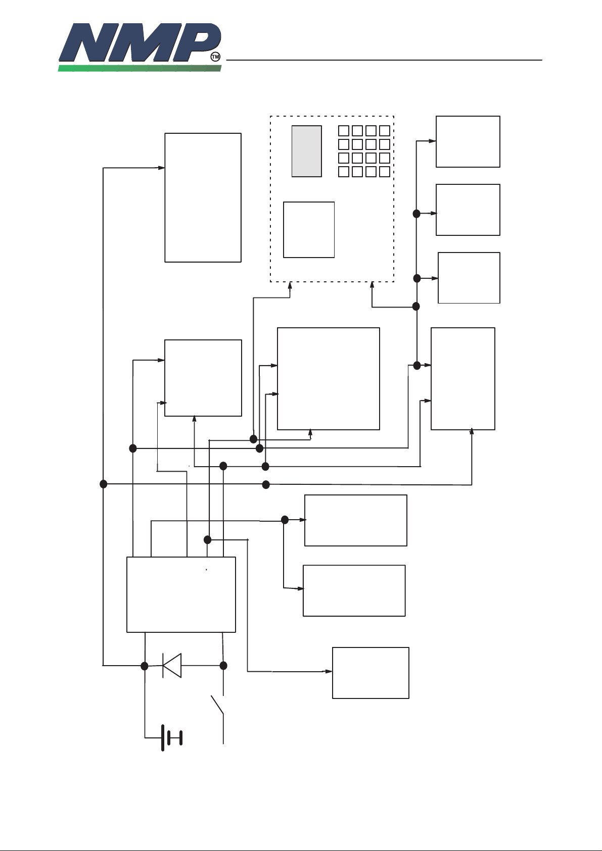
System Module GR4
Technical Summary
All functional blocks of the baseband are mounted on a single multi layer
printed circuit board. This board contains also RF–parts. The chassis of the ra-
dio unit contains separating walls for baseband and RF. All components of the
baseband are surface mountable. They are soldered using reflow. The connec-
tions to accessories are fed through the bottom connector of the radio unit. The
connections to User Interface –module (UIF) are fed through a flex foil connec-
tor. There is no physical connector between RF and baseband.
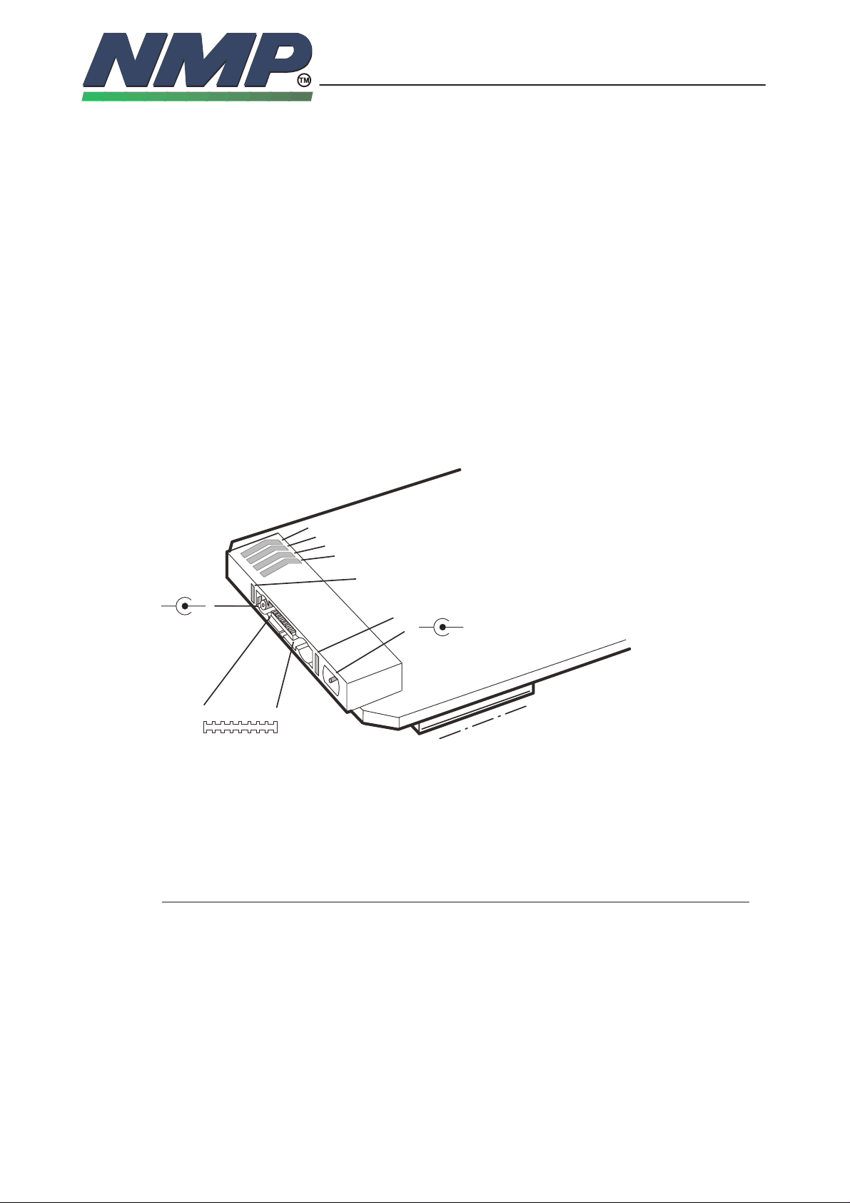
External and Internal Connectors
The system module has two connector, external bottom connector and internal
UIF module connector.
8–5
Copyright Nokia Mobile Phones
Antenna
connector
2
1
16
System connector
Bottom Connector X100
System Connector
Pin: Name: Description:
1, 9 LGND Digital ground. Separated with a choke from
4
Battery connector
3
2
1
4
Charging connector
X100
9
18
3
2
30
1
1
X196
UIF module connector
D0000323
PCB–gound
2 XMIC_JCONN External audio input from accessories or
handsfree microphone.
3 AGND Analog ground.
4 TDA DBUS transmitted data.
Page 6

SYSTEM MODULE GR4/GP4
NHC–4
11/97JR
Technical Documentation
Copyright Nokia Mobile Phones
8–6
5 M2BUS Serial bidirectional data and control between
the handportable and accessories.
6 HOOK/RXD2 HOOK indication. The phone has a 100 kΩ
pull–up resistor.
7 PHFS/TXD2 Handsfree device power on/off, data to flash
programming device.
8, 16 VCHAR Battery charging voltage.
10 XEAR_HFJPWR External audio output to accessories or
handsfree speaker.
11 DSYNC DBUS frame sync DBUSCLKEN
12 RDA DBUS received data
13 BENA Booster enable, TX–timing control (open drain,
TX–power is on when BENA is low)
14 VF Programming voltage for FLASH.
15 DCLK DBUS data clock. DBUSCLK
Battery Connector
Pin: Name: Description:
1 VBAT Battery voltage
2 BSI Battery size identification
3 BTEMP Battery temperature sense
4 GND Ground
Charging Connector
Pin: Name: Description:
1 VCHAR Battery charging voltage
2 GND Ground
3 VCHAR Battery charging voltage
4 GND Ground
Antenna Connector
Pin: Name: Description:
1 RF EXT External antenna signal
2 GND Ground
Page 7

SYSTEM MODULE GR4/GP4
NHC–4
UIF Module Connector X196
Pin: Name: Description:
1 VL1 Logic supply voltage 4.65 V
2,17,20 GND Ground
3,30 VBAT Battery voltage
4 KEYLIGHT Backlights on/off
5–11 UIF(0;6) Lines for keyboard write and LCD–
12 UIF7 LCD lights on/off
13–16 COL(0;3) Lines for keyboard read
18 MICP Microphone (positive node)
19 MICN Microphone (negative node)
20 EARP Earpiece (positive node)
11/97JR
Technical Documentation
controller control
8–7
Copyright Nokia Mobile Phones
21 EARN Earpiece (negative node)
23 VA2 Analog supply voltage 4.65 V
24 ONKEYX Power key (active low)
26 MIC_EN Microphone bias enable (open drain,
active low)
29 BUZZER Buzzer control
Page 8

SYSTEM MODULE GR4/GP4
NHC–4
Baseband Block
Baseband block is designed for a handportable phone, that operates in DAMPS
system. The purpose of the baseband module is to control the phone and process audio signals to and from RF. The module also controls the user interface.
List of Submodules
CTRLU Control Unit for the phone
PWRU Power supply
DSPU Digital Signal Processing block
AUDIO Audio coding
ASIC UDSA2 – asic
RFI RF – baseband interface
These blocks are only functional blocks and therefore have no type nor material
codes.
11/97JR
Technical Documentation
8–8
Copyright Nokia Mobile Phones
Modes of Operation
There are the following operating modes in the phone: Analog control channel,
Analog speech channel, Digital control channel, Digital traffic channel and out–
of–range.
Analog Control Channel Mode (ACC)
Radio unit is ready for reception on analog control channel. Most of the time
only RX–modem of UDSA2–asic and clock for it are operational. All other circuitry is powered down. Sometimes UDSA2 detects incoming data and wakes
up the MCU to read it. MCU determines whether the data is meant for that particular phone or not. If the call is detected, the phone moves to analog voice
channel or digital traffic channel mode depending on the orders by the base
station. Occasionally the phone communicates with the base station and then
the phone must be powered up.
Out of Range Mode (OOR)
All circuitry is powered down except a timer in UDSA2. After the timer has
elapsed the phone tries to establish the connection to base station. If it
succeeds, the phone goes to analog control channel mode. If the connection
can not be established the phone will stay in out of range mode, start the counter in ASIC and power down all other circuitry.
Page 9

SYSTEM MODULE GR4/GP4
NHC–4
11/97JR
Technical Documentation
Analog Voice Channel Mode (AVCH)
The phone is capable for analog receiving and transmitting. All circuitry is powered up except digital rx parts. MCU is in charge of the signalling between the
phone and the base station.
Whenever possible the circuits are put to sleep or standby.
Digital Control Channel Mode (DCC)
On digital control channel (DCC) DSPU receives the paging information from
the Paging channel (PCH) or Broadcasting channel (BCCH). DSPU sends messages to MCU for processing them.
Phone is in sleep between pagings.
From DCC phone may be commanded to analog control channel or to analog
or digital traffic channel
Digital Traffic Channel Mode
8–9
Copyright Nokia Mobile Phones
The phone is capable for receiving and transmitting on digital traffic channel. All
circuitry is powered up, except FM detector.
On digital trafic channel DSPU processes speech signal in 20 ms time slots.
DSPU performs the speech and channel functions in time shared fashion and
sleeps whenever possible. Rx and tx are powered on and off according to the
slot timing. MCU is waken up mainly by DSPU, when there is signalling information for the CS.
Supply voltages and power consumption
Line symbol Minimum Typ/nom Maximum Unit/notes
VBAT 5.3 V 6.0 V 9.0 V
VCHAR 11.0 V 13.0 V
VA1 4.5 V 4.65 V 4.8 V Imax = 40 mA
VA2 4.5 V 4.65 V 4.8 V Imax = 80 mA
VL1 4.5 V 4.65 V 4.8 V Imax = 150 mA
VL2 4.5 V 4.65 V 4.8 V Imax = 150 mA
VREF 4.6 V 4.65 V 4.8 V Imax = 5 mA
VF 11.4 V 12 V 12.6 V
Page 10

SYSTEM MODULE GR4/GP4
NHC–4
Audio Control Signals
The nominal values correspond ±2.9 kHz peak deviation.
Line symbol Minimum Typ./nom. Maximum
MICP, MICN 106.1 mV
EARP, EARN 43.7 V
EXTEAR
• min d.c. level 2.0 V 158 mV
XMIC
• min d.c. level 2.0 V 11 kΩ pull–down
resistor in HP 71 mV
Current Consumption
State VL1/mA VL2/mA VA1/mA VA2/mA
11/97JR
Technical Documentation
rms
8–10
Copyright Nokia Mobile Phones
rms
rms
rms
1.384 V
600 mV
1026 mV
rms
rms
rms
NOSERV 12 1.2 <50 µA <50 µA
SERV Ana 18 1 13 µA 140 µA
Analog call 43 50 8.4 11
Digital call 43 63 4.6 11
VL1 = MCU, SRAM, FLASH, ASIC, RFI, EEPROM, UI
VL2 = DSP1, DSP–rams
VA1 = RFI
VA2 = AUDIO codec, UI
Page 11
SYSTEM MODULE GR4/GP4
NHC–4
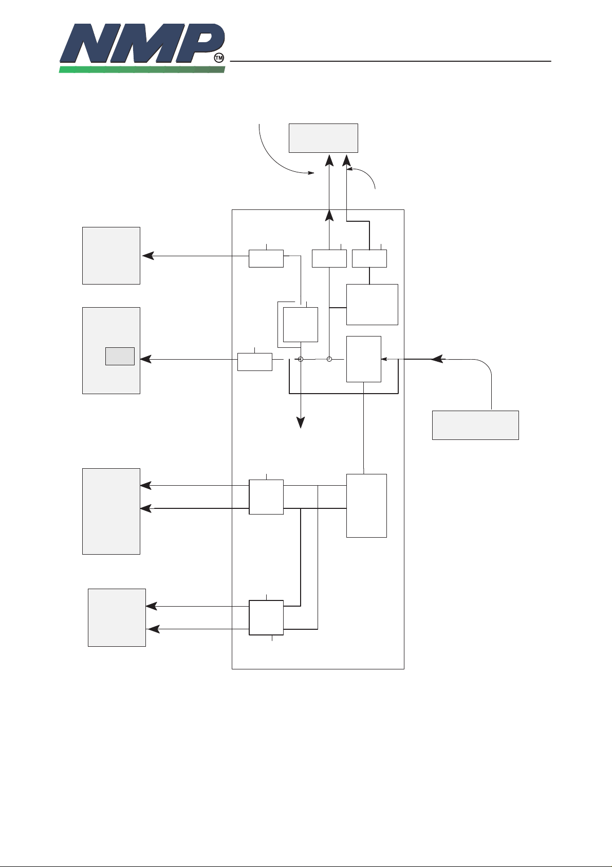
Clocking Schemes
MCU 1x clock: 4.86 / 9.72 MHz
MCU
DSP Clock: 9.72 MHz
DSP
38.88 MIPS
PLL
2x, 4x
11/97JR
Technical Documentation
RFI Clock: 9.72 MHz
MCU CCR bit 1
programmed
frequency
MCU CCR
bit 0
DIV2
DSP CCR
bit 2
EN
RFI2
ENEN
Copyright Nokia Mobile Phones
RF 2nd IF freq: 9.72 /4 = 2.43 MHz
RFI2 clock 106kHz
DSP
CCR
bit 3
DSP
CCR
bit 14
EN
DIV
91.7
DIV2
8–11
VCTCXO
ASIC System Clock
AUDIO
CODEC
DBUS
Data clock
512 kHz (d–mode)
518.4 kHz (a–mode)
8.0 kHz (d–mode)
8.1 kHz (a–mode)
Sync clock
Data clock
512 kHz
Sync clock
8.0/64 kHz
MCU CCR bit 2, DSP CCR bit 0
EN
DSP CCR
bit12
EN
DSP CCR bit 11
frequency
DIV
18.75
DIV
1200
RF System Clock:
19.44 low level
sine wave
UDSA2
UDSA2 uses an unbuffered clock from the VCTCXO. MCU can select its clock
frequency: 4.86 MHz, 9.72 or 19.44 MHz (default 9.72 MHz). DSP uses internal
4X PLL for generating the 38.88 MHz. Audio codec uses different clocks in A–
and D–mode. VCTCXO oscillator is running all the time.
All of the clock outputs can be disabled/enabled. DSP controls the DSP clock
and MCU clock is controlled by MCU. If DSP is in sleep mode, MCU can wake
Page 12
SYSTEM MODULE GR4/GP4
NHC–4
it up by sending a PIO–message. MCU and DSP clocks are also controlled by
the sleep clock.
Reset and Power Control
reset in
DSP
11/97JR
Technical Documentation
RFI
reset in
ASIC
RFI Reset Out
DSP Reset Out
MCU Reset Out
resetreg
Vcc
Reset in
resetreg
8–12
Copyright Nokia Mobile Phones
LCD
Reset in
PSL+
VL1
XRES reset in
XPWRON
XPwrOff
approx 0.5s
The supply power is switched on by PWR key on keyboard. All devices are
powered up at the same time by PSL+.
PSL+ supplies the reset to ASIC at power up. ASIC starts the clocks to DSP
and MCU. After 100 ms delay the PSL+ release the reset to ASIC, and ASIC
releases the resets to all circuitry. Power up reset resets MCU , RFI and DSP.
For powering of the phone, the user pushes PWR–key. MCU detects that it is
pushed. After that the MCU cuts the eventual ongoing call, exits all tasks, acts
dead to the user and leaves PSL+ watchdog without resets. After power–down
delay PSL+ cuts the supply voltage from all the circuitry.
XPWRON
MCU
Page 13

SYSTEM MODULE GR4/GP4
NHC–4
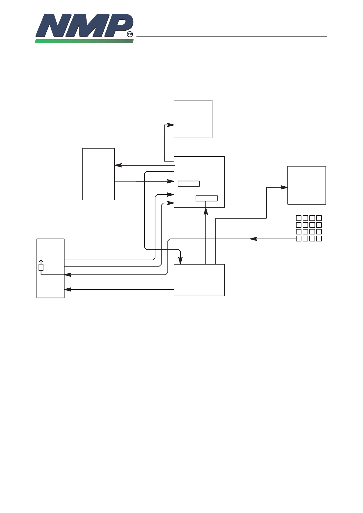
Watchdog System
PSL
11/97JR
Technical Documentation
reset
DSP
1
5
POWER
3
8–13
Copyright Nokia Mobile Phones
4
ASIC
4
2
reset
XPWROFF
Normal operation:
1 MCU tests DSP
2 MCU updates ASIC watchdog timer (> 2 Hz)
3 MCU pulses the XPWROFF input on the PSL+
Failed operation:
4 SIC resets MCU and DSPs (After about 0.5 sec failure)
5 PSL+ switches the power off (After 0.750 ms failure)
MCU
(about 2 Hz)
Page 14

SYSTEM MODULE GR4/GP4
NHC–4
CTRLU
Introduction
The Control block provides a mastercomputer unit (MCU) and it’s environment.
The environment consists of three memory circuits (FLASH, SRAM, EEPROM),
20 bit address bus and 8 bit data bus.EEPROM uses serial communication.
MCU functions:
– system control
– communication control
– user interface
– authentication
– RF monitoring
– power up/down control
– accessory monitoring
11/97JR
Technical Documentation
8–14
Copyright Nokia Mobile Phones
– battery monitoring
– self–test and production testing
– charging control
Input Signals of CTRLU
Signal name Signal description From
VL1 Power supply voltage for CTRLU block PWRU
VREF Reference voltage for MCU A/D converter PWRU
VBATDET Battery voltage detection PWRU
VC Charger voltage monitoring PWRU
ROMSELX Chip select for the FLASH memory ASIC
RAMSELX Chip select for the SRAM memory ASIC
RESETX Reset signal for MCU ASIC
NMI Non–maskable interrupt request ASIC
MCUCLK Main clock for MCU ASIC
IRQX Interrupt request ASIC
MBUSOUT Transmitted M2BUS–data from M2BUS– ASIC
circuitry of ASIC
PCMCDO Audio codec control data receiving AUDIO
RSSI Received signal level indicator RF
TRF RF module temperature detection RF
Page 15

SYSTEM MODULE GR4/GP4
NHC–4
TXF Transmitter on/off error control RF
VF Programming voltage for flash memory System conn.
JCONN Indicates if phone is connected to car System conn.
RXD2_HOOK The use of handsfree monitoring System conn.
BTEMP Battery temperature detection Battery conn.
BSI Battery size identification Battery conn.
Outputs Signals of CTRLU
Signal name Signal description To
11/97JR
Technical Documentation
Copyright Nokia Mobile Phones
installation bracket. When phone is
connected to car installation bracket, this
signal has about 2 V d.c. level, otherwise
d.c. level is 0 V.
Flash programming data input on the
production line
Vibrator battery control signal
8–15
XPWROFF Power off control, PSL+ watchdog reset PWRU
PWM Charger on/off control PWRU
MCUASX MCU address strobe ASIC
WSTROBEX MCU write strobe ASIC
RSTROBEX MCU read strobe ASIC
MCUAD(19;0) 20–bit MCU address bus ASIC
MBUSDET MBUS activity detection ASIC
TXD Transmitted M2BUS–data to M2BUS– ASIC
circuitry of ASIC.
PCMCLK Clock for audio codec control data AUDIO
transfer
PCMCDI Audio codec control data transmitting AUDIO
XSELPCMC Chip select for audio codec AUDIO
TXD2_PHFS Power on/off control for HF device System conn.
Verification output of the programmed
data of flash on the production line
UIF8 Call–led control Uif conn.
BUZZER Buzzer signal to earphone Uif conn.
Page 16

SYSTEM MODULE GR4/GP4
NHC–4
Bidirectional Signal of CTRLU
Signal name Signal description To/From
MCUDA(7;0) MCU’s 8 bit data bus ASIC,memories
M2BUS Asyncronous serial data bus System conn.
Block Description of CTRLU
MCU – Memories
MCU has a 20 bits wide address bus A(19:0) and an 8–bit data bus with memories. The address bits A(19:16) are used for chip select decoding. The decoding is done in UDSA2–asic.
On the Hitachi HD647534 internal memory map there is the following:
00000 – 07FFF 32k bytes internal ROM
0F680 – 0FE7F 2k bytes internal RAM
11/97JR
Technical Documentation
8–16
Copyright Nokia Mobile Phones
0FE80 – 0FFFF 384 bytes registers
External memory map is the following:
08000 – 0FFFF 32k bytes RAM
30000 – 300FF 256 bytes ASIC
80000 – BFFFF 256k bytes FlashROM
CTRLU – PWRU
MCU controls the watchdog timer in PSL+. It sends a positive pulse at approximately 2 Hz to XPWROFF pin of the PSL+ to keep the power on. If MCU fails to
deliver this pulse, the PSL+ will remove power from the system. MCU controls
also the charger on/off switching in the PWRU block. When power off is requested MCU leaves PSL+ watchdog without reset. After the watchdog has
elapsed PSL+ cuts off the supply voltages from the phone.
CTRLU – ASIC
MCU and ASIC have a common 8 bit data bus and a 9 bit address bus. A(5:0)
are used for normal addressing whereas bits A(19:16) are decoded in ASIC to
chip select inputs for CTRLU memories. ASIC controls the main clock, main reset and interrupts to MCU. The internal clock of MCU is half the MCUCLK clock
speed. RESETX resets everything in MCU except the contents of the RAM.
IRQX is general purpose interrupt request line from ASIC. After IRQX request
the interrupt register of asic is read to find out the reason for interrupt. NMI–interrupt is used only to wake up MCU from software standby mode.
CTRLU – DSPU
MCU and DSP communicate through ASIC. ASIC has MCU mailbox and DSP–
mailbox. MCU writes data to MCU mailbox where DSP can only read the incoming data. In DSP–mailbox data transfer direction is opposite.
Page 17

SYSTEM MODULE GR4/GP4
NHC–4
11/97JR
Technical Documentation
Copyright Nokia Mobile Phones
8–17
CTRLU – AUDIO
When the the chip select signal XSELPCMC goes low, MCU writes or reads
control data from AUDIO at the rate defined PCMCLK. PCMCDI is output data
line from MCU to codec and PCMCDO is input data line from codec to MCU.
CTRLU – BATTERY – Monitoring
MCU monitors battery functions with 3 channels (BTEMP, BSI,VBATDET) of an
8 channel A/D converter.
CTRLU – RF – Monitoring
MCU monitors RF functions with two channels (RSSI and TRF) of an 8 channel AD converter and one digital I/O–pin (TXI).
CTRLU – Keyboard and LCD Driver Interface
MCU and User Interface communication is controlled through ASIC.
CTRLU – ACCESSORIES
M2BUS is used to control external accessories. This interface can be used also
to factory testing and service and maintenance purposes.
Behaviour in Different Modes
Analog Control Channel Modes
While on analog control channel the MCU and the peripherals are in standby.
From time to time the MCU must poll the states of the control lines from the accessories.
The UDSA2 gives an interrupt to MCU if RX–modem detects data on channel.
The MCU then wakes up and starts controlling the receiving. If the data was not
for that phone the MCU will go to standby. Otherwise it will continue to control
the phone and start establishing the call.
Another alternative to wake up the processor is that the user pushes any button
on the keyboard. After that the asic will give an interrupt and the MCU starts to
control the phone.
Out–of–Range Mode
In out–of–range mode the MCU is in standby most of the time. During that time
the input clock is also stopped to save power. ASIC wakes up the MCU from
time to time to control the search for control channels and to reset the PSL+
watchdog. MCU use OOR signal to cut off the voltages from receiver to save
power in out of range mode.
Analog Voice Channel Mode
During analog voice channel operation the MCU is in charge of the operation of
the phone. The MCU is sleeping always when it is possible.
Page 18

SYSTEM MODULE GR4/GP4
NHC–4
Digital Traffic Channel Mode
During digital traffic channel operation the MCU is in charge of the operation of
the phone. The MCU is sleeping always when it is possible.
Digital Control Channel Mode
While on analog control channel MCU and the peripherals are in standby. From
time to time the MCU must poll the states of the control lines from the accessories.
DSPU perioidically wakes up to receive the paging information from PCH or
BCCH. DSPU wakes up the MCU if message is for the phone. MCU processes
the messages and controls the phone accordingly. If message was not for the
phone, then DSPU goes back to standby.
Another alternative to wake up the processor is that the user pushes any button
on the keyboard. After that the asic will give an interrupt and the MCU starts to
control the phone.
Main Components
11/97JR
Technical Documentation
8–18
Copyright Nokia Mobile Phones
• Hitachi H8/534
– H8/534 is a CMOS microcomputer unit (MCU) comprising a CPU core and
on–chip supporting modules with 16 bit architecture. The data bus to outside
world has 8 bits.
• 512k*8 bit FLASH memory
– 150 ns maximum read access time
– contains the main program code for the MCU; in the beginning the DSP pro-
gram code locates also in FLASH
• 32k*8bit SRAM memory
– 100 ns maximum read access time
• 8k*8bit EEPROM memory
– serial communication
– contains user defined information
Page 19

SYSTEM MODULE GR4/GP4
NHC–4
PWRU
The power block makes the supply voltages for the baseband and includes also
the charging electronics.
Input Signals of PWRU
Signal name Signal description From
XPWRON PWR on switch UIF
XPWROFF Power off control CTRLU
VBATT Battery voltage System conn.
PWM Charger on/off control CTRLU
VCHAR Charging voltage System conn.
Output Signals of PWRU
11/97JR
Technical Documentation
8–19
Copyright Nokia Mobile Phones
Signal name Signal description To
XRES Master reset ASIC
VL1 Logic supply voltage 1. Max 150 mA. CTRLU,ASIC,
VL2 Logic supply voltage 2. Max 150 mA. DSPU
VA1 Analog supply voltage 1. Max 40 mA. RFI
VA2 Analog supply voltage 2. Max 80 mA. AUDIO,UIF
VREF Reference voltage 4.65V ±2%. Max. 5mA. CTRLU,ASIC,
VBATDET Switched VBATT divided by 2 CTRLU
VC Attenuated VCHAR CTRLU
Block Description of PWRU
PSL+ has an internal watchdog, voltage detection and charger detection functions. The watchdog will cut the output voltages if it is not resetted once in
about 0.5 seconds. The voltage detector resets the phone if the battery voltage
falls below 4.5 V.
RFI,UIF
RF
The charging electronics is controlled by the MCU. When the charging voltage
is applied to the phone while the phone is powered up, the MCU detects it and
starts controlling the charging.
If the phone is in power–off, the PSL+ will detect the charging voltage and start
the phone. If the battery voltage is high enough the reset will be released and
the MCU will start controlling the charging. If the battery voltage is too low the
phone is in reset and charging control circuitry will pass the charging current to
Page 20

SYSTEM MODULE GR4/GP4
NHC–4
the battery. When the battery voltage has reached 4.5 V the reset will be removed and the MCU starts controlling the charging. This all is invisible to the
user.
Main Components of PWRU
• PSL+ asic
– Makes the voltages, has power switch, charger and battery detection and
watchdog.
• Transistor BCP69–25 and Schottky STPS340U
– The charging current is passed through these components.
• Transistor BCX51
– VL regulators of PSL+ external output transistors.
11/97JR
Technical Documentation
8–20
Copyright Nokia Mobile Phones
Page 21

SYSTEM MODULE GR4/GP4
NHC–4
DSPU
11/97JR
Technical Documentation
Copyright Nokia Mobile Phones
8–21
The DSPU (Digital Signal Processing Unit) block is in charge of the channel
and speech coding according to the IS–54B (2120 Plus) and IS–136 (2160)
specs. The block consists of a TMS320C541 DSP and slow external RAMs.
The DSP chip contains 28k word internal mask ROM and 4k word internal RAM
The main functions by two main modes of the DSPU block are as follows:
– control and general functions:
– main control of the DSP
– communication with MCU and data adapter module
– RF control
– analog mode speech processing functions:
– pre–emphasis, de–emphasis
– expansion, compression
– analog audio signal filtering
– acoustic echo cancellation (only when the handset is used)
– digital mode speech processing functions:
– VAD (Voice Activity Detection)
– full rateVSELP (Vector Sum Exited Linear Prediction) speech co-
ding
– acoustic echo cancellation (only when the standard HF is used)
– analog mode modem functions:
– ST (Signalling Tone) signal generation
– SAT (Supervisory Audio Tone) signal detection and regeneration
– WBD (Wide Band Data) sending
– digital mode modem functions:
– raised cosine filtering
– channel equalization
– interleaving
– convolutional coding and decoding
– MAHO (Mobile Assisted HandOff) measurements
– AFC (Automatic Frequency Control)
– symbol and frame synchronization
– AGC (Automatic Gain Control)
– DTX (Discontinuous Transmission) control
– CRC generation and checking
Page 22

SYSTEM MODULE GR4/GP4
NHC–4
Input Signal of DSPU
Signal name Signal description From
VL2 Logic supply voltage 2. Max 150 mA. PWRU
DSPCLK Master clock for DSP ASIC
DSPRSTX Reset for the DSP ASIC
PCMDATRCLK, Differential PCM–data receive clock ASIC
PCMDATRCLKX
PCMOUT Received audio in PCM–format AUDIO
INT0, INT1 Interrupts for DSP ASIC
PCMCO–SYCLKX PCM–data bit sync clock ASIC
Output signal of DSPU
Signal name Signal description To
11/97JR
Technical Documentation
8–22
Copyright Nokia Mobile Phones
PCMIN Transmitted audio in PCM–format AUDIO
IOX I/O enable. Indicates access to DSP ASIC
RWX Read/WriteX ASIC
DSPAD(17;0) Address bus and control signals ASIC
Bidirectional signal of DSPU
Signal name Signal description To/From
DSPDA(15;0) 16–bit data bus ASIC
Block Description of DSPU
DSP communicates with MCU trough a mailbox in the UDSA2 ASIC. DSP communicate with the PCM codec with the SIO1 serial bus. DSP controls RFI and
RF through UDSA2.
Analog transmit
Audio signal in analog mode is fed to the PCM codec, where it is routed, amplified and converted by internal A/D converter into 64 kb/s bitstream. The digitized speech is processed by the DSP audio modules into 48.6 k samples/s audio. The samples are sent to the RFI’s AGC D/A converters. AGC DAC –output
signal is fed to VHF syntheziser to give FM modulation. DSP must also perform
echo cancelling in HF mode.
address space.
Page 23

SYSTEM MODULE GR4/GP4
NHC–4
11/97JR
Technical Documentation
Copyright Nokia Mobile Phones
8–23
Analog receive
In analog receive the demodulated analog signal is first A/D converted in RFI at
48.6 k samples/s. The samples are directed trough UDSA2 to DSP. DSP performs audio processing and finally transfers the digital audio at 64 kb/s to the
PCM codec, where they are D/A converted. Resulting audio signal is routed
and amplified to the earpiece or external loudspeaker.
Digital transmit
In digital transmit mode DSP processes speech data in 20 ms slots. It performs
VSELP speech coding, CRC generation, convolutional coding and interleaving.
Finally it sends the symbols to the UDSA2 modulator. The UDSA2 modulator
performs the π/4 DQPSK modulation. UDSA2 controls the transmit timing and
at specified intervals sends the I/Q samples at 97.2 k samples/s to RFI for TXI/
Q D/A converters.
Digital receive
In digital receive mode the 2.43 MHz IF signal from RF unit is converted with
RFI/Q A/D converters at sample rate of 48.6 k samples/s. The timing is controlled by UDSA2. DSP performs bit detection with equalizer and then convolutional decoding and CRC checking. After this the (speech) bits are passed for
VSELP speech decoding. The decoded bits are converted to analog signal in
the PCM codec, routed and fed to the earpiece.
Analog modem functions
Analog modem decoding functions: ST and SAT. but not Wide Band Data
(WBD) are performed by the DSP. All modem transmit functions are performed
by DSP. WBD is received through an external BP filter and decoded (Manchester decoding, 3/5 vote and BCH decoding) by the UDSA2 modem. In XSTBY
mode, the 3/5 voting is not used.
Control functions
In all modes except analog control channel mode DSP controls the RF. Controlling is done physically through UDSA2, where all necessary timing functions
are implemented, and control I/O lines are provided for e.g. syntheziser loading, power control etc.
All clocks and timing are generated from the RFC clock, which is amplified in
the ASIC block.
Page 24

SYSTEM MODULE GR4/GP4
NHC–4
Modes of Operation
DSP goes to sleep by first executing clock stop command to UDSA2 and then
executing IDLE2 instruction. When DSP is in standby, the clock is disabled and
PLL also stopped. DSP is woken up from the sleep by UDSA2 by first starting
the clock and then after a delay issuing an interrupt0/1. No reset is needed.
Analog Control Channel (ACC)
DSP is used to CRC–status checking
Out of Range Mode (OOR)
DSP is used for searching for digital control channels in digital mode. MCU
searches for analog control channels.Synthezisers are controlled by DSP.
Analog Voice Channel Mode (AVCH)
On analog voice channel DSP performs the audio processing, FM modulation,
and signalling except WBD reception. In the HF mode it also performs echocancellation and the HF algorithm.
Digital Traffic Channel Mode (DTCH)
11/97JR
Technical Documentation
8–24
Copyright Nokia Mobile Phones
DSP processes the speech signal in 20 ms slots. RX, TX and MAHO are timed
by the UDSA2 timers. DSP sleeps whenever possible.
Main Components of DSPU
• TI TMS320C541 DSP
– 38.88 MIPS
– 4k RAM/ 28k ROM
– 2 SIOs, 1 timer
– programmable PLL for clocking (4X used: 4*9.72MHz = 38.88MHz)
– 2*32 kb 70 ns external RAM
Page 25

SYSTEM MODULE GR4/GP4
NHC–4
AUDIO
The block consists of audio codec with some peripheral components. The codec includes microphone and earpiece amplifier and all the necessary switches
for routing. The controlling of the codec is done by the MCU. The PCM data
comes from and goes to DSPs.
Input signal of AUDIO
Signal name Signal description From
VA2 Analog supply voltage 1. Max 80 mA. PWRU
PCMIN Received audio in PCM–format DSPU
SYNC 8kHz/8.1kHz frame sync ASIC
CODEC_CLK 512kHz/518.4kHz codec main clock ASIC
11/97JR
Technical Documentation
(=PCMCOSYCLK)
(=PCMDATRCLK)
8–25
Copyright Nokia Mobile Phones
PCMCDI Audio codec control data CTRLU
PCMCLK Clock for audio codec control data CTRLU
XSELPCMC Audio codec chip select CTRLU
XMIC–JCONN External microphone System conn.
MICN,MICP Differential microphone signal UIF conn.
Output signal of AUDIO
Signal name Signal description To
PCMOUT Transmitted audio in PCM–format DSPU
PCMCDO Audio codec control data CTRLU
MIC_EN Microphone enable UIF
XEAR_HFJPWR External received audio System conn.
JCONN XMIC_JCONN connection signal level ASIC
EARN,EARP Internal received audio UIF
transfer
indicator
BUZZ Vibrator control signal Vibrators
Page 26

SYSTEM MODULE GR4/GP4
NHC–4
Block Description of AUDIO
The audio codec communicates with the DSP through a SIO (signals: PCMIN,
SYNC, CODEC_CLK and PCMOUT) . MCU controls the audio codec functionality through a separate SIO (signals: PCMCDO, PCMCDI, PCMCLK and
XSELPCMC).
Analog control channel
The codec is in standby except when keybeeps are needed. LO output is floating in standby and it disables the microphone bias circuit on flex.
Analog out of range mode
The codec is in standby and microphone bias current is removed.
Analog voice channel mode
The PCM–data is connected to the DSP.
Digital mode
The PCM–data is connected to the DSP.
11/97JR
Technical Documentation
8–26
Copyright Nokia Mobile Phones
Main Componets of AUDIO
• Audio codec ST5090
– Includes e.g. PCM codec, audio routing switches, microphone and earpiece
amplifiers for 2 connections (internal and external devices) and DTMF generator. Buzzer control is used for vibrator control.
Page 27

SYSTEM MODULE GR4/GP4
NHC–4
ASIC
11/97JR
Technical Documentation
Copyright Nokia Mobile Phones
This block mainly consists of DAMPS specific asic (UDSA2). It also includes
RX modem filter and RFC clock buffer. The ASIC takes care of the following
functions:
– interface between MCU and UIF
– interface between DSP and MCU
– interface between MCU, DSP and RFI
– clock generation and disable/enable
– RX signalling message receiving for analog control and voice channels
– RF–controls
– UIF–interface
– Timers
– M2BUS interface
8–27
Input Signals of ASIC
Signal name Signal description From
VL1 Logic supply voltage 1. Max 150 mA PWRU
VREF Reference voltage PWRU
ADATA/92 Receiver IF/analog received signal to RF
IOX/129 I/O enable, indicates access to DSP DSPU
RWX/130 Read/writeX DSPU
WSTROBEX/55 MCU’s write strobe CTRLU
RSTROBEX/56 MCU’s read strobe CTRLU
RFC/2 Ref. clock from VCTCXO (19.44 MHz) RF
PORX/88 Master reset PWRU
DSPAD(17:0) Address bus and control signals DSPU
MCUAD(19:0) MCU’s 20 bit address bus CTRLU
analog modem
address space
TXD/79 Transmitted M2BUS data to M2BUS CTRLU
circuitry of ASIC
MCUASX/74 MCU’s address strobe CTRLU
DAX/15 Data acknowledge RFI
MBUSDET/58 MBUS activity detection CTRLU
Page 28

SYSTEM MODULE GR4/GP4
NHC–4
Output signals of ASIC
Signal name Signal description From
INT0X/117 Interrupts for DSP DSPU
INT1X/116
NMI/68 Not maskable interrupt request CTRLU
IRQX/69 Interrupt request CTRLU
SYSRESETX/14 Master (power up) reset CTRLU
DSPRSTX/121 Reset for the DSP DSPU
WRX/16 Write strobe RFI
RDX/17 Read strobe RFI
RFIAD(3:0) RFI address bus RFI
SCLK/5 Synte load clock RF
SDATA/6 Synte load data RF
11/97JR
Technical Documentation
8–28
Copyright Nokia Mobile Phones
SENA1/7 Receiver synte enable RF
SENA2/4 Fast synte enable RF
TXPWR/9 TX circuitry power enable RF
SYNTHPWR2/10 Synte circuitry power enable RF
TXP/11 Transmit enable RF
TXLX/8 TX power level RF
TXA/12 RF power control loop adjustment RF
RXPWR/119 Receiver power control RF
BOOTSELX/137 RX_UHF_LO buffer current control RF
(used to TXPWR2 purpose)
BENA/89 Booster enable System conn.
MCUCLK/70 Main clock for MCU CTRLU
RFICLK/35 RFI master clock RFI
RFI2CLK/34 RFI sleep clock RFI
PCMDATRCLK/94 Differential PCM data receive clock DSPU, AUDIO
PCMDATRCLKX/115Differential PCM data receive clock, inver. DSPU
PCMCOSYCLK/95 Differential bit sync clock AUDIO
PCMCOSYCLKX Differential bit sync clock, inverted DSPU
/118
MBUSOUT/91 MBUS output from MBUS logic CTRLU
ROMSELX/81 Chip select for the FLASH memory CTRLU
Page 29

SYSTEM MODULE GR4/GP4
NHC–4
EROMSELX/80 Chip select for the EEPROM memory (nc) CTRLU
RAMSELX/82 Chip select for the SRAM memory CTRLU
COL(3:0)/107–104 Lines for keyboard column write UIF
KEYLIGHT/113 Keyboard backlight on/off control UIF
UIF7/114 LCD display backlight on/off control UIF
REF_CONTROL RFI reference voltage control RFI
RXTX10/140 RFI reset control RFI
Bidirectional signals of ASIC
Signal name Signal description From
DSPDA(15:0)/54–39 16 bit data bus DSPU
MCUDA(7:0)/60–67 MCU’s 8 bit data bus CTRLU
RFIDA(11:0)/22–33 12 bit data bus RFI
11/97JR
Technical Documentation
8–29
Copyright Nokia Mobile Phones
UIF(6:0)/97–103 LCD controller control and keyboard UIF
Block Description of ASIC
RFC buffer buffers the 19.44MHz clock from VCTCXO to ASIC. In ASIC that
clock is further buffered and divided for MCU, RFI, DSP (9.72MHz) and audio
codec (main and sync clocks). The clock outputs can be disabled in order to
save current when the clock is not needed.
The filtering of DAF signal from RF receiver is done using a second order BP
filter. After filtering it is squared to logic levels for ASIC.
Main Components of ASIC
• UDSA2 asic
• passive filtering and opamp for DAF squaring
read bus
Page 30

SYSTEM MODULE GR4/GP4
NHC–4
RFI
11/97JR
Technical Documentation
Copyright Nokia Mobile Phones
8–30
The block consists of RFI–ASIC and its reference voltage generator. This block
is an interface between RF and baseband. The block has the following functions:
– IF receiving and A/D conversion
– I/Q separation
– I and Q transmit and D/A conversion
– AFC D/A
– TXC, also used as an analog AGC
– AGC DAC, is used to provide FM modulation
– Analog signal for analog transmit an receive, power level and mixer bias
The RFI is connected to DSA with a 12 bit databus. The registers in RFI are ac-
cessed using 4 address bits.
Inputs signals of RFI
Signal name Signal description From
VL/48,52,60 Logic supply voltage 1. Max 150 mA. PWRU
VA2/2,5,10,13 Analog supply voltage 2. Max 80 mA. PWRU
VREF Referens voltage from PSL+ (4.65V) PWRU
RFIRESETX/18 RFI reset ASIC
RFIAD(3;0)/31–34 RFI address bus ASIC
RDX/49 Read strobe ASIC
WRX/50 Write strobe ASIC
RFICLK/53 RFI master clock ASIC
RFI2CLK/59 RFI sleep clock ASIC
RXQ,RXI/1,63 Receiver IF/analog received signal RF
AFC_CONTROL AFC line float/middle of the range control MCU
REF_CONTROL Reference voltage/VB_ext on/off control ASIC
Page 31

SYSTEM MODULE GR4/GP4
NHC–4
Output signals of RFI
Signal name Signal description To
DAX/51 Data acknowledge ASIC
AFC/14 Automatic frequency control voltage RF
PDATA0/29 AGC control RF
AMOD/16 analog baseband transmit signal RF
TXC/6 TX transmit power control voltage RF
TXQP/8,TXQN/9 differential TX quadrature signal RF
TXIP/11,TXIN/12 differential TX inphase signal RF
MODE/19 Analog/digital mode control RF
Bidirectional of RFI
Signal name Signal description To/From
11/97JR
Technical Documentation
8–31
Copyright Nokia Mobile Phones
RFIDA(11;0)/35–40, 12 bit data bus ASIC
42–47
Main Components of RFI
• RFI asic
• 4.096 V external voltage reference LM4040 for RFI
Page 32

SYSTEM MODULE GR4/GP4
NHC–4
11/97JR
Technical Documentation
RF Module Block
RF block is designed for a hand portable phone, which operates in AMPS and
DMR systems. Purpose of the RF module is to receive and demodulate radio
frequency signal from the base station and to transmit a modulated RF signal to
the base station. RF parts are designed for power class IV. Power class can be
increased to class I with external booster amplifier.
List of Functional Blocks
• RX, Receiver
• TX, Transmitter and modulator
• SYNT, UHF and VHF synthesizers
Constructions and Connections
All functional blocks of the RF are mounted on single multilayer printed circuit
board. This board contains also MCU and DSP functions. Chassis of the radio
unit contains separating walls for RF subblocks and DSP. All components of
the RF are SMD type, which are soldered using reflow solder. Signals to booster amplifier are fed via bottom connector of the radio unit.
8–32
Copyright Nokia Mobile Phones
RF Frequency Plan
44.545 MHz
869–894 MHz
LO 1
914–
939 MHz
824–849 MHz
455 kHz
1st IF 2nd IF
45 MHz 2.43 MHz
47.43 MHz
f
f/2
90 MHz
f/2
PLL
f
Analog mode output
CRFRT
f
f/2
Digital mode output
D–mode:
RX: 189.72 MHz
LO 2
TX: 180 MHz
A–mode:
180 MHz
VCTCXO:
19.44 MHz
Page 33

SYSTEM MODULE GR4/GP4
NHC–4
Functional Description
Receiver
The receiver is a double conversion receiver.
The received RF signal from the antenna is fed via a duplex filter to the receiv-
er unit. The signal is amplified by a discrete low noise preamplifier. In digital
mode the gain of the amplifier is controlled by the AGC control line (PDATA0).
The nominal gain of 10 – 15 dB is reduced in the strong field condition about
25 – 30 dB. After the preamplifier the signal is filtered by SAW RF filter. The
filter rejects spurious signals coming from the antenna and spurious emissions coming from the receiver unit.
The filtered RF– signal is down converted by a passive diode mixer. The frequency of the first IF is 45 MHz. The first local signal is generated by the UHF
synthesizer. The IF signal is amplified and then it is filtered by crystal filter. The
filter rejects adjacent channel signal, intermodulating signals and the second IF
image signal. The filtered 1st IF is amplified and fed to the receiver part of the
integrated RF circuit CRFRT in digital mode and to FM IF IC in analog mode.
11/97JR
Technical Documentation
8–33
Copyright Nokia Mobile Phones
In CRFRT the IF signal is amplified by an AGC amplifier which has gain control
range of 57 dB. The gain is controlled by an analog signal via TXC–line.
The amplified IF signal is down converted to the second IF in the mixer of
CRFRT. The second local signal is generated from VHF VCO by dividing the
original signal by 4 in the dividers of CRFRT.
The second IF frequency is 2.43 MHz. The second IF is filtered by a ceramic
resonator filter.The filter rejects signals of the adjacent channels. The filtered
second IF is fed back to CRFRT where it is amplified and fed out to RFI via
RXI and RXQ lines.
In analog mode the filtered and amplified first IF signal is fed to the FM IF IC
circuit. In this IC the signal is down converted to the second IF 455 kHz. Limitting amplifiers and detector operate on this frequency. Demodulated signal is
fed to RFI via RXI–line. Demodulated wideband data is fed to system asic. FM
IC produces also RSSI voltage which is propotional to the received RF signal
strenght. Injection for 2nd mixer is generated in crystal oscillator circuit (44.545
MHz).
Frequency Synthesizers
The stable frequency source for the synthesizers and base band circuits is voltage controlled, temperature compensated crystal oscillator, VCTCXO module.
The frequency of the oscillator is 19.44 MHz. It is controlled by an AFC voltage,
which is generated by the base band circuits. In digital mode receiver is locked
to base station frequency by AFC. In analog mode AFC voltage is fixed (there
is no automatic frequency control).
Page 34

SYSTEM MODULE GR4/GP4
NHC–4
The UHF synthesizer generates the down conversion signal for the receiver
and the up conversion signal for the transmitter. UHF frequency is 914.04 ...
938.97 MHz, depending on the channel which is used.The UHF VCO is a module. The PLL circuit is dual PLL, common for both UHF and VHF synthesizers.
The VHF synthesizer signal ( divided by 4 in CRFRT) is used in digital RX
mode as a local for the second mixer. Also the VHF signal (divided by 2 in
CRFRT) is used in the I/Q modulator of the transmitter.
In analog mode VHF synthesizer signal is only used for transmitter. Analog
modulation is generated in VHF synthesizer.
In digital mode VHF synthesizer frequency is 180.0 MHz during transmitting
and 189.72 MHz during receiving. In analog mode VHF frequency is 180.0
MHz.
Transmitter
The TX intermediate frequency is modulated in digital mode by an I/Q modulator contained on transmitter section of CRFRT IC. The TX I and Q signals are
generated in the RFI interface circuit and they are fed differentially to the modulator. In analog mode modulation is fed to VHF synthesizer from AGC DAC in
RFI circuit.
11/97JR
Technical Documentation
8–34
Copyright Nokia Mobile Phones
Modulated intermediate signal is amplified or attenuated in temperature compensated controlled gain amplifier (TCGA). The output of the TCGA is amplified
and the output level of CRFRT is typically –10dBm.
The output signal from CRFRT is low–pass filtered to reduce harmonics and
noise. The final TX signal is achieved by mixing the UHF VCO signal and the
modulated TX intermediate signal with passive mixer. After mixing the TX signal is amplified and filtered by two amplifiers and two filters. The filters are microstripe filter and SAW–filter. After these stages the level of the signal is typically 1 mW (at highest power level).
The discrete power amplifier amplifies the TX signal to the desired power level.
Amplified TX signal is filtered in duplex filter. Then signal is fed via semirigid
cable to the antenna switch in the bottom connector. From the antenna switch
signal is fed to external antenna connector or via semirigid cable to the antenna. The maximum output level is typically 480 mW.
The power control loop controls the output level of the power amplifier. The
power detector consists of a directional coupler and a diode rectifier. Transmitted power is controlled with controlled gain amplifier (TCGA) on TX–path of
CRFRT. Power is controlled with TXC and TXP signals. The power control signal (TXC), comes from the RF interface circuit, RFI.
Page 35

SYSTEM MODULE GR4/GP4
NHC–4
11/97JR
Technical Documentation
Modes of Operation
Analog control channel mode
Radio unit ready for analog reception. UHF–synthesizer and RX analog parts
running, otherwise RF circuits powered down.
Analog out of range mode and extended stby mode
All RF circuits powered down except the reference frequency oscillator.
Analog voice channel mode
Analog receiver section running, UHF–synthesizer, VHF–synthesizer, modulator and transmitter power amplifier are activated. Digital part of the receiver
powered down.
Digital traffic channel mode
8–35
Copyright Nokia Mobile Phones
Digital receiver, UHF and VHF synthesizers, modulator and TX power amplifier
running, pulsed operation. Analog FM IF–circuit powered down.
Software Compensations
Power Levels (TXC) vs. Temperature
Because of wide temperature range and poor cooling of the RF block, it is necessary to compensate the effect of temperature on output power. To monitor
this environment change, temperature measurement is used. There is a table
of factor, which are used for temperature compensation, common values for all
power levels and both modes. The values for these are defined without factory
measurements. Temperature is measured and right compensation value is addad to TXC–value. Requirement for compensation update is for every 1 minutes
or after every 5 degrees C of temperature change. This means, that during
analog mode transmission there will be need for temperature reading and TXC
compensation update. Because of poor cooling of RF block and insufficient linearity in high temperatures, output power is reduced from level 2 to level 2.5
when temperature inside the phone is above +80 C in analog mode and above
+65 C in digital mode.
Power Levels (TXC) vs. channel
Duplexer frequency response ripple is compensated by software. Power levels
are calibrated on four channels in production. Values for channels between
these tuned channels are calculated using linear interpolation.
Page 36

SYSTEM MODULE GR4/GP4
NHC–4
11/97JR
Technical Documentation
Power Levels vs. Battery Voltage
For saving battery capacity and because of insufficient linearity in digital mode,
output power is decreased from level 2 to level 2.5, when battery voltage drops
below 5.6V.
Power Up/Down ramps
Transmitter output power up/down ramps are controlled by sw. A special ramp
tables are used for that. Requirement is for six different ramps. Separate ramps
are used in power up and power down ramps.
Digital Mode RSSI
Digital mode RSSI vs. input signal is calibrated in production, but RSSI vs. temperature and RSSI vs. channel are compensated by software.
RF Characteristics
8–36
Copyright Nokia Mobile Phones
Receiver
Duplex Filter
The duplex filter consists of two functional parts; RX and TX filters. The TX filter rejects the noise power at the RX frequency band and TX harmonic signals.
The RX filter rejects blocking and spurious signals coming from the antenna.
Pre–amplifier
The bipolar pre–amplifier amplifies the received signal coming from the antenna. In digital mode, in the strong field conditions the gain of the amplifier is reduced 28 dB, typically.
RX Interstage Filter
The RX interstage filter is SAW filter. The filter rejects spurious and blocking
signals coming from the antenna. It also rejects the local oscillator signal leakage to the antenna.
First mixer
The first mixer is a single balanced passive diode mixer. The local signal is balanced by a printed circuit transformer. The mixer down converts the received
RF signal to IF signal.
First IF amplifier
The first IF amplifier is a bipolar transistor amplifier.
Page 37

SYSTEM MODULE GR4/GP4
NHC–4
11/97JR
Technical Documentation
First IF filter
The first IF filter is a four pole crystal filter. The IF filter is for channal selectivity.
2nd first IF amplifier
The 2nd first IF amplifier is used to guarantee proper impedance matching to
the first IF filter output in both operating modes.
Receiver IF circuit, RX part of CRFRT (digital mode)
The receiver part of CRFRT consists of an AGC amplifier of 57 dB gain, a mixer
and a buffer amplifier for the last IF. The mixer of the circuit down converts the
received signal to the last IF frequency. After external filtering the signal is amplified and fed to baseband circuitry.
Second IF filter
The second IF filter is a ceramic filter, which makes part of the channel selectivity of the receiver. In digital mode second IF filter it is made using ceramic resonators.
8–37
Copyright Nokia Mobile Phones
FM IF circuit (analog mode)
The FM IF circuit is used in anlog mode. The IC is Toshiba TA31136FN including 2nd mixer, local oscillator, limiting if stages, quadrature detector and RSSI
function.
Transmitter
Modulator Circuit, TX part of CRFRT
The modulator is a quadrature modulator contained in Tx–section of CRFRT
IC. The I– and Q– inputs generated by RFI interface are DC–coupled and fed
via buffers to the modulator. The local signal is divided by two to get accurate
90 degrees phase shifted signals to the I/Q mixers. After mixing the signals are
combined and amplified with temperature compensated controlled gain amplifier (TCGA). Gain is controlled with power control signal (TXC). The output of the
TCGA is amplified and the maximum output level is –10 dBm, typically.
Unconversion mixer
The upconversion mixer is a single balanced passive diode mixer. The local
signal is balanced by a printed circuit transformer. The mixer upconverts the
modulated IF signal coming from quadrature modulator to RF signal.
Page 38

SYSTEM MODULE GR4/GP4
NHC–4
TX buffers
The TX buffers are a bipolar transistor amplifier. They amplifies the TX signal
coming from the upconversion mixer.
TX interstage filter
The TX filter rejects the spurious signals generated in the upconversion mixer.
It rejects also the local, image and IF signal leakage and RX band noise.
Power amplifier
The power amplifier is a two stage discrete amplifier using GaAs FETs CLY5
and CLY10. It amplifies the 0 dBm TX signal to the desired output level. It ihas
been specified for 6 volts operation. Power transistor bias is tuned in production
using the DAC in PLL circuit UMA1018.
Power control circuitry
11/97JR
Technical Documentation
8–38
Copyright Nokia Mobile Phones
The power control loop consists of a power detector and a differential control
circuit. The power detector is a combination of a directional coupler and a
diode rectifier. The differential control circuit compares the detected voltage
and the control voltage (TXC) and controls voltage controlled amplifier (in
CRFRT). The control circuit is a part of CRFRT.
Synthesizers
Reference oscillator
The VCTCXO signal is used for a reference frequency of the synthesizers and
the clock frequency for the base band circuits.
YHF synthesizer
The VHF synthesizer consists of the VHF VCO, PLL integrated circuit and loop
filter. The output signal is used for the 2nd mixer of the receiver in digital mode
and for the I/Q modulator of the transmitter. In digital mode the VCO changes
the frequency according to the RX/TX slot. In analog mode FM modulation is
done in VHF synthesizer. Bilateral switch is used to change operation mode;
slow analog mode or fast digital mode.
The VHF VCO uses a bipolar transistor as a active element and a combination
of a chip coil and varactor diode as a resonance circuit. The buffer is combined
into the VCO circuit so, that they use same collector current.
Page 39

SYSTEM MODULE GR4/GP4
NHC–4
UHF synthesizer
The UHF synthesizer consists of a UHF VCO, power divider, PLL circuit and a
loop filter. The output signal is used for the 1st mixer of the receiver and the
upconversion mixer of the transmitter.
UHF buffers
The buffers amplifies the UHF VCO signal. The output signal of UHF VCO is
divided into the 1st mixer of the receiver and the upconversion mixer of the
transmitter. There is one buffer for TX and one for RX.
PLL circuit
The PLL circuit is PHILIPS UMA1018. The circuit is a dual frequency synthesizer including both the UHF and VHF synthesizers.
11/97JR
Technical Documentation
8–39
Copyright Nokia Mobile Phones
Page 40
SYSTEM MODULE GR4/GP4
NHC–4
11/97JR
Technical Documentation
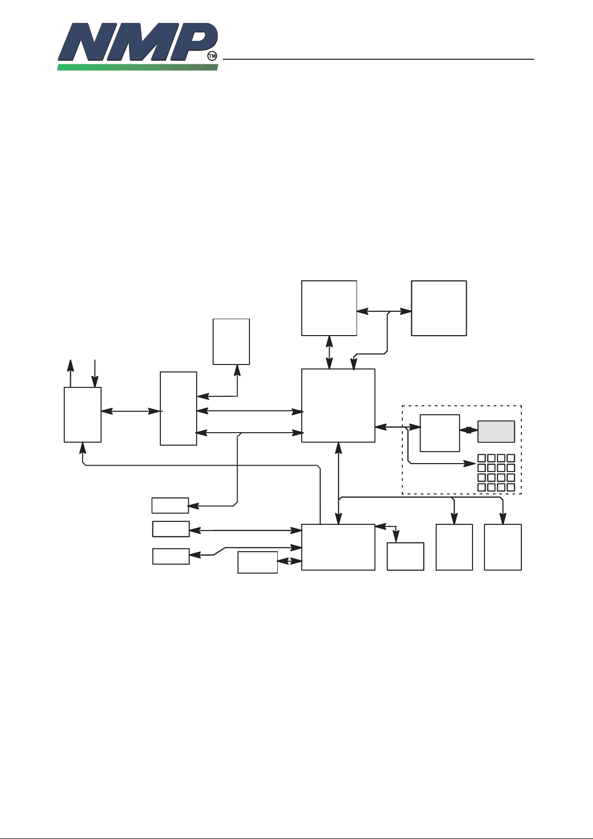
Baseband Block Diagram
ear–
piece
micro–
phone
32K x
16
SRAM
Copyright Nokia Mobile Phones
RFI RF
12 bit
12 bit
parallel + 8
parallel + 8
x control
x control
8–40
AUDIO
CODEC
SIO1
DBUS
PSL+
CHRG
R
FLASH
LOAD
DSP
MEM
space
I/O
space
SIO2
A15:0
D15:0
DBUSCLK
DBUSCLKEN
M2 Interface
A5:0,
A5:0,
D15:0
D15:0
io io ext mem
sio
sio
sio
UDSA2
A4:0
A19:16
D7:0
A19:0
D7:0
MCU
Serial
ExIIC
E2PROM
8K x 8
UIF–module
UIF–module
LCD driver
512K*8
FLASH
A17:0
D7:0
LCD
LCD
32K x 8
SRAM
A14:0
D7:0
Page 41

SYSTEM MODULE GR4/GP4
NHC–4
RF Block Diagram
RSSI
MODEM_DATA
455kHz
DEMOD
RXI
2.43MHz
11/97JR
Technical Documentation
RXQ
CONTROL
TX POWER
f/4
f
TXC
TXF
AFC
8–41
Copyright Nokia Mobile Phones
TXIP
TXIN
f/2
f
f/2
f
TXQP
TXQN
AMOD
PDATA5
VB_ext
TXA
CRFRT
44.545MHz
RF–BLOCK
ANA RX
45MHz
869...894MHz
PDATA0
DIGI RX
VHF
UHF
PLL
VCO
VCO
A:180MHz
D:189.72 / 180 MHz
914...939MHz
19.44MHz
VCTCXO
PLL
D/A
BIAS
90MHz
824...849MHz
FAST
SCLK
SENA1
RFC
TRF
T
TXPWR2
VBATT_TX
EXT.
ANT.
824...849MHz
+6 V
CRFCONT
+4.5V
TXP
DNEGA SDATA
TXPWR
MODE
TXLX
TXPWR2
RXPWR
SYNTEPWR1
SYNTEPWR2
VREF
VBATT
Page 42

SYSTEM MODULE GR4/GP4
NHC–4
11/97JR
Technical Documentation
Copyright Nokia Mobile Phones
RF Block Interconnection Diagram (GP4) (Version 5.63 ; edit 120)
8–42
Page 43
SYSTEM MODULE GR4/GP4
NHC–4
11/97JR
Technical Documentation
Baseband Power Distribution Diagram
LCD
LCD
VBAT
RF
LCD Driver
UIF–module
UIF–module
VA2
Copyright Nokia Mobile Phones
32K x 8
SRAM
VL1
128K x 8
FLASH
VL1
E2PROM
8K x 8
VL1
VL1
8–43
VL1
PSL+
VL2
VA1 VL1
VL3
VREF
VA1
RFI
VA2
VREF
ASIC
ASIC MCU
VREF VL1
VA2
DSP
VL2
DSP
VL2
ram
PCM
CODEC
VA2
MCU
VREF VL1
VBAT
VBAT
VCHAR
Page 44

SYSTEM MODULE GR4/GP4
NHC–4
11/97JR
Technical Documentation
RF Power Disribution Diagram
RF
Vbat
CRFCONT
MODE
&
VR7CNT
VR7
BASEVR8
Vbat
Copyright Nokia Mobile Phones
TX
TXPWR2
VTX_D:
CRFRT (VTXD)
VTX:
CRFRT (VTX)
TXbfrs
TXLbias
DNEGA
90 mA
8–44
Vbat
&
10 mA
PA
500mA
DNEGA
TXPWR
TXPWR2
SYNTHPWR1
SYNTHPWR2
VREF
RXPWR
MODE
VR8CNT
VR3CNT
VR4CNT
VR5CNT
CNTBIAS
VR1CNT
VR2CNT
&
VR6CNT
VR8
VR3
VR4
VR5
VBIAS
VR1
VR2
VR6
MODE
VULO:
UHF VCO
VHLO:
VHF VCO
VHF bfrs
CRFRT (VTX_slow)
9 mA
VFM:
FM–IC
4mA
VRX_D:
CRFRT(VRX)
35 mA
7 mA
VTX2:
UHF TX bfr
VRX_A:
LNA
1.IF bfrs
UHF RX bfr
17mA
10 mA
SYNTH
VXAO:
VCTCXO
PLL
CRFRT
(V_prot)
9 mA
RX
VB_ext
CRFRT
(VB_ext)
<1mA
Page 45

SYSTEM MODULE GR4/GP4
NHC–4
11/97JR
Technical Documentation
Copyright Nokia Mobile Phones
Parts List of GR4 EDMS Issue: 6.7 Code: 0200674
ITEM CODE DESCRIPTION VALUE TYPE
R001 1430804 Chip resistor 100 k 5 % 0.063 W 0402
R002 1430726 Chip resistor 100 5 % 0.063 W 0402
R003 1430726 Chip resistor 100 5 % 0.063 W 0402
R004 1430726 Chip resistor 100 5 % 0.063 W 0402
R005 1430726 Chip resistor 100 5 % 0.063 W 0402
R100 1430842 Chip resistor 680 k 1 % 0.063 W 0402
R101 1430840 Chip resistor 220 k 1 % 0.063 W 0402
R102 1430804 Chip resistor 100 k 5 % 0.063 W 0402
R103 1430804 Chip resistor 100 k 5 % 0.063 W 0402
R104 1430804 Chip resistor 100 k 5 % 0.063 W 0402
R106 1430770 Chip resistor 4.7 k 5 % 0.063 W 0402
R107 1430770 Chip resistor 4.7 k 5 % 0.063 W 0402
R108 1430764 Chip resistor 3.3 k 5 % 0.063 W 0402
R109 1430788 Chip resistor 22 k 5 % 0.063 W 0402
R110 1430754 Chip resistor 1.0 k 5 % 0.063 W 0402
R111 1430754 Chip resistor 1.0 k 5 % 0.063 W 0402
R112 1430770 Chip resistor 4.7 k 5 % 0.063 W 0402
R114 1430762 Chip resistor 2.2 k 5 % 0.063 W 0402
R115 1430788 Chip resistor 22 k 5 % 0.063 W 0402
R116 1430788 Chip resistor 22 k 5 % 0.063 W 0402
R117 1430788 Chip resistor 22 k 5 % 0.063 W 0402
R118 1430796 Chip resistor 47 k 5 % 0.063 W 0402
R151 1430726 Chip resistor 100 5 % 0.063 W 0402
R152 1430804 Chip resistor 100 k 5 % 0.063 W 0402
R153 1430726 Chip resistor 100 5 % 0.063 W 0402
R154 1430788 Chip resistor 22 k 5 % 0.063 W 0402
R155 1430754 Chip resistor 1.0 k 5 % 0.063 W 0402
R158 1430788 Chip resistor 22 k 5 % 0.063 W 0402
R159 1412279 Chip resistor 2.2 5 % 0.1 W 0805
R300 1430762 Chip resistor 2.2 k 5 % 0.063 W 0402
R302 1430804 Chip resistor 100 k 5 % 0.063 W 0402
R303 1430788 Chip resistor 22 k 5 % 0.063 W 0402
R304 1430804 Chip resistor 100 k 5 % 0.063 W 0402
R305 1430726 Chip resistor 100 5 % 0.063 W 0402
R307 1430726 Chip resistor 100 5 % 0.063 W 0402
R309 1430726 Chip resistor 100 5 % 0.063 W 0402
R313 1430778 Chip resistor 10 k 5 % 0.063 W 0402
R314 1430726 Chip resistor 100 5 % 0.063 W 0402
R316 1430726 Chip resistor 100 5 % 0.063 W 0402
R317 1430778 Chip resistor 10 k 5 % 0.063 W 0402
R319 1430796 Chip resistor 47 k 5 % 0.063 W 0402
R320 1430778 Chip resistor 10 k 5 % 0.063 W 0402
R321 1430778 Chip resistor 10 k 5 % 0.063 W 0402
8–45
Page 46

SYSTEM MODULE GR4/GP4
NHC–4
11/97JR
Technical Documentation
Copyright Nokia Mobile Phones
R322 1430778 Chip resistor 10 k 5 % 0.063 W 0402
R326 1430830 Chip resistor 1.0 M 5 % 0.063 W 0402
R400 1430804 Chip resistor 100 k 5 % 0.063 W 0402
R401 1430788 Chip resistor 22 k 5 % 0.063 W 0402
R402 1430830 Chip resistor 1.0 M 5 % 0.063 W 0402
R404 1430762 Chip resistor 2.2 k 5 % 0.063 W 0402
R406 1430762 Chip resistor 2.2 k 5 % 0.063 W 0402
R407 1430762 Chip resistor 2.2 k 5 % 0.063 W 0402
R410 1430762 Chip resistor 2.2 k 5 % 0.063 W 0402
R411 1430762 Chip resistor 2.2 k 5 % 0.063 W 0402
R412 1430762 Chip resistor 2.2 k 5 % 0.063 W 0402
R414 1430762 Chip resistor 2.2 k 5 % 0.063 W 0402
R416 1430762 Chip resistor 2.2 k 5 % 0.063 W 0402
R417 1430788 Chip resistor 22 k 5 % 0.063 W 0402
R418 1430700 Chip resistor 10 5 % 0.063 W 0402
R419 1430726 Chip resistor 100 5 % 0.063 W 0402
R420 1430726 Chip resistor 100 5 % 0.063 W 0402
R429 1430830 Chip resistor 1.0 M 5 % 0.063 W 0402
R430 1430726 Chip resistor 100 5 % 0.063 W 0402
R431 1430726 Chip resistor 100 5 % 0.063 W 0402
R433 1430726 Chip resistor 100 5 % 0.063 W 0402
R434 1430762 Chip resistor 2.2 k 5 % 0.063 W 0402
R435 1430830 Chip resistor 1.0 M 5 % 0.063 W 0402
R450 1430754 Chip resistor 1.0 k 5 % 0.063 W 0402
R457 1430796 Chip resistor 47 k 5 % 0.063 W 0402
R458 1430796 Chip resistor 47 k 5 % 0.063 W 0402
R510 1430718 Chip resistor 47 5 % 0.063 W 0402
R511 1430718 Chip resistor 47 5 % 0.063 W 0402
R520 1430792 Chip resistor 33 k 5 % 0.063 W 0402
R521 1430784 Chip resistor 15 k 5 % 0.063 W 0402
R522 1430784 Chip resistor 15 k 5 % 0.063 W 0402
R523 1430754 Chip resistor 1.0 k 5 % 0.063 W 0402
R524 1430776 Chip resistor 8.2 k 5 % 0.063 W 0402
R543 1430786 Chip resistor 18 k 5 % 0.063 W 0402
R544 1430700 Chip resistor 10 5 % 0.063 W 0402
R549 1430700 Chip resistor 10 5 % 0.063 W 0402
R550 1430734 Chip resistor 220 5 % 0.063 W 0402
R551 1430762 Chip resistor 2.2 k 5 % 0.063 W 0402
R552 1430762 Chip resistor 2.2 k 5 % 0.063 W 0402
R553 1430700 Chip resistor 10 5 % 0.063 W 0402
R554 1430762 Chip resistor 2.2 k 5 % 0.063 W 0402
R556 1430754 Chip resistor 1.0 k 5 % 0.063 W 0402
R563 1430788 Chip resistor 22 k 5 % 0.063 W 0402
R564 1430832 Chip resistor 2.7 k 5 % 0.063 W 0402
R565 1430788 Chip resistor 22 k 5 % 0.063 W 0402
R566 1430754 Chip resistor 1.0 k 5 % 0.063 W 0402
R570 1430800 Chip resistor 68 k 5 % 0.063 W 0402
R571 1430770 Chip resistor 4.7 k 5 % 0.063 W 0402
8–46
Page 47

SYSTEM MODULE GR4/GP4
NHC–4
11/97JR
Technical Documentation
Copyright Nokia Mobile Phones
R573 1430754 Chip resistor 1.0 k 5 % 0.063 W 0402
R574 1430770 Chip resistor 4.7 k 5 % 0.063 W 0402
R580 1430726 Chip resistor 100 5 % 0.063 W 0402
R581 1430700 Chip resistor 10 5 % 0.063 W 0402
R582 1430778 Chip resistor 10 k 5 % 0.063 W 0402
R583 1430754 Chip resistor 1.0 k 5 % 0.063 W 0402
R590 1430700 Chip resistor 10 5 % 0.063 W 0402
R593 1430700 Chip resistor 10 5 % 0.063 W 0402
R594 1430700 Chip resistor 10 5 % 0.063 W 0402
R601 1430788 Chip resistor 22 k 5 % 0.063 W 0402
R602 1430788 Chip resistor 22 k 5 % 0.063 W 0402
R603 1800659 NTC resistor 47 k 10 % 0.12 W 0805
R701 1430796 Chip resistor 47 k 5 % 0.063 W 0402
R702 1430754 Chip resistor 1.0 k 5 % 0.063 W 0402
R703 1430832 Chip resistor 2.7 k 5 % 0.063 W 0402
R704 1430778 Chip resistor 10 k 5 % 0.063 W 0402
R705 1430726 Chip resistor 100 5 % 0.063 W 0402
R706 1430700 Chip resistor 10 5 % 0.063 W 0402
R708 1430734 Chip resistor 220 5 % 0.063 W 0402
R709 1430726 Chip resistor 100 5 % 0.063 W 0402
R710 1430700 Chip resistor 10 5 % 0.063 W 0402
R711 1430744 Chip resistor 470 5 % 0.063 W 0402
R712 1430832 Chip resistor 2.7 k 5 % 0.063 W 0402
R713 1430770 Chip resistor 4.7 k 5 % 0.063 W 0402
R714 1430700 Chip resistor 10 5 % 0.063 W 0402
R715 1430744 Chip resistor 470 5 % 0.063 W 0402
R716 1430796 Chip resistor 47 k 5 % 0.063 W 0402
R717 1430734 Chip resistor 220 5 % 0.063 W 0402
R718 1430744 Chip resistor 470 5 % 0.063 W 0402
R719 1430726 Chip resistor 100 5 % 0.063 W 0402
R720 1430744 Chip resistor 470 5 % 0.063 W 0402
R721 1430770 Chip resistor 4.7 k 5 % 0.063 W 0402
R722 1430778 Chip resistor 10 k 5 % 0.063 W 0402
R723 1430710 Chip resistor 22 5 % 0.063 W 0402
R724 1430744 Chip resistor 470 5 % 0.063 W 0402
R725 1430788 Chip resistor 22 k 5 % 0.063 W 0402
R726 1430754 Chip resistor 1.0 k 5 % 0.063 W 0402
R728 1430770 Chip resistor 4.7 k 5 % 0.063 W 0402
R729 1430796 Chip resistor 47 k 5 % 0.063 W 0402
R730 1430726 Chip resistor 100 5 % 0.063 W 0402
R732 1430754 Chip resistor 1.0 k 5 % 0.063 W 0402
R736 1430744 Chip resistor 470 5 % 0.063 W 0402
R737 1430762 Chip resistor 2.2 k 5 % 0.063 W 0402
R740 1430762 Chip resistor 2.2 k 5 % 0.063 W 0402
R741 1430778 Chip resistor 10 k 5 % 0.063 W 0402
R742 1430788 Chip resistor 22 k 5 % 0.063 W 0402
R743 1430754 Chip resistor 1.0 k 5 % 0.063 W 0402
R745 1430764 Chip resistor 3.3 k 5 % 0.063 W 0402
8–47
Page 48

SYSTEM MODULE GR4/GP4
NHC–4
11/97JR
Technical Documentation
Copyright Nokia Mobile Phones
R746 1430754 Chip resistor 1.0 k 5 % 0.063 W 0402
R747 1430786 Chip resistor 18 k 5 % 0.063 W 0402
R748 1430276 Chip resistor 47 k 2 % 0.063 W 0603
R750 1430310 Chip resistor 75 k 2 % 0.063 W 0603
R770 1430770 Chip resistor 4.7 k 5 % 0.063 W 0402
R771 1430762 Chip resistor 2.2 k 5 % 0.063 W 0402
R776 1430804 Chip resistor 100 k 5 % 0.063 W 0402
R777 1430796 Chip resistor 47 k 5 % 0.063 W 0402
R778 1430778 Chip resistor 10 k 5 % 0.063 W 0402
R779 1430796 Chip resistor 47 k 5 % 0.063 W 0402
R781 1430790 Chip resistor 27 k 5 % 0.063 W 0402
R782 1430830 Chip resistor 1.0 M 5 % 0.063 W 0402
R783 1430762 Chip resistor 2.2 k 5 % 0.063 W 0402
R799 1430752 Chip resistor 820 5 % 0.063 W 0402
R801 1430796 Chip resistor 47 k 5 % 0.063 W 0402
R802 1430796 Chip resistor 47 k 5 % 0.063 W 0402
R803 1430796 Chip resistor 47 k 5 % 0.063 W 0402
R804 1430796 Chip resistor 47 k 5 % 0.063 W 0402
R811 1430726 Chip resistor 100 5 % 0.063 W 0402
R812 1430726 Chip resistor 100 5 % 0.063 W 0402
R888 1430690 Chip jumper 0402
R901 1430700 Chip resistor 10 5 % 0.063 W 0402
R904 1430744 Chip resistor 470 5 % 0.063 W 0402
R905 1430744 Chip resistor 470 5 % 0.063 W 0402
R906 1430788 Chip resistor 22 k 5 % 0.063 W 0402
R907 1430762 Chip resistor 2.2 k 5 % 0.063 W 0402
R908 1430726 Chip resistor 100 5 % 0.063 W 0402
R909 1430788 Chip resistor 22 k 5 % 0.063 W 0402
R911 1430754 Chip resistor 1.0 k 5 % 0.063 W 0402
R912 1430796 Chip resistor 47 k 5 % 0.063 W 0402
R913 1430726 Chip resistor 100 5 % 0.063 W 0402
R914 1430754 Chip resistor 1.0 k 5 % 0.063 W 0402
R915 1430734 Chip resistor 220 5 % 0.063 W 0402
R916 1430710 Chip resistor 22 5 % 0.063 W 0402
R917 1430788 Chip resistor 22 k 5 % 0.063 W 0402
R921 1430766 Chip resistor 3.9 k 5 % 0.063 W 0402
R922 1430760 Chip resistor 1.8 k 5 % 0.063 W 0402
R923 1430754 Chip resistor 1.0 k 5 % 0.063 W 0402
R924 1412279 Chip resistor 2.2 5 % 0.1 W 0805
R926 1430804 Chip resistor 100 k 5 % 0.063 W 0402
R927 1430762 Chip resistor 2.2 k 5 % 0.063 W 0402
R928 1430738 Chip resistor 270 5 % 0.063 W 0402
R929 1430760 Chip resistor 1.8 k 5 % 0.063 W 0402
R930 1420191 Chip resistor 0.1 5 % 0.12 W 1206
R931 1430726 Chip resistor 100 5 % 0.063 W 0402
R932 1430752 Chip resistor 820 5 % 0.063 W 0402
R933 1430744 Chip resistor 470 5 % 0.063 W 0402
R935 1430770 Chip resistor 4.7 k 5 % 0.063 W 0402
8–48
Page 49

SYSTEM MODULE GR4/GP4
NHC–4
11/97JR
Technical Documentation
Copyright Nokia Mobile Phones
R936 1430770 Chip resistor 4.7 k 5 % 0.063 W 0402
R937 1430722 Chip resistor 68 5 % 0.063 W 0402
R938 1430744 Chip resistor 470 5 % 0.063 W 0402
R939 1430726 Chip resistor 100 5 % 0.063 W 0402
R940 1430754 Chip resistor 1.0 k 5 % 0.063 W 0402
R941 1430778 Chip resistor 10 k 5 % 0.063 W 0402
R944 1430726 Chip resistor 100 5 % 0.063 W 0402
R945 1430778 Chip resistor 10 k 5 % 0.063 W 0402
R956 1430788 Chip resistor 22 k 5 % 0.063 W 0402
R959 1430752 Chip resistor 820 5 % 0.063 W 0402
R966 1430778 Chip resistor 10 k 5 % 0.063 W 0402
R967 1430804 Chip resistor 100 k 5 % 0.063 W 0402
R968 1430804 Chip resistor 100 k 5 % 0.063 W 0402
R970 1430770 Chip resistor 4.7 k 5 % 0.063 W 0402
R971 1430762 Chip resistor 2.2 k 5 % 0.063 W 0402
R978 1430778 Chip resistor 10 k 5 % 0.063 W 0402
C002 2320560 Ceramic cap. 100 p 5 % 50 V 0402
C003 2320546 Ceramic cap. 27 p 5 % 50 V 0402
C004 2320546 Ceramic cap. 27 p 5 % 50 V 0402
C005 2320728 Ceramic cap. 220 p 10 % 50 V 0402
C007 2320560 Ceramic cap. 100 p 5 % 50 V 0402
C008 2320728 Ceramic cap. 220 p 10 % 50 V 0402
C009 2320728 Ceramic cap. 220 p 10 % 50 V 0402
C010 2320728 Ceramic cap. 220 p 10 % 50 V 0402
C011 2320728 Ceramic cap. 220 p 10 % 50 V 0402
C012 2320728 Ceramic cap. 220 p 10 % 50 V 0402
C013 2320728 Ceramic cap. 220 p 10 % 50 V 0402
C102 2310791 Ceramic cap. 33 n 20 % 50 V 0805
C104 2312296 Ceramic cap. Y5 V 1210
C105 2320744 Ceramic cap. 1.0 n 10 % 50 V 0402
C106 2320778 Ceramic cap. 10 n 10 % 16 V 0402
C107 2320778 Ceramic cap. 10 n 10 % 16 V 0402
C110 2611668 Tantalum cap. 4.7 u 20 % 10 V 3.2x1.6x1.6
C111 2611668 Tantalum cap. 4.7 u 20 % 10 V 3.2x1.6x1.6
C112 2611668 Tantalum cap. 4.7 u 20 % 10 V 3.2x1.6x1.6
C113 2611668 Tantalum cap. 4.7 u 20 % 10 V 3.2x1.6x1.6
C115 2320778 Ceramic cap. 10 n 10 % 16 V 0402
C116 2312410 Ceramic cap. 1.0 u 10 % 16 V 1206
C117 2320778 Ceramic cap. 10 n 10 % 16 V 0402
C120 2320778 Ceramic cap. 10 n 10 % 16 V 0402
C121 2312410 Ceramic cap. 1.0 u 10 % 16 V 1206
C122 2611668 Tantalum cap. 4.7 u 20 % 10 V 3.2x1.6x1.6
C130 2320778 Ceramic cap. 10 n 10 % 16 V 0402
C131 2610005 Tantalum cap. 10 u 20 % 16 V 3.5x2.8x1.9
C151 2310791 Ceramic cap. 33 n 20 % 50 V 0805
C152 2320744 Ceramic cap. 1.0 n 10 % 50 V 0402
C155 2310791 Ceramic cap. 33 n 20 % 50 V 0805
C156 2320560 Ceramic cap. 100 p 5 % 50 V 0402
8–49
Page 50

SYSTEM MODULE GR4/GP4
NHC–4
11/97JR
Technical Documentation
Copyright Nokia Mobile Phones
C157 2310791 Ceramic cap. 33 n 20 % 50 V 0805
C158 2310791 Ceramic cap. 33 n 20 % 50 V 0805
C159 2310791 Ceramic cap. 33 n 20 % 50 V 0805
C160 2310784 Ceramic cap. 100 n 10 % 25 V 0805
C162 2611668 Tantalum cap. 4.7 u 20 % 10 V 3.2x1.6x1.6
C201 2310791 Ceramic cap. 33 n 20 % 50 V 0805
C202 2310791 Ceramic cap. 33 n 20 % 50 V 0805
C203 2310791 Ceramic cap. 33 n 20 % 50 V 0805
C204 2320778 Ceramic cap. 10 n 10 % 16 V 0402
C211 2310791 Ceramic cap. 33 n 20 % 50 V 0805
C300 2310791 Ceramic cap. 33 n 20 % 50 V 0805
C302 2320778 Ceramic cap. 10 n 10 % 16 V 0402
C303 2310791 Ceramic cap. 33 n 20 % 50 V 0805
C304 2310791 Ceramic cap. 33 n 20 % 50 V 0805
C311 2320560 Ceramic cap. 100 p 5 % 50 V 0402
C312 2320546 Ceramic cap. 27 p 5 % 50 V 0402
C314 2310791 Ceramic cap. 33 n 20 % 50 V 0805
C316 2310784 Ceramic cap. 100 n 10 % 25 V 0805
C317 2320778 Ceramic cap. 10 n 10 % 16 V 0402
C400 2310791 Ceramic cap. 33 n 20 % 50 V 0805
C401 2310791 Ceramic cap. 33 n 20 % 50 V 0805
C402 2310791 Ceramic cap. 33 n 20 % 50 V 0805
C403 2320744 Ceramic cap. 1.0 n 10 % 50 V 0402
C404 2320752 Ceramic cap. 2.2 n 10 % 50 V 0402
C409 2320744 Ceramic cap. 1.0 n 10 % 50 V 0402
C410 2320744 Ceramic cap. 1.0 n 10 % 50 V 0402
C411 2320744 Ceramic cap. 1.0 n 10 % 50 V 0402
C412 2320744 Ceramic cap. 1.0 n 10 % 50 V 0402
C421 2310791 Ceramic cap. 33 n 20 % 50 V 0805
C422 2310791 Ceramic cap. 33 n 20 % 50 V 0805
C451 2310791 Ceramic cap. 33 n 20 % 50 V 0805
C457 2310791 Ceramic cap. 33 n 20 % 50 V 0805
C458 2611668 Tantalum cap. 4.7 u 20 % 10 V 3.2x1.6x1.6
C459 2310791 Ceramic cap. 33 n 20 % 50 V 0805
C461 2310791 Ceramic cap. 33 n 20 % 50 V 0805
C462 2310791 Ceramic cap. 33 n 20 % 50 V 0805
C469 2310791 Ceramic cap. 33 n 20 % 50 V 0805
C470 2320778 Ceramic cap. 10 n 10 % 16 V 0402
C507 2320532 Ceramic cap. 6.8 p 0.25 % 50 V 0402
C508 2320560 Ceramic cap. 100 p 5 % 50 V 0402
C509 2320546 Ceramic cap. 27 p 5 % 50 V 0402
C521 2310248 Ceramic cap. 4.7 n 5 % 50 V 1206
C522 2320564 Ceramic cap. 150 p 5 % 50 V 0402
C523 2320560 Ceramic cap. 100 p 5 % 50 V 0402
C524 2320558 Ceramic cap. 82 p 5 % 50 V 0402
C525 2320558 Ceramic cap. 82 p 5 % 50 V 0402
C528 2320728 Ceramic cap. 220 p 10 % 50 V 0402
C542 2320744 Ceramic cap. 1.0 n 10 % 50 V 0402
8–50
Page 51

SYSTEM MODULE GR4/GP4
NHC–4
11/97JR
Technical Documentation
Copyright Nokia Mobile Phones
C543 2320744 Ceramic cap. 1.0 n 10 % 50 V 0402
C544 2320756 Ceramic cap. 3.3 n 10 % 50 V 0402
C549 2320744 Ceramic cap. 1.0 n 10 % 50 V 0402
C550 2320546 Ceramic cap. 27 p 5 % 50 V 0402
C551 2320546 Ceramic cap. 27 p 5 % 50 V 0402
C552 2320604 Ceramic cap. 18 p 5 % 50 V 0402
C553 2320560 Ceramic cap. 100 p 5 % 50 V 0402
C554 2320524 Ceramic cap. 3.3 p 0.25 % 50 V 0402
C555 2320744 Ceramic cap. 1.0 n 10 % 50 V 0402
C560 2320546 Ceramic cap. 27 p 5 % 50 V 0402
C561 2320538 Ceramic cap. 12 p 5 % 50 V 0402
C562 2320560 Ceramic cap. 100 p 5 % 50 V 0402
C563 2320560 Ceramic cap. 100 p 5 % 50 V 0402
C564 2320602 Ceramic cap. 4.7 p 0.25 % 50 V 0402
C570 2320564 Ceramic cap. 150 p 5 % 50 V 0402
C571 2320752 Ceramic cap. 2.2 n 10 % 50 V 0402
C572 2320560 Ceramic cap. 100 p 5 % 50 V 0402
C573 2320744 Ceramic cap. 1.0 n 10 % 50 V 0402
C574 2320560 Ceramic cap. 100 p 5 % 50 V 0402
C575 2610024 Tantalum cap. 2.2 u 20 % 16 V 3.2x1.6x1.6
C576 2320778 Ceramic cap. 10 n 10 % 16 V 0402
C583 2320744 Ceramic cap. 1.0 n 10 % 50 V 0402
C585 2320532 Ceramic cap. 6.8 p 0.25 % 50 V 0402
C586 2320560 Ceramic cap. 100 p 5 % 50 V 0402
C590 2312410 Ceramic cap. 1.0 u 10 % 16 V 1206
C593 2312410 Ceramic cap. 1.0 u 10 % 16 V 1206
C594 2312410 Ceramic cap. 1.0 u 10 % 16 V 1206
C595 2312410 Ceramic cap. 1.0 u 10 % 16 V 1206
C597 2312410 Ceramic cap. 1.0 u 10 % 16 V 1206
C598 2310784 Ceramic cap. 100 n 10 % 25 V 0805
C601 2312410 Ceramic cap. 1.0 u 10 % 16 V 1206
C602 2320744 Ceramic cap. 1.0 n 10 % 50 V 0402
C603 2312410 Ceramic cap. 1.0 u 10 % 16 V 1206
C605 2610005 Tantalum cap. 10 u 20 % 16 V 3.5x2.8x1.9
C606 2312410 Ceramic cap. 1.0 u 10 % 16 V 1206
C607 2320744 Ceramic cap. 1.0 n 10 % 50 V 0402
C608 2312410 Ceramic cap. 1.0 u 10 % 16 V 1206
C609 2310784 Ceramic cap. 100 n 10 % 25 V 0805
C610 2310784 Ceramic cap. 100 n 10 % 25 V 0805
C612 2320546 Ceramic cap. 27 p 5 % 50 V 0402
C613 2320546 Ceramic cap. 27 p 5 % 50 V 0402
C701 2320520 Ceramic cap. 2.2 p 0.25 % 50 V 0402
C702 2320564 Ceramic cap. 150 p 5 % 50 V 0402
C703 2320756 Ceramic cap. 3.3 n 10 % 50 V 0402
C704 2320604 Ceramic cap. 18 p 5 % 50 V 0402
C705 2320520 Ceramic cap. 2.2 p 0.25 % 50 V 0402
C706 2320538 Ceramic cap. 12 p 5 % 50 V 0402
C707 2320546 Ceramic cap. 27 p 5 % 50 V 0402
8–51
Page 52

SYSTEM MODULE GR4/GP4
NHC–4
11/97JR
Technical Documentation
Copyright Nokia Mobile Phones
C708 2320520 Ceramic cap. 2.2 p 0.25 % 50 V 0402
C709 2320524 Ceramic cap. 3.3 p 0.25 % 50 V 0402
C710 2320756 Ceramic cap. 3.3 n 10 % 50 V 0402
C711 2320560 Ceramic cap. 100 p 5 % 50 V 0402
C712 2320560 Ceramic cap. 100 p 5 % 50 V 0402
C713 2320728 Ceramic cap. 220 p 10 % 50 V 0402
C714 2320756 Ceramic cap. 3.3 n 10 % 50 V 0402
C715 2320594 Ceramic cap. 2.7 n 5 % 50 V 0402
C716 2320744 Ceramic cap. 1.0 n 10 % 50 V 0402
C717 2320756 Ceramic cap. 3.3 n 10 % 50 V 0402
C718 2320532 Ceramic cap. 6.8 p 0.25 % 50 V 0402
C719 2320728 Ceramic cap. 220 p 10 % 50 V 0402
C721 2320728 Ceramic cap. 220 p 10 % 50 V 0402
C722 2320756 Ceramic cap. 3.3 n 10 % 50 V 0402
C724 2320536 Ceramic cap. 10 p 5 % 50 V 0402
C725 2320744 Ceramic cap. 1.0 n 10 % 50 V 0402
C726 2320554 Ceramic cap. 56 p 5 % 50 V 0402
C727 2320778 Ceramic cap. 10 n 10 % 16 V 0402
C728 2310490 Ceramic cap. 360 p 2 % 50 V 0805
C729 2320546 Ceramic cap. 27 p 5 % 50 V 0402
C730 2320744 Ceramic cap. 1.0 n 10 % 50 V 0402
C731 2320778 Ceramic cap. 10 n 10 % 16 V 0402
C733 2320744 Ceramic cap. 1.0 n 10 % 50 V 0402
C734 2320744 Ceramic cap. 1.0 n 10 % 50 V 0402
C735 2320756 Ceramic cap. 3.3 n 10 % 50 V 0402
C736 2320546 Ceramic cap. 27 p 5 % 50 V 0402
C737 2320560 Ceramic cap. 100 p 5 % 50 V 0402
C738 2320756 Ceramic cap. 3.3 n 10 % 50 V 0402
C739 2320604 Ceramic cap. 18 p 5 % 50 V 0402
C740 2320546 Ceramic cap. 27 p 5 % 50 V 0402
C741 2320558 Ceramic cap. 82 p 5 % 50 V 0402
C742 2320778 Ceramic cap. 10 n 10 % 16 V 0402
C743 2320756 Ceramic cap. 3.3 n 10 % 50 V 0402
C744 2320756 Ceramic cap. 3.3 n 10 % 50 V 0402
C746 2320744 Ceramic cap. 1.0 n 10 % 50 V 0402
C748 2310791 Ceramic cap. 33 n 20 % 50 V 0805
C749 2310791 Ceramic cap. 33 n 20 % 50 V 0805
C750 2310791 Ceramic cap. 33 n 20 % 50 V 0805
C751 2310791 Ceramic cap. 33 n 20 % 50 V 0805
C752 2320744 Ceramic cap. 1.0 n 10 % 50 V 0402
C753 2320744 Ceramic cap. 1.0 n 10 % 50 V 0402
C754 2310791 Ceramic cap. 33 n 20 % 50 V 0805
C755 2611668 Tantalum cap. 4.7 u 20 % 10 V 3.2x1.6x1.6
C756 2320520 Ceramic cap. 2.2 p 0.25 % 50 V 0402
C758 2320546 Ceramic cap. 27 p 5 % 50 V 0402
C759 2320546 Ceramic cap. 27 p 5 % 50 V 0402
C777 2320728 Ceramic cap. 220 p 10 % 50 V 0402
C781 2320744 Ceramic cap. 1.0 n 10 % 50 V 0402
8–52
Page 53

SYSTEM MODULE GR4/GP4
NHC–4
11/97JR
Technical Documentation
Copyright Nokia Mobile Phones
C782 2320594 Ceramic cap. 2.7 n 5 % 50 V 0402
C783 2310791 Ceramic cap. 33 n 20 % 50 V 0805
C798 2320744 Ceramic cap. 1.0 n 10 % 50 V 0402
C799 2320744 Ceramic cap. 1.0 n 10 % 50 V 0402
C800 2320728 Ceramic cap. 220 p 10 % 50 V 0402
C801 2320554 Ceramic cap. 56 p 5 % 50 V 0402
C802 2320554 Ceramic cap. 56 p 5 % 50 V 0402
C804 2320546 Ceramic cap. 27 p 5 % 50 V 0402
C805 2320560 Ceramic cap. 100 p 5 % 50 V 0402
C807 2310463 Ceramic cap. 220 p 5 % 50 V 0805
C808 2320560 Ceramic cap. 100 p 5 % 50 V 0402
C809 2320756 Ceramic cap. 3.3 n 10 % 50 V 0402
C810 2320524 Ceramic cap. 3.3 p 0.25 % 50 V 0402
C811 2320520 Ceramic cap. 2.2 p 0.25 % 50 V 0402
C812 2320538 Ceramic cap. 12 p 5 % 50 V 0402
C813 2320524 Ceramic cap. 3.3 p 0.25 % 50 V 0402
C814 2320744 Ceramic cap. 1.0 n 10 % 50 V 0402
C815 2310784 Ceramic cap. 100 n 10 % 25 V 0805
C817 2310791 Ceramic cap. 33 n 20 % 50 V 0805
C818 2310791 Ceramic cap. 33 n 20 % 50 V 0805
C900 2320532 Ceramic cap. 6.8 p 0.25 % 50 V 0402
C901 2320520 Ceramic cap. 2.2 p 0.25 % 50 V 0402
C904 2320602 Ceramic cap. 4.7 p 0.25 % 50 V 0402
C905 2320532 Ceramic cap. 6.8 p 0.25 % 50 V 0402
C906 2320546 Ceramic cap. 27 p 5 % 50 V 0402
C907 2320546 Ceramic cap. 27 p 5 % 50 V 0402
C909 2320744 Ceramic cap. 1.0 n 10 % 50 V 0402
C910 2320546 Ceramic cap. 27 p 5 % 50 V 0402
C911 2320534 Ceramic cap. 8.2 p 0.25 % 50 V 0402
C912 2320546 Ceramic cap. 27 p 5 % 50 V 0402
C914 2320602 Ceramic cap. 4.7 p 0.25 % 50 V 0402
C915 2320546 Ceramic cap. 27 p 5 % 50 V 0402
C916 2320560 Ceramic cap. 100 p 5 % 50 V 0402
C919 2320546 Ceramic cap. 27 p 5 % 50 V 0402
C922 2320546 Ceramic cap. 27 p 5 % 50 V 0402
C923 2320532 Ceramic cap. 6.8 p 0.25 % 50 V 0402
C924 2320778 Ceramic cap. 10 n 10 % 16 V 0402
C925 2320546 Ceramic cap. 27 p 5 % 50 V 0402
C926 2320604 Ceramic cap. 18 p 5 % 50 V 0402
C927 2320526 Ceramic cap. 3.9 p 0.25 % 50 V 0402
C930 2320560 Ceramic cap. 100 p 5 % 50 V 0402
C931 2320564 Ceramic cap. 150 p 5 % 50 V 0402
C932 2320744 Ceramic cap. 1.0 n 10 % 50 V 0402
C933 2604304 Tantalum cap. 2.2 u 20 % 20 V 3.5x2.8x1.9
C934 2320744 Ceramic cap. 1.0 n 10 % 50 V 0402
C936 2320546 Ceramic cap. 27 p 5 % 50 V 0402
C938 2320546 Ceramic cap. 27 p 5 % 50 V 0402
C939 2320546 Ceramic cap. 27 p 5 % 50 V 0402
8–53
Page 54

SYSTEM MODULE GR4/GP4
NHC–4
11/97JR
Technical Documentation
Copyright Nokia Mobile Phones
8–54
C944 2320756 Ceramic cap. 3.3 n 10 % 50 V 0402
C950 2320602 Ceramic cap. 4.7 p 0.25 % 50 V 0402
C955 2320546 Ceramic cap. 27 p 5 % 50 V 0402
C969 2320514 Ceramic cap. 1.2 p 0.25 % 50 V 0402
C989 2320516 Ceramic cap. 1.5 p 0.25 % 50 V 0402
C992 2310784 Ceramic cap. 100 n 10 % 25 V 0805
C995 2610005 Tantalum cap. 10 u 20 % 16 V 3.5x2.8x1.9
C996 2320532 Ceramic cap. 6.8 p 0.25 % 50 V 0402
C997 2320546 Ceramic cap. 27 p 5 % 50 V 0402
C998 2312410 Ceramic cap. 1.0 u 10 % 16 V 1206
C999 2320756 Ceramic cap. 3.3 n 10 % 50 V 0402
L001 3606946 Ferrite bead 0.2r 26r/100mhz 1206 1206
L100 3606946 Ferrite bead 0.2r 26r/100mhz 1206 1206
L300 3606946 Ferrite bead 0.2r 26r/100mhz 1206 1206
L507 3641538 Chip coil 39 n 20% Q=40/250 MHz 0805
L560 3641538 Chip coil 39 n 20% Q=40/250 MHz 0805
L571 3641546 Chip coil 82 n 10% Q=40/150 MHz 0805
L701 3641560 Chip coil 220 n 10% Q=30/100 MHz 0805
L702 3608365 Chip coil 100 u 5 % Q=18 3.2x2.5
L703 3641282 Chip coil 5 % Q=30/7.96 MHz 1008
L704 3641302 Chip coil 470 n 5 % Q=30/25 MHz 1008
L705 3660102 Coil adj. 320 u 2 % Q=80 5X5
L802 3645019 Chip coil 82 n 5 % Q=18/100 MHz 0805
L902 3645019 Chip coil 82 n 5 % Q=18/100 MHz 0805
B701 4510016 Crystal 44.545 M
G500 4352900 Vco914–944mhz 4.7v/8.5ma smd SMD
G580 4351120 SM, VCTCXO 19.44mhz 1kohm//10pf
Z710 4510001 Saw filter 881.5+–12.5 M 5.2x5.2
Z711 4510007 XTAL filter 45 M +–15KHZ 4POLE
Z712 4550094 Cer.filt 455+–15khz 1kohm 7.5x6.5 7.5x6.5
Z713 4550028 Cer.reson 2.45mhz+–0.5% d2.95x7.2 d2.95x7.2
Z714 4550028 Cer.reson 2.45mhz+–0.5% d2.95x7.2 d2.95x7.2
Z715 4550028 Cer.reson 2.45mhz+–0.5% d2.95x7.2 d2.95x7.2
Z920 4510011 Saw filter 836.5+–12.5 M /3 5.2x5.2
Z921 4512042 Dupl 824–849/869–894mhz 39.4x14.5 39.4x14.5
Z990 9780093 Semi–rigid coaxial 4D23306 NHC–1NHC–1X
V100 4200877 Transistor BCX51–16 pnp 45 V 1.5 A SOT89
V101 4200877 Transistor BCX51–16 pnp 45 V 1.5 A SOT89
V103 4110074 Schottky diode STPS340U 40 V 3 A SOD6
V104 4210020 Transistor BCP69–25 pnp 20 V 1 A SOT223
V105 4113828 Trans. supr. SMBJ28A DO214AA
V106 4200226 Darl. transistor BCV27 npn 30 V 300 mA SOT23
V107 4200226 Darl. transistor BCV27 npn 30 V 300 mA SOT23
V108 4110117 Zener diode BZX84 5 % 3.9 V 0.3 W SOT23
V109 4200909 Transistor BC858B/BCW30 pnp 30 V 100 mA SOT23
V110 4100285 Diode x 2 BAV99 70 V 200 mA SER.SOT23
V300 4100285 Diode x 2 BAV99 70 V 200 mA SER.SOT23
V400 4100285 Diode x 2 BAV99 70 V 200 mA SER.SOT23
Page 55

SYSTEM MODULE GR4/GP4
NHC–4
11/97JR
Technical Documentation
Copyright Nokia Mobile Phones
8–55
V401 4100285 Diode x 2 BAV99 70 V 200 mA SER.SOT23
V402 4210050 Transistor DTA114EE pnp RB V EM3
V450 4210050 Transistor DTA114EE pnp RB V EM3
V451 4117998 Precision voltage reference 4.096 4.096
V550 4210066 Transistor BFR93AW npn 12 V 35 mA SOT323
V551 4210066 Transistor BFR93AW npn 12 V 35 mA SOT323
V570 4110018 Cap. diode BB135 30 V SOD323
V571 4210052 Transistor DTC114EE npn RB V EM3
V601 4100278 Diode x 2 BAV70
70V 200mA COMCAT.SOT23
V610 4200877 Transistor BCX51–16 pnp 45 V 1.5 A SOT89
V701 4210246 Transistor BFP183 npn US V SOT143
V703 4219922 Transistor x 2 UM6
V705 4115802 Sch. diode x 2 4V 30 mA SOT23
V706 4210066 Transistor BFR93AW npn 12 V 35 mA SOT323
V707 4210066 Transistor BFR93AW npn 12 V 35 mA SOT323
V708 4219922 Transistor x 2 UM6
V729 4219922 Transistor x 2 UM6
V770 4210246 Transistor BFP183 npn US V SOT143
V801 4115802 Sch. diode x 2 4V 30 mA SOT23
V902 4200909 Transistor BC858B/BCW30 pnp 30 V 100 mA SOT23
V903 4210246 Transistor BFP183 npn US V SOT143
V904 4210090 Transistor BFG540/X npn 15 V 129 mA SOT143
V905 4219908 Transistor x 2 UMT1 pnp 40 V SOT363
V906 4219922 Transistor x 2 UM6
V908 4202456 MosFet p–ch 50 V 8 A TO252
V910 4210346 MosFet GaAs CLY5 n–ch 9V V
V911 4210347 MosFet GaAs CLY15 n–ch 9V V SOT223
V912 4219908 Transistor x 2 UMT1 pnp 40 V SOT363
V917 4210050 Transistor DTA114EE pnp RB V EM3
V918 4108647 Pin diode BAR14–1 100 V SOT23
V919 4110008 Schottky diode HSMS2825 8 V SOT143
V925 4210052 Transistor DTC114EE npn RB V EM3
V929 4106819 Zener diode BZX84 5 % 5.1 V 0.3 W SOT23
V932 4219908 Transistor x 2 UMT1 pnp 40 V SOT363
V960 4210100 Transistor BC848W npn 30 V SOT323
V970 4210246 Transistor BFP183 npn US V SOT143
D200 4370025 IC, tms320c541/d36704 di5 sqfp1 DSP SQFP100
D201 4346010 IC, SRAM 32kx8 bit 70 ns TSO28
D202 4346010 IC, SRAM 32kx8 bit 70 ns TSO28
D300 4340198 IC, flash memory E28F004 TSOP40
D302 4375935 IC, MCU QFP80A
D305 4346004 IC, SRAM 32kx8 bit 100 ns
D307 4342264 IC, EEPROM SO8S
D401 4375080 D32a/udsa2 system asic tqfp144 TQFP144
D402 4340126 IC, 1xnand 2input cmos ssTC7S00F SSO5
D403 4340126 IC, 1xnand 2input cmos ssTC7S00F SSO5
D570 4340166 IC, 1xbilateral switch ss TC4S66 SSO5
N100 4375588 IC, PSL+ power supply SO24W
Page 56

SYSTEM MODULE GR4/GP4
NHC–4
11/97JR
Technical Documentation
Copyright Nokia Mobile Phones
8–56
N150 4340013 St5090 audio codec so28w SO28W
N400 4340066 IC, pgr.op.amp,+–1/+–8v sTLC271IDR SO8
N450 4370015 IC, ASIC SQFP64
N540 4340005 IC, 2xsynth 1.2ghz 3v ssoUMA1018M SSO20
N600 4370094 Crfcontc reg.4.5v vref2.5v vsop28 VSOP28
N600 4370095 Crfcontf 8xreg4.5v vref2v5 vsop28 VSOP28
N701 4370125 Acrfrt_st tx.mod+rxif+pwc sqfp44 SQFP44
N702 4349694 IC, if amp+fm detector sso TA31136 SSO16
X001 5469792 Syst.conn. q 4DC+JACK+16AF+1RF
X101 5431718 Flexfoil connect 1x30 0.5mm smd
X900 9510277 Antenna clip 4D25006 NHD–4
9854016 PCB GR4 134.0X88.0 M6 2/PA NHC–4
9854016 PC board GR4 134.0x88.0 m6 2/pa nhc–4 NHC–4
Page 57

SYSTEM MODULE GR4/GP4
NHC–4
11/97JR
Technical Documentation
Copyright Nokia Mobile Phones
Parts List of GP4 EDMS Issue: 7.0 Code: 0200900
ITEM CODE DESCRIPTION VALUE TYPE
R001 1430804 Chip resistor 100 k 5 % 0.063 W 0402
R002 1430726 Chip resistor 100 5 % 0.063 W 0402
R003 1430726 Chip resistor 100 5 % 0.063 W 0402
R004 1430726 Chip resistor 100 5 % 0.063 W 0402
R005 1430726 Chip resistor 100 5 % 0.063 W 0402
R100 1430842 Chip resistor 680 k 1 % 0.063 W 0402
R101 1430840 Chip resistor 220 k 1 % 0.063 W 0402
R102 1430804 Chip resistor 100 k 5 % 0.063 W 0402
R103 1430804 Chip resistor 100 k 5 % 0.063 W 0402
R104 1430804 Chip resistor 100 k 5 % 0.063 W 0402
R106 1430770 Chip resistor 4.7 k 5 % 0.063 W 0402
R107 1430770 Chip resistor 4.7 k 5 % 0.063 W 0402
R108 1430764 Chip resistor 3.3 k 5 % 0.063 W 0402
R109 1430788 Chip resistor 22 k 5 % 0.063 W 0402
R110 1430754 Chip resistor 1.0 k 5 % 0.063 W 0402
R111 1430754 Chip resistor 1.0 k 5 % 0.063 W 0402
R112 1430770 Chip resistor 4.7 k 5 % 0.063 W 0402
R114 1430762 Chip resistor 2.2 k 5 % 0.063 W 0402
R115 1430788 Chip resistor 22 k 5 % 0.063 W 0402
R116 1430788 Chip resistor 22 k 5 % 0.063 W 0402
R117 1430788 Chip resistor 22 k 5 % 0.063 W 0402
R118 1430796 Chip resistor 47 k 5 % 0.063 W 0402
R151 1430726 Chip resistor 100 5 % 0.063 W 0402
R152 1430804 Chip resistor 100 k 5 % 0.063 W 0402
R153 1430726 Chip resistor 100 5 % 0.063 W 0402
R154 1430788 Chip resistor 22 k 5 % 0.063 W 0402
R155 1430754 Chip resistor 1.0 k 5 % 0.063 W 0402
R158 1430788 Chip resistor 22 k 5 % 0.063 W 0402
R159 1412279 Chip resistor 2.2 5 % 0.1 W 0805
R300 1430762 Chip resistor 2.2 k 5 % 0.063 W 0402
R302 1430804 Chip resistor 100 k 5 % 0.063 W 0402
R303 1430788 Chip resistor 22 k 5 % 0.063 W 0402
R304 1430804 Chip resistor 100 k 5 % 0.063 W 0402
R305 1430726 Chip resistor 100 5 % 0.063 W 0402
R307 1430726 Chip resistor 100 5 % 0.063 W 0402
R309 1430726 Chip resistor 100 5 % 0.063 W 0402
R313 1430778 Chip resistor 10 k 5 % 0.063 W 0402
R314 1430726 Chip resistor 100 5 % 0.063 W 0402
R316 1430726 Chip resistor 100 5 % 0.063 W 0402
R317 1430778 Chip resistor 10 k 5 % 0.063 W 0402
R319 1430796 Chip resistor 47 k 5 % 0.063 W 0402
R320 1430778 Chip resistor 10 k 5 % 0.063 W 0402
R321 1430778 Chip resistor 10 k 5 % 0.063 W 0402
8–57
Page 58

SYSTEM MODULE GR4/GP4
NHC–4
11/97JR
Technical Documentation
Copyright Nokia Mobile Phones
R322 1430778 Chip resistor 10 k 5 % 0.063 W 0402
R324 1430778 Chip resistor 10 k 5 % 0.063 W 0402
R326 1430830 Chip resistor 1.0 M 5 % 0.063 W 0402
R400 1430804 Chip resistor 100 k 5 % 0.063 W 0402
R401 1430788 Chip resistor 22 k 5 % 0.063 W 0402
R402 1430830 Chip resistor 1.0 M 5 % 0.063 W 0402
R404 1430762 Chip resistor 2.2 k 5 % 0.063 W 0402
R406 1430762 Chip resistor 2.2 k 5 % 0.063 W 0402
R407 1430762 Chip resistor 2.2 k 5 % 0.063 W 0402
R410 1430762 Chip resistor 2.2 k 5 % 0.063 W 0402
R411 1430762 Chip resistor 2.2 k 5 % 0.063 W 0402
R412 1430762 Chip resistor 2.2 k 5 % 0.063 W 0402
R414 1430744 Chip resistor 470 5 % 0.063 W 0402
R416 1430762 Chip resistor 2.2 k 5 % 0.063 W 0402
R417 1430788 Chip resistor 22 k 5 % 0.063 W 0402
R418 1430718 Chip resistor 47 5 % 0.063 W 0402
R419 1430726 Chip resistor 100 5 % 0.063 W 0402
R420 1430726 Chip resistor 100 5 % 0.063 W 0402
R429 1430804 Chip resistor 100 k 5 % 0.063 W 0402
R430 1430726 Chip resistor 100 5 % 0.063 W 0402
R431 1430726 Chip resistor 100 5 % 0.063 W 0402
R433 1430726 Chip resistor 100 5 % 0.063 W 0402
R434 1430762 Chip resistor 2.2 k 5 % 0.063 W 0402
R435 1430830 Chip resistor 1.0 M 5 % 0.063 W 0402
R450 1430754 Chip resistor 1.0 k 5 % 0.063 W 0402
R457 1430796 Chip resistor 47 k 5 % 0.063 W 0402
R458 1430796 Chip resistor 47 k 5 % 0.063 W 0402
R510 1430718 Chip resistor 47 5 % 0.063 W 0402
R511 1430718 Chip resistor 47 5 % 0.063 W 0402
R520 1430792 Chip resistor 33 k 5 % 0.063 W 0402
R521 1430784 Chip resistor 15 k 5 % 0.063 W 0402
R522 1430784 Chip resistor 15 k 5 % 0.063 W 0402
R523 1430754 Chip resistor 1.0 k 5 % 0.063 W 0402
R524 1430776 Chip resistor 8.2 k 5 % 0.063 W 0402
R543 1430786 Chip resistor 18 k 5 % 0.063 W 0402
R544 1430700 Chip resistor 10 5 % 0.063 W 0402
R549 1430700 Chip resistor 10 5 % 0.063 W 0402
R550 1430734 Chip resistor 220 5 % 0.063 W 0402
R551 1430762 Chip resistor 2.2 k 5 % 0.063 W 0402
R552 1430762 Chip resistor 2.2 k 5 % 0.063 W 0402
R553 1430700 Chip resistor 10 5 % 0.063 W 0402
R554 1430762 Chip resistor 2.2 k 5 % 0.063 W 0402
R556 1430754 Chip resistor 1.0 k 5 % 0.063 W 0402
R565 1430800 Chip resistor 68 k 5 % 0.063 W 0402
R566 1430738 Chip resistor 270 5 % 0.063 W 0402
R570 1430800 Chip resistor 68 k 5 % 0.063 W 0402
R571 1430770 Chip resistor 4.7 k 5 % 0.063 W 0402
R573 1430754 Chip resistor 1.0 k 5 % 0.063 W 0402
8–58
Page 59

SYSTEM MODULE GR4/GP4
NHC–4
11/97JR
Technical Documentation
Copyright Nokia Mobile Phones
R574 1430770 Chip resistor 4.7 k 5 % 0.063 W 0402
R580 1430726 Chip resistor 100 5 % 0.063 W 0402
R581 1430700 Chip resistor 10 5 % 0.063 W 0402
R582 1430778 Chip resistor 10 k 5 % 0.063 W 0402
R583 1430754 Chip resistor 1.0 k 5 % 0.063 W 0402
R590 1430700 Chip resistor 10 5 % 0.063 W 0402
R593 1430700 Chip resistor 10 5 % 0.063 W 0402
R594 1430700 Chip resistor 10 5 % 0.063 W 0402
R601 1430788 Chip resistor 22 k 5 % 0.063 W 0402
R602 1430788 Chip resistor 22 k 5 % 0.063 W 0402
R603 1800659 NTC resistor 47 k 10 % 0.12 W 0805
R701 1430796 Chip resistor 47 k 5 % 0.063 W 0402
R702 1430754 Chip resistor 1.0 k 5 % 0.063 W 0402
R703 1430832 Chip resistor 2.7 k 5 % 0.063 W 0402
R704 1430778 Chip resistor 10 k 5 % 0.063 W 0402
R705 1430726 Chip resistor 100 5 % 0.063 W 0402
R706 1430700 Chip resistor 10 5 % 0.063 W 0402
R708 1430740 Chip resistor 330 5 % 0.063 W 0402
R710 1430700 Chip resistor 10 5 % 0.063 W 0402
R711 1430746 Chip resistor 560 5 % 0.063 W 0402
R712 1430832 Chip resistor 2.7 k 5 % 0.063 W 0402
R713 1430770 Chip resistor 4.7 k 5 % 0.063 W 0402
R714 1430700 Chip resistor 10 5 % 0.063 W 0402
R715 1430744 Chip resistor 470 5 % 0.063 W 0402
R716 1430796 Chip resistor 47 k 5 % 0.063 W 0402
R717 1430690 Chip jumper 0402
R718 1430754 Chip resistor 1.0 k 5 % 0.063 W 0402
R719 1430744 Chip resistor 470 5 % 0.063 W 0402
R720 1430754 Chip resistor 1.0 k 5 % 0.063 W 0402
R721 1430776 Chip resistor 8.2 k 5 % 0.063 W 0402
R722 1430784 Chip resistor 15 k 5 % 0.063 W 0402
R723 1430700 Chip resistor 10 5 % 0.063 W 0402
R724 1430744 Chip resistor 470 5 % 0.063 W 0402
R725 1430788 Chip resistor 22 k 5 % 0.063 W 0402
R726 1430754 Chip resistor 1.0 k 5 % 0.063 W 0402
R728 1430770 Chip resistor 4.7 k 5 % 0.063 W 0402
R729 1430796 Chip resistor 47 k 5 % 0.063 W 0402
R730 1430726 Chip resistor 100 5 % 0.063 W 0402
R732 1430754 Chip resistor 1.0 k 5 % 0.063 W 0402
R736 1430744 Chip resistor 470 5 % 0.063 W 0402
R737 1430754 Chip resistor 1.0 k 5 % 0.063 W 0402
R740 1430762 Chip resistor 2.2 k 5 % 0.063 W 0402
R741 1430778 Chip resistor 10 k 5 % 0.063 W 0402
R742 1430788 Chip resistor 22 k 5 % 0.063 W 0402
R743 1430754 Chip resistor 1.0 k 5 % 0.063 W 0402
R745 1430764 Chip resistor 3.3 k 5 % 0.063 W 0402
R746 1430754 Chip resistor 1.0 k 5 % 0.063 W 0402
R747 1430786 Chip resistor 18 k 5 % 0.063 W 0402
8–59
Page 60

SYSTEM MODULE GR4/GP4
NHC–4
11/97JR
Technical Documentation
Copyright Nokia Mobile Phones
R748 1430276 Chip resistor 47 k 2 % 0.063 W 0603
R750 1430310 Chip resistor 75 k 2 % 0.063 W 0603
R770 1430770 Chip resistor 4.7 k 5 % 0.063 W 0402
R771 1430762 Chip resistor 2.2 k 5 % 0.063 W 0402
R776 1430804 Chip resistor 100 k 5 % 0.063 W 0402
R777 1430796 Chip resistor 47 k 5 % 0.063 W 0402
R778 1430778 Chip resistor 10 k 5 % 0.063 W 0402
R779 1430796 Chip resistor 47 k 5 % 0.063 W 0402
R781 1430790 Chip resistor 27 k 5 % 0.063 W 0402
R783 1430762 Chip resistor 2.2 k 5 % 0.063 W 0402
R799 1430744 Chip resistor 470 5 % 0.063 W 0402
R801 1430796 Chip resistor 47 k 5 % 0.063 W 0402
R802 1430796 Chip resistor 47 k 5 % 0.063 W 0402
R803 1430796 Chip resistor 47 k 5 % 0.063 W 0402
R804 1430796 Chip resistor 47 k 5 % 0.063 W 0402
R812 1430734 Chip resistor 220 5 % 0.063 W 0402
R888 1430690 Chip jumper 0402
R901 1430700 Chip resistor 10 5 % 0.063 W 0402
R904 1430744 Chip resistor 470 5 % 0.063 W 0402
R905 1430744 Chip resistor 470 5 % 0.063 W 0402
R906 1430788 Chip resistor 22 k 5 % 0.063 W 0402
R907 1430762 Chip resistor 2.2 k 5 % 0.063 W 0402
R908 1430726 Chip resistor 100 5 % 0.063 W 0402
R909 1430788 Chip resistor 22 k 5 % 0.063 W 0402
R911 1430754 Chip resistor 1.0 k 5 % 0.063 W 0402
R912 1430796 Chip resistor 47 k 5 % 0.063 W 0402
R913 1430726 Chip resistor 100 5 % 0.063 W 0402
R914 1430754 Chip resistor 1.0 k 5 % 0.063 W 0402
R915 1430734 Chip resistor 220 5 % 0.063 W 0402
R916 1430710 Chip resistor 22 5 % 0.063 W 0402
R917 1430788 Chip resistor 22 k 5 % 0.063 W 0402
R921 1430766 Chip resistor 3.9 k 5 % 0.063 W 0402
R922 1430760 Chip resistor 1.8 k 5 % 0.063 W 0402
R923 1430754 Chip resistor 1.0 k 5 % 0.063 W 0402
R924 1412279 Chip resistor 2.2 5 % 0.1 W 0805
R926 1430804 Chip resistor 100 k 5 % 0.063 W 0402
R927 1430762 Chip resistor 2.2 k 5 % 0.063 W 0402
R928 1430734 Chip resistor 220 5 % 0.063 W 0402
R929 1430760 Chip resistor 1.8 k 5 % 0.063 W 0402
R930 1420200 Chip resistor 0.22 5 % 0.2 W 1206
R931 1430734 Chip resistor 220 5 % 0.063 W 0402
R932 1430752 Chip resistor 820 5 % 0.063 W 0402
R933 1430744 Chip resistor 470 5 % 0.063 W 0402
R935 1430770 Chip resistor 4.7 k 5 % 0.063 W 0402
R936 1430770 Chip resistor 4.7 k 5 % 0.063 W 0402
R937 1430722 Chip resistor 68 5 % 0.063 W 0402
R938 1430744 Chip resistor 470 5 % 0.063 W 0402
R939 1430726 Chip resistor 100 5 % 0.063 W 0402
8–60
Page 61

SYSTEM MODULE GR4/GP4
NHC–4
11/97JR
Technical Documentation
Copyright Nokia Mobile Phones
R940 1430754 Chip resistor 1.0 k 5 % 0.063 W 0402
R941 1430778 Chip resistor 10 k 5 % 0.063 W 0402
R944 1430726 Chip resistor 100 5 % 0.063 W 0402
R945 1430778 Chip resistor 10 k 5 % 0.063 W 0402
R956 1430788 Chip resistor 22 k 5 % 0.063 W 0402
R959 1430752 Chip resistor 820 5 % 0.063 W 0402
R966 1430778 Chip resistor 10 k 5 % 0.063 W 0402
R967 1430804 Chip resistor 100 k 5 % 0.063 W 0402
R968 1430804 Chip resistor 100 k 5 % 0.063 W 0402
R970 1430770 Chip resistor 4.7 k 5 % 0.063 W 0402
R971 1430762 Chip resistor 2.2 k 5 % 0.063 W 0402
R978 1430778 Chip resistor 10 k 5 % 0.063 W 0402
C003 2320546 Ceramic cap. 27 p 5 % 50 V 0402
C004 2320546 Ceramic cap. 27 p 5 % 50 V 0402
C005 2320728 Ceramic cap. 220 p 10 % 50 V 0402
C008 2320728 Ceramic cap. 220 p 10 % 50 V 0402
C009 2320728 Ceramic cap. 220 p 10 % 50 V 0402
C010 2320728 Ceramic cap. 220 p 10 % 50 V 0402
C011 2320728 Ceramic cap. 220 p 10 % 50 V 0402
C012 2320728 Ceramic cap. 220 p 10 % 50 V 0402
C013 2320728 Ceramic cap. 220 p 10 % 50 V 0402
C102 2310791 Ceramic cap. 33 n 20 % 50 V 0805
C104 2312296 Ceramic cap. Y5 V 1210
C105 2320744 Ceramic cap. 1.0 n 10 % 50 V 0402
C106 2320778 Ceramic cap. 10 n 10 % 16 V 0402
C107 2320778 Ceramic cap. 10 n 10 % 16 V 0402
C110 2611668 Tantalum cap. 4.7 u 20 % 10 V 3.2x1.6x1.6
C111 2611668 Tantalum cap. 4.7 u 20 % 10 V 3.2x1.6x1.6
C112 2611668 Tantalum cap. 4.7 u 20 % 10 V 3.2x1.6x1.6
C113 2611668 Tantalum cap. 4.7 u 20 % 10 V 3.2x1.6x1.6
C115 2320778 Ceramic cap. 10 n 10 % 16 V 0402
C116 2312410 Ceramic cap. 1.0 u 10 % 16 V 1206
C117 2320778 Ceramic cap. 10 n 10 % 16 V 0402
C120 2320778 Ceramic cap. 10 n 10 % 16 V 0402
C121 2312410 Ceramic cap. 1.0 u 10 % 16 V 1206
C122 2611668 Tantalum cap. 4.7 u 20 % 10 V 3.2x1.6x1.6
C130 2320778 Ceramic cap. 10 n 10 % 16 V 0402
C131 2610005 Tantalum cap. 10 u 20 % 16 V 3.5x2.8x1.9
C151 2310791 Ceramic cap. 33 n 20 % 50 V 0805
C152 2320744 Ceramic cap. 1.0 n 10 % 50 V 0402
C155 2310791 Ceramic cap. 33 n 20 % 50 V 0805
C156 2320560 Ceramic cap. 100 p 5 % 50 V 0402
C157 2310791 Ceramic cap. 33 n 20 % 50 V 0805
C158 2310791 Ceramic cap. 33 n 20 % 50 V 0805
C159 2310791 Ceramic cap. 33 n 20 % 50 V 0805
C160 2310784 Ceramic cap. 100 n 10 % 25 V 0805
C162 2611668 Tantalum cap. 4.7 u 20 % 10 V 3.2x1.6x1.6
C201 2310791 Ceramic cap. 33 n 20 % 50 V 0805
8–61
Page 62

SYSTEM MODULE GR4/GP4
NHC–4
11/97JR
Technical Documentation
Copyright Nokia Mobile Phones
C202 2310791 Ceramic cap. 33 n 20 % 50 V 0805
C203 2310791 Ceramic cap. 33 n 20 % 50 V 0805
C204 2320778 Ceramic cap. 10 n 10 % 16 V 0402
C211 2310791 Ceramic cap. 33 n 20 % 50 V 0805
C300 2310791 Ceramic cap. 33 n 20 % 50 V 0805
C302 2320778 Ceramic cap. 10 n 10 % 16 V 0402
C303 2310791 Ceramic cap. 33 n 20 % 50 V 0805
C304 2310791 Ceramic cap. 33 n 20 % 50 V 0805
C311 2320560 Ceramic cap. 100 p 5 % 50 V 0402
C312 2320546 Ceramic cap. 27 p 5 % 50 V 0402
C314 2310791 Ceramic cap. 33 n 20 % 50 V 0805
C316 2310784 Ceramic cap. 100 n 10 % 25 V 0805
C317 2320778 Ceramic cap. 10 n 10 % 16 V 0402
C400 2310791 Ceramic cap. 33 n 20 % 50 V 0805
C401 2310791 Ceramic cap. 33 n 20 % 50 V 0805
C402 2310791 Ceramic cap. 33 n 20 % 50 V 0805
C403 2320744 Ceramic cap. 1.0 n 10 % 50 V 0402
C404 2320752 Ceramic cap. 2.2 n 10 % 50 V 0402
C409 2320744 Ceramic cap. 1.0 n 10 % 50 V 0402
C410 2320744 Ceramic cap. 1.0 n 10 % 50 V 0402
C411 2320744 Ceramic cap. 1.0 n 10 % 50 V 0402
C412 2320744 Ceramic cap. 1.0 n 10 % 50 V 0402
C421 2310791 Ceramic cap. 33 n 20 % 50 V 0805
C422 2310791 Ceramic cap. 33 n 20 % 50 V 0805
C451 2310791 Ceramic cap. 33 n 20 % 50 V 0805
C457 2310791 Ceramic cap. 33 n 20 % 50 V 0805
C458 2611668 Tantalum cap. 4.7 u 20 % 10 V 3.2x1.6x1.6
C459 2310791 Ceramic cap. 33 n 20 % 50 V 0805
C461 2310791 Ceramic cap. 33 n 20 % 50 V 0805
C462 2310791 Ceramic cap. 33 n 20 % 50 V 0805
C469 2310791 Ceramic cap. 33 n 20 % 50 V 0805
C470 2320778 Ceramic cap. 10 n 10 % 16 V 0402
C507 2320532 Ceramic cap. 6.8 p 0.25 % 50 V 0402
C508 2320560 Ceramic cap. 100 p 5 % 50 V 0402
C509 2320546 Ceramic cap. 27 p 5 % 50 V 0402
C521 2310248 Ceramic cap. 4.7 n 5 % 50 V 1206
C522 2320564 Ceramic cap. 150 p 5 % 50 V 0402
C523 2320560 Ceramic cap. 100 p 5 % 50 V 0402
C524 2320558 Ceramic cap. 82 p 5 % 50 V 0402
C525 2320558 Ceramic cap. 82 p 5 % 50 V 0402
C528 2320728 Ceramic cap. 220 p 10 % 50 V 0402
C542 2320744 Ceramic cap. 1.0 n 10 % 50 V 0402
C543 2320744 Ceramic cap. 1.0 n 10 % 50 V 0402
C544 2320756 Ceramic cap. 3.3 n 10 % 50 V 0402
C549 2320744 Ceramic cap. 1.0 n 10 % 50 V 0402
C550 2320546 Ceramic cap. 27 p 5 % 50 V 0402
C551 2320546 Ceramic cap. 27 p 5 % 50 V 0402
C552 2320604 Ceramic cap. 18 p 5 % 50 V 0402
8–62
Page 63

SYSTEM MODULE GR4/GP4
NHC–4
11/97JR
Technical Documentation
Copyright Nokia Mobile Phones
C553 2320560 Ceramic cap. 100 p 5 % 50 V 0402
C554 2320524 Ceramic cap. 3.3 p 0.25 % 50 V 0402
C555 2320744 Ceramic cap. 1.0 n 10 % 50 V 0402
C560 2320546 Ceramic cap. 27 p 5 % 50 V 0402
C561 2320538 Ceramic cap. 12 p 5 % 50 V 0402
C562 2320560 Ceramic cap. 100 p 5 % 50 V 0402
C563 2320560 Ceramic cap. 100 p 5 % 50 V 0402
C564 2320602 Ceramic cap. 4.7 p 0.25 % 50 V 0402
C570 2320564 Ceramic cap. 150 p 5 % 50 V 0402
C571 2320752 Ceramic cap. 2.2 n 10 % 50 V 0402
C572 2320560 Ceramic cap. 100 p 5 % 50 V 0402
C573 2320756 Ceramic cap. 3.3 n 10 % 50 V 0402
C574 2320560 Ceramic cap. 100 p 5 % 50 V 0402
C575 2610024 Tantalum cap. 2.2 u 20 % 16 V 3.2x1.6x1.6
C576 2320778 Ceramic cap. 10 n 10 % 16 V 0402
C583 2320536 Ceramic cap. 10 p 5 % 50 V 0402
C585 2320538 Ceramic cap. 12 p 5 % 50 V 0402
C586 2320604 Ceramic cap. 18 p 5 % 50 V 0402
C590 2312410 Ceramic cap. 1.0 u 10 % 16 V 1206
C593 2312410 Ceramic cap. 1.0 u 10 % 16 V 1206
C594 2312410 Ceramic cap. 1.0 u 10 % 16 V 1206
C595 2312410 Ceramic cap. 1.0 u 10 % 16 V 1206
C597 2312410 Ceramic cap. 1.0 u 10 % 16 V 1206
C598 2310784 Ceramic cap. 100 n 10 % 25 V 0805
C601 2312410 Ceramic cap. 1.0 u 10 % 16 V 1206
C603 2312410 Ceramic cap. 1.0 u 10 % 16 V 1206
C605 2610005 Tantalum cap. 10 u 20 % 16 V 3.5x2.8x1.9
C606 2312410 Ceramic cap. 1.0 u 10 % 16 V 1206
C608 2312410 Ceramic cap. 1.0 u 10 % 16 V 1206
C609 2310784 Ceramic cap. 100 n 10 % 25 V 0805
C701 2320520 Ceramic cap. 2.2 p 0.25 % 50 V 0402
C702 2320564 Ceramic cap. 150 p 5 % 50 V 0402
C703 2320756 Ceramic cap. 3.3 n 10 % 50 V 0402
C704 2320604 Ceramic cap. 18 p 5 % 50 V 0402
C705 2320524 Ceramic cap. 3.3 p 0.25 % 50 V 0402
C706 2320538 Ceramic cap. 12 p 5 % 50 V 0402
C707 2320546 Ceramic cap. 27 p 5 % 50 V 0402
C708 2320520 Ceramic cap. 2.2 p 0.25 % 50 V 0402
C709 2320524 Ceramic cap. 3.3 p 0.25 % 50 V 0402
C710 2320756 Ceramic cap. 3.3 n 10 % 50 V 0402
C712 2320560 Ceramic cap. 100 p 5 % 50 V 0402
C713 2320728 Ceramic cap. 220 p 10 % 50 V 0402
C714 2320756 Ceramic cap. 3.3 n 10 % 50 V 0402
C715 2320594 Ceramic cap. 2.7 n 5 % 50 V 0402
C716 2320744 Ceramic cap. 1.0 n 10 % 50 V 0402
C717 2320756 Ceramic cap. 3.3 n 10 % 50 V 0402
C718 2320524 Ceramic cap. 3.3 p 0.25 % 50 V 0402
C719 2320728 Ceramic cap. 220 p 10 % 50 V 0402
8–63
Page 64

SYSTEM MODULE GR4/GP4
NHC–4
11/97JR
Technical Documentation
Copyright Nokia Mobile Phones
C720 2320756 Ceramic cap. 3.3 n 10 % 50 V 0402
C721 2320728 Ceramic cap. 220 p 10 % 50 V 0402
C722 2320756 Ceramic cap. 3.3 n 10 % 50 V 0402
C724 2320536 Ceramic cap. 10 p 5 % 50 V 0402
C725 2320744 Ceramic cap. 1.0 n 10 % 50 V 0402
C726 2320554 Ceramic cap. 56 p 5 % 50 V 0402
C727 2320778 Ceramic cap. 10 n 10 % 16 V 0402
C728 2310490 Ceramic cap. 360 p 2 % 50 V 0805
C729 2320546 Ceramic cap. 27 p 5 % 50 V 0402
C730 2320744 Ceramic cap. 1.0 n 10 % 50 V 0402
C731 2320778 Ceramic cap. 10 n 10 % 16 V 0402
C733 2320744 Ceramic cap. 1.0 n 10 % 50 V 0402
C734 2320744 Ceramic cap. 1.0 n 10 % 50 V 0402
C735 2320756 Ceramic cap. 3.3 n 10 % 50 V 0402
C736 2320546 Ceramic cap. 27 p 5 % 50 V 0402
C737 2320560 Ceramic cap. 100 p 5 % 50 V 0402
C738 2320756 Ceramic cap. 3.3 n 10 % 50 V 0402
C739 2320554 Ceramic cap. 56 p 5 % 50 V 0402
C741 2320728 Ceramic cap. 220 p 10 % 50 V 0402
C742 2320778 Ceramic cap. 10 n 10 % 16 V 0402
C743 2320756 Ceramic cap. 3.3 n 10 % 50 V 0402
C744 2320756 Ceramic cap. 3.3 n 10 % 50 V 0402
C746 2320744 Ceramic cap. 1.0 n 10 % 50 V 0402
C748 2310784 Ceramic cap. 100 n 10 % 25 V 0805
C750 2310791 Ceramic cap. 33 n 20 % 50 V 0805
C751 2310791 Ceramic cap. 33 n 20 % 50 V 0805
C752 2320744 Ceramic cap. 1.0 n 10 % 50 V 0402
C753 2320744 Ceramic cap. 1.0 n 10 % 50 V 0402
C755 2312410 Ceramic cap. 1.0 u 10 % 16 V 1206
C756 2320520 Ceramic cap. 2.2 p 0.25 % 50 V 0402
C758 2320546 Ceramic cap. 27 p 5 % 50 V 0402
C759 2320546 Ceramic cap. 27 p 5 % 50 V 0402
C777 2320728 Ceramic cap. 220 p 10 % 50 V 0402
C781 2320744 Ceramic cap. 1.0 n 10 % 50 V 0402
C782 2320594 Ceramic cap. 2.7 n 5 % 50 V 0402
C783 2310791 Ceramic cap. 33 n 20 % 50 V 0805
C798 2320744 Ceramic cap. 1.0 n 10 % 50 V 0402
C799 2320744 Ceramic cap. 1.0 n 10 % 50 V 0402
C800 2320728 Ceramic cap. 220 p 10 % 50 V 0402
C801 2320554 Ceramic cap. 56 p 5 % 50 V 0402
C802 2320554 Ceramic cap. 56 p 5 % 50 V 0402
C804 2320546 Ceramic cap. 27 p 5 % 50 V 0402
C805 2320560 Ceramic cap. 100 p 5 % 50 V 0402
C807 2310463 Ceramic cap. 220 p 5 % 50 V 0805
C809 2320756 Ceramic cap. 3.3 n 10 % 50 V 0402
C810 2320524 Ceramic cap. 3.3 p 0.25 % 50 V 0402
C811 2320520 Ceramic cap. 2.2 p 0.25 % 50 V 0402
C812 2320538 Ceramic cap. 12 p 5 % 50 V 0402
8–64
Page 65

SYSTEM MODULE GR4/GP4
NHC–4
11/97JR
Technical Documentation
Copyright Nokia Mobile Phones
8–65
C813 2320524 Ceramic cap. 3.3 p 0.25 % 50 V 0402
C814 2320744 Ceramic cap. 1.0 n 10 % 50 V 0402
C815 2310784 Ceramic cap. 100 n 10 % 25 V 0805
C817 2320778 Ceramic cap. 10 n 10 % 16 V 0402
C818 2320778 Ceramic cap. 10 n 10 % 16 V 0402
C900 2320534 Ceramic cap. 8.2 p 0.25 % 50 V 0402
C901 2320520 Ceramic cap. 2.2 p 0.25 % 50 V 0402
C904 2320602 Ceramic cap. 4.7 p 0.25 % 50 V 0402
C905 2320532 Ceramic cap. 6.8 p 0.25 % 50 V 0402
C906 2320546 Ceramic cap. 27 p 5 % 50 V 0402
C907 2320546 Ceramic cap. 27 p 5 % 50 V 0402
C910 2320546 Ceramic cap. 27 p 5 % 50 V 0402
C911 2320534 Ceramic cap. 8.2 p 0.25 % 50 V 0402
C912 2320546 Ceramic cap. 27 p 5 % 50 V 0402
C914 2320602 Ceramic cap. 4.7 p 0.25 % 50 V 0402
C915 2320546 Ceramic cap. 27 p 5 % 50 V 0402
C916 2320560 Ceramic cap. 100 p 5 % 50 V 0402
C919 2320546 Ceramic cap. 27 p 5 % 50 V 0402
C922 2320546 Ceramic cap. 27 p 5 % 50 V 0402
C923 2320532 Ceramic cap. 6.8 p 0.25 % 50 V 0402
C924 2320778 Ceramic cap. 10 n 10 % 16 V 0402
C925 2320546 Ceramic cap. 27 p 5 % 50 V 0402
C926 2320604 Ceramic cap. 18 p 5 % 50 V 0402
C927 2320526 Ceramic cap. 3.9 p 0.25 % 50 V 0402
C930 2320560 Ceramic cap. 100 p 5 % 50 V 0402
C931 2320564 Ceramic cap. 150 p 5 % 50 V 0402
C932 2320744 Ceramic cap. 1.0 n 10 % 50 V 0402
C933 2312410 Ceramic cap. 1.0 u 10 % 16 V 1206
C934 2320744 Ceramic cap. 1.0 n 10 % 50 V 0402
C936 2320546 Ceramic cap. 27 p 5 % 50 V 0402
C938 2320546 Ceramic cap. 27 p 5 % 50 V 0402
C939 2320546 Ceramic cap. 27 p 5 % 50 V 0402
C944 2320756 Ceramic cap. 3.3 n 10 % 50 V 0402
C950 2320602 Ceramic cap. 4.7 p 0.25 % 50 V 0402
C955 2320546 Ceramic cap. 27 p 5 % 50 V 0402
C969 2320514 Ceramic cap. 1.2 p 0.25 % 50 V 0402
C989 2320516 Ceramic cap. 1.5 p 0.25 % 50 V 0402
C992 2310784 Ceramic cap. 100 n 10 % 25 V 0805
C995 2312410 Ceramic cap. 1.0 u 10 % 16 V 1206
C996 2320532 Ceramic cap. 6.8 p 0.25 % 50 V 0402
C997 2320546 Ceramic cap. 27 p 5 % 50 V 0402
C998 2310784 Ceramic cap. 100 n 10 % 25 V 0805
C999 2320756 Ceramic cap. 3.3 n 10 % 50 V 0402
L001 3606946 Ferrite bead 0.2r 26r/100mhz 1206 1206
L100 3606946 Ferrite bead 0.2r 26r/100mhz 1206 1206
L300 3606946 Ferrite bead 0.2r 26r/100mhz 1206 1206
L507 3645023 Chip coil 39 n 10% Q=18/100 MHz 0805
L560 3645023 Chip coil 39 n 10% Q=18/100 MHz 0805
Page 66

SYSTEM MODULE GR4/GP4
NHC–4
11/97JR
Technical Documentation
Copyright Nokia Mobile Phones
8–66
L571 3641546 Chip coil 82 n 10% Q=40/150 MHz 0805
L701 3645025 Chip coil 220 n 10 % Q=20/25 MHz 0805
L702 3608365 Chip coil 100 u 5 % Q=18 3.2x2.5
L703 3641282 Chip coil 5 % Q=30/7.96 MHz 1008
L704 3645027 Chip coil 470 n 10 % Q=25/25 MHz 0805
L705 3660102 Coil adj. 320 u 2 % Q=80 5X5
L802 3645019 Chip coil 82 n 5 % Q=18/100 MHz 0805
L902 3645019 Chip coil 82 n 5 % Q=18/100 MHz 0805
B701 4510016 Crystal 44.545 M
G500 4352900 Vco914–944mhz 4.7v/8.5ma smd SMD
G580 4510081 VCTCXO 19.44 M +–2.5PPM 4.7V
Z710 4510001 Saw filter 881.5+–12.5 M 5.2x5.2
Z712 4550094 Cer.filt 455+–15khz 1kohm 7.5x6.5 7.5x6.5
Z714 4550028 Cer.reson 2.45mhz+–0.5% d2.95x7.2 d2.95x7.2
Z715 4550028 Cer.reson 2.45mhz+–0.5% d2.95x7.2 d2.95x7.2
Z719 4510079 XTAL filter 45 M +–15KHZ 4POLE
Z920 4510011 Saw filter 836.5+–12.5 M /3 5.2x5.2
Z921 4512042 Dupl 824–849/869–894mhz 39.4x14.5 39.4x14.5
Z990 9780093 Semi–rigid coaxial 4D23306 NHC–1NHC–1X
V100 4200877 Transistor BCX51–16 pnp 45 V 1.5 A SOT89
V101 4200877 Transistor BCX51–16 pnp 45 V 1.5 A SOT89
V103 4110074 Schottky diode STPS340U 40 V 3 A SOD6
V104 4210075 Transistor SOT223
V105 4113828 Trans. supr. SMBJ28A DO214AA
V106 4200226 Darl. transistor BCV27 npn 30 V 300 mA SOT23
V107 4200226 Darl. transistor BCV27 npn 30 V 300 mA SOT23
V108 4110117 Zener diode BZX84 5 % 3.9 V 0.3 W SOT23
V109 4200909 Transistor BC858B/BCW30 pnp 30 V 100 mA SOT23
V110 4100285 Diode x 2 BAV99 70 V 200 mA SER.SOT23
V300 4100285 Diode x 2 BAV99 70 V 200 mA SER.SOT23
V301 4100260 Diode x 2 BAW56 70 V 200 mA SOT23
V400 4100285 Diode x 2 BAV99 70 V 200 mA SER.SOT23
V401 4100285 Diode x 2 BAV99 70 V 200 mA SER.SOT23
V402 4210050 Transistor DTA114EE pnp RB V EM3
V450 4210050 Transistor DTA114EE pnp RB V EM3
V451 4117998 Precision voltage reference 4.096 4.096
V550 4210066 Transistor BFR93AW npn 12 V 35 mA SOT323
V551 4210066 Transistor BFR93AW npn 12 V 35 mA SOT323
V570 4110018 Cap. diode BB135 30 V SOD323
V571 4210052 Transistor DTC114EE npn RB V EM3
V601 4100278 Diode x 2 BAV70
70 V 200 mA COMCAT.SOT23
V610 4200877 Transistor BCX51–16 pnp 45 V 1.5 A SOT89
V701 4210246 Transistor BFP183 npn US V SOT143
V703 4219922 Transistor x 2 UM6
V705 4115802 Sch. diode x 2 4V 30 mA SOT23
V706 4210066 Transistor BFR93AW npn 12 V 35 mA SOT323
V707 4210066 Transistor BFR93AW npn 12 V 35 mA SOT323
V708 4219922 Transistor x 2 UM6
Page 67

SYSTEM MODULE GR4/GP4
NHC–4
11/97JR
Technical Documentation
Copyright Nokia Mobile Phones
8–67
V729 4219922 Transistor x 2 UM6
V770 4210246 Transistor BFP183 npn US V SOT143
V801 4115802 Sch. diode x 2 4V 30 mA SOT23
V902 4200909 Transistor BC858B/BCW30 pnp 30 V 100 mA SOT23
V903 4210246 Transistor BFP183 npn US V SOT143
V904 4210090 Transistor BFG540/X npn 15 V 129 mA SOT143
V905 4219908 Transistor x 2 UMT1 pnp 40 V SOT363
V906 4219922 Transistor x 2 UM6
V908 4202456 MosFet IRFR9 p–ch 50 V 8 A TO252
V910 4210346 MosFet GaAs CLY5 n–ch 9V V
V911 4210347 MosFet GaAs CLY15 n–ch 9V V SOT223
V912 4219908 Transistor x 2 UMT1 pnp 40 V SOT363
V917 4210050 Transistor DTA114EE pnp RB V EM3
V918 4108647 Pin diode BAR14–1 100 V SOT23
V919 4110008 Schottky diode HSMS2825 8 V SOT143
V925 4210052 Transistor DTC114EE npn RB V EM3
V929 4106819 Zener diode BZX84 5 % 5.1 V 0.3 W SOT23
V932 4219908 Transistor x 2 UMT1 pnp 40 V SOT363
V960 4210100 Transistor BC848W npn 30 V SOT323
V970 4210246 Transistor BFP183 npn US V SOT143
D200 4370025 IC, tms320c541/d36704 di5 sqfp1 DSP SQFP100
D201 4346010 IC, SRAM 32kx8 bit 70 ns TSO28
D202 4346010 IC, SRAM 32kx8 bit 70 ns TSO28
D300 4340221 IC, flash memory E28F004 TSOP40
D302 4375935 IC, MCU QFP80A
D305 4346004 IC, SRAM 32kx8 bit 100 ns
D307 4342264 IC, EEPROM SO8S
D401 4375080 D32a/udsa2 system asic tqfp144 TQFP144
D402 4340126 IC, 1xnand 2input cmos ssTC7S00F SSO5
D403 4340126 IC, 1xnand 2input cmos ssTC7S00F SSO5
D570 4340166 IC, 1xbilateral switch ss TC4S66 SSO5
N100 4375588 IC, PSL+ power supply SO24W
N150 4340013 St5090 audio codec so28w SO28W
N400 4340066 IC, pgr.op.amp,+–1/+–8v sTLC271IDR SO8
N450 4370015 IC, ASIC SQFP64
N540 4340005 IC, 2xsynth 1.2ghz 3v ssoUMA1018M SSO20
N600 4370095 Crfcontf 8xreg4.5v vref2v5 vsop28 VSOP28
N701 4370125 Acrfrt_st tx.mod+rxif+pwc sqfp44 SQFP44
N702 4349694 IC, if amp+fm detector sso TA31136 SSO16
X001 5469033 System conn 4DC+JACK+16AF+1RF
X101 5431718 Flexfoil connect 1x30 0.5mm smd
X900 9510277 Antenna clip 4D25006 NHD–4
9850054 PCB GP4 163.7X135.9X1.0 6 2/PA
9850054 PC board GP4 163.7x135.9x1.0 6 2/pa
Page 68

SYSTEM MODULE GR4/GP4
NHC–4
11/97JR
Technical Documentation
Copyright Nokia Mobile Phones
Parts List of GP4 (EFR) EDMS Issue: 3.0 Code: 0201114
ITEM CODE DESCRIPTION VALUE TYPE
R001 1430804 Chip resistor 100 k 5 % 0.063 W 0402
R002 1430726 Chip resistor 100 5 % 0.063 W 0402
R003 1430726 Chip resistor 100 5 % 0.063 W 0402
R004 1430726 Chip resistor 100 5 % 0.063 W 0402
R005 1430726 Chip resistor 100 5 % 0.063 W 0402
R100 1430842 Chip resistor 680 k 1 % 0.063 W 0402
R101 1430840 Chip resistor 220 k 1 % 0.063 W 0402
R102 1430804 Chip resistor 100 k 5 % 0.063 W 0402
R103 1430804 Chip resistor 100 k 5 % 0.063 W 0402
R104 1430804 Chip resistor 100 k 5 % 0.063 W 0402
R106 1430770 Chip resistor 4.7 k 5 % 0.063 W 0402
R107 1430770 Chip resistor 4.7 k 5 % 0.063 W 0402
R108 1430764 Chip resistor 3.3 k 5 % 0.063 W 0402
R109 1430788 Chip resistor 22 k 5 % 0.063 W 0402
R110 1430754 Chip resistor 1.0 k 5 % 0.063 W 0402
R111 1430754 Chip resistor 1.0 k 5 % 0.063 W 0402
R112 1430770 Chip resistor 4.7 k 5 % 0.063 W 0402
R114 1430762 Chip resistor 2.2 k 5 % 0.063 W 0402
R115 1430788 Chip resistor 22 k 5 % 0.063 W 0402
R116 1430788 Chip resistor 22 k 5 % 0.063 W 0402
R117 1430788 Chip resistor 22 k 5 % 0.063 W 0402
R118 1430796 Chip resistor 47 k 5 % 0.063 W 0402
R151 1430726 Chip resistor 100 5 % 0.063 W 0402
R152 1430804 Chip resistor 100 k 5 % 0.063 W 0402
R153 1430726 Chip resistor 100 5 % 0.063 W 0402
R154 1430788 Chip resistor 22 k 5 % 0.063 W 0402
R155 1430754 Chip resistor 1.0 k 5 % 0.063 W 0402
R158 1430788 Chip resistor 22 k 5 % 0.063 W 0402
R159 1412279 Chip resistor 2.2 5 % 0.1 W 0805
R300 1430762 Chip resistor 2.2 k 5 % 0.063 W 0402
R302 1430804 Chip resistor 100 k 5 % 0.063 W 0402
R303 1430788 Chip resistor 22 k 5 % 0.063 W 0402
R304 1430804 Chip resistor 100 k 5 % 0.063 W 0402
R305 1430726 Chip resistor 100 5 % 0.063 W 0402
R307 1430726 Chip resistor 100 5 % 0.063 W 0402
R309 1430726 Chip resistor 100 5 % 0.063 W 0402
R313 1430778 Chip resistor 10 k 5 % 0.063 W 0402
R314 1430726 Chip resistor 100 5 % 0.063 W 0402
R316 1430726 Chip resistor 100 5 % 0.063 W 0402
R317 1430778 Chip resistor 10 k 5 % 0.063 W 0402
R319 1430796 Chip resistor 47 k 5 % 0.063 W 0402
R320 1430778 Chip resistor 10 k 5 % 0.063 W 0402
R321 1430778 Chip resistor 10 k 5 % 0.063 W 0402
8–68
Page 69

SYSTEM MODULE GR4/GP4
NHC–4
11/97JR
Technical Documentation
Copyright Nokia Mobile Phones
R322 1430778 Chip resistor 10 k 5 % 0.063 W 0402
R324 1430778 Chip resistor 10 k 5 % 0.063 W 0402
R326 1430830 Chip resistor 1.0 M 5 % 0.063 W 0402
R400 1430804 Chip resistor 100 k 5 % 0.063 W 0402
R401 1430788 Chip resistor 22 k 5 % 0.063 W 0402
R402 1430830 Chip resistor 1.0 M 5 % 0.063 W 0402
R404 1430762 Chip resistor 2.2 k 5 % 0.063 W 0402
R406 1430762 Chip resistor 2.2 k 5 % 0.063 W 0402
R407 1430762 Chip resistor 2.2 k 5 % 0.063 W 0402
R410 1430762 Chip resistor 2.2 k 5 % 0.063 W 0402
R411 1430762 Chip resistor 2.2 k 5 % 0.063 W 0402
R412 1430762 Chip resistor 2.2 k 5 % 0.063 W 0402
R414 1430744 Chip resistor 470 5 % 0.063 W 0402
R416 1430762 Chip resistor 2.2 k 5 % 0.063 W 0402
R417 1430788 Chip resistor 22 k 5 % 0.063 W 0402
R418 1430718 Chip resistor 47 5 % 0.063 W 0402
R419 1430726 Chip resistor 100 5 % 0.063 W 0402
R420 1430726 Chip resistor 100 5 % 0.063 W 0402
R429 1430804 Chip resistor 100 k 5 % 0.063 W 0402
R430 1430726 Chip resistor 100 5 % 0.063 W 0402
R431 1430726 Chip resistor 100 5 % 0.063 W 0402
R433 1430726 Chip resistor 100 5 % 0.063 W 0402
R434 1430762 Chip resistor 2.2 k 5 % 0.063 W 0402
R435 1430830 Chip resistor 1.0 M 5 % 0.063 W 0402
R450 1430754 Chip resistor 1.0 k 5 % 0.063 W 0402
R457 1430796 Chip resistor 47 k 5 % 0.063 W 0402
R458 1430796 Chip resistor 47 k 5 % 0.063 W 0402
R510 1430718 Chip resistor 47 5 % 0.063 W 0402
R511 1430718 Chip resistor 47 5 % 0.063 W 0402
R520 1430792 Chip resistor 33 k 5 % 0.063 W 0402
R521 1430784 Chip resistor 15 k 5 % 0.063 W 0402
R522 1430784 Chip resistor 15 k 5 % 0.063 W 0402
R523 1430754 Chip resistor 1.0 k 5 % 0.063 W 0402
R524 1430776 Chip resistor 8.2 k 5 % 0.063 W 0402
R543 1430786 Chip resistor 18 k 5 % 0.063 W 0402
R544 1430700 Chip resistor 10 5 % 0.063 W 0402
R549 1430700 Chip resistor 10 5 % 0.063 W 0402
R550 1430734 Chip resistor 220 5 % 0.063 W 0402
R551 1430762 Chip resistor 2.2 k 5 % 0.063 W 0402
R552 1430762 Chip resistor 2.2 k 5 % 0.063 W 0402
R553 1430700 Chip resistor 10 5 % 0.063 W 0402
R554 1430762 Chip resistor 2.2 k 5 % 0.063 W 0402
R556 1430754 Chip resistor 1.0 k 5 % 0.063 W 0402
R565 1430800 Chip resistor 68 k 5 % 0.063 W 0402
R566 1430738 Chip resistor 270 5 % 0.063 W 0402
R570 1430800 Chip resistor 68 k 5 % 0.063 W 0402
R571 1430770 Chip resistor 4.7 k 5 % 0.063 W 0402
R573 1430754 Chip resistor 1.0 k 5 % 0.063 W 0402
8–69
Page 70

SYSTEM MODULE GR4/GP4
NHC–4
11/97JR
Technical Documentation
Copyright Nokia Mobile Phones
R574 1430770 Chip resistor 4.7 k 5 % 0.063 W 0402
R580 1430726 Chip resistor 100 5 % 0.063 W 0402
R581 1430700 Chip resistor 10 5 % 0.063 W 0402
R582 1430778 Chip resistor 10 k 5 % 0.063 W 0402
R583 1430754 Chip resistor 1.0 k 5 % 0.063 W 0402
R590 1430700 Chip resistor 10 5 % 0.063 W 0402
R593 1430700 Chip resistor 10 5 % 0.063 W 0402
R594 1430700 Chip resistor 10 5 % 0.063 W 0402
R601 1430788 Chip resistor 22 k 5 % 0.063 W 0402
R602 1430788 Chip resistor 22 k 5 % 0.063 W 0402
R603 1800659 NTC resistor 47 k 10 % 0.12 W 0805
R701 1430796 Chip resistor 47 k 5 % 0.063 W 0402
R702 1430754 Chip resistor 1.0 k 5 % 0.063 W 0402
R703 1430832 Chip resistor 2.7 k 5 % 0.063 W 0402
R704 1430778 Chip resistor 10 k 5 % 0.063 W 0402
R705 1430726 Chip resistor 100 5 % 0.063 W 0402
R706 1430700 Chip resistor 10 5 % 0.063 W 0402
R708 1430740 Chip resistor 330 5 % 0.063 W 0402
R710 1430700 Chip resistor 10 5 % 0.063 W 0402
R711 1430746 Chip resistor 560 5 % 0.063 W 0402
R712 1430832 Chip resistor 2.7 k 5 % 0.063 W 0402
R713 1430770 Chip resistor 4.7 k 5 % 0.063 W 0402
R714 1430700 Chip resistor 10 5 % 0.063 W 0402
R715 1430744 Chip resistor 470 5 % 0.063 W 0402
R716 1430796 Chip resistor 47 k 5 % 0.063 W 0402
R717 1430690 Chip jumper 0402
R718 1430754 Chip resistor 1.0 k 5 % 0.063 W 0402
R719 1430744 Chip resistor 470 5 % 0.063 W 0402
R720 1430754 Chip resistor 1.0 k 5 % 0.063 W 0402
R721 1430776 Chip resistor 8.2 k 5 % 0.063 W 0402
R722 1430784 Chip resistor 15 k 5 % 0.063 W 0402
R723 1430700 Chip resistor 10 5 % 0.063 W 0402
R724 1430744 Chip resistor 470 5 % 0.063 W 0402
R725 1430788 Chip resistor 22 k 5 % 0.063 W 0402
R726 1430754 Chip resistor 1.0 k 5 % 0.063 W 0402
R728 1430770 Chip resistor 4.7 k 5 % 0.063 W 0402
R729 1430796 Chip resistor 47 k 5 % 0.063 W 0402
R730 1430726 Chip resistor 100 5 % 0.063 W 0402
R732 1430754 Chip resistor 1.0 k 5 % 0.063 W 0402
R736 1430744 Chip resistor 470 5 % 0.063 W 0402
R737 1430754 Chip resistor 1.0 k 5 % 0.063 W 0402
R740 1430762 Chip resistor 2.2 k 5 % 0.063 W 0402
R741 1430778 Chip resistor 10 k 5 % 0.063 W 0402
R742 1430788 Chip resistor 22 k 5 % 0.063 W 0402
R743 1430754 Chip resistor 1.0 k 5 % 0.063 W 0402
R745 1430764 Chip resistor 3.3 k 5 % 0.063 W 0402
R746 1430754 Chip resistor 1.0 k 5 % 0.063 W 0402
R747 1430786 Chip resistor 18 k 5 % 0.063 W 0402
8–70
Page 71

SYSTEM MODULE GR4/GP4
NHC–4
11/97JR
Technical Documentation
Copyright Nokia Mobile Phones
R748 1430276 Chip resistor 47 k 2 % 0.063 W 0603
R750 1430310 Chip resistor 75 k 2 % 0.063 W 0603
R770 1430770 Chip resistor 4.7 k 5 % 0.063 W 0402
R771 1430762 Chip resistor 2.2 k 5 % 0.063 W 0402
R776 1430804 Chip resistor 100 k 5 % 0.063 W 0402
R777 1430796 Chip resistor 47 k 5 % 0.063 W 0402
R778 1430778 Chip resistor 10 k 5 % 0.063 W 0402
R779 1430796 Chip resistor 47 k 5 % 0.063 W 0402
R781 1430790 Chip resistor 27 k 5 % 0.063 W 0402
R783 1430762 Chip resistor 2.2 k 5 % 0.063 W 0402
R799 1430744 Chip resistor 470 5 % 0.063 W 0402
R801 1430796 Chip resistor 47 k 5 % 0.063 W 0402
R802 1430796 Chip resistor 47 k 5 % 0.063 W 0402
R803 1430796 Chip resistor 47 k 5 % 0.063 W 0402
R804 1430796 Chip resistor 47 k 5 % 0.063 W 0402
R812 1430734 Chip resistor 220 5 % 0.063 W 0402
R888 1430690 Chip jumper 0402
R901 1430700 Chip resistor 10 5 % 0.063 W 0402
R904 1430744 Chip resistor 470 5 % 0.063 W 0402
R905 1430744 Chip resistor 470 5 % 0.063 W 0402
R906 1430788 Chip resistor 22 k 5 % 0.063 W 0402
R907 1430762 Chip resistor 2.2 k 5 % 0.063 W 0402
R908 1430726 Chip resistor 100 5 % 0.063 W 0402
R909 1430788 Chip resistor 22 k 5 % 0.063 W 0402
R911 1430754 Chip resistor 1.0 k 5 % 0.063 W 0402
R912 1430796 Chip resistor 47 k 5 % 0.063 W 0402
R913 1430726 Chip resistor 100 5 % 0.063 W 0402
R914 1430754 Chip resistor 1.0 k 5 % 0.063 W 0402
R915 1430734 Chip resistor 220 5 % 0.063 W 0402
R916 1430710 Chip resistor 22 5 % 0.063 W 0402
R917 1430788 Chip resistor 22 k 5 % 0.063 W 0402
R921 1430766 Chip resistor 3.9 k 5 % 0.063 W 0402
R922 1430760 Chip resistor 1.8 k 5 % 0.063 W 0402
R923 1430754 Chip resistor 1.0 k 5 % 0.063 W 0402
R924 1412279 Chip resistor 2.2 5 % 0.1 W 0805
R926 1430804 Chip resistor 100 k 5 % 0.063 W 0402
R927 1430762 Chip resistor 2.2 k 5 % 0.063 W 0402
R928 1430734 Chip resistor 220 5 % 0.063 W 0402
R929 1430760 Chip resistor 1.8 k 5 % 0.063 W 0402
R930 1420200 Chip resistor 0.22 5 % 0.2 W 1206
R931 1430734 Chip resistor 220 5 % 0.063 W 0402
R932 1430752 Chip resistor 820 5 % 0.063 W 0402
R933 1430744 Chip resistor 470 5 % 0.063 W 0402
R935 1430770 Chip resistor 4.7 k 5 % 0.063 W 0402
R936 1430770 Chip resistor 4.7 k 5 % 0.063 W 0402
R937 1430722 Chip resistor 68 5 % 0.063 W 0402
R938 1430744 Chip resistor 470 5 % 0.063 W 0402
R939 1430726 Chip resistor 100 5 % 0.063 W 0402
8–71
Page 72

SYSTEM MODULE GR4/GP4
NHC–4
11/97JR
Technical Documentation
Copyright Nokia Mobile Phones
R940 1430754 Chip resistor 1.0 k 5 % 0.063 W 0402
R941 1430778 Chip resistor 10 k 5 % 0.063 W 0402
R944 1430726 Chip resistor 100 5 % 0.063 W 0402
R945 1430778 Chip resistor 10 k 5 % 0.063 W 0402
R956 1430788 Chip resistor 22 k 5 % 0.063 W 0402
R959 1430752 Chip resistor 820 5 % 0.063 W 0402
R966 1430778 Chip resistor 10 k 5 % 0.063 W 0402
R967 1430804 Chip resistor 100 k 5 % 0.063 W 0402
R968 1430804 Chip resistor 100 k 5 % 0.063 W 0402
R970 1430770 Chip resistor 4.7 k 5 % 0.063 W 0402
R971 1430762 Chip resistor 2.2 k 5 % 0.063 W 0402
R978 1430778 Chip resistor 10 k 5 % 0.063 W 0402
C003 2320546 Ceramic cap. 27 p 5 % 50 V 0402
C004 2320546 Ceramic cap. 27 p 5 % 50 V 0402
C005 2320728 Ceramic cap. 220 p 10 % 50 V 0402
C008 2320728 Ceramic cap. 220 p 10 % 50 V 0402
C009 2320728 Ceramic cap. 220 p 10 % 50 V 0402
C010 2320728 Ceramic cap. 220 p 10 % 50 V 0402
C011 2320728 Ceramic cap. 220 p 10 % 50 V 0402
C012 2320728 Ceramic cap. 220 p 10 % 50 V 0402
C013 2320728 Ceramic cap. 220 p 10 % 50 V 0402
C102 2310791 Ceramic cap. 33 n 20 % 50 V 0805
C104 2312296 Ceramic cap. Y5 V 1210
C105 2320744 Ceramic cap. 1.0 n 10 % 50 V 0402
C106 2320778 Ceramic cap. 10 n 10 % 16 V 0402
C107 2320778 Ceramic cap. 10 n 10 % 16 V 0402
C110 2611668 Tantalum cap. 4.7 u 20 % 10 V 3.2x1.6x1.6
C111 2611668 Tantalum cap. 4.7 u 20 % 10 V 3.2x1.6x1.6
C112 2611668 Tantalum cap. 4.7 u 20 % 10 V 3.2x1.6x1.6
C113 2611668 Tantalum cap. 4.7 u 20 % 10 V 3.2x1.6x1.6
C115 2320778 Ceramic cap. 10 n 10 % 16 V 0402
C116 2312410 Ceramic cap. 1.0 u 10 % 16 V 1206
C117 2320778 Ceramic cap. 10 n 10 % 16 V 0402
C120 2320778 Ceramic cap. 10 n 10 % 16 V 0402
C121 2312410 Ceramic cap. 1.0 u 10 % 16 V 1206
C122 2611668 Tantalum cap. 4.7 u 20 % 10 V 3.2x1.6x1.6
C130 2320778 Ceramic cap. 10 n 10 % 16 V 0402
C131 2610005 Tantalum cap. 10 u 20 % 16 V 3.5x2.8x1.9
C151 2310791 Ceramic cap. 33 n 20 % 50 V 0805
C152 2320744 Ceramic cap. 1.0 n 10 % 50 V 0402
C155 2310791 Ceramic cap. 33 n 20 % 50 V 0805
C156 2320560 Ceramic cap. 100 p 5 % 50 V 0402
C157 2310791 Ceramic cap. 33 n 20 % 50 V 0805
C158 2310791 Ceramic cap. 33 n 20 % 50 V 0805
C159 2310791 Ceramic cap. 33 n 20 % 50 V 0805
C160 2310784 Ceramic cap. 100 n 10 % 25 V 0805
C162 2611668 Tantalum cap. 4.7 u 20 % 10 V 3.2x1.6x1.6
C201 2310791 Ceramic cap. 33 n 20 % 50 V 0805
8–72
Page 73

SYSTEM MODULE GR4/GP4
NHC–4
11/97JR
Technical Documentation
Copyright Nokia Mobile Phones
C202 2310791 Ceramic cap. 33 n 20 % 50 V 0805
C203 2310791 Ceramic cap. 33 n 20 % 50 V 0805
C204 2320778 Ceramic cap. 10 n 10 % 16 V 0402
C211 2310791 Ceramic cap. 33 n 20 % 50 V 0805
C300 2310791 Ceramic cap. 33 n 20 % 50 V 0805
C302 2320778 Ceramic cap. 10 n 10 % 16 V 0402
C303 2310791 Ceramic cap. 33 n 20 % 50 V 0805
C304 2310791 Ceramic cap. 33 n 20 % 50 V 0805
C311 2320560 Ceramic cap. 100 p 5 % 50 V 0402
C312 2320546 Ceramic cap. 27 p 5 % 50 V 0402
C314 2310791 Ceramic cap. 33 n 20 % 50 V 0805
C316 2310784 Ceramic cap. 100 n 10 % 25 V 0805
C317 2320778 Ceramic cap. 10 n 10 % 16 V 0402
C400 2310791 Ceramic cap. 33 n 20 % 50 V 0805
C401 2310791 Ceramic cap. 33 n 20 % 50 V 0805
C402 2310791 Ceramic cap. 33 n 20 % 50 V 0805
C403 2320744 Ceramic cap. 1.0 n 10 % 50 V 0402
C404 2320752 Ceramic cap. 2.2 n 10 % 50 V 0402
C409 2320744 Ceramic cap. 1.0 n 10 % 50 V 0402
C410 2320744 Ceramic cap. 1.0 n 10 % 50 V 0402
C411 2320744 Ceramic cap. 1.0 n 10 % 50 V 0402
C412 2320744 Ceramic cap. 1.0 n 10 % 50 V 0402
C421 2310791 Ceramic cap. 33 n 20 % 50 V 0805
C422 2310791 Ceramic cap. 33 n 20 % 50 V 0805
C451 2310791 Ceramic cap. 33 n 20 % 50 V 0805
C457 2310791 Ceramic cap. 33 n 20 % 50 V 0805
C458 2611668 Tantalum cap. 4.7 u 20 % 10 V 3.2x1.6x1.6
C459 2310791 Ceramic cap. 33 n 20 % 50 V 0805
C461 2310791 Ceramic cap. 33 n 20 % 50 V 0805
C462 2310791 Ceramic cap. 33 n 20 % 50 V 0805
C469 2310791 Ceramic cap. 33 n 20 % 50 V 0805
C470 2320778 Ceramic cap. 10 n 10 % 16 V 0402
C507 2320532 Ceramic cap. 6.8 p 0.25 % 50 V 0402
C508 2320560 Ceramic cap. 100 p 5 % 50 V 0402
C509 2320546 Ceramic cap. 27 p 5 % 50 V 0402
C521 2310248 Ceramic cap. 4.7 n 5 % 50 V 1206
C522 2320564 Ceramic cap. 150 p 5 % 50 V 0402
C523 2320560 Ceramic cap. 100 p 5 % 50 V 0402
C524 2320558 Ceramic cap. 82 p 5 % 50 V 0402
C525 2320558 Ceramic cap. 82 p 5 % 50 V 0402
C528 2320728 Ceramic cap. 220 p 10 % 50 V 0402
C542 2320744 Ceramic cap. 1.0 n 10 % 50 V 0402
C543 2320744 Ceramic cap. 1.0 n 10 % 50 V 0402
C544 2320756 Ceramic cap. 3.3 n 10 % 50 V 0402
C549 2320744 Ceramic cap. 1.0 n 10 % 50 V 0402
C550 2320546 Ceramic cap. 27 p 5 % 50 V 0402
C551 2320546 Ceramic cap. 27 p 5 % 50 V 0402
C552 2320604 Ceramic cap. 18 p 5 % 50 V 0402
8–73
Page 74

SYSTEM MODULE GR4/GP4
NHC–4
11/97JR
Technical Documentation
Copyright Nokia Mobile Phones
C553 2320560 Ceramic cap. 100 p 5 % 50 V 0402
C554 2320524 Ceramic cap. 3.3 p 0.25 % 50 V 0402
C555 2320744 Ceramic cap. 1.0 n 10 % 50 V 0402
C560 2320546 Ceramic cap. 27 p 5 % 50 V 0402
C561 2320538 Ceramic cap. 12 p 5 % 50 V 0402
C562 2320560 Ceramic cap. 100 p 5 % 50 V 0402
C563 2320560 Ceramic cap. 100 p 5 % 50 V 0402
C564 2320602 Ceramic cap. 4.7 p 0.25 % 50 V 0402
C570 2320564 Ceramic cap. 150 p 5 % 50 V 0402
C571 2320752 Ceramic cap. 2.2 n 10 % 50 V 0402
C572 2320560 Ceramic cap. 100 p 5 % 50 V 0402
C573 2320756 Ceramic cap. 3.3 n 10 % 50 V 0402
C574 2320560 Ceramic cap. 100 p 5 % 50 V 0402
C575 2610024 Tantalum cap. 2.2 u 20 % 16 V 3.2x1.6x1.6
C576 2320778 Ceramic cap. 10 n 10 % 16 V 0402
C583 2320536 Ceramic cap. 10 p 5 % 50 V 0402
C585 2320538 Ceramic cap. 12 p 5 % 50 V 0402
C586 2320604 Ceramic cap. 18 p 5 % 50 V 0402
C590 2312410 Ceramic cap. 1.0 u 10 % 16 V 1206
C593 2312410 Ceramic cap. 1.0 u 10 % 16 V 1206
C594 2312410 Ceramic cap. 1.0 u 10 % 16 V 1206
C595 2312410 Ceramic cap. 1.0 u 10 % 16 V 1206
C597 2312410 Ceramic cap. 1.0 u 10 % 16 V 1206
C598 2310784 Ceramic cap. 100 n 10 % 25 V 0805
C601 2312410 Ceramic cap. 1.0 u 10 % 16 V 1206
C603 2312410 Ceramic cap. 1.0 u 10 % 16 V 1206
C605 2610005 Tantalum cap. 10 u 20 % 16 V 3.5x2.8x1.9
C606 2312410 Ceramic cap. 1.0 u 10 % 16 V 1206
C608 2312410 Ceramic cap. 1.0 u 10 % 16 V 1206
C609 2310784 Ceramic cap. 100 n 10 % 25 V 0805
C701 2320520 Ceramic cap. 2.2 p 0.25 % 50 V 0402
C702 2320564 Ceramic cap. 150 p 5 % 50 V 0402
C703 2320756 Ceramic cap. 3.3 n 10 % 50 V 0402
C704 2320604 Ceramic cap. 18 p 5 % 50 V 0402
C705 2320524 Ceramic cap. 3.3 p 0.25 % 50 V 0402
C706 2320538 Ceramic cap. 12 p 5 % 50 V 0402
C707 2320546 Ceramic cap. 27 p 5 % 50 V 0402
C708 2320520 Ceramic cap. 2.2 p 0.25 % 50 V 0402
C709 2320524 Ceramic cap. 3.3 p 0.25 % 50 V 0402
C710 2320756 Ceramic cap. 3.3 n 10 % 50 V 0402
C712 2320560 Ceramic cap. 100 p 5 % 50 V 0402
C713 2320728 Ceramic cap. 220 p 10 % 50 V 0402
C714 2320756 Ceramic cap. 3.3 n 10 % 50 V 0402
C715 2320594 Ceramic cap. 2.7 n 5 % 50 V 0402
C716 2320744 Ceramic cap. 1.0 n 10 % 50 V 0402
C717 2320756 Ceramic cap. 3.3 n 10 % 50 V 0402
C718 2320524 Ceramic cap. 3.3 p 0.25 % 50 V 0402
C719 2320728 Ceramic cap. 220 p 10 % 50 V 0402
8–74
Page 75

SYSTEM MODULE GR4/GP4
NHC–4
11/97JR
Technical Documentation
Copyright Nokia Mobile Phones
C720 2320756 Ceramic cap. 3.3 n 10 % 50 V 0402
C721 2320728 Ceramic cap. 220 p 10 % 50 V 0402
C722 2320756 Ceramic cap. 3.3 n 10 % 50 V 0402
C724 2320536 Ceramic cap. 10 p 5 % 50 V 0402
C725 2320744 Ceramic cap. 1.0 n 10 % 50 V 0402
C726 2320554 Ceramic cap. 56 p 5 % 50 V 0402
C727 2320778 Ceramic cap. 10 n 10 % 16 V 0402
C728 2310490 Ceramic cap. 360 p 2 % 50 V 0805
C729 2320546 Ceramic cap. 27 p 5 % 50 V 0402
C730 2320744 Ceramic cap. 1.0 n 10 % 50 V 0402
C731 2320778 Ceramic cap. 10 n 10 % 16 V 0402
C733 2320744 Ceramic cap. 1.0 n 10 % 50 V 0402
C734 2320744 Ceramic cap. 1.0 n 10 % 50 V 0402
C735 2320756 Ceramic cap. 3.3 n 10 % 50 V 0402
C736 2320546 Ceramic cap. 27 p 5 % 50 V 0402
C737 2320560 Ceramic cap. 100 p 5 % 50 V 0402
C738 2320756 Ceramic cap. 3.3 n 10 % 50 V 0402
C739 2320554 Ceramic cap. 56 p 5 % 50 V 0402
C741 2320728 Ceramic cap. 220 p 10 % 50 V 0402
C742 2320778 Ceramic cap. 10 n 10 % 16 V 0402
C743 2320756 Ceramic cap. 3.3 n 10 % 50 V 0402
C744 2320756 Ceramic cap. 3.3 n 10 % 50 V 0402
C746 2320744 Ceramic cap. 1.0 n 10 % 50 V 0402
C748 2310784 Ceramic cap. 100 n 10 % 25 V 0805
C750 2310791 Ceramic cap. 33 n 20 % 50 V 0805
C751 2310791 Ceramic cap. 33 n 20 % 50 V 0805
C752 2320744 Ceramic cap. 1.0 n 10 % 50 V 0402
C753 2320744 Ceramic cap. 1.0 n 10 % 50 V 0402
C755 2312410 Ceramic cap. 1.0 u 10 % 16 V 1206
C756 2320520 Ceramic cap. 2.2 p 0.25 % 50 V 0402
C758 2320546 Ceramic cap. 27 p 5 % 50 V 0402
C759 2320546 Ceramic cap. 27 p 5 % 50 V 0402
C777 2320728 Ceramic cap. 220 p 10 % 50 V 0402
C781 2320744 Ceramic cap. 1.0 n 10 % 50 V 0402
C782 2320594 Ceramic cap. 2.7 n 5 % 50 V 0402
C783 2310791 Ceramic cap. 33 n 20 % 50 V 0805
C798 2320744 Ceramic cap. 1.0 n 10 % 50 V 0402
C799 2320744 Ceramic cap. 1.0 n 10 % 50 V 0402
C800 2320728 Ceramic cap. 220 p 10 % 50 V 0402
C801 2320554 Ceramic cap. 56 p 5 % 50 V 0402
C802 2320554 Ceramic cap. 56 p 5 % 50 V 0402
C804 2320546 Ceramic cap. 27 p 5 % 50 V 0402
C805 2320560 Ceramic cap. 100 p 5 % 50 V 0402
C807 2310463 Ceramic cap. 220 p 5 % 50 V 0805
C809 2320756 Ceramic cap. 3.3 n 10 % 50 V 0402
C810 2320524 Ceramic cap. 3.3 p 0.25 % 50 V 0402
C811 2320520 Ceramic cap. 2.2 p 0.25 % 50 V 0402
C812 2320538 Ceramic cap. 12 p 5 % 50 V 0402
8–75
Page 76

SYSTEM MODULE GR4/GP4
NHC–4
11/97JR
Technical Documentation
Copyright Nokia Mobile Phones
8–76
C813 2320524 Ceramic cap. 3.3 p 0.25 % 50 V 0402
C814 2320744 Ceramic cap. 1.0 n 10 % 50 V 0402
C815 2310784 Ceramic cap. 100 n 10 % 25 V 0805
C817 2320778 Ceramic cap. 10 n 10 % 16 V 0402
C818 2320778 Ceramic cap. 10 n 10 % 16 V 0402
C900 2320534 Ceramic cap. 8.2 p 0.25 % 50 V 0402
C901 2320520 Ceramic cap. 2.2 p 0.25 % 50 V 0402
C904 2320602 Ceramic cap. 4.7 p 0.25 % 50 V 0402
C905 2320532 Ceramic cap. 6.8 p 0.25 % 50 V 0402
C906 2320546 Ceramic cap. 27 p 5 % 50 V 0402
C907 2320546 Ceramic cap. 27 p 5 % 50 V 0402
C910 2320546 Ceramic cap. 27 p 5 % 50 V 0402
C911 2320534 Ceramic cap. 8.2 p 0.25 % 50 V 0402
C912 2320546 Ceramic cap. 27 p 5 % 50 V 0402
C914 2320602 Ceramic cap. 4.7 p 0.25 % 50 V 0402
C915 2320546 Ceramic cap. 27 p 5 % 50 V 0402
C916 2320560 Ceramic cap. 100 p 5 % 50 V 0402
C919 2320546 Ceramic cap. 27 p 5 % 50 V 0402
C922 2320546 Ceramic cap. 27 p 5 % 50 V 0402
C923 2320532 Ceramic cap. 6.8 p 0.25 % 50 V 0402
C924 2320778 Ceramic cap. 10 n 10 % 16 V 0402
C925 2320546 Ceramic cap. 27 p 5 % 50 V 0402
C926 2320604 Ceramic cap. 18 p 5 % 50 V 0402
C927 2320526 Ceramic cap. 3.9 p 0.25 % 50 V 0402
C930 2320560 Ceramic cap. 100 p 5 % 50 V 0402
C931 2320564 Ceramic cap. 150 p 5 % 50 V 0402
C932 2320744 Ceramic cap. 1.0 n 10 % 50 V 0402
C933 2312410 Ceramic cap. 1.0 u 10 % 16 V 1206
C934 2320744 Ceramic cap. 1.0 n 10 % 50 V 0402
C936 2320546 Ceramic cap. 27 p 5 % 50 V 0402
C938 2320546 Ceramic cap. 27 p 5 % 50 V 0402
C939 2320546 Ceramic cap. 27 p 5 % 50 V 0402
C944 2320756 Ceramic cap. 3.3 n 10 % 50 V 0402
C950 2320602 Ceramic cap. 4.7 p 0.25 % 50 V 0402
C955 2320546 Ceramic cap. 27 p 5 % 50 V 0402
C969 2320514 Ceramic cap. 1.2 p 0.25 % 50 V 0402
C989 2320516 Ceramic cap. 1.5 p 0.25 % 50 V 0402
C992 2310784 Ceramic cap. 100 n 10 % 25 V 0805
C995 2312410 Ceramic cap. 1.0 u 10 % 16 V 1206
C996 2320532 Ceramic cap. 6.8 p 0.25 % 50 V 0402
C997 2320546 Ceramic cap. 27 p 5 % 50 V 0402
C998 2310784 Ceramic cap. 100 n 10 % 25 V 0805
C999 2320756 Ceramic cap. 3.3 n 10 % 50 V 0402
L001 3606946 Ferrite bead 0.2r 26r/100mhz 1206 1206
L100 3606946 Ferrite bead 0.2r 26r/100mhz 1206 1206
L300 3606946 Ferrite bead 0.2r 26r/100mhz 1206 1206
L507 3645023 Chip coil 39 n 10% Q=18/100 MHz 0805
L560 3645023 Chip coil 39 n 10% Q=18/100 MHz 0805
Page 77

SYSTEM MODULE GR4/GP4
NHC–4
11/97JR
Technical Documentation
Copyright Nokia Mobile Phones
8–77
L571 3641546 Chip coil 82 n 10% Q=40/150 MHz 0805
L701 3645025 Chip coil 220 n 10 % Q=20/25 MHz 0805
L702 3608365 Chip coil 100 u 5 % Q=18 3.2x2.5
L703 3641282 Chip coil 5 % Q=30/7.96 MHz 1008
L704 3645027 Chip coil 470 n 10 % Q=25/25 MHz 0805
L705 3660102 Coil adj. 320 u 2 % Q=80 5X5
L802 3645019 Chip coil 82 n 5 % Q=18/100 MHz 0805
L902 3645019 Chip coil 82 n 5 % Q=18/100 MHz 0805
B701 4510016 Crystal 44.545 M
G500 4352900 Vco914–944mhz 4.7v/8.5ma smd SMD
G580 4510081 VCTCXO 19.44 M +–2.5PPM 4.7V
Z710 4510001 Saw filter 881.5+–12.5 M 5.2x5.2
Z712 4550094 Cer.filt 455+–15khz 1kohm 7.5x6.5 7.5x6.5
Z714 4550028 Cer.reson 2.45mhz+–0.5% d2.95x7.2 d2.95x7.2
Z715 4550028 Cer.reson 2.45mhz+–0.5% d2.95x7.2 d2.95x7.2
Z719 4510079 XTAL filter 45 M +–15KHZ 4POLE
Z920 4510011 Saw filter 836.5+–12.5 M /3 5.2x5.2
Z921 4512042 Dupl 824–849/869–894mhz 39.4x14.5 39.4x14.5
Z990 9780093 Semi–rigid coaxial 4D23306 NHC–1NHC–1X
V100 4200877 Transistor BCX51–16 pnp 45 V 1.5 A SOT89
V101 4200877 Transistor BCX51–16 pnp 45 V 1.5 A SOT89
V103 4110074 Schottky diode STPS340U 40 V 3 A SOD6
V104 4210075 Transistor SOT223
V105 4113828 Trans. supr. SMBJ28A DO214AA
V106 4200226 Darl. transistor BCV27 npn 30 V 300 mA SOT23
V107 4200226 Darl. transistor BCV27 npn 30 V 300 mA SOT23
V108 4110117 Zener diode BZX84 5 % 3.9 V 0.3 W SOT23
V109 4200909 Transistor BC858B/BCW30 pnp 30 V 100 mA SOT23
V110 4100285 Diode x 2 BAV99 70 V 200 mA SER.SOT23
V300 4100285 Diode x 2 BAV99 70 V 200 mA SER.SOT23
V301 4100260 Diode x 2 BAW56 70 V 200 mA SOT23
V400 4100285 Diode x 2 BAV99 70 V 200 mA SER.SOT23
V401 4100285 Diode x 2 BAV99 70 V 200 mA SER.SOT23
V402 4210050 Transistor DTA114EE pnp RB V EM3
V450 4210050 Transistor DTA114EE pnp RB V EM3
V451 4117998 Precision voltage reference 4.096 4.096
V550 4210066 Transistor BFR93AW npn 12 V 35 mA SOT323
V551 4210066 Transistor BFR93AW npn 12 V 35 mA SOT323
V570 4110018 Cap. diode BB135 30 V SOD323
V571 4210052 Transistor DTC114EE npn RB V EM3
V601 4100278 Diode x 2 BAV70 70V 200mA COM
CAT.SOT23
V610 4200877 Transistor BCX51–16 pnp 45 V 1.5 A SOT89
V701 4210246 Transistor BFP183 npn US V SOT143
V703 4219922 Transistor x 2 UM6
V705 4115802 Sch. diode x 2 4V 30 mA SOT23
V706 4210066 Transistor BFR93AW npn 12 V 35 mA SOT323
V707 4210066 Transistor BFR93AW npn 12 V 35 mA SOT323
Page 78

SYSTEM MODULE GR4/GP4
NHC–4
11/97JR
Technical Documentation
Copyright Nokia Mobile Phones
8–78
V708 4219922 Transistor x 2 UM6
V729 4219922 Transistor x 2 UM6
V770 4210246 Transistor BFP183 npn US V SOT143
V801 4115802 Sch. diode x 2 4V 30 mA SOT23
V902 4200909 Transistor BC858B/BCW30 pnp 30 V 100 mA SOT23
V903 4210246 Transistor BFP183 npn US V SOT143
V904 4210090 Transistor BFG540/X npn 15 V 129 mA SOT143
V905 4219908 Transistor x 2 UMT1 pnp 40 V SOT363
V906 4219922 Transistor x 2 UM6
V908 4202456 MosFet p–ch 50 V 8 A TO252
V910 4210346 MosFet GaAs CLY5 n–ch 9V V
V911 4210347 MosFet GaAs CLY15 n–ch 9V V SOT223
V912 4219908 Transistor x 2 UMT1 pnp 40 V SOT363
V917 4210050 Transistor DTA114EE pnp RB V EM3
V918 4108647 Pin diode BAR14–1 100 V SOT23
V919 4110008 Schottky diode HSMS2825 8 V SOT143
V925 4210052 Transistor DTC114EE npn RB V EM3
V929 4106819 Zener diode BZX84 5 % 5.1 V 0.3 W SOT23
V932 4219908 Transistor x 2 UMT1 pnp 40 V SOT363
V960 4210100 Transistor BC848W npn 30 V SOT323
V970 4210246 Transistor BFP183 npn US V SOT143
D200 4370181 IC, tms320c541/d36710 di6 sqfp1 DSP SQFP100
D201 4346010 IC, SRAM 32kx8 bit 70 ns TSO28
D202 4346010 IC, SRAM 32kx8 bit 70 ns TSO28
D300 4340221 IC, flash memory E28F004 TSOP40
D302 4375935 IC, MCU QFP80A
D305 4346004 IC, SRAM 32kx8 bit 100 ns
D307 4342264 IC, EEPROM SO8S
D401 4375080 D32a/udsa2 system asic tqfp144 TQFP144
D402 4340126 IC, 1xnand 2input cmos ssTC7S00F SSO5
D403 4340126 IC, 1xnand 2input cmos ssTC7S00F SSO5
D570 4340166 IC, 1xbilateral switch ss TC4S66 SSO5
N100 4375588 IC, PSL+ power supply SO24W
N150 4340013 St5090 audio codec so28w SO28W
N400 4340066 IC, pgr.op.amp,+–1/+–8v sTLC271IDR SO8
N450 4370015 IC, ASIC SQFP64
N540 4340005 IC, 2xsynth 1.2ghz 3v ssoUMA1018M SSO20
N600 4370095 Crfcontf 8xreg4.5v vref2v5 vsop28 VSOP28
N701 4370125 Acrfrt_st tx.mod+rxif+pwc sqfp44 SQFP44
N702 4349694 IC, if amp+fm detector sso TA31136 SSO16
X001 5469033 System conn 4DC+JACK+16AF+1RF
X101 5431718 Flexfoil connect 1x30 0.5mm smd
X900 9510277 Antenna clip 4D25006 NHD–4
9850054 PCB GP4 163.7X135.9X1.0 6 2/PA
9850054 PC board GP4 163.7x135.9x1.0 6 2/pa
 Loading...