

Page 1
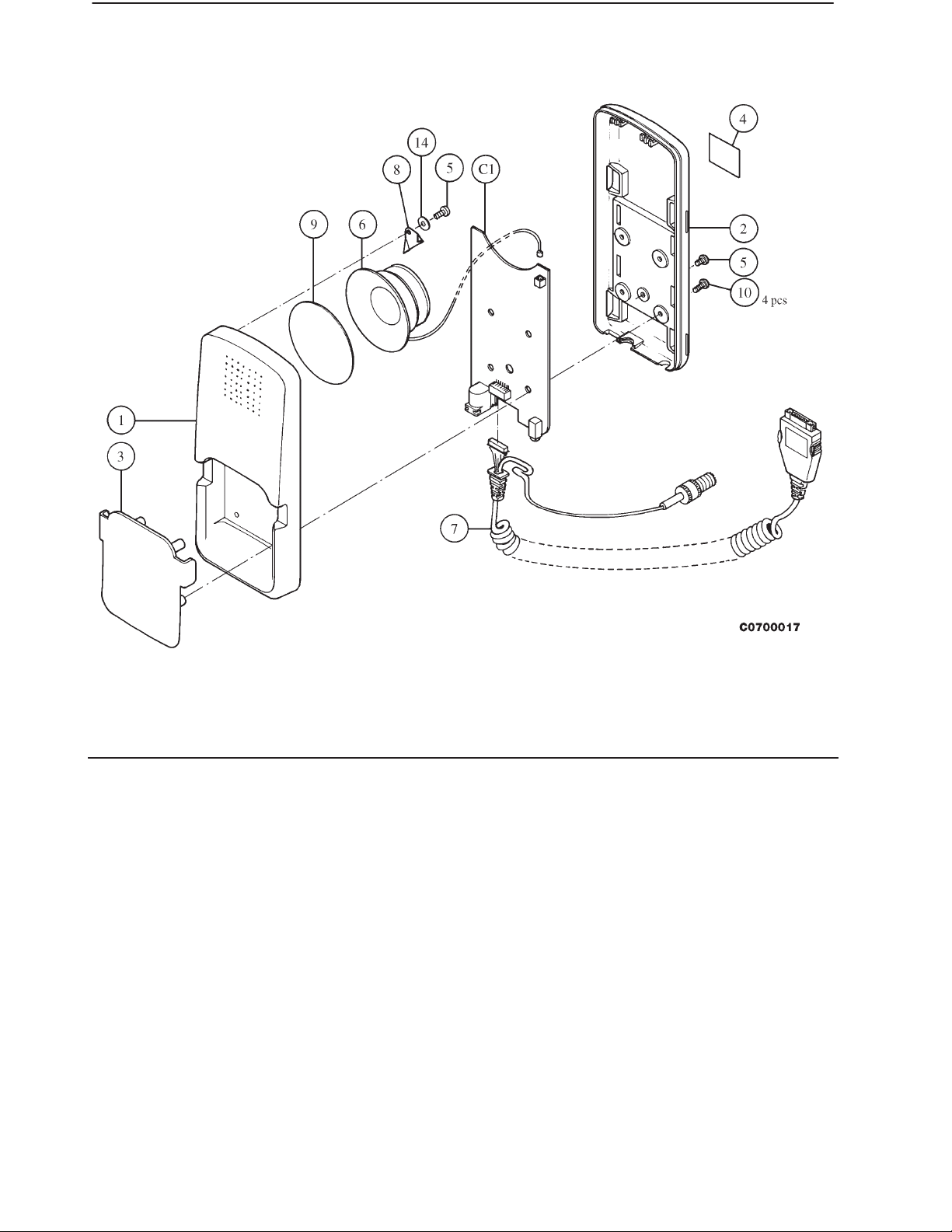
Exploded View
Technical DocumentationPHF–1
Assemply Parts
ITEM Q’TY CODE DESCRIPTION VALUE, TYPE
1 9450254 Cover A 1D 22196
2 9450255 Cover B 1D 22197
3 9450256 Cover C 2D 22198
4 9380154 Type label 4D 23477
5 2 6293012 PT screw KB22x8 FeZn clr
6 5140098 Speaker 4 Ω 5 W
7 9780087 Coax coil 4C22834
8 9303320 Cradle A4D 40109
9 9309555 Loudspeaker cloth A4D 40368
10 4 6293012 PT screw KB22x14 FeZn blk
C1 0200179 DH3 module
Page 16
Original 03/97
Page 2

Technical Documentation PHF–1
N100 4340108 IC, regulator L4810 10 V 0.4 A SOT194
N200 4301182 IC, 2 x op.amp. LM2902 SO14S
N300 4303440 IC, af amp+mute +4/30v dil1TDA1905 DIL16S
N401 4305236 IC, 2 x comp. LM2903 SO8S
N402 4301062 IC, regulator LP2951AC SO8S
X100 5414943 Dc–jack d6.3/2 pcb
X200 5407016 Jack stereo 2.5mm smd
X300 5416640 Pin header m1x2 p1.5 90deg 1a0r02 1A0R02
X400 5416638 Connector 8–pole right angle 1.5 1.5
9853924 PCB DH3 116.9X61.0X1.6 D 3/PA
9853924 PC board DH3 116.9x61.0x1.6 d 3/pa
Original 03/97
Page 15
Page 3

Technical DocumentationPHF–1
C403 2309517 Ceramic cap. 100 n 10 % 50 V 1206
C404 2309517 Ceramic cap. 100 n 10 % 50 V 1206
C405 2310544 Ceramic cap. 1.0 n 5 % 50 V 0805
C406 2310752 Ceramic cap. 10 n 20 % 50 V 0805
C408 2310752 Ceramic cap. 10 n 20 % 50 V 0805
C409 2604209 Tantalum cap. 1.0 u 20 % 16 V 3.2x1.6x1.6
C410 2502736 Electrol. cap. 220 u 20 % 16 V 3.5MM
C411 2310449 Ceramic cap. 150 p 5 % 50 V 0805
C501 2310505 Ceramic cap. 470 p 5 % 50 V 0805
C502 2310505 Ceramic cap. 470 p 5 % 50 V 0805
C503 2310505 Ceramic cap. 470 p 5 % 50 V 0805
C504 2310505 Ceramic cap. 470 p 5 % 50 V 0805
C505 2310505 Ceramic cap. 470 p 5 % 50 V 0805
C506 2320075 Ceramic cap. 470 p 5 % 50 V 0603
C507 2312410 Ceramic cap. 1.0 u 10 % 16 V 1206
C508 2310424 Ceramic cap. 100 p 5 % 50 V 0805
C509 2310424 Ceramic cap. 100 p 5 % 50 V 0805
C515 2501605 Electrol. cap. 100 u 20 % 35 V RM3.5
L001 0164030 Choke 9 u
L002 0164030 Choke 9 u
L400 3607555 Coil 125 u 2 A d17x12mm
L401 0164030 Choke 9 u
L501 3616705 Choke RI n 2 A
Z001 3640011 Filt z>600r/100m 0r6max 0.2a 0805 0805
V001 4103496 Trans. supr. 33V 400 V 5000 W d9.1xl9.1
V010 4210108 Transistor BSR20 pnp 12 V 0.6 A SOT23
V011 4107040 Zener diode BZX84 5 % 6.2 V 0.3 W SOT23
V012 4108639 Diode x 2 BAS28 75 V 250 mA SOT143
V014 4108639 Diode x 2 BAS28 75 V 250 mA SOT143
V020 4210106 Transistor BSR19 npn 14 V 0.6 A SOT23
V030 4210106 Transistor BSR19 npn 14 V 0.6 A SOT23
V040 4200610 MosFet p–ch 50 V 5.3 A TO252
V041 4107026 Zener diode BZX84 5 % 7.5 V 0.3 W SOT23
V202 4210106 Transistor BSR19 npn 14 V 0.6 A SOT23
V203 4100285 Diode x 2 BAV99 70 V 200 mA SER.SOT23
V400 4215954 MosFet RFD14N05 n–ch 50 V 10 A TO252
V401 4210106 Transistor BSR19 npn 14 V 0.6 A SOT23
V402 4210108 Transistor BSR20 pnp 12 V 0.6 A SOT23
V403 4108639 Diode x 2 BAS28 75 V 250 mA SOT143
V404 4108639 Diode x 2 BAS28 75 V 250 mA SOT143
V405 4110034 Schottky diode MBRS140 40 V 1 A DO214AA
V406 4107160 Zener diode BZX84 5 % 12 V 0.3 W SOT23
V407 4107027 Zener diode BZX84 5 % 16 V 0.3 W SOT23
V408 4108639 Diode x 2 BAS28 75 V 250 mA SOT143
V409 4108639 Diode x 2 BAS28 75 V 250 mA SOT143
V410 4200917 Transistor BC848B/BCW32 npn 30 V 100 mA SOT23
V411 4107160 Zener diode BZX84 5 % 12 V 0.3 W SOT23
V412 4107027 Zener diode BZX84 5 % 16 V 0.3 W SOT23
Page 14
Original 03/97
Page 4

Technical Documentation PHF–1
R407 1413635 Chip resistor 100 k 5 % 0.1 W 0805
R408 1415872 Melf resistor 120 1 % 0.2 W 0204
R409 1415600 Melf resistor 1.0 k 1 % 0.2 W 0204
R410 1411123 Melf resistor 0.22 5 % 0.2 W 0204
R411 1412423 Chip resistor 4.7 k 5 % 0.1 W 0805
R412 1415745 Chip resistor 3.32 k 1 % 0.12 W 1206
R413 1412423 Chip resistor 4.7 k 5 % 0.1 W 0805
R414 1411669 Chip resistor 22 5 % 0.1 W 0805
R415 1412416 Chip resistor 2.2 k 5 % 0.1 W 0805
C001 2310336 Ceramic cap. 18 p 5 % 50 V 0805
C011 2604431 Tantalum cap. 10 u 20 % 16 V 6.0x3.2x2.5
C012 2310784 Ceramic cap. 100 n 10 % 25 V 0805
C111 2503072 Electrol. cap. 470 u 20 % 16 V 10x16
C201 2604209 Tantalum cap. 1.0 u 20 % 16 V 3.2x1.6x1.6
C202 2310336 Ceramic cap. 18 p 5 % 50 V 0805
C206 2310336 Ceramic cap. 18 p 5 % 50 V 0805
C207 2310336 Ceramic cap. 18 p 5 % 50 V 0805
C208 2310336 Ceramic cap. 18 p 5 % 50 V 0805
C209 2310336 Ceramic cap. 18 p 5 % 50 V 0805
C210 2310336 Ceramic cap. 18 p 5 % 50 V 0805
C211 2310336 Ceramic cap. 18 p 5 % 50 V 0805
C212 2310336 Ceramic cap. 18 p 5 % 50 V 0805
C213 2604209 Tantalum cap. 1.0 u 20 % 16 V 3.2x1.6x1.6
C214 2310336 Ceramic cap. 18 p 5 % 50 V 0805
C215 2604209 Tantalum cap. 1.0 u 20 % 16 V 3.2x1.6x1.6
C216 2604209 Tantalum cap. 1.0 u 20 % 16 V 3.2x1.6x1.6
C217 2310449 Ceramic cap. 150 p 5 % 50 V 0805
C218 2604209 Tantalum cap. 1.0 u 20 % 16 V 3.2x1.6x1.6
C219 2604209 Tantalum cap. 1.0 u 20 % 16 V 3.2x1.6x1.6
C220 2310336 Ceramic cap. 18 p 5 % 50 V 0805
C231 2310720 Ceramic cap. 3.3 n 20 % 50 V 0805
C232 2310784 Ceramic cap. 100 n 10 % 25 V 0805
C233 2310336 Ceramic cap. 18 p 5 % 50 V 0805
C235 2310784 Ceramic cap. 100 n 10 % 25 V 0805
C236 2310784 Ceramic cap. 100 n 10 % 25 V 0805
C250 2310784 Ceramic cap. 100 n 10 % 25 V 0805
C251 2310336 Ceramic cap. 18 p 5 % 50 V 0805
C301 2502736 Electrol. cap. 220 u 20 % 16 V 3.5MM
C302 2310336 Ceramic cap. 18 p 5 % 50 V 0805
C303 2310784 Ceramic cap. 100 n 10 % 25 V 0805
C304 2604431 Tantalum cap. 10 u 20 % 16 V 6.0x3.2x2.5
C305 2310784 Ceramic cap. 100 n 10 % 25 V 0805
C306 2310784 Ceramic cap. 100 n 10 % 25 V 0805
C307 2604431 Tantalum cap. 10 u 20 % 16 V 6.0x3.2x2.5
C308 2310784 Ceramic cap. 100 n 10 % 25 V 0805
C309 2310784 Ceramic cap. 100 n 10 % 25 V 0805
C401 2309517 Ceramic cap. 100 n 10 % 50 V 1206
C402 2501605 Electrol. cap. 100 u 20 % 35 V RM3.5
Original 03/97
Page 13
Page 5

Technical DocumentationPHF–1
Parts List EDMS issue 1.2 Code: 0200179
ITEM CODE DESCRIPTION VALUE TYPE
R011 1413635 Chip resistor 100 k 5 % 0.1 W 0805
R012 1412536 Chip resistor 22 k 5 % 0.1 W 0805
R013 1413635 Chip resistor 100 k 5 % 0.1 W 0805
R015 1412430 Chip resistor 10 k 5 % 0.1 W 0805
R021 1413635 Chip resistor 100 k 5 % 0.1 W 0805
R022 1413635 Chip resistor 100 k 5 % 0.1 W 0805
R031 1413635 Chip resistor 100 k 5 % 0.1 W 0805
R032 1412430 Chip resistor 10 k 5 % 0.1 W 0805
R041 1413635 Chip resistor 100 k 5 % 0.1 W 0805
R201 1413635 Chip resistor 100 k 5 % 0.1 W 0805
R202 1413635 Chip resistor 100 k 5 % 0.1 W 0805
R212 1413635 Chip resistor 100 k 5 % 0.1 W 0805
R213 1412416 Chip resistor 2.2 k 5 % 0.1 W 0805
R214 1414029 Chip resistor 3.3 k 5 % 0.1 W 0805
R215 1414131 Chip resistor 180 k 5 % 0.1 W 0805
R216 1414212 Chip resistor 330 k 5 % 0.1 W 0805
R217 1414283 Chip resistor 100 k 1 % 0.1 W 0805
R220 1414283 Chip resistor 100 k 1 % 0.1 W 0805
R221 1412430 Chip resistor 10 k 5 % 0.1 W 0805
R222 1412335 Chip resistor 1.0 k 5 % 0.1 W 0805
R223 1412430 Chip resistor 10 k 5 % 0.1 W 0805
R224 1412430 Chip resistor 10 k 5 % 0.1 W 0805
R225 1412430 Chip resistor 10 k 5 % 0.1 W 0805
R226 1414283 Chip resistor 100 k 1 % 0.1 W 0805
R227 1414283 Chip resistor 100 k 1 % 0.1 W 0805
R231 1414283 Chip resistor 100 k 1 % 0.1 W 0805
R232 1414283 Chip resistor 100 k 1 % 0.1 W 0805
R233 1414283 Chip resistor 100 k 1 % 0.1 W 0805
R234 1414283 Chip resistor 100 k 1 % 0.1 W 0805
R235 1414109 Chip resistor 15 k 5 % 0.1 W 0805
R236 1412430 Chip resistor 10 k 5 % 0.1 W 0805
R301 1413829 Chip resistor 10 5 % 0.1 W 0805
R302 1413829 Chip resistor 10 5 % 0.1 W 0805
R303 1412261 Chip resistor 100 5 % 0.1 W 0805
R304 1412416 Chip resistor 2.2 k 5 % 0.1 W 0805
R305 1412261 Chip resistor 100 5 % 0.1 W 0805
R308 1414109 Chip resistor 15 k 5 % 0.1 W 0805
R309 1412430 Chip resistor 10 k 5 % 0.1 W 0805
R401 1415784 Melf resistor 4.75 k 1 % 0.2 W 0204
R402 1413635 Chip resistor 100 k 5 % 0.1 W 0805
R403 1411669 Chip resistor 22 5 % 0.1 W 0805
R404 1412423 Chip resistor 4.7 k 5 % 0.1 W 0805
R405 1413635 Chip resistor 100 k 5 % 0.1 W 0805
Page 12
Original 03/97
Page 6

Technical Documentation PHF–1
Layout Diagrams of DH3
Original 03/97
Page 11
Page 7

Circuit Diagram of DH3
Technical DocumentationPHF–1
Page 10
Original 03/97
Page 8

Technical Documentation PHF–1
Block Diagram
Original 03/97
Page 9
Page 9

Audio Section
V202, R201 and R202 generates +5VA audio d.c. voltage. V202 is the microphone voltage regulator. N200 is the mic. amplifier. N200 is the differential amplifier wich eliminates disturbancies generated in curly cable ground wire resistor. N200 has same function in XEAR line. R235 and C231 are low pass filter
wich eliminates noise. N300 is speaker power amplifier. R302, R303 and C303
stabilicies the power amplifier in high frequencies.
Technical DocumentationPHF–1
Page 8
Original 03/97
Page 10

Technical Documentation PHF–1
System Connector X400
Pin Name Description
1 VC Supply voltage
2 M2BUS Serial bidirectional data control.
3 PHFS HF device power on/off
4 GND Ground
5 AGND Audio ground.
6 XEAR/HFJPWR Ext. audio/HF junction box identification.
7 XMIC/JCONN Ext. mic./HF box connection control signal.
8 AGND Audio ground.
Circuit Description
Input Circuit
C1 is the EMI capacitor. F1 is the foil fuse. L1 and L2 are EMI suppressor
chokes. V1 is the voltage suppressor diode (zener type).
Power Control Logic
Input power is connected to d.c. connector X100. Power is connected to audio
devices thru P–FET V410 and 10 V regulator N100 (VBSW). This power is connected when M2BUS signal goes high. Also XEAR signal can connect power
on 5 sec by grounding it with 100 kΩ resistor, wich is located inside the phone.
Same 5 sec power on time occurs also, when MBUS and XEAR are low and
input power occurs to d.c. connector. C11 acts like a timing capacitor.
Switched Mode Power Supply
The WBSV voltage generated by N100 starts the switched mode power supply
(SMPS) by starting reference regulator N402. V409 leads the initial current to
totally empty battery. V410 is an constant current source wich sets the voltage
value of R408. Same voltage occurs over the current shunt resistor R410,
when the SMPS is working. N401a is an pulse width modulator. N401b with
R407,C408 and V408 generates a minimum pulse width of SMPS. R405 and
R406 are input and output voltage correction resistors. V412 shutdowns the
SMPS when VB input voltage goes over 17 V. V407 limits the comparator power supply VCC. V408 and V406 limits the comparator output voltage. V403 and
C403 consist an bootstrap circuit, wich act like voltage doubler. V400 is the
SMPS switch. L401 (L402), R403 and C405 are EMI suppression components.
L400 is the main SMPS inductor. V411 limits the maximum output voltage.
Original 03/97
Page 7
Page 11

External Signals and Connections
The module has four external connectors, the power supply connector, HF microphone connector, HF speaker connector and system connector.
Power Supply Connector X100
Pin Name Description
1 VC Supply voltage
2 GND Ground
HF Microphone Connector X200
Pin Name Description
Technical DocumentationPHF–1
• pwr off current: 0.8...1 mA
• pwr on/no charging current: 50...90 mA
• pwr on/charging current: 600...800 mA
1 GND Ground
2 HFMIC Microphone signal
HF Speaker Connector X300
Pin Name Description
1 HFSP Speaker signal
2 GND Ground
• output voltage: 5.0...5.8 V
• intrnal resistance: 2200 Ω
• input impedance: 1000 Ω
• load impedance: 4 Ω
• output power: 3 W
Page 6
Original 03/97
Page 12

Technical Documentation PHF–1
The phone is connected to the unit by a system connector. There are also connectors for external power source, for standard HF–microphone and for external antenna(s).
The Compact Handsfree Holder consists of speaker– and microphone– amplifiers, power on/off –logic, HF–speaker muting and the constant current switching regulator for charging the phone battery. The unit has an inbuilt HF–speaker and an external HF–microphone but the actual handsfree function is
generated in the phone.
MPHF1 mechanic consists of the front and rear covers, the holder cover,
The
screws, type label, system–cable with RF–cable(s).
Modes of Operation
Power off: The DH3 module does not receive supply voltage
to the d.c. connector (X100 so there aro not any
voltages on the module.
Standby: The module receives supply voltage to the d.c.
connector but the telephone has put the M2BUS line
(X400) down (”0”–state) because the phone is off and
the battery is fully charged. The switching regulator in
off and there is not any supply voltage for the audio.
Power on/ The M2BUS –line is high (”1”–state) so the switching
speaker off: regulator supplies charging current to the phone. The
supply voltage for the audio is on but the PHFS –line
(X400) is down (”0”–state) so the HF–speaker is muted.
Power on/ The switching regulator supplies charging current to
speaker on the phone. The supply voltage for the audio is on and
the PHFS–line is high (”1”–state) so the HF–speaker
is on.
Original 03/97
Page 5
Page 13

Compact HF Holder PHF–1
Introduction
The PHF–1 is compact handsfree holder for the second generation digital
handportable telephones and they provide possibility to use handsfree operation where the fixed handsfree configuration is not possible. They have also
phone battery charging function.
Technical DocumentationPHF–1
Technical Summary
The installation to the car is possible by four separate methods. Using the separate mounting plate, strechable bands, adhesive tape, or ”velco straps”.
The configuration allows both the handsfree– and the handset–use of the
phone. The handset–use is possible with the curly system cable which includes
also the antenna cable(s). The separation of the HF– and hs–mode is made by
the hook–switch in the holder .
Page 4
Original 03/97
Page 14

Technical Documentation PHF–1
COMPACT HANDSFREE HOLDER PHF–1
Contents
Compact HF Holder PHF–1 Page 4. . . . . . . . . . . . . . . . . . . . . . . . . . . . . .
Introduction Page 4. . . . . . . . . . . . . . . . . . . . . . . . . . . . . . . . . . . . . . . . . .
Technical Summary Page 4. . . . . . . . . . . . . . . . . . . . . . . . . . . . . . . . . . .
Modes of Operation Page 5. . . . . . . . . . . . . . . . . . . . . . . . . . . . . . . .
External Signals and Connections Page 6. . . . . . . . . . . . . . . . . . . .
Power Supply Connector X100 Page 6. . . . . . . . . . . . . . . . . . . .
HF Microphone Connector X200 Page 6. . . . . . . . . . . . . . . . . . .
HF Speaker Connector X300 Page 6. . . . . . . . . . . . . . . . . . . . . .
System Connector X400 Page 7. . . . . . . . . . . . . . . . . . . . . . . . . .
Circuit Description Page 7. . . . . . . . . . . . . . . . . . . . . . . . . . . . . . . . . . . .
Input Circuit Page 7. . . . . . . . . . . . . . . . . . . . . . . . . . . . . . . . . . . . . . .
Power Control Logic Page 7. . . . . . . . . . . . . . . . . . . . . . . . . . . . . . . .
Switched Mode Power Supply Page 7. . . . . . . . . . . . . . . . . . . . . . .
Audio Section Page 8. . . . . . . . . . . . . . . . . . . . . . . . . . . . . . . . . . . . . .
Block Diagram Page 9. . . . . . . . . . . . . . . . . . . . . . . . . . . . . . . . . . . . . . .
Circuit Diagram of DH3 Page 10. . . . . . . . . . . . . . . . . . . . . . . . . . . . . . . .
Layout Diagrams of DH3 Page 11. . . . . . . . . . . . . . . . . . . . . . . . . . . . . .
Parts List EDMS issue 1.2 Code: 0200179 Page 12. . . . . . . . . . . . . .
Exploded View Page 16. . . . . . . . . . . . . . . . . . . . . . . . . . . . . . . . . . . . . . .
Assemply Parts Page 16. . . . . . . . . . . . . . . . . . . . . . . . . . . . . . . . . . . . . .
Original 03/97
Page 3
Page 15

Technical DocumentationPHF–1
AMENDMENT RECORD SHEET
Amendment
Number
Date Inserted By Comments
Page 2
Original 03/97
Page 16

COMPACT HANDSFREE
HOLDER PHF–1
Original 03/97
 Loading...