

Page 1

TROUBLESHOOTING
NHE–1
Contents
Troubleshooting 6–2–2
General 6–2–2
Flash Programming OK; part 1 6–2–3
Flash Programming OK; part 2 6–2–4
Flash Programming OK; part 3 6–2–5
Flash Programming OK; part 4 6–2–6
PWR Button Fault 6–2–7
Display Selftest Failed 6–2–8
No Registration to the System (no svc) 6–2–9
Audio Fault 6–2–10
Power Up Sequence 6–2–11
Repairing Instructions for Flash Faulty Units 6–2–12
RF Tuning Fails 6–2–14
Synthesizer Fails; part 1 6–2–16
Synthesizer Fails; part 2 6–2–17
RX Signal levels 6–2–18
9711OJ
Technical Documentation
6–2–1
Copyright Nokia Mobile Phones
ORIGINAL 1 1/97
Page 2

TROUBLESHOOTING
NHE–1
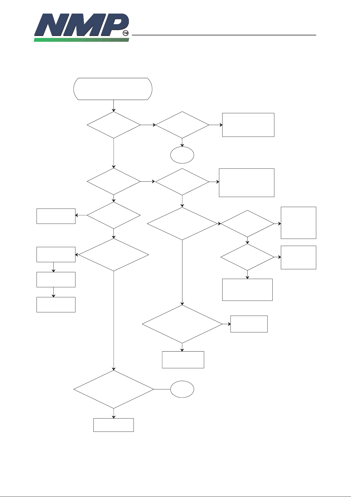
Troubleshooting
General
The purpose is to define fault block of the module and then find out the broken component. The trouble shooting diagram has been planned so that the fault, whatever
it is, can be found by as simple measurements as possible.
The flow diagrams give you the overview of the blocks. The purpose is that you
proceed through the flow diagram so that, if your answer is YES for the asked
question, go straight to the next level, but if your answer is NO, you have to go
the subbranch.
Required servicing equipment:
– PC for Service Software
– Power supply (2.0 A)
– Digital multimeter
9711OJ
Technical Documentation
6–2–2
Copyright Nokia Mobile Phones
– Oscilloscope
– Spectrum analyzer
– RF cables
– Modular cable
– RS232/MBUS adapter
– CMT/Marconi
– RF measuring chassis
ORIGINAL 1 1/97
Page 3
TROUBLESHOOTING
NHE–1
9711OJ
Technical Documentation
Flash Programming OK; part 1
FLASH programming OK
YES
YES
Check X100
C113 OK?
YES
R110 OK?
YES
MBUS
registration
OK?
Power
stays on?
NO
NO
NO
VBATT
pins 5, 20?
YES
N271/pin 8/XRESET
+5 V after pwr on?
Display:
selftest failed
YES
3
Display:
selftest failed
YES
MBUS line X100/5
+5 V after pwr on?
YES
NO
NO
Copyright Nokia Mobile Phones
D231/MCU/pin 3
D230/ASIC/pin 97
rstrobe
Short circuits in data
data lines. data line
disconnected, VREF
unconnected
NO
R166
+ 5 V?
YES
V160 base
∼1 V
YES
Check R163,
V160, R161,
R160, C160
If D231 at
NO
pin 66/TXD
doesn’t apply
+5 V change
NO
R165, R166
V161, R164
6–2–3
D231
Check
Change N271
ORIGINAL 1 1/97
Power supp. to the logic
circuits +5 V after pwr on?
NO
Change N271
MCU/D231/PIN67/RDX
+5 V after pwr on (J109)?
NO
If R162 is OK
change D231
YES
2
YES
Change first
D231
Page 4

TROUBLESHOOTING
NHE–1
9711OJ
Technical Documentation
Flash Programming OK; part 2
NO
RESETX +5 V after
YES
Change D230
26 MHz clock
D230/pin 119?
NO
26 MHz/1 Vpp in
testpoint J113
2
MCU/D231/pin 10
power on?
/pin 8/MD2, MCU/D230
Copyright Nokia Mobile Phones
YES
26 MHz at MCU
/D230 pin 69
/MCUCLK?
YES
MCU/D230
/pin 9/STNDBY?
NO
Change D230
NO
6–2–4
Check joints
and foils
YES
Check components
D191, D192, R231
R246, R247, C234
YES
MCU/D231/pin 43
/XPWROFF pulses up to
+5 V after pwr on?
YES
MCU/D231/pin 77
/IRQ0 +5 V after
power on?
YES
MCU/D231/pin 4
/WSTROBEX +5 V
after pwr on?
YES
Check all soldered joints
The data and address signals must
a clear difference between low (0 V)
and high (+5 V)
NO
NO
NO
Change D231
Change D230
Check D230
ORIGINAL 1 1/97
Page 5
TROUBLESHOOTING
NHE–1
9711OJ
Technical Documentation
Flash Programming OK; part 3
MBUS registration OK?
Display: selftest failed?
3
YES
YES
EEPROM
initialization OK?
(FLASH8N.MES)
NO
6–2–5
Copyright Nokia Mobile Phones
YES
4
Check D230
Check D231
(D230)
Check D231
(D230)
NO
NO
NO
D184/EEPROM
/pin 27/EROMSELX pulses
+5 to 0 V during r/w
action?
YES
D184/EEPROM
/pin 1/RSTROBEX pulses
+5 to 0 V during r/w
action?
YES
D184/EEPROM
/pin 1/WSTROBEX pulses
+5 to 0 V during r/w
action?
YES
Change D184
ORIGINAL 1 1/97
Page 6

TROUBLESHOOTING
NHE–1
9711OJ
Technical Documentation
Flash Programming OK; part 4
/pin 11 +12 V during
/pin 64/HOOK/RXD2
pulses during prog?
/PHFS/TXD2 pulses
during programming?
4
D185/FLASH
programming?
YES
D231/MCU
YES
X100/pin 7
Copyright Nokia Mobile Phones
NO
NO
NO
Check X100/pin 14
C182, R175, R169
Check X100/pin 6
R177, R178, C176
Check D231/pin63
R184, R185, C186
6–2–6
Check D185/FLASH/
ADDRESS/DATA LINES
/no shortcircuits or
unconnected pins allowed
OK
YES
D185/FLASH
/pin 12/PWD +5 V
after power on?
YES
D185/FLASH
/pin 9/ROMSELX pulses
from +5 to 0 V after
power on?
YES
/pin 37/RSTROBEX pulses
YES
/pin 38/WSTROBEX pulses
D185/FLASH
from +5 to 0 V after
power on?
D185/FLASH
from +5 to 0 V after
power on?
NO
NO
NO
NO
Check D230
Check D231 (D230)
Check D231 (D230)
Check D231 (D230)
Change D185
ORIGINAL 1 1/97
Page 7

TROUBLESHOOTING
NHE–1
PWR Button Fault
Change
FLEX OK
9711OJ
Technical Documentation
Nothing happens when
PWR button is pressed
N271/PSL
pin 10 +5 V when VBATT
VBATT is connected
YES
N271/PSL
pin 10 +5–>0 V when
push PWR button
6–2–7
Copyright Nokia Mobile Phones
Check
X100
NO
NO
N271/PSL pins 5,2
VBATT voltage
YES
Change
N271
Check
X196
YES
R110, C113
OK
Check component
around N271 if OK
change N271
ORIGINAL 1 1/97
Page 8

TROUBLESHOOTING
NHE–1
Display Selftest Failed
9711OJ
Technical Documentation
Display selftest failed or
phone doesn’t registrate to
the system (tester)
Use PCLocals to
find out a reason
MCU internal test
MCU RAM bus test
MCU ROM bus test
MCU IMEI test
NO
Copyright Nokia Mobile Phones
YES
Unprogrammed FLASH
Unconnected pins in MCU
address or data lines
6–2–8
MCU DSP code
download: failed,
DSP tests: no responce
RFI bus fault
NO
MCU audio codec
test: failed
YES
Codec N260/pin 12 : PCMDO
Codec N260/pin 13 : PCMDI
Codec N260/pin 19 : PCMCLK
Codec N260/pin 20 : XSELPCMC
YES
DSP clock oscillator
DSP pin 45/INT1
DSP pin 10/ERAMHI
DSP pin 9/IOX
DSP pin 12/EROM
DSP pin 14/RWN
DSP pin 15/RWN
DSP pin 39/RSTB
RFI/RFIAD 3:0
RFI/RFIDA 11:0
RFI pin 49/RDX
RFI pin 50/WRX
RFI pin 53/RFICLK
RFI pin 59/RFI2CLK
DSP RAM D210, D211
DSP/DSPDA
DSP/DSPAD
ORIGINAL 1 1/97
Page 9

TROUBLESHOOTING
NHE–1
9711OJ
Technical Documentation
No Registration to the System (no svc)
No registration to the
system (no svc)
no call
Selftest OK
YES
DSP pin 43, 45 INT0, 1 (from ASIC)
RFI pins 1,63/RXI, RXQ
RFI pin 3/EXTBG (4.096 V)
RFI pin 4/VCM (2.35 V)
RFI pin 6/TXC (to RF)
RFI pins 8,9/TXQ+, TXQ– (to RF)
RFI pins 11,12/TXI+, TXI– (to RF)
RFI pin 14/AFC (to RF)
RFI pins 20...23,28,29/PDA TA 5:0
RFI pin 51/DAX (to ASIC)
ASIC/D230/pin 105/SYNTHPWR (to RF)
ASIC/D230/pin 104/TXP (to RF)
ASIC/D230/pin 106/TXPPWR (to RF)
ASIC/D230/pin 111/SENAT (to RF)
ASIC/D230/pin 112/SENAR (to RF)
ASIC/D230/pin 113/SDAT (to RF)
ASIC/D230/pin 114/SCLK (to RF)
6–2–9
Copyright Nokia Mobile Phones
ORIGINAL 1 1/97
Page 10

TROUBLESHOOTING
NHE–1
Audio Fault
9711OJ
Technical Documentation
Audio fault
Microphone or earphone
signal missing
Microphone and
earphone signal
missing?
NO
Microphone signal
missing?
YES
YES
6–2–10
Copyright Nokia Mobile Phones
CODEC pin 15/SYNC (from ASIC)
CODEC pin 16/CODEC_CLK (from ASIC)
DSP pins 79, 82/PCMCOSYCLKX (from ASIC)
DSP pins 60, 81/PCMDATRCLKX (from ASIC)
DSP pin 80/CODEC_CLK
CODEC N260/pins 22, 23 MICP, MICN
X196/pins 18, 19 MICP, MICN
CODEC N260/pin 10 PCMOUT
CODEC N260/pin 17 MICENA
X196/pin 12 MICENA
NO
Earphone signal
missing?
YES
CODEC N260/pins 6, 7
X196/pins 20, 21
CODEC N260/pin 14/PCMIN
DSP D200/pin 78
ORIGINAL 1 1/97
Page 11

TROUBLESHOOTING
NHE–1
Power Up Sequence
VBAT 5.5...8 V
CHRGDET 1.5 V
DETIN
ON
5,20
11
12
14
XPWROFF
C113
9
9711OJ
Technical Documentation
VCTCXO
CLK 26 MHz
D192
VL1 MCU CLK
VL2
VREF
1
VA
2
VA2
24
XRESET
846
ASIC MCUPSL
BUFFER
CLK 26 MHz
116
RESET
45
IRQX
99
5 V=ON
6–2–11
Copyright Nokia Mobile Phones
69
10
77
5,42 66
43
TXD
R166
XPWROFF 2 Hz
PSL
– Output voltages must be stay at high state at least 1.5 s when power is
switched on.
– If no; check C113.
– If it is OK; replace PSL.
– If the XRESET line doesn’t rise check CHRDET and DETIN. The voltage
value at these pins should be 1.5 V.
ASIC
– When XRESET and CLK are supplied to the ASIC but MCUCLK or RESETX
to the MCU are not supplied; replace ASIC.
MCU
– If MCUCLK and RESETX are supplied from ASIC but TXD line (MBUS)
doesn’t rise and solderings of the MCU are good; replace MCU.
– If TXD pin (MCU) goes to high but doesn’t stay at high state at least 1.5 s.
ORIGINAL 1 1/97
The power of the phone can be hold on following way:
– Connect PSL pin 14 to the ground.
– Lift MCU pin 77 IRQ0 and connect it to VL1.
Now its possible to use Service software.
Page 12

TROUBLESHOOTING
NHE–1
9711OJ
Technical Documentation
Copyright Nokia Mobile Phones
Repairing Instructions for Flash Faulty Units
1. When the phone doesn’t start (power off after 2 seconds) check following things:
– VBATT is connected to the PSL N271
– XRES rise to high state
– VL1 is 4.7 V
– VREF is connected to the VCTCXO and the crystal is running frequency is
26 MHz
Measure:
– supply voltage of MCU D231
– reset signal for MCU (RESETX) rise high state
– MCU clocksignal is 26 MHz
– NMI line stay low
– IRQ0 rise high state
6–2–12
If things (mentioned above) are ok, the MCU starts supply poweroff pulses to
the PSL N271 and the power stay on.
Most likely IRQ0 stay low, which means that interrupt is generated all the time.
In these cases check data and addresslines of MCU’s and memory circuits.
There are shortcircuits or unconnected pins.
The power can be forced stay on by connected PSL N271 pin 14 to the ground.
2. When FLASH PROGRAMMING is not succeed, check following things:
– System connector X100 pins 6, 7, 14 are soldered and there are no shortcir-
cuits.
– Flash programming voltage (12 V) is connected to D185 pin 11.
– The data and addresslines of flashcircuit D185 are soldered.
– EEPROM D184 should be OK because of the initialization (program param-
eters are loaded always when program is loading the first time).
3. When FACTORY SET is not succeed or the power is switched off after programming:
When power is switched on the program of the phone will start so called maxi-
mum mode and if this doesn’t work there was happened mistake during the
flash programming.
ORIGINAL 1 1/97
Page 13

TROUBLESHOOTING
NHE–1
9711OJ
Technical Documentation
Copyright Nokia Mobile Phones
4. If selftest (A) is failed, check:
– Solderings of EEPROM D184
– Do factory set once again (setup error in EEPROM D184)
5. If selftest (B) is failed, check:
– Measure by oscilloscope that crystal XT1 is running (60.2 MHz).
– Reset signal DSP1RSTX for DSP (D200 pin 39) is high state.
– Small clock signal at pins 37, 38 of DSP is greater than 400 mV
PP.
– Clock signal at pin 40 (DSP) is 30 MHz (square wave; amplitude 5 V).
– Check solderings of D200, D210 and D211.
6. If the phone takes too small current measure at pins of synthesizers that they are
working normally. Voltage at pin 8 should be 2 V.
7. If the phone takes too high current check the outputs of RF regulators that supply
voltages are OK.
6–2–13
ORIGINAL 1 1/97
Page 14

TROUBLESHOOTING
NHE–1
RF Tuning Fails
Calib Temperature Sensor
a) Check R770 and R173
b) Check D231 pin 56
AFC Fails
a) Check AFC control voltage; G701 pin 7 = 2.2 V
b) Check VCO’s control voltage; C8511, C748 = 2.2 V (see synthesizer fails)
c) Check RX branch gain (see RX signal levels)
d) If a, b and c is OK then check solders of N270 –> change N270
RSSI Fails
RSSI Offset Value Fail
9711OJ
Technical Documentation
6–2–14
Copyright Nokia Mobile Phones
a) Check RX branch gain (see RX signal levels)
b) check solders of N270, D200 and D230
RSSI 12 dB NIF Fail (others OK)
a) Check solders of N702 and surrounding components of N702
RSSI 24 dB Fail (others OK)
a) Check R712
b) Check solders of N704
RSSI 12 dB, 24 dB and 36 dB Fail (others OK)
a) Check R712
b) Check solders of N704
RSSI 3 dB...45 dB Fails
a) Check N704
b) Check N270
RSSI 3 dB...45 dB and RSSI offset value fails
a) Check RX branch gain (see RX signal levels)
b) Check solders of N270, D200 and D230
ORIGINAL 1 1/97
Page 15

TROUBLESHOOTING
NHE–1
TXI/TXQ Tuning
Carrier leagage must be tuned with shields on and middle screws tighten.
Upper side bands amplitude is not allowed to tune to its minimum with ampli-
tude and phase tuning. Because if the data type is changed to another then the
USP signal will be higher => TUNE TO BALANCE.
If there is not signal at N803’s pins 10...13 then check N270’s solders.
IF there is not signal at N803’s output pins 15 and 16 => check input level at
pins 5 and 6 and control pulse at pin 1 .
Power Measuring
If there is not enough power at outputs then check
– solders of coaxpipes and bottom RF connector
– input level of RF signal N801’s pin 1
– control signal from power control loop at N801’s pin 1
– input level at SAW filter Z802
– signals TXC at C866, TXP at R830, TXPWR to V817 to power control loop
9711OJ
Technical Documentation
6–2–15
Copyright Nokia Mobile Phones
Power Tuning
Tune TXC values at TX levels 5, 13 and 15.
Calib BATT_VOLTAGE = 6.0 V
a) Check R112, R113
b) Check N271 pin 23
c) Check D231 pin 52
Calib CHARGE_VOLTAGE = 6.0 V
a) Check R140, R142
b) Check D231 pin 53
ORIGINAL 1 1/97
Page 16

TROUBLESHOOTING
NHE–1
Synthesizer Fails; part 1
Synthesizer
Fails
Reg. supply voltages
check N802,N804
pin 8 4.7 V?
YES
Are VCO’s locked
to channels, check control
volt. C851,C748
2.2 V?
CONTROL
VOLTAGE 0 V
Check volt. of the PLL
(N806/N703)
pin 6,11=4.6 V
pin 13=1.1 V
pin 1,8=2.1 V (if 0 V
check control lines
SCLK,SDAT,SENAR/T)
OK
Check Fref (VCTCXO
signal) pin 1=25 MHz
> 1 Vpp
OK
Change IC
NO
CONTROL
9711OJ
Technical Documentation
Check voltages
pin 1/VBATT, pin 2/4.5 V
check shortcircuits
at pin 8
UHF–VCO
Check that control volt.
is the same in C851 and
in G800/pin 1
OK
Check with spect.
analyser that there is a
sign. in VCO’s G800/5
1040 MHz?
YES
Check that there is
same output signal in
N805/1?
YES
Copyright Nokia Mobile Phones
OK
Change regulator
2
Check VCO’s supply
NO
voltage pin 4 (4.6 V) and
solders of pins
Change VCO
NO
Check R838 and C850
6–2–16
VHF–VCO
OK
ORIGINAL 1 1/97
Check that there is
16 MHz pulses (A<1 Vpp)
in N805/4,N806/8?
YES
Change N806
Check supply voltages
NO
and solders of N805
OK
Change N805
Page 17

TROUBLESHOOTING
NHE–1
Synthesizer Fails; part 2
Check that control volt.
is the same in C748
and V707
OK
Check supply voltage
of V707; collector=4.6 V
and emitter=1.2 V
OK
Check output sign.
of the VCO (f>245 MHz)
in N702/pin 6?
9711OJ
Technical Documentation
2
NO
Check surrounding
components of V707
6–2–17
Copyright Nokia Mobile Phones
YES
Check volt. of the RX–IC
(N702)
pin 15=4.6 V
pin 6=1.7 V
pin 24=4.6 V
pin 22,23=3.7 V (if 0 V
then there is a short circ.
in neither C747 or T700)
OK
Check T700/1,3,6;
VCO output sign divided
by 2 and same sign.
N703/8?
YES
Change N703
NO
Check solders of N702
OK
Change N702
ORIGINAL 1 1/97
Page 18

TROUBLESHOOTING
NHE–1
RX Signal levels
Levels were measured with High frequency passive probe 50 Ω 1:1
The phone is connected to the spectrum analyzer via 0.18 µ blocking cap
and 6 dB attenuator. * Amplitude reference offset 10 dB (Pg = –10 dB)
Setting of Service software
Active unit: RX
Operation mode: Continuous
Continuous Mode: Channel 60
AGC: 93 dB
Signal Levels at Front End
Signal (–50 dBm, f=947.0677 MHz) will be connected to the antenna connector.
Test point Position Frequency *Level Note:
1 V702 C 947.0 MHz –48 dBm Pg = –10 dB
2 V760 C 947.0 MHz –40 dBm Pg = –10 dB
3 N702 19 1018.0 MHz –3 dBm Pg = –10 dB
9711OJ
Technical Documentation
6–2–18
Copyright Nokia Mobile Phones
Signal Levels at IF
Signal (–80 dBm, f=947.0677 MHz) will be connected to the antenna connector.
Test point Position Frequency *Level Note:
4 C713/Z706 70.932 MHz –60 dBm Pg = –10 dB
5 N704 13 70.932 MHz –76 dBm Pg = –10 dB
6 N702 8 70.932 MHz –33 dBm Pg = –10 dB
7 N702 6 232.00 MHz –20 dBm Pg = –10 dB
8 N702 12 12.932 MHz –18 dBm Pg = –10 dB
9 RXQ or RXI 12.932 MHz –24 dBm Pg = –10 dB
ORIGINAL 1 1/97
 Loading...