

Page 1

SYSTEM MODULE DS9
NHK–1
9712OJ
Technical Documentation
Contents of System Module DS9
System module DS9 8–2
Introduction 8–2
Technical section 8–2
External and internal connectors 8–2
Internal signals between RF and ASIC 8–5
Internal signals between RF and RFI 8–6
Baseband block 8–7
Interconnection diagram 8–7
Technical specifications 8–7
Functional descriptions 8–8
Names of functional blocks 8–10
RF block 8–26
Functional description 8–26
Block diagram of baseband 8–29
Block diagram of RF 8–30
Power distribution diagram 8–31
Connections between system and RF blocks 8–32
Parts list of DS9 8–33
8–1
Copyright Nokia Mobile Phones
Circuit Diagram of DS9; System Blocks A3/8–1
Circuit Diagram of DS9; CPU and Memories (Version 4.5 edit 65) A3/8–2
Circuit Diagram of DS9; Power Supply IC & Battery Charg. Unit A3/8–3
Circuit Diagram of DS9; Audio Codec IC A3/8–4
Circuit Diagram of DS9; DSP, Clock Generator & Memories A3/8–5
Circuit Diagram of DS9; ASIC IC (Version 4.5 edit 68) A3/8–6
Circuit Diagram of DS9; RFI IC (Version 4.5 edit 40) A3/8–7
Circuit Diagram of DS9; RF Receiver A3/8–8
Circuit Diagram of DS9; RF Receiver (Version 4.3 edit 52) A3/8–9
Circuit Diagram of DS9; RF Transmitter A3/8–10
Circuit Diagram of DS9; RF Transmitter (Version 4.3 edit 94) A3/8–11
Layout Diagrams of DS9 Side 1 A3/8–12
Layout Diagrams of DS9 Side 2 A3/8–13
Layout Diagrams of DS9 Side 1 (Version 13) A3/8–14
Layout Diagrams of DS9 Side 2 (Version 13) A3/8–15
Page 2

SYSTEM MODULE DS9
NHK–1
System module DS9
Related documentation
Introduction
DS9 is the baseband/RF module NHK–1 cellular tranceiver. The DS9 module
carries out all the system and RF functions of the tranceiver. System module
DS9 is designed for a handportable phone, that operate in PCN system.
Technical section
9712OJ
Technical Documentation
8–2
Copyright Nokia Mobile Phones
All functional blocks of the system module are mounted on a single multi layer
printed circuit board. The chassis of the radio unit contains separating walls for
baseband and RF. All components of the baseband are surface mountable. The
connections to accessories are fed through the bottom connector of the radio
unit. The connections to user interface –module (UIF) are fed through a flex
connector. There is no physical connector between RF and baseband.
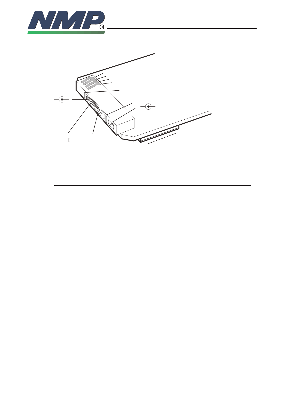
External and internal connectors
The system module has two connector, external bottom connector and internal
UIF module connector.
Page 3
SYSTEM MODULE DS9
NHK–1
Bottom connector X100
Antenna
connector
2
1
16
System connector
9712OJ
Technical Documentation
4
Battery connector
3
2
1
4
Charging connector
X100
9
18
3
30
12
X196
UIF module connector
Copyright Nokia Mobile Phones
1
D0000323
8–3
System connector
Pin: Name: Description:
1, 9 GND Digital ground
2 MIC/JCONN External audio input from accessories or
3 AGND Analog ground for accessories.
4 TDA Transmitted DBUS data to the accessories.
5 M2BUS Serial bidirectional data and control between
6 HOOK/RXD2 HOOK indication. The phone has a 100 kΩ
7 PHFS/TXD2 Handsfree device power on/off, data to flash
8, 16 VCHAR Battery charging voltage.
10 EAR/HFPWR External audio output to accessories or
handsfree microphone. Multiplexed with
junction box connection control signal.
the handportable and accessories.
pull–up resistor.
programming device.
handsfree speaker.
11 DSYNC DBUS data bit sync clock
12 RDA DBUS received data from the accessories
13 NC No connection
14 VF Programming voltage for FLASH.
15 DCLK DBUS data clock
Page 4

SYSTEM MODULE DS9
NHK–1
Battery connector
Pin: Name: Description:
1 GND Ground
2 TBAT Battery temperature
3 BTYPE Battery type
4 VBATT Battery voltage
Charging connector
Pin: Name: Description:
1 VCHAR Battery charging voltage
2 GND Ground
3 VCHAR Battery charging voltage
4 GND Ground
9712OJ
Technical Documentation
8–4
Copyright Nokia Mobile Phones
Antenna connector
Pin: Name: Description:
1 RF EXT External antenna signal
2 GND Ground
UIF module connector X196
Pin: Name: Description:
1 VL1 Logic supply voltage 4.65 V
2, 29 GND Ground
3, 30 VBATT Battery voltage
4 BACKLIGHT Backlights on/off
5 – 11 UIF(0;6) Lines for keyboard read and LCD controller
12 MIC ENA Microphone bias enable
13 – 16 COL(0;3) Lines for keyboar read
17 CALL LED Call LED enable
18 MICP Microphone (positive node)
19 MICN Microphone (negative node)
20 EARP Earpiece (negative node)
21 EARN Earpiece (positive node)
22 BUZZER PWM signal buzzer control
Page 5

SYSTEM MODULE DS9
NHK–1
9712OJ
Technical Documentation
23 XPWRON Power key (active low)
24 VA1 Analog supply voltage 4.65 V
25 SIMCLK Clock for SIM data
26 SIMRESET Reset for SIM
27 VSIM SIM voltage supply voltage
28 SIMDATA Serial data for SIM
Internal signals between RF and ASIC
Symbol: Description: Values:
SCLK Synthesizer clock
• load impedance:
• frequency:
SDATA Synthesizer data
• load impedance:
• data rate frequency:
8–5
Copyright Nokia Mobile Phones
10 k
Ω
3.25 MHz
10 k
Ω
3.25 MHz
SENAR RX synthesizer enable
• VHF PLL contr. disabled:
• VHF PLL activated:
• current:
SENAT TX synthesizer enable
• UHF PLL contr. disabled:
• UHF PLL activated:
• current:
RXPWR RX supply voltage on/off
• RX supply voltage on:
• RX supply voltage off:
• current:
SYNTHPWR Supply voltage on/off
• RF regulators on:
• RF regulators off:
• current:
TXPWR TX supply voltage on/off
• TX supply voltage on:
• TX supply volatge off:
• current:
4.5...4.65...4.8 V
0...0.2...0.7 V
50 µA
4.5...4.65...4.8 V
0...0.2...0.7 V
50 µA
4.5...4.65...4.8 V
0...0.2...0.7 V
0.5 mA
4.5...4.65...4.8 V
0...0.2...0.7 V
1.0 mA
4.5...4.65..4.8 V
0...0.2...0.7 V
0.5 mA
TXP TX enable
• transmitter power enable:
• transmitter power disable:
CLKIN 26 MHz clock to ASIC
4.5...4.65...4.8 V
0...0.2...0.7 V
Page 6

SYSTEM MODULE DS9
NHK–1
9712OJ
Technical Documentation
Internal signals between RF and RFI
Symbol: Description: Values:
AFC Automatic frequency control voltage
• voltage min/max:
• resolution:
• load impedance (dynamic):
TXC TX transmit power control voltage
• voltage range min/max:
• impedance:
TXQP,TXQN Differential TX quadrature signal
• differential voltage swing:
• d.c. level:
• load impedance:
TXIP,TXIN Differential TX inphase signal
• differential voltage swing:
• d.c. level:
• load impedance:
8–6
Copyright Nokia Mobile Phones
0.35...4.35 V
11 bits
10 k
Ω
0.3...4.2 V
10 k
Ω
1.15...1.2...1.25 V
PP
2.30...2.35...2.40 V
30 k
Ω
1.15...1.2...1.25 V
PP
2.30...2.35...2.40 V
30 k
Ω
PDATA0 Parallel AGC data
• reduced front end gain:
• normal front end gain:
• current:
PDATA1 Parallel AGC data
• AGC 3 dB reduction:
• normal front end gain:
• current:
PDATA2 Parallel AGC data
• AGC 6 dB reduction:
• normal front end gain:
• current:
PDATA3 Parallel AGC data
• AGC 12 dB reduction:
• normal front end gain:
• current:
PDATA4 Parallel AGC data
• AGC 24 dB reduction:
• normal front end gain:
• current:
4.5...4.65...4.8 V
0...0.2...0.7 V
0.1 mA
4.5...4.65...4.8 V
0...0.2...0.7 V
10 µA
4.5...4.65...4.8 V
0...0.2...0.7 V
10 µA
4.5...4.65...4.8 V
0...0.2...0.7 V
10 µA
4.5...4.65...4.8 V
0...0.2...0.7 V
10 µA
PDATA5 Parallel AGC data
• AGC 12 dB reduction:
• normal front end gain:
• current:
4.5...4.65...4.8 V
0...0.2...0.7 V
10 µA
Page 7

SYSTEM MODULE DS9
NHK–1
RXQ RX quadrature signal
RXI RX inphase signal
Baseband block
The purpose of the baseband module is to control the phone and process audio
signals to and from RF. The module also controls the user interface.
Interconnection diagram
Technical specifications
There are three different operation modes:
9712OJ
Technical Documentation
• output level:
• source impedance:
• output level:
• source impedance:
8–7
Copyright Nokia Mobile Phones
25 mV
470
25 mV
470
PP
Ω
PP
Ω
– Active mode
– Idle mode
– Power off mode
In the active state all the circuits are supplied with power and part of the mod-
ule might be in idle state.
The module is usually in the idle mode when there is no call. In the idle mode
circuits are reset, powered down and clocks are stopped or the frequency reduced.
In power off mode only the circuits needed for power up are supplied with
power.
Page 8
SYSTEM MODULE DS9
NHK–1
Functional descriptions
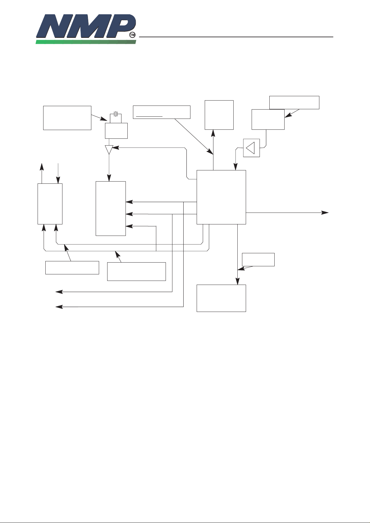
Clocking sceme
DSP Clock
60.2 MHz
differential sine
ear
AUDIO
CODEC
wave
mouth
oscillator
DSP
9712OJ
Technical Documentation
RFI Clock 13 MHz
Sleep Mode: 135.4kHz
enable
RFI
ASIC
8–8
Copyright Nokia Mobile Phones
RF System Clock
26 MHz
VCTCXO
SIMCLKSIMCLK
Codec Sync Clock
8 kHz
DBUSCLK 512kHz
DBUSSYNC 8kHz
All of the clock outputs can be disabled/enabled. DSP uses differential sinusoidal clock. DSP–clock buffer can be enabled/disabled.
Codec Main Clock and
data Transfer clock
512kHz
3.25 / 1.625
MHz
MCU Clock
26 MHz
MCU
Page 9
SYSTEM MODULE DS9
NHK–1
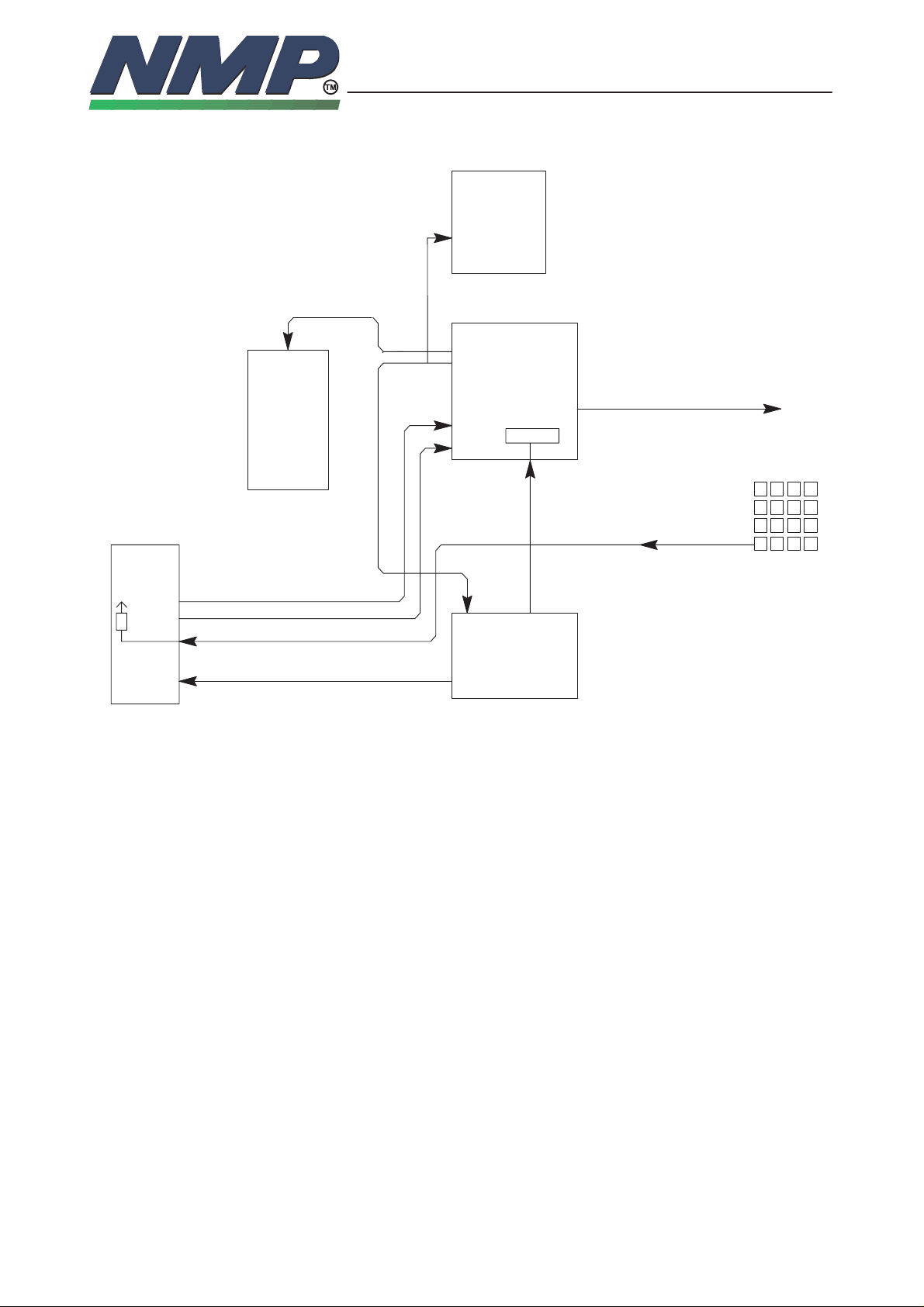
Reset and power control
reset in
DSP
9712OJ
Technical Documentation
RFI
Reset Out
Reset Out
ASIC
Vcc
Reset in
resetreg
8–9
Copyright Nokia Mobile Phones
SIMReset
PSL+
VL1
XRES reset in
XPWRON
XPwrOff
approx 2Hz
The supply power is switched on by PWR key on keyboard. All devices are
powered up at the same time by PSL+.
PSL+ supplies the reset to ASIC at power up. ASIC starts the clocks to DSP
and MCU. After some time ASIC releases the resets to all circuitry. Power up
reset resets MCU and RFI. DSP has own, independent reset from the asic.
For powering of the phone, the user pushes PWR–key. MCU detects that it is
pushed. After that the MCU cuts the eventual ongoing call, exits all tasks, acts
dead to the user and leaves PSL+ watchdog without resets. After power–down
delay PSL+ cuts the supply voltage from all the circuitry.
XPWRON
MCU
Page 10
SYSTEM MODULE DS9
NHK–1
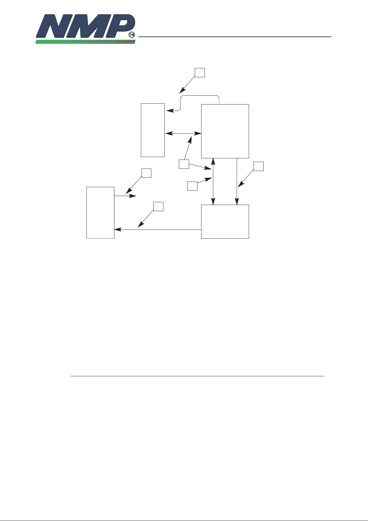
Watchdog system
XPWROFF
PSL
9712OJ
Technical Documentation
4
reset
DSP
1
5
2
POWER
3
8–10
Copyright Nokia Mobile Phones
ASIC
4
reset
MCU
Normal operation:
1. MCU tests DSP
2. MCU updates ASIC watchdog timer (> 2Hz)
3. MCU pulses the XPWROFF input on the PSL+ (about 2Hz)
Failed operation:
4. ASIC resets MCU and DSP (after about 0.5 sec failure)
5. PSL+ switches the power off (after 1.5 sec failure)
Names of functional blocks
Name: Function:
CTRLU Control unit for the phone
PWRU Power supply
DSPU Digital signal processing block
AUDIO Audio coding
ASIC EDSA –asic
RFI RF –baseband interface
Page 11

SYSTEM MODULE DS9
NHK–1
CTRLU
9712OJ
Technical Documentation
Copyright Nokia Mobile Phones
8–11
The control block provides a microcomputer unit (MCU) and it’s environment.
The environment consists of three memory circuits (FLASH, SRAM, EEPROM),
20 bit address bus and 8 bit data bus.
Main Features of the CTRLU block:
MCU functions:
– system control
– communication control
– user interface
– authentication
– RF monitoring
– power up/down control
– accessory monitoring
– batttery monitoring and charging control
– self–test and production testing
– flash loading
Main components of CTRLU
– Hitachi H8/536
H8/536 is a CMOS microcomputer unit (MCU) comprising a CPU
core and on–chip supporting modules with 16 bit architecture. The
data bus to outside world has 8 bits.
– 512 k x 8 bit FLASH memory
– 100 ns maximum read access time.
– contains the main program code for the MCU; part of the DSP
program code locates also in FLASH.
– In teh product two 256 k x 8 bit FLASH memories will be used
ASIC can address also two 4 Mbit or one 8 Mbit memories.
– 32 k x 8 bit SRAM memory
– 100 ns maximum read access time.
– 8 k x 8 bit EEPROM memory
– 150 ns maximum read access time.
– contains user defined information.
Page 12

SYSTEM MODULE DS9
NHK–1
Input signals of CTRLU
Name(from): Description:
VL1(PWRU) Power supply voltage for CTRLU block
VREF(PWRU) Reference voltage for MCU A/D converter
VBATDET(PWRU) Battery voltage detection
VC(PWRU) Charger voltage monitoring
EROMSELX(ASIC) Chip select for the EEPROM memory
ROMSELX(ASIC) Chip select for the FLASH memory
ROM2SELX(ASIC) Chip select for the 2nd FLASH memory
RAMSELX(ASIC) Chip select for the SRAM memory
RESETX(ASIC) Reset signal for MCU
NMI(ASIC) Non–maskable interrupt request
MCUCLK(ASIC) Main clock for MCU
9712OJ
Technical Documentation
8–12
Copyright Nokia Mobile Phones
IRQX(ASIC) Interrup request
PCMCDO(AUDIO) Audio codec control data receiving
TRF(RF) RF module temperature detection
VF(syst.conn.) Programming voltage for FLASH memory
RXD2_HOOK The use of handsfree monitoring
(syst.conn.) FLASH programming data input on the production line
TBAT(batt.conn.) Battery temperature detection
BTYPE(batt.conn.) Battery size identification
JCON(syst.conn.) Junction box connection identification
Output signals of CTRLU
Name(to): Description:
XPWROFF(PWRU) Power off control, PSL+ watchdog reset
PWM(PWRU) Charger on/off control
WSTROBEX(ASIC) MCU write strobe
RSTROBEX(ASIC) MCU read strobe
MCUAD(19:0)(ASIC)20 bit MCU address bus
MBUSDET(ASIC) MBUS activity detection
PCMCLK(AUDIO) Clock for audio cedec control data transfer
PCMCDI(AUDIO) Audio codec control data transmitting
XSELPCMC(AUDIO)Chip select for audio codec
Page 13

SYSTEM MODULE DS9
NHK–1
TXD2_PHFS Power on/off control for HF device, verification output
(syst.connector) of the programmed data of FLASH during programming
CALL_LED(UIF) Call ’coming’ indicator light control
BACKLIGHT(UIF) LCD and display backlight on/off control
BUZZER(UIF) Buzzer signal
Bidirectional signals of CTRLU
Name(to/from): Description:
MCUDA(7;0)(ASIC) MCU’s 8 bit data bus
M2BUS Asyncronous serial data bus
Block description of CTRLU
– MCU – memories
MCU has a 20 bits wide address bus A(19:0) and an 8–bit data bus
with memories. The address bits A(19:16) are used for chip select
decoding. The decoding is done in EDSA–asic.
9712OJ
Technical Documentation
8–13
Copyright Nokia Mobile Phones
On the Hitachi HD647536 internal memory map there is the following:
• 00000 – 0F67F 62k bytes internal ROM
• 0F680 – 0FE7F 2k bytes internal RAM
• 0FE80 – 0FFFF 384 bytes registers
External memory map is the following:
• 10000 – 17FFF 32k bytes RAM
• 20000 – 21FFF 8k bytes E
• 30000 – 300FF 256 bytes ASIC
• 40000 – 7FFFF 256k bytes FlashROM
• 80000 – BFFFF 256k bytes FlashROM
– CTRLU – PWRU
MCU controls the watchdog timer in PSL+. It sends a positive pulse
at approximately 2 Hz to XPWROFF pin of the PSL+ to keep the
power on. If MCU fails to deliver this pulse, the PSL+ will remove
power from the system. MCU controls also the charger on/off switching in the PWRU block. When power off is requested MCU leaves
PSL+ watchdog without reset. After the watchdog has elapsed PSL+
cuts off the supply voltages from the phone.
2
PROM
Page 14

SYSTEM MODULE DS9
NHK–1
– CTRLU – ASIC
MCU and ASIC have a common 8 bit data bus and a 9 bit address
bus. A(4:0) are used for normal addressing whereas bits A(19:16)
are decoded in ASIC to chip select inputs for CTRLU memories.
ASIC controls the main clock, main reset and interrupts to MCU. The
internal clock of MCU is half the MCUCLK clock speed. RESETX resets everything in MCU except the contents of the RAM. IRQX is
general purpose interrupt request line from ASIC. After IRQX request
the interrupt register of asic is read to find out the reason for interrupt. NMI–interrupt is used only to wake up MCU from software
standby mode.
– CTRLU – DSPU
MCU and DSP communicate through ASIC. ASIC has MCU–mailbox
and DSP–mailbox. MCU writes data to DSP–mailbox where DSP can
only read the incoming data. In MCU–mailbox data transfer direction
is opposite.
– CTRLU – AUDIO
9712OJ
Technical Documentation
8–14
Copyright Nokia Mobile Phones
When the the chip select signal XSELPCMC goes low, MCU writes
or reads control data to or from the speech codec at the rate defined
by PCMCLK. PCMCDI is output data line from MCU to codec and
PCMCDO is input data line from codec to MCU.
– CTRLU – RF/BATTERY monitoring
MCU monitors RF and battery functions (BTEMP, BSI ,VBATDET,VC
and TRF) with the internal 8 channel 10 bit AD converter.
– CTRLU – keyboard and LCD driver interface
MCU and user interface communication is controlled through ASIC.
– CTRLU – ACCESSORIES
M2BUS is used to control external accessories. This interface can be
used also to factory testing and service and maintenance purposes.
Page 15

SYSTEM MODULE DS9
NHK–1
PWRU
The power block makes the supply voltages for the baseband and includes also
the charging electronics.
Main components of PWRU
– PSL + ASIC
Generates the voltages, has power switch, charger and battery
detection and watchdog.
– Transistor BCP69–25 and schottky STPS340U
The charging current is passed through these components.
– Transistor BCX51
VL regulators of PSL+ external output transistors.
Input signals of PWRU
Name(from): Description:
9712OJ
Technical Documentation
8–15
Copyright Nokia Mobile Phones
XPWRON(UIF) PWR on swith
XPWROFF(CTRLU) Power off control
VBATT(syst.conn.) Battery voltage
PWM(CTRLU) Charger on/off control
VCHAR(syst.conn.) Charging voltage
Output signals of PWRU
Name(from): Description:
XRES(ASIC) Master reset
VL1(CTRLU,ASIC, Logic supply voltage, max 150 mA
RFI,UIF)
VL2(DSPU) Logic supply voltage, max 150 mA
VA1(AUDIO,UIF) Analog supply voltage, max 40 mA
VA2(RFI) Analog supply voltage, max 80 mA
Page 16

SYSTEM MODULE DS9
NHK–1
Block description of PWRU
The PSL+–IC produces the supply voltages:
Name: Description:
2 * VL 150 mA for logic
VA1 40 mA for audios
VA2 80 mA for RFI
VREF 5 mA reference
It also has internal watchdog, voltage detection and charger detection func-
tions. The watchdog will cut the output voltages if it is not resetted once in
about 0.7 seconds. The voltage detector resets the phone if the battery voltage
falls below 4.8 V (±0.2 V). The charger detection starts the phone if it is in power–off when the charging voltage is applied.
The charging electronics is controlled by the MCU. When the charging voltage
is applied to the phone while the phone is powered up, the MCU detects it and
starts controlling the charging.
9712OJ
Technical Documentation
8–16
Copyright Nokia Mobile Phones
If the phone is in power–off state, the PSL+ will detect the charging voltage and
start the phone. If the battery voltage is high enough the reset will be released
and the MCU will start controlling the charging.
If the battery voltage is too low the phone is in reset and charging control circuitry will pass the charging current to the battery. When the battery voltage has
reached 5.25 V (±0.2 V) the reset will be removed and the MCU starts controlling the charging. This all is invisible to the user.
Page 17

SYSTEM MODULE DS9
NHK–1
DSPU
9712OJ
Technical Documentation
Copyright Nokia Mobile Phones
Main interfaces of the DSP:
– MCU via ASIC mailbox
– ASIC
– audio codec
– data bus interface (DBUS) for accessories
– digital audio interface (DAI) for type approval measurements
Main features of the DSP block:
– speech processing
– speech coding/decoding
– RPE–LTP–LPC (Regular pulse excitation long term
prediction linear predictive coding)
– voice activity detection (VAD) for discontinuous transmission
(DTX)
8–17
– comfort noise generation during silence
– acoustic echo cancellation
– channel coding and transmission
– block coding (with ASIC)
– convolutional coding
– interleaving
– ciphering (with ASIC)
– burst building and writing it to ASIC
– Reception
– reading the A/D conversion results from ASIC
– impulse response calculation
– matched filtering
– bit detection (with Viterbi on ASIC)
– deinterleaving of soft decisions
– convolutional decoding (with Viterbi)
– block decoding (with ASIC)
– Adjacent cell monitoring
– signal strenght measurements
– neighbour timing measurements
– neighbour parameter reception
Page 18

SYSTEM MODULE DS9
NHK–1
– control functions
– RF controls
– frame structure control
ASIC)
– test functions
– functions for RF measurements
– debugging functions for product development
9712OJ
Technical Documentation
Copyright Nokia Mobile Phones
– synthesizer control
– power ramp programming
– automatic gain control (AGC)
– automatic frequency control (AFC)
– controlling the operations during a TDMA frame (with
– controlling the multiframe structure
– channel configuration control
8–18
Main components of DSPU
– AT&T DSP 1616
– SRAMs for DSP external memory
Input signals of DSPU
Name(from): Description:
VL2(PWRU) Logic supply voltage, max 150 mA
DSPCLKEN(ASIC) Clock enable for DSP clock oscillator circuit
DSP1RSTX(ASIC) Reset for the DSP
PCMDATRCLKX PCM data input clock
(ASIC) DBUS data output clock
CODEC_CLK PCM data output clock
PCMOUT(AUDIO) Received audio in PCM format
DBUSCLK DBUS data output clock
DBUSSYNC DBUS data bit sync clock
RDA DBUS received data
INT0, INT1(ASIC) Interrupts for the DSP
PCMCOSYCLKX PCM data bit sync clock
(ASIC)
Page 19

SYSTEM MODULE DS9
NHK–1
Output signals of DSPU
Name(to): Description:
PCMIN(AUDIO) Transmitted audio in PCM format
IOX(ASIC) I/O enable, indicates access to DSP address space
RWX(ASIC) Read/write X
DSPAD(16;9)(ASIC) Address bus and control signals
DBUSDET(ASIC) DBUS activity detection
Bidirectional signals of DSPU
Name(from/to): Description:
DSPDA(15;0)(ASIC) 16 bit data bus
Block description of DSPU
Control unit communicates with DSP circuitry trough a mailbox in the ESA asic.
DSP communicates with PCM codec and DBUS with SIO serial busses. DSP
controls RFI through the ESA.
9712OJ
Technical Documentation
8–19
Copyright Nokia Mobile Phones
In transmit mode DSP codes the speech and routes the resulting transmit slots
to ESA. ESA asic controls timing, and at specified intervals sends these bits to
RFI for DA conversion.
In digital receive mode RFI AD converts IF signal from RF unit under the control of ESA. DSP controls ESA and receives the converted bits. After channel
and speech decoding, bits are converted to an analog signal in the PCM codec,
routed and fed to the earpiece.
DSP controls RF trough the ESA asic, where all necessary timing functions are
implemented, and control IO lines are provided for eg. synte loading.
All clocks and timing are generated from the RFC clock.
DSP emulator can be connected to DSP pins TCK,TMS,TDO,TDI,GND and
VDD.
Page 20

SYSTEM MODULE DS9
NHK–1
AUDIO
The block consists of audio codec with some peripheral components. The codec includes microphone and earpiece amplifier and all the necessary switches
for routing. The controlling of the codec is done by the MCU. The PCM data
comes from and goes to DSP.
Main components of AUDIO
– Audio codec ST5080
Includes e.g. PCM codec, audio routing switches, microphone and
earpiece amplifiers for 2 connections (internal and external devices)
and DTMF generator.
Input signals of AUDIO
Name(from): Description:
VA1(PWRU) Analog supply voltagee, max 40 mA
PCMIN(DSPU) Received audio in PCM format
9712OJ
Technical Documentation
8–20
Copyright Nokia Mobile Phones
SYNC(ASIC) 8 kHz frame sync
CODEC_CLK(ASIC) 512 kHz codec main clock
PCMCDI(CTRLU) Audio codec control data
PCMCLK(CTRLU) Clock for audio codec control data transfer
XSELPCMC Audio codec chip select
(CTRLU)
HFMIC(syst.conn.) External microphone
MICN,MICP(UIF) Differential microphone signal
Output signals of AUDIO
Name(to): Description:
PCMOUT(DSPU) Transmitted audio in PCM format
PCMCDO(CTRLU) Audio codec control data
MIC_EN(UIF) Microphone enable
EXTEAR(syst.conn.) External received audio
EARN,EARP(UIF) Internal received audio
JCONN(CTRLU) Junction box connected signal (multiplexed with HFMIC)
Block description of AUDIO
The audio codec communicates with the DSP (analog speech) through a SIO
(signals: PCMIN, SYNC, CODEC_CLK and PCMOUT) . MCU controls the audio codec functionality through a separate SIO (signals: PCMCDO, PCMCDI,
PCMCLK and XSELPCMC).
Page 21

SYSTEM MODULE DS9
NHK–1
ASIC
The ASIC takes care of the following functions:
– interface between MCU and UIF
– interface between MCU, DSP and RFI
– hardware accelerator functions to DSP: Viterbi, ...
– clock generation and disable/enable
– RF–controls
– UIF–interface
– timers
– M2BUS interface
– SIM interface
Main components of ASIC
– ESA –ASIC
9712OJ
Technical Documentation
8–21
Copyright Nokia Mobile Phones
– RFC –buffer
Input signals of ASIC
Name(from): Description:
VL1(PWRU) Logic supply voltage ax 150 mA
IOX(DSPU) I/O enable, indicates access to DSP address space
RWX(DSPU) Read/write X
WSTROBEX MCU’s write strobe
(CTRLU)
RSTROBEX MCU’s read strobe
(CTRLU)
RFC(RF) Reference clock from VCTCXO
XRES(PWRU) Master reset
DSPAD(16;0)(DSPU)Address bus and control signals
MCUAD(19;16,4;0) MCU’s address bus
(CTRLU)
Inverter buffer stage is used as a buffer for VCTCXO–clock.
DAX(RFI) Data acknowledge
MBUSDET(CTRLU) MBUS activity detection
DBUSDET(DSPU) DBUS activity detection
Page 22

SYSTEM MODULE DS9
NHK–1
Output signals of ASIC
Name(to): Description:
INT0,INT1(DSPU) Interrupts for DSP
NMI(CTRLU) Not maskable interrup request
IRQX(CTRLU) Interrupt request
RESETX Master (power up) reset
(CTRLU,RFI)
DSP1RSTX(DSPU) Reset for the DSP
SIMRESET Reset for the SIM
WRX(RFI) Write strobe
RDX(RFI) Read strobe
RFIAD(3;0)(RFI) RFI address bus
SCLK(RF) Synthesizer load clock
9712OJ
Technical Documentation
8–22
Copyright Nokia Mobile Phones
SDATA(RF) Synthesizer load data
SENAR(RF) Receiver synthesizer enable
SENAT(RF) Transmit synthesizer enable
RXPWR(RF) RX circuitry power enable
TXPWR(RF) TX circuitry power enable
SYNTHPWR(RF) Synthesizer circuitry power enable
TXP(RF) Transmit enable
MCUCLK(CTRLU) Main clock for MCU
DSPCLKEN(DSPU) DSP clock circuit enable
RFICLK(RFI) RFI master clock
RFI2CLK(RFI) RFI sleep clock
CODEC_CLK PCM data clock
(DSPU,AUDIO)
PCMDATRCLKX Inverted PCM data clock, used as input clock for
(DSPU) codec and DBUS interface
SYNC(AUDIO) Bit sync clock
PCMCOSYCLKX Bit sync clock, inverted
(DSPU)
DCLK(DSPU) DBUS data clock
DSYNC(DSPU) DBUS bit sync clock
SIMCLK(UIF) SIM data clock
VSIM(UIF) SIM power control
Page 23

SYSTEM MODULE DS9
NHK–1
ROMSELX(CTRLU) Chip select for the FLASH memory
ROM2SELX Chip select for the second FLASH memory
(CTRLU)
EROMSELX Chip select for the EEPROM memory
(CTRLU)
RAMSELX(CTRLU) Chip select for the SRAM memory
COL(3;0)(UIF) Lines for keyboard column write
Bidirectional signals of ASIC
Name(from/to): Description:
DSPDA(15;0) 16 bit data bus
(DSPU)
MCUDA(7;0) MCU’s 8 bit data bus
(CTRLU)
RFIDA(11;0)(RFI) 12 bit data bus
9712OJ
Technical Documentation
8–23
Copyright Nokia Mobile Phones
UIF(6;0)(UIF) LCD controller control and keyboard read bus
SIMDATA(UIF) Serial data to SIM
Block description of ASIC
RFC buffer buffers the 26 MHz clock from VCTCXO to ASIC. In ASIC that clock
is further buffered and divided for MCU, RFI and audio codec (main and sync
clocks). The clock outputs can be disabled in order to save current when the
clock is not needed. Also DSP oscillator can be stopped.
Page 24

SYSTEM MODULE DS9
NHK–1
RFI
The block consists of RFI–ASIC and its reference voltage generator. This block
is an interface between RF and baseband. The block has the following functions:
– IF receiving and A/D conversion
– I/Q separation
– I and Q transmit and D/A conversion
– AFC D/A
– TXC
– digital AGC control through PDATA
The RFI is connected to ESA with a 12–bit databus. The registers in RFI are
accessed using 4 address bits.
Main components of RFI
– RFI –ASIC
9712OJ
Technical Documentation
8–24
Copyright Nokia Mobile Phones
– 4.096 V external voltage reference LM4040 for RFI
Input signals of RFI
Name(from): Description:
VL1(PWRU) Logic supply voltage, max 150 mA
VA2(PWRU) Analog supply voltage, max 80 mA
RESETX(PWRU) Master (power up) reset
RFIAD(3;0)(ASIC) RFI address bus
RDX(ASIC) Read strobe
WRX(ASIC) Write strobe
RFICLK(ASIC) RFI master clock
RFI2CLK(ASIC) RFI sleep clock
Page 25

SYSTEM MODULE DS9
NHK–1
Output signals of RFI
Name(to): Description:
DAX(ASIC) Data acknowledge
AFC(RF) Automatic frequency control voltage
TXC(RF) TX transmit power control voltage
TXQP,TXQN(RF) Differential TX quadrature signal
TXIP,TXIN(RF) Differential TX inphase signal
PDATA(5;0)(RF) Parallel AGC data
RXQ(RF) RX quadrature signal
RXI(RF) RX inphase signal
Bidiractional signals of RFI
Name(to): Description:
9712OJ
Technical Documentation
8–25
Copyright Nokia Mobile Phones
RFIDA(11;0)(ASIC) 12 bit data bus
Page 26

SYSTEM MODULE DS9
NHK–1
RF block
The RF block carries out all the RF functions of the transceiver. The RF block
works in PCN (DCS11800) system.
Functional description
Regulators
There are two regulators in the RF unit. The 1st regulator is used for the synthesizers and the negative bias generator. The 2nd regulator is used for te other RF circuits. The regulators regulate the battery voltage to the fixed 4.75 V
level. The receiver, synthesizer and transmitter circuits can be switched ON and
OFF separately. Switching sequence timing depends on the operation mode of
the phone.
Power distribution
All currents in power distribution diagram are peak currents. Activity percentages are in SPEECH mode 22.5 % for RXPWR , 15.8 % for TXPWR and 100 %
for SYNTHPWR. In IDLE mode activities are 0.36 %, 0.0 % and 1.61 % respectively. The current of each block is controlled independently and for example
TXPWR and RXPWR are not on at the same time. Average current consumption in SPEECH mode is 340 mA and in IDLE mode 22 mA for whole tranceiver.
9712OJ
Technical Documentation
8–26
Copyright Nokia Mobile Phones
Battery
6.0 V
Regulator Regulator
4.75 V4.75 V
45 mA 5 mA 60 mA 60 mA
UHF PLL
VHF PLL
Buffers
Negat. bias
generator
RF LNAs
IF amplifiers
Mixers
AGC amplifiers
Modulator
TX buffers
Power control
VCTCXO
Switch
Power
amplifier
2 mA
850 mA
VREF
SYNTHPWR
TXP
TXPWR
RXPWR
Page 27

SYSTEM MODULE DS9
NHK–1
Control signals
In the following table (NO TAG) the RF current consumption can be seen with
different status of the control signals. The VCTCXO current is not included in
the results.
SYNTHPWR:RXPWR: TXPWR: TXP: Typ. load current: Notes:
L L L L 0.05 mA Leakage current
H L L L 51 mA Synthesizer active
H H L L 110 mA Reception
H L H L 110 mA TX active
H L H H 960 mA Transmission
Receiver
The received RF signal from the antenna is fed via a duplex filter to the receiver
unit. The signal is amplified by a discrete low noise preamplifier. The gain of the
amplifier is controlled by the AGC control line (PDATA0). The nominal gain of
10 dB is reduced in the strong field condition about 28 dB. After the preamplifier the signal is filtered by a three pole ceramic RF filter. The filter rejects spurious signals coming from the antenna and spurious emissions coming from the
receiver unit.
9712OJ
Technical Documentation
8–27
Copyright Nokia Mobile Phones
The filtered signal is amplified by a transistor amplifier and down converted by
a passive diode mixer. The frequency of the first IF is 487 MHz. The first local
signal is generated by the UHF synthesizer. The IF signal is amplified and then
it is filtered by a microstripline filter. The filter has a differential output.
The filtered IF signal is fed to the receiver integrated circuit, PMB2403S. The
circuit down converts the first IF signal. The 2nd local signal is generated by the
VHF synthesizer. The frequency of the second IF is 87 MHz. The 2ndIF signal
is filtered by a SAW filter. The filter rejects adjacent channel signal, intermodulating signals and the 3rd IF image signal. After filtering the 2nd IF signal is amplified by a AGC amplifier. The AGC amplifier is a separate IC and the gain
control range is 45 dB. The gain is controlled digitally with four control lines.
The 2nd IF signal is fed back to the receiver IC (PMB3403S), which has one 12
dB AGC stage. The amplified IF signal is down converted in the 2nd mixer of
the IC. The 3rd local signal is generated from VHF VCO by dividing the original
VCO signal by four. The 3rd intermediate frequency is 13 MHz. After the downconversion the 3rd IF signal is amplified and fed out from the RX IC.
The 3rd IF signal is filtered by a ceramic filter. The filter rejects signals of the
adjacent channels. After the filtering the signal is amplified and divided into the I
and Q signals by an RC network. The I and Q signal are fed to the RFI interface IC.
Page 28

SYSTEM MODULE DS9
NHK–1
Transmitter
The TX intermediate frequency of 400 MHz is modulated by an I/Q modulator
(PMB2205S). The TX I and Q signals are generated in the RFI interface circuit
and they are fed differentially to the modulator.
The final TX signal ia achieved by mixing the UHF VCO signal and the modulated TX intermediate signal. After mixing the TX signal is amplified and filtered
by two amplifiers and filters. After these stages the level of the sinal is typically
1 mW (0 dBm).
The power amplifier module amplifies the TX signal to the desired power level.
The maximum output level of the module is typically 2.0 W.
The power control loop controls the output level of the power amplifier. The
power detector consists of a directional coupler and a diode rectifier. The power
control signal (TXC), which has a raised cosine form, comes from the RF interface circuit, RFI.
Frequency synthesizers
9712OJ
Technical Documentation
8–28
Copyright Nokia Mobile Phones
The stable frequency source for the synthesizers and base band circuits is the
voltage controlled temperature compensated crystal oscillator, VCTCXO. The
frequency of the VCTCXO is 26 MHz. The frequency of the oscillator is controlled by an AFC voltage, which is generated by the base band circuits.
The operating frequency range of the UHF synthesizer is from 1318 to 1393
MHz in the receiving mode and from 1310 to 1385 MHz in the transmitting
mode. The UHF VCO is a module. The dual modulus divider divides the VCO
signal by 32/33 for the PLL circuit (PMB2306). The UHF PLL generates the
down conversion signal for the receiver and the up conversion signal for the
transmitter.
The operating frequency of the VHF synthesizer is 400 MHz. This signal is directly used in the 2nd mixer of the receiver and in the I/Q modulator of the
transmitter chain. The VHF signal is divided by four, too. This signal is used in
the 3rd mixer of the receiver and in the PLL circuit.
Page 29

SYSTEM MODULE DS9
NHK–1
9712OJ
Technical Documentation
Block diagram of baseband
32K x 16
SRAM
ear
PCM
CODEC
mic
sio
DAI
A14:0,
D15:0
sio
DSP
ext
sio
mem
A5:0,
D15:0
RFI
12 bit parallel +
8 x control
ASIC
8–29
Copyright Nokia Mobile Phones
RF
UIF–module
LCD
DRIVER
LCD
LCD
PSL+
CHRGR
FLASH
LOAD
M2 BUS
Interface
A4:0, A19:16, D7:0
A19:0,D7:0
io ext mem
io
sio
sio
MCU
sio
A12:0,D7:0
E2PROM
8K X 8
A17:0,D7:0
512K x 8
FLASH
A14:0,D7:0
32K x 8
SRAM
Page 30

487 MHZ
87 MHZ
4
AGC
AMPLIFIER
PMB2403S V1.3
13 MHZ
6
AGC CONT.
RXI
RXQ
Block diagram of RF
SYSTEM MODULE DS9
9712OJ
Technical Documentation
SWITCH
EXT . ANTENNA
POWER
CONTROL
1310...1393 MHZ
UHF
VCO
DIV
32/33
PMB2306
UHF
PLL
400 MHZ
VHF
VCO
MODULATOR
DIV
4
PMB2205S
I/Q
PMB2306
VHF
PLL
PLL
REGUL.
RF
REGUL.
VCTCXO
26 MHZ
3
4
2
2
2
DC CONT.
AFC
SYS.CLOCK
PLL CONT.
TX CONT.
TXI
TXQ
Copyright Nokia Mobile Phones
NHK–1
8–30
Page 31

SYSTEM MODULE DS9
NHK–1
9712OJ
Technical Documentation
Power distribution diagram
PSL+
VBATT
VCHAR
VL1
VL2
VA1
VA2
VREF
VA2 VL1
RFI
8–31
Copyright Nokia Mobile Phones
VBATT VREF
RF
VL2
32Kx16
SRAM
VA1
PCM
CODEC
DSP
VL2
VL1
ASIC
VREF VL1
MCU
MCU
VA1
VL1
VL1
E2PROM
8K x 8
UIF–module
UIF–module
LCD Driver
VL1
512K x 8
FLASH
VBATT
LCD
LCD
VL1
32K x 8
SRAM
Page 32

SYSTEM MODULE DS9
NHK–1
9712OJ
Technical Documentation
Copyright Nokia Mobile Phones
Connections between system and RF blocks
8–32
Page 33

SYSTEM MODULE DS9
NHK–1
9712OJ
Technical Documentation
Copyright Nokia Mobile Phones
Parts list of DS9 v.1.20 code 0200172
ITEM CODE DESCRIPTION VALUE TYPE
R070 1430788 Chip resistor 22 k 5 % 0.063 W 0402
R071 1430794 Chip resistor 39 k 5 % 0.063 W 0402
R072 1430754 Chip resistor 1.0 k 5 % 0.063 W 0402
R073 1430764 Chip resistor 3.3 k 5 % 0.063 W 0402
R074 1430730 Chip resistor 150 5 % 0.063 W 0402
R075 1430804 Chip resistor 100 k 5 % 0.063 W 0402
R076 1430744 Chip resistor 470 5 % 0.063 W 0402
R077 1430796 Chip resistor 47 k 5 % 0.063 W 0402
R078 1430796 Chip resistor 47 k 5 % 0.063 W 0402
R079 1430804 Chip resistor 100 k 5 % 0.063 W 0402
R110 1430842 Chip resistor 680 k 1 % 0.063 W 0402
R111 1430840 Chip resistor 220 k 1 % 0.063 W 0402
R112 1430804 Chip resistor 100 k 5 % 0.063 W 0402
R113 1430804 Chip resistor 100 k 5 % 0.063 W 0402
R114 1430732 Chip resistor 180 5 % 0.063 W 0402
R140 1430792 Chip resistor 33 k 5 % 0.063 W 0402
R141 1430788 Chip resistor 22 k 5 % 0.063 W 0402
R142 1430778 Chip resistor 10 k 5 % 0.063 W 0402
R143 1430764 Chip resistor 3.3 k 5 % 0.063 W 0402
R144 1430764 Chip resistor 3.3 k 5 % 0.063 W 0402
R145 1430732 Chip resistor 180 5 % 0.063 W 0402
R146 1430846 Chip resistor 2.7 k 1 % 0.063 W 0402
R147 1430844 Chip resistor 3.9 k 1 % 0.063 W 0402
R148 1430762 Chip resistor 2.2 k 5 % 0.063 W 0402
R149 1430762 Chip resistor 2.2 k 5 % 0.063 W 0402
R150 1430778 Chip resistor 10 k 5 % 0.063 W 0402
R151 1430804 Chip resistor 100 k 5 % 0.063 W 0402
R152 1430778 Chip resistor 10 k 5 % 0.063 W 0402
R160 1430726 Chip resistor 100 5 % 0.063 W 0402
R161 1430770 Chip resistor 4.7 k 5 % 0.063 W 0402
R162 1430778 Chip resistor 10 k 5 % 0.063 W 0402
R163 1430726 Chip resistor 100 5 % 0.063 W 0402
R164 1430788 Chip resistor 22 k 5 % 0.063 W 0402
R165 1430804 Chip resistor 100 k 5 % 0.063 W 0402
R166 1430804 Chip resistor 100 k 5 % 0.063 W 0402
R169 1430804 Chip resistor 100 k 5 % 0.063 W 0402
R170 1430804 Chip resistor 100 k 5 % 0.063 W 0402
R171 1430788 Chip resistor 22 k 5 % 0.063 W 0402
R172 1430796 Chip resistor 47 k 5 % 0.063 W 0402
R173 1430796 Chip resistor 47 k 5 % 0.063 W 0402
R174 1430754 Chip resistor 1.0 k 5 % 0.063 W 0402
R175 1430700 Chip resistor 10 5 % 0.063 W 0402
R176 1430726 Chip resistor 100 5 % 0.063 W 0402
8–33
Page 34

SYSTEM MODULE DS9
NHK–1
9712OJ
Technical Documentation
R177 1430726 Chip resistor 100 5 % 0.063 W 0402
R178 1430726 Chip resistor 100 5 % 0.063 W 0402
R179 1430726 Chip resistor 100 5 % 0.063 W 0402
R181 1430726 Chip resistor 100 5 % 0.063 W 0402
R182 1430726 Chip resistor 100 5 % 0.063 W 0402
R183 1430734 Chip resistor 220 5 % 0.063 W 0402
R184 1430726 Chip resistor 100 5 % 0.063 W 0402
R185 1430726 Chip resistor 100 5 % 0.063 W 0402
R186 1430726 Chip resistor 100 5 % 0.063 W 0402
R190 1430726 Chip resistor 100 5 % 0.063 W 0402
R191 1430754 Chip resistor 1.0 k 5 % 0.063 W 0402
R192 1430754 Chip resistor 1.0 k 5 % 0.063 W 0402
R193 1430754 Chip resistor 1.0 k 5 % 0.063 W 0402
R194 1430754 Chip resistor 1.0 k 5 % 0.063 W 0402
R195 1430754 Chip resistor 1.0 k 5 % 0.063 W 0402
R196 1430754 Chip resistor 1.0 k 5 % 0.063 W 0402
R197 1430754 Chip resistor 1.0 k 5 % 0.063 W 0402
R198 1430804 Chip resistor 100 k 5 % 0.063 W 0402
R199 1430804 Chip resistor 100 k 5 % 0.063 W 0402
R210 1430754 Chip resistor 1.0 k 5 % 0.063 W 0402
R230 1430804 Chip resistor 100 k 5 % 0.063 W 0402
R231 1430804 Chip resistor 100 k 5 % 0.063 W 0402
R232 1430842 Chip resistor 680 k 1 % 0.063 W 0402
R233 1430796 Chip resistor 47 k 5 % 0.063 W 0402
R234 1430778 Chip resistor 10 k 5 % 0.063 W 0402
R235 1430762 Chip resistor 2.2 k 5 % 0.063 W 0402
R236 1430762 Chip resistor 2.2 k 5 % 0.063 W 0402
R237 1430762 Chip resistor 2.2 k 5 % 0.063 W 0402
R238 1430762 Chip resistor 2.2 k 5 % 0.063 W 0402
R239 1430762 Chip resistor 2.2 k 5 % 0.063 W 0402
R240 1430762 Chip resistor 2.2 k 5 % 0.063 W 0402
R241 1430762 Chip resistor 2.2 k 5 % 0.063 W 0402
R243 1430774 Chip resistor 6.8 k 5 % 0.063 W 0402
R244 1430804 Chip resistor 100 k 5 % 0.063 W 0402
R245 1430804 Chip resistor 100 k 5 % 0.063 W 0402
R246 1430804 Chip resistor 100 k 5 % 0.063 W 0402
R247 1430762 Chip resistor 2.2 k 5 % 0.063 W 0402
R248 1430726 Chip resistor 100 5 % 0.063 W 0402
R249 1430726 Chip resistor 100 5 % 0.063 W 0402
R250 1430804 Chip resistor 100 k 5 % 0.063 W 0402
R251 1430792 Chip resistor 33 k 5 % 0.063 W 0402
R252 1430804 Chip resistor 100 k 5 % 0.063 W 0402
R253 1430770 Chip resistor 4.7 k 5 % 0.063 W 0402
R254 1430760 Chip resistor 1.8 k 5 % 0.063 W 0402
R255 1430726 Chip resistor 100 5 % 0.063 W 0402
R256 1430726 Chip resistor 100 5 % 0.063 W 0402
R257 1430726 Chip resistor 100 5 % 0.063 W 0402
R260 1430726 Chip resistor 100 5 % 0.063 W 0402
Copyright Nokia Mobile Phones
8–34
Page 35

SYSTEM MODULE DS9
NHK–1
9712OJ
Technical Documentation
R261 1430784 Chip resistor 15 k 5 % 0.063 W 0402
R262 1430804 Chip resistor 100 k 5 % 0.063 W 0402
R263 1430760 Chip resistor 1.8 k 5 % 0.063 W 0402
R264 1430792 Chip resistor 33 k 5 % 0.063 W 0402
R265 1430792 Chip resistor 33 k 5 % 0.063 W 0402
R267 1430778 Chip resistor 10 k 5 % 0.063 W 0402
R270 1430752 Chip resistor 820 5 % 0.063 W 0402
R502 1430770 Chip resistor 4.7 k 5 % 0.063 W 0402
R503 1430778 Chip resistor 10 k 5 % 0.063 W 0402
R504 1430772 Chip resistor 5.6 k 5 % 0.063 W 0402
R505 1430754 Chip resistor 1.0 k 5 % 0.063 W 0402
R506 1430734 Chip resistor 220 5 % 0.063 W 0402
R507 1430700 Chip resistor 10 5 % 0.063 W 0402
R508 1430700 Chip resistor 10 5 % 0.063 W 0402
R509 1430762 Chip resistor 2.2 k 5 % 0.063 W 0402
R510 1430700 Chip resistor 10 5 % 0.063 W 0402
R511 1430778 Chip resistor 10 k 5 % 0.063 W 0402
R512 1430726 Chip resistor 100 5 % 0.063 W 0402
R513 1430778 Chip resistor 10 k 5 % 0.063 W 0402
R514 1430714 Chip resistor 33 5 % 0.063 W 0402
R516 1430764 Chip resistor 3.3 k 5 % 0.063 W 0402
R517 1430720 Chip resistor 56 5 % 0.063 W 0402
R518 1430740 Chip resistor 330 5 % 0.063 W 0402
R519 1430700 Chip resistor 10 5 % 0.063 W 0402
R520 1430740 Chip resistor 330 5 % 0.063 W 0402
R521 1430764 Chip resistor 3.3 k 5 % 0.063 W 0402
R522 1430200 Chip resistor 120 2 % 0.063 W 0603
R526 1430200 Chip resistor 120 2 % 0.063 W 0603
R527 1430796 Chip resistor 47 k 5 % 0.063 W 0402
R528 1430796 Chip resistor 47 k 5 % 0.063 W 0402
R529 1430796 Chip resistor 47 k 5 % 0.063 W 0402
R530 1430796 Chip resistor 47 k 5 % 0.063 W 0402
R531 1430796 Chip resistor 47 k 5 % 0.063 W 0402
R533 1430734 Chip resistor 220 5 % 0.063 W 0402
R534 1430748 Chip resistor 680 5 % 0.063 W 0402
R535 1430734 Chip resistor 220 5 % 0.063 W 0402
R536 1430748 Chip resistor 680 5 % 0.063 W 0402
R537 1430764 Chip resistor 3.3 k 5 % 0.063 W 0402
R539 1430766 Chip resistor 3.9 k 5 % 0.063 W 0402
R540 1430770 Chip resistor 4.7 k 5 % 0.063 W 0402
R541 1430726 Chip resistor 100 5 % 0.063 W 0402
R542 1430774 Chip resistor 6.8 k 5 % 0.063 W 0402
R543 1430754 Chip resistor 1.0 k 5 % 0.063 W 0402
R544 1430770 Chip resistor 4.7 k 5 % 0.063 W 0402
R545 1430748 Chip resistor 680 5 % 0.063 W 0402
R546 1430748 Chip resistor 680 5 % 0.063 W 0402
R548 1430790 Chip resistor 27 k 5 % 0.063 W 0402
R560 1430732 Chip resistor 180 5 % 0.063 W 0402
Copyright Nokia Mobile Phones
8–35
Page 36

SYSTEM MODULE DS9
NHK–1
9712OJ
Technical Documentation
R561 1430764 Chip resistor 3.3 k 5 % 0.063 W 0402
R562 1430764 Chip resistor 3.3 k 5 % 0.063 W 0402
R563 1430764 Chip resistor 3.3 k 5 % 0.063 W 0402
R564 1430744 Chip resistor 470 5 % 0.063 W 0402
R565 1430754 Chip resistor 1.0 k 5 % 0.063 W 0402
R566 1800554 NTC resistor 4.7 k 10 % 0.12 W 0805
R567 1430740 Chip resistor 330 5 % 0.063 W 0402
R568 1430796 Chip resistor 47 k 5 % 0.063 W 0402
R569 1430734 Chip resistor 220 5 % 0.063 W 0402
R600 1430770 Chip resistor 4.7 k 5 % 0.063 W 0402
R601 1430770 Chip resistor 4.7 k 5 % 0.063 W 0402
R602 1430732 Chip resistor 180 5 % 0.063 W 0402
R604 1430770 Chip resistor 4.7 k 5 % 0.063 W 0402
R605 1430770 Chip resistor 4.7 k 5 % 0.063 W 0402
R606 1430710 Chip resistor 22 5 % 0.063 W 0402
R607 1430760 Chip resistor 1.8 k 5 % 0.063 W 0402
R608 1430754 Chip resistor 1.0 k 5 % 0.063 W 0402
R609 1430754 Chip resistor 1.0 k 5 % 0.063 W 0402
R610 1430754 Chip resistor 1.0 k 5 % 0.063 W 0402
R611 1430710 Chip resistor 22 5 % 0.063 W 0402
R612 1430774 Chip resistor 6.8 k 5 % 0.063 W 0402
R613 1430794 Chip resistor 39 k 5 % 0.063 W 0402
R614 1430700 Chip resistor 10 5 % 0.063 W 0402
R615 1430726 Chip resistor 100 5 % 0.063 W 0402
R616 1430720 Chip resistor 56 5 % 0.063 W 0402
R617 1430700 Chip resistor 10 5 % 0.063 W 0402
R618 1430832 Chip resistor 2.7 k 5 % 0.063 W 0402
R619 1430778 Chip resistor 10 k 5 % 0.063 W 0402
R620 1430726 Chip resistor 100 5 % 0.063 W 0402
R621 1430742 Chip resistor 390 5 % 0.063 W 0402
R700 1430700 Chip resistor 10 5 % 0.063 W 0402
R701 1430730 Chip resistor 150 5 % 0.063 W 0402
R702 1412286 Chip jumper 0805
R703 1430740 Chip resistor 330 5 % 0.063 W 0402
R704 1430760 Chip resistor 1.8 k 5 % 0.063 W 0402
R705 1430774 Chip resistor 6.8 k 5 % 0.063 W 0402
R706 1430778 Chip resistor 10 k 5 % 0.063 W 0402
R707 1430784 Chip resistor 15 k 5 % 0.063 W 0402
R709 1430790 Chip resistor 27 k 5 % 0.063 W 0402
R710 1430710 Chip resistor 22 5 % 0.063 W 0402
R711 1430760 Chip resistor 1.8 k 5 % 0.063 W 0402
R712 1430754 Chip resistor 1.0 k 5 % 0.063 W 0402
R713 1430754 Chip resistor 1.0 k 5 % 0.063 W 0402
R714 1430754 Chip resistor 1.0 k 5 % 0.063 W 0402
R715 1430794 Chip resistor 39 k 5 % 0.063 W 0402
R800 1430210 Chip resistor 7.5 k 2 % 0.063 W 0603
R801 1430210 Chip resistor 7.5 k 2 % 0.063 W 0603
R802 1430210 Chip resistor 7.5 k 2 % 0.063 W 0603
Copyright Nokia Mobile Phones
8–36
Page 37

SYSTEM MODULE DS9
NHK–1
9712OJ
Technical Documentation
R803 1430210 Chip resistor 7.5 k 2 % 0.063 W 0603
R804 1430700 Chip resistor 10 5 % 0.063 W 0402
R805 1430700 Chip resistor 10 5 % 0.063 W 0402
R806 1430730 Chip resistor 150 5 % 0.063 W 0402
R807 1430774 Chip resistor 6.8 k 5 % 0.063 W 0402
R808 1430764 Chip resistor 3.3 k 5 % 0.063 W 0402
R811 1430754 Chip resistor 1.0 k 5 % 0.063 W 0402
R812 1430754 Chip resistor 1.0 k 5 % 0.063 W 0402
R813 1430788 Chip resistor 22 k 5 % 0.063 W 0402
R814 1430762 Chip resistor 2.2 k 5 % 0.063 W 0402
R815 1430788 Chip resistor 22 k 5 % 0.063 W 0402
R816 1430726 Chip resistor 100 5 % 0.063 W 0402
R817 1430762 Chip resistor 2.2 k 5 % 0.063 W 0402
R818 1430764 Chip resistor 3.3 k 5 % 0.063 W 0402
R819 1430744 Chip resistor 470 5 % 0.063 W 0402
R820 1430786 Chip resistor 18 k 5 % 0.063 W 0402
R821 1430760 Chip resistor 1.8 k 5 % 0.063 W 0402
R823 1430754 Chip resistor 1.0 k 5 % 0.063 W 0402
R824 1430774 Chip resistor 6.8 k 5 % 0.063 W 0402
R825 1430770 Chip resistor 4.7 k 5 % 0.063 W 0402
R826 1430748 Chip resistor 680 5 % 0.063 W 0402
R827 1430804 Chip resistor 100 k 5 % 0.063 W 0402
R828 1430794 Chip resistor 39 k 5 % 0.063 W 0402
R829 1430792 Chip resistor 33 k 5 % 0.063 W 0402
R830 1430726 Chip resistor 100 5 % 0.063 W 0402
R831 1430766 Chip resistor 3.9 k 5 % 0.063 W 0402
R832 1430778 Chip resistor 10 k 5 % 0.063 W 0402
R833 1430762 Chip resistor 2.2 k 5 % 0.063 W 0402
R834 1430778 Chip resistor 10 k 5 % 0.063 W 0402
R836 1430730 Chip resistor 150 5 % 0.063 W 0402
R837 1430744 Chip resistor 470 5 % 0.063 W 0402
R838 1430732 Chip resistor 180 5 % 0.063 W 0402
R839 1430770 Chip resistor 4.7 k 5 % 0.063 W 0402
R840 1430700 Chip resistor 10 5 % 0.063 W 0402
R841 1430774 Chip resistor 6.8 k 5 % 0.063 W 0402
R842 1430778 Chip resistor 10 k 5 % 0.063 W 0402
R843 1430788 Chip resistor 22 k 5 % 0.063 W 0402
R844 1430718 Chip resistor 47 5 % 0.063 W 0402
R845 1430754 Chip resistor 1.0 k 5 % 0.063 W 0402
R846 1430754 Chip resistor 1.0 k 5 % 0.063 W 0402
R847 1430740 Chip resistor 330 5 % 0.063 W 0402
R851 1430778 Chip resistor 10 k 5 % 0.063 W 0402
R852 1430778 Chip resistor 10 k 5 % 0.063 W 0402
R900 1430754 Chip resistor 1.0 k 5 % 0.063 W 0402
R902 1430778 Chip resistor 10 k 5 % 0.063 W 0402
R908 1430778 Chip resistor 10 k 5 % 0.063 W 0402
R909 1430754 Chip resistor 1.0 k 5 % 0.063 W 0402
R914 1430770 Chip resistor 4.7 k 5 % 0.063 W 0402
Copyright Nokia Mobile Phones
8–37
Page 38

SYSTEM MODULE DS9
NHK–1
9712OJ
Technical Documentation
C040 2320544 Ceramic cap. 22 p 5 % 50 V 0402
C041 2320544 Ceramic cap. 22 p 5 % 50 V 0402
C042 2320560 Ceramic cap. 100 p 5 % 50 V 0402
C043 2320598 Ceramic cap. 3.9 n 5 % 50 V 0402
C044 2320560 Ceramic cap. 100 p 5 % 50 V 0402
C045 2320560 Ceramic cap. 100 p 5 % 50 V 0402
C046 2320598 Ceramic cap. 3.9 n 5 % 50 V 0402
C047 2320598 Ceramic cap. 3.9 n 5 % 50 V 0402
C109 2320604 Ceramic cap. 18 p 5 % 50 V 0402
C110 2320107 Ceramic cap. 10 n 5 % 50 V 0603
C111 2604209 Tantalum cap. 1.0 u 20 % 16 V 3.2x1.6x1.6
C112 2320584 Ceramic cap. 1.0 n 5 % 50 V 0402
C113 2320107 Ceramic cap. 10 n 5 % 50 V 0603
C114 2320107 Ceramic cap. 10 n 5 % 50 V 0603
C115 2604329 Tantalum cap. 4.7 u 20 % 10 V 3.5x2.8x1.9
C116 2604329 Tantalum cap. 4.7 u 20 % 10 V 3.5x2.8x1.9
C117 2604329 Tantalum cap. 4.7 u 20 % 10 V 3.5x2.8x1.9
C118 2320107 Ceramic cap. 10 n 5 % 50 V 0603
C119 2320107 Ceramic cap. 10 n 5 % 50 V 0603
C120 2604329 Tantalum cap. 4.7 u 20 % 10 V 3.5x2.8x1.9
C121 2604329 Tantalum cap. 4.7 u 20 % 10 V 3.5x2.8x1.9
C122 2604209 Tantalum cap. 1.0 u 20 % 16 V 3.2x1.6x1.6
C123 2320560 Ceramic cap. 100 p 5 % 50 V 0402
C124 2320560 Ceramic cap. 100 p 5 % 50 V 0402
C125 2320560 Ceramic cap. 100 p 5 % 50 V 0402
C126 2320560 Ceramic cap. 100 p 5 % 50 V 0402
C140 2320107 Ceramic cap. 10 n 5 % 50 V 0603
C141 2604209 Tantalum cap. 1.0 u 20 % 16 V 3.2x1.6x1.6
C160 2320584 Ceramic cap. 1.0 n 5 % 50 V 0402
C170 2307816 Ceramic cap. 47 n 20 % 25 V 0805
C171 2307816 Ceramic cap. 47 n 20 % 25 V 0805
C172 2320107 Ceramic cap. 10 n 5 % 50 V 0603
C173 2320544 Ceramic cap. 22 p 5 % 50 V 0402
C175 2307816 Ceramic cap. 47 n 20 % 25 V 0805
C176 2320584 Ceramic cap. 1.0 n 5 % 50 V 0402
C177 2320584 Ceramic cap. 1.0 n 5 % 50 V 0402
C178 2320107 Ceramic cap. 10 n 5 % 50 V 0603
C181 2307816 Ceramic cap. 47 n 20 % 25 V 0805
C182 2320107 Ceramic cap. 10 n 5 % 50 V 0603
C183 2307816 Ceramic cap. 47 n 20 % 25 V 0805
C185 2320560 Ceramic cap. 100 p 5 % 50 V 0402
C186 2320584 Ceramic cap. 1.0 n 5 % 50 V 0402
C187 2320560 Ceramic cap. 100 p 5 % 50 V 0402
C188 2320560 Ceramic cap. 100 p 5 % 50 V 0402
C195 2320544 Ceramic cap. 22 p 5 % 50 V 0402
C196 2320560 Ceramic cap. 100 p 5 % 50 V 0402
C197 2320560 Ceramic cap. 100 p 5 % 50 V 0402
C198 2320560 Ceramic cap. 100 p 5 % 50 V 0402
Copyright Nokia Mobile Phones
8–38
Page 39

SYSTEM MODULE DS9
NHK–1
9712OJ
Technical Documentation
C200 2307816 Ceramic cap. 47 n 20 % 25 V 0805
C201 2307816 Ceramic cap. 47 n 20 % 25 V 0805
C202 2307816 Ceramic cap. 47 n 20 % 25 V 0805
C203 2307816 Ceramic cap. 47 n 20 % 25 V 0805
C210 2307816 Ceramic cap. 47 n 20 % 25 V 0805
C211 2307816 Ceramic cap. 47 n 20 % 25 V 0805
C230 2307816 Ceramic cap. 47 n 20 % 25 V 0805
C231 2307816 Ceramic cap. 47 n 20 % 25 V 0805
C232 2307816 Ceramic cap. 47 n 20 % 25 V 0805
C233 2307816 Ceramic cap. 47 n 20 % 25 V 0805
C234 2320598 Ceramic cap. 3.9 n 5 % 50 V 0402
C235 2320598 Ceramic cap. 3.9 n 5 % 50 V 0402
C236 2320544 Ceramic cap. 22 p 5 % 50 V 0402
C237 2320544 Ceramic cap. 22 p 5 % 50 V 0402
C238 2320560 Ceramic cap. 100 p 5 % 50 V 0402
C239 2320560 Ceramic cap. 100 p 5 % 50 V 0402
C240 2320560 Ceramic cap. 100 p 5 % 50 V 0402
C241 2320560 Ceramic cap. 100 p 5 % 50 V 0402
C250 2320560 Ceramic cap. 100 p 5 % 50 V 0402
C251 2320560 Ceramic cap. 100 p 5 % 50 V 0402
C252 2320560 Ceramic cap. 100 p 5 % 50 V 0402
C253 2320560 Ceramic cap. 100 p 5 % 50 V 0402
C254 2320560 Ceramic cap. 100 p 5 % 50 V 0402
C255 2320107 Ceramic cap. 10 n 5 % 50 V 0603
C256 2320560 Ceramic cap. 100 p 5 % 50 V 0402
C257 2320560 Ceramic cap. 100 p 5 % 50 V 0402
C258 2320536 Ceramic cap. 10 p 5 % 50 V 0402
C259 2320544 Ceramic cap. 22 p 5 % 50 V 0402
C260 2307816 Ceramic cap. 47 n 20 % 25 V 0805
C261 2320107 Ceramic cap. 10 n 5 % 50 V 0603
C262 2307816 Ceramic cap. 47 n 20 % 25 V 0805
C263 2307816 Ceramic cap. 47 n 20 % 25 V 0805
C264 2307816 Ceramic cap. 47 n 20 % 25 V 0805
C265 2307816 Ceramic cap. 47 n 20 % 25 V 0805
C266 2320598 Ceramic cap. 3.9 n 5 % 50 V 0402
C267 2320584 Ceramic cap. 1.0 n 5 % 50 V 0402
C268 2320584 Ceramic cap. 1.0 n 5 % 50 V 0402
C269 2320560 Ceramic cap. 100 p 5 % 50 V 0402
C270 2610100 Tantalum cap. 1 u 20 % 10 V 2.0x1.3x1.2
C271 2307816 Ceramic cap. 47 n 20 % 25 V 0805
C272 2610100 Tantalum cap. 1 u 20 % 10 V 2.0x1.3x1.2
C276 2610100 Tantalum cap. 1 u 20 % 10 V 2.0x1.3x1.2
C277 2307816 Ceramic cap. 47 n 20 % 25 V 0805
C278 2610100 Tantalum cap. 1 u 20 % 10 V 2.0x1.3x1.2
C279 2307816 Ceramic cap. 47 n 20 % 25 V 0805
C282 2610100 Tantalum cap. 1 u 20 % 10 V 2.0x1.3x1.2
C283 2307816 Ceramic cap. 47 n 20 % 25 V 0805
C286 2307816 Ceramic cap. 47 n 20 % 25 V 0805
Copyright Nokia Mobile Phones
8–39
Page 40

SYSTEM MODULE DS9
NHK–1
9712OJ
Technical Documentation
C287 2610100 Tantalum cap. 1 u 20 % 10 V 2.0x1.3x1.2
C290 2307816 Ceramic cap. 47 n 20 % 25 V 0805
C291 2610100 Tantalum cap. 1 u 20 % 10 V 2.0x1.3x1.2
C292 2320544 Ceramic cap. 22 p 5 % 50 V 0402
C293 2320544 Ceramic cap. 22 p 5 % 50 V 0402
C500 2320536 Ceramic cap. 10 p 5 % 50 V 0402
C501 2320522 Ceramic cap. 2.7 p 0.25 % 50 V 0402
C502 2320560 Ceramic cap. 100 p 5 % 50 V 0402
C504 2320107 Ceramic cap. 10 n 5 % 50 V 0603
C505 2320584 Ceramic cap. 1.0 n 5 % 50 V 0402
C506 2320560 Ceramic cap. 100 p 5 % 50 V 0402
C507 2320584 Ceramic cap. 1.0 n 5 % 50 V 0402
C508 2320560 Ceramic cap. 100 p 5 % 50 V 0402
C509 2320518 Ceramic cap. 1.8 p 0.25 % 50 V 0402
C510 2320540 Ceramic cap. 15 p 5 % 50 V 0402
C511 2320520 Ceramic cap. 2.2 p 0.25 % 50 V 0402
C513 2320538 Ceramic cap. 12 p 5 % 50 V 0402
C514 2320530 Ceramic cap. 5.6 p 0.25 % 50 V 0402
C515 2320538 Ceramic cap. 12 p 5 % 50 V 0402
C516 2320536 Ceramic cap. 10 p 5 % 50 V 0402
C517 2320530 Ceramic cap. 5.6 p 0.25 % 50 V 0402
C518 2320107 Ceramic cap. 10 n 5 % 50 V 0603
C519 2320107 Ceramic cap. 10 n 5 % 50 V 0603
C520 2320584 Ceramic cap. 1.0 n 5 % 50 V 0402
C521 2320584 Ceramic cap. 1.0 n 5 % 50 V 0402
C524 2320584 Ceramic cap. 1.0 n 5 % 50 V 0402
C525 2320584 Ceramic cap. 1.0 n 5 % 50 V 0402
C528 2320584 Ceramic cap. 1.0 n 5 % 50 V 0402
C529 2320584 Ceramic cap. 1.0 n 5 % 50 V 0402
C530 2320584 Ceramic cap. 1.0 n 5 % 50 V 0402
C531 2320598 Ceramic cap. 3.9 n 5 % 50 V 0402
C532 2320107 Ceramic cap. 10 n 5 % 50 V 0603
C533 2307816 Ceramic cap. 47 n 20 % 25 V 0805
C534 2320598 Ceramic cap. 3.9 n 5 % 50 V 0402
C535 2320348 Ceramic cap. 100 p 2 % 50 V 0603
C536 2320348 Ceramic cap. 100 p 2 % 50 V 0603
C537 2320556 Ceramic cap. 68 p 5 % 50 V 0402
C538 2320556 Ceramic cap. 68 p 5 % 50 V 0402
C539 2307816 Ceramic cap. 47 n 20 % 25 V 0805
C540 2320107 Ceramic cap. 10 n 5 % 50 V 0603
C541 2320524 Ceramic cap. 3.3 p 0.25 % 50 V 0402
C560 2320536 Ceramic cap. 10 p 5 % 50 V 0402
C561 2320548 Ceramic cap. 33 p 5 % 50 V 0402
C563 2320560 Ceramic cap. 100 p 5 % 50 V 0402
C564 2320584 Ceramic cap. 1.0 n 5 % 50 V 0402
C565 2320602 Ceramic cap. 4.7 p 0.25 % 50 V 0402
C580 2320520 Ceramic cap. 2.2 p 0.25 % 50 V 0402
C581 2320516 Ceramic cap. 1.5 p 0.25 % 50 V 0402
Copyright Nokia Mobile Phones
8–40
Page 41

SYSTEM MODULE DS9
NHK–1
9712OJ
Technical Documentation
C600 2320598 Ceramic cap. 3.9 n 5 % 50 V 0402
C601 2320520 Ceramic cap. 2.2 p 0.25 % 50 V 0402
C602 2604209 Tantalum cap. 1.0 u 20 % 16 V 3.2x1.6x1.6
C603 2320544 Ceramic cap. 22 p 5 % 50 V 0402
C604 2320536 Ceramic cap. 10 p 5 % 50 V 0402
C605 2320536 Ceramic cap. 10 p 5 % 50 V 0402
C606 2320598 Ceramic cap. 3.9 n 5 % 50 V 0402
C607 2320602 Ceramic cap. 4.7 p 0.25 % 50 V 0402
C610 2320584 Ceramic cap. 1.0 n 5 % 50 V 0402
C612 2320107 Ceramic cap. 10 n 5 % 50 V 0603
C613 2320584 Ceramic cap. 1.0 n 5 % 50 V 0402
C614 2320602 Ceramic cap. 4.7 p 0.25 % 50 V 0402
C615 2604209 Tantalum cap. 1.0 u 20 % 16 V 3.2x1.6x1.6
C616 2320107 Ceramic cap. 10 n 5 % 50 V 0603
C617 2320584 Ceramic cap. 1.0 n 5 % 50 V 0402
C619 2604209 Tantalum cap. 1.0 u 20 % 16 V 3.2x1.6x1.6
C621 2320584 Ceramic cap. 1.0 n 5 % 50 V 0402
C622 2604079 Tantalum cap. 0.22 u 20 % 35 V 3.2x1.6x1.6
C623 2604209 Tantalum cap. 1.0 u 20 % 16 V 3.2x1.6x1.6
C624 2320598 Ceramic cap. 3.9 n 5 % 50 V 0402
C625 2320520 Ceramic cap. 2.2 p 0.25 % 50 V 0402
C626 2320598 Ceramic cap. 3.9 n 5 % 50 V 0402
C627 2320598 Ceramic cap. 3.9 n 5 % 50 V 0402
C628 2320552 Ceramic cap. 47 p 5 % 50 V 0402
C629 2320598 Ceramic cap. 3.9 n 5 % 50 V 0402
C630 2320584 Ceramic cap. 1.0 n 5 % 50 V 0402
C701 2320604 Ceramic cap. 18 p 5 % 50 V 0402
C702 2320107 Ceramic cap. 10 n 5 % 50 V 0603
C703 2320530 Ceramic cap. 5.6 p 0.25 % 50 V 0402
C704 2320526 Ceramic cap. 3.9 p 0.25 % 50 V 0402
C705 2320520 Ceramic cap. 2.2 p 0.25 % 50 V 0402
C707 2320544 Ceramic cap. 22 p 5 % 50 V 0402
C708 2320524 Ceramic cap. 3.3 p 0.25 % 50 V 0402
C709 2320552 Ceramic cap. 47 p 5 % 50 V 0402
C710 2320552 Ceramic cap. 47 p 5 % 50 V 0402
C712 2310181 Ceramic cap. 1.5 n 5 % 50 V 1206
C714 2320598 Ceramic cap. 3.9 n 5 % 50 V 0402
C715 2604209 Tantalum cap. 1.0 u 20 % 16 V 3.2x1.6x1.6
C716 2320604 Ceramic cap. 18 p 5 % 50 V 0402
C717 2320584 Ceramic cap. 1.0 n 5 % 50 V 0402
C718 2320584 Ceramic cap. 1.0 n 5 % 50 V 0402
C719 2320560 Ceramic cap. 100 p 5 % 50 V 0402
C800 2320348 Ceramic cap. 100 p 2 % 50 V 0603
C801 2320348 Ceramic cap. 100 p 2 % 50 V 0603
C804 2320514 Ceramic cap. 1.2 p 0.25 % 50 V 0402
C805 2320584 Ceramic cap. 1.0 n 5 % 50 V 0402
C806 2320584 Ceramic cap. 1.0 n 5 % 50 V 0402
C807 2320584 Ceramic cap. 1.0 n 5 % 50 V 0402
Copyright Nokia Mobile Phones
8–41
Page 42

SYSTEM MODULE DS9
NHK–1
9712OJ
Technical Documentation
C808 2320584 Ceramic cap. 1.0 n 5 % 50 V 0402
C809 2320584 Ceramic cap. 1.0 n 5 % 50 V 0402
C810 2320524 Ceramic cap. 3.3 p 0.25 % 50 V 0402
C811 2604209 Tantalum cap. 1.0 u 20 % 16 V 3.2x1.6x1.6
C812 2320532 Ceramic cap. 6.8 p 0.25 % 50 V 0402
C813 2320518 Ceramic cap. 1.8 p 0.25 % 50 V 0402
C817 2320536 Ceramic cap. 10 p 5 % 50 V 0402
C818 2500708 Electrol. cap. 3300 u 20 % 16 V
C819 2320584 Ceramic cap. 1.0 n 5 % 50 V 0402
C820 2320536 Ceramic cap. 10 p 5 % 50 V 0402
C821 2320536 Ceramic cap. 10 p 5 % 50 V 0402
C823 2320508 Ceramic cap. 1.0 p 0.25 % 50 V 0402
C825 2320552 Ceramic cap. 47 p 5 % 50 V 0402
C826 2320584 Ceramic cap. 1.0 n 5 % 50 V 0402
C827 2320584 Ceramic cap. 1.0 n 5 % 50 V 0402
C828 2320584 Ceramic cap. 1.0 n 5 % 50 V 0402
C832 2604209 Tantalum cap. 1.0 u 20 % 16 V 3.2x1.6x1.6
C833 2604329 Tantalum cap. 4.7 u 20 % 10 V 3.5x2.8x1.9
C834 2604329 Tantalum cap. 4.7 u 20 % 10 V 3.5x2.8x1.9
C835 2604329 Tantalum cap. 4.7 u 20 % 10 V 3.5x2.8x1.9
C836 2604209 Tantalum cap. 1.0 u 20 % 16 V 3.2x1.6x1.6
C837 2604209 Tantalum cap. 1.0 u 20 % 16 V 3.2x1.6x1.6
C838 2320526 Ceramic cap. 3.9 p 0.25 % 50 V 0402
C839 2320598 Ceramic cap. 3.9 n 5 % 50 V 0402
C840 2320524 Ceramic cap. 3.3 p 0.25 % 50 V 0402
C841 2320576 Ceramic cap. 470 p 5 % 50 V 0402
C847 2320520 Ceramic cap. 2.2 p 0.25 % 50 V 0402
C900 2604329 Tantalum cap. 4.7 u 20 % 10 V 3.5x2.8x1.9
C902 2320584 Ceramic cap. 1.0 n 5 % 50 V 0402
C903 2320107 Ceramic cap. 10 n 5 % 50 V 0603
C904 2604329 Tantalum cap. 4.7 u 20 % 10 V 3.5x2.8x1.9
C906 2320107 Ceramic cap. 10 n 5 % 50 V 0603
C907 2320584 Ceramic cap. 1.0 n 5 % 50 V 0402
C908 2320546 Ceramic cap. 27 p 5 % 50 V 0402
L004 3641302 Chip coil 470 n 5 % Q=30/25 MHz 1008
L140 3606946 Ferrite bead 0.2r 26r/100mhz 1206 1206
L180 3606946 Ferrite bead 0.2r 26r/100mhz 1206 1206
L270 3641262 Ferrite bead 30r/100mhz 2a 1206 1206
L271 3641262 Ferrite bead 30r/100mhz 2a 1206 1206
L272 3606946 Ferrite bead 0.2r 26r/100mhz 1206 1206
L273 3606946 Ferrite bead 0.2r 26r/100mhz 1206 1206
L501 3641620 Chip coil 180 n 5 % Q=35/100 MHz 0805
L502 3641620 Chip coil 180 n 5 % Q=35/100 MHz 0805
L503 3641622 Chip coil 220 n 5 % Q=30/100 MHz 0805
L504 3641572 Chip coil 22 n 5 % Q=45/250 MHz 0805
L505 3641622 Chip coil 220 n 5 % Q=30/100 MHz 0805
L506 3641572 Chip coil 22 n 5 % Q=45/250 MHz 0805
L600 3641572 Chip coil 22 n 5 % Q=45/250 MHz 0805
Copyright Nokia Mobile Phones
8–42
Page 43

SYSTEM MODULE DS9
NHK–1
9712OJ
Technical Documentation
L602 3641572 Chip coil 22 n 5 % Q=45/250 MHz 0805
L604 3641560 Chip coil 220 n 10 % Q=30/100 MHz 0805
L606 3641560 Chip coil 220 n 10 % Q=30/100 MHz 0805
L608 3608502 Chip coil 5 % Q=28/35 MHz 1206
L800 3641572 Chip coil 22 n 5 % Q=45/250 MHz 0805
L802 3606946 Ferrite bead 0.2r 26r/100mhz 1206 1206
L803 3641536 Chip coil 33 n 20 % Q=40/250 MHz 0805
L805 3641536 Chip coil 33 n 20 % Q=40/250 MHz 0805
L806 3606946 Ferrite bead 0.2r 26r/100mhz 1206 1206
G600 4510038 SM, VCTCXO 26mhz+–5ppm/–25c/+75c
G700 4352806 Vco 1310–1395mhz 4.5/10ma pcn PCN
Z500 4512048 Dupl 1710–1785/1805–1880mhz 31x12 31x12
Z503 4550096 Cer.filt 1842.5+–37.5mhz 6.2x5 6.2X5
Z514 4511028 Saw filter 87+–0.12 M
Z515 4556998 Cer.filt 13+–0.22mhz 330r 7x3rad 7x3rad
Z809 4550092 Cer.filt 1747.5+–37.5mhz 6.2x5.3 6.2x5.3
Z810 4550092 Cer.filt 1747.5+–37.5mhz 6.2x5.3 6.2x5.3
T070 3640402 T ransformer 4:1 balun 800mhz smd SMD
T500 3640404 T ransformer 4:1 balun 2.5ghz smd SMD
T800 3640402 T ransformer 4:1 balun 800mhz smd SMD
T801 3640404 T ransformer 4:1 balun 2.5ghz smd SMD
V110 4210020 Transistor BCP69–25 pnp 20 V 1 A SOT223
V111 4200877 Transistor BCX51–16 pnp 45 V 1.5 A SOT89
V141 4113828 Trans. supr . SMBJ28A DO214AA
V142 4210020 Transistor BCP69–25 pnp 20 V 1 A SOT223
V143 4200226 Darl. transistor BCV27 npn 30 V 300 mA SOT23
V144 4200226 Darl. transistor BCV27 npn 30 V 300 mA SOT23
V145 4200909 Transistor BC858B/BCW30 pnp 30 V 100 mA SOT23
V147 4110117 Zener diode BZX84 5 % 3.9 V 0.3 W SOT23
V148 4110074 Schottky diode STPS340U 40 V 3 A SOD6
V160 4210100 Transistor BC848W npn 30 V SOT323
V161 4210100 Transistor BC848W npn 30 V SOT323
V210 4110014 Sch. diode x 2 BAS70–07 70 V 15 mA SOT143
V214 4210079 Transistor SOT23
V215 4210079 Transistor SOT23
V216 4210050 Transistor DTA114EE pnp RB V EM3
V219 4210100 Transistor BC848W npn 30 V SOT323
V250 4200917 Transistor BC848B/BCW32 npn 30 V 100 mA SOT23
V251 4211264 MosFet 2SJ16 SOT23
V252 4210102 Transistor BC858W pnp 30 V 100 mA 200MWSOT323
V253 4110014 Sch. diode x 2 BAS70–07 70 V 15 mA SOT143
V270 4117998 Precision voltage reference 4.096 4.096
V500 4210052 Transistor DTC1 14EE npn RB V EM3
V501 4210046 Transistor BFP182 npn 20 V 35 mA SOT143
V502 4210066 Transistor BFR93AW npn 12 V 35 mA SOT323
V503 4210046 Transistor BFP182 npn 20 V 35 mA SOT143
V504 4115802 Sch. diode x 2 4V 30 mA SOT23
V505 4210066 Transistor BFR93AW npn 12 V 35 mA SOT323
Copyright Nokia Mobile Phones
8–43
Page 44

SYSTEM MODULE DS9
NHK–1
9712OJ
Technical Documentation
V507 4217070 Transistor x 2 IMD
V509 4210050 Transistor DTA114EE pnp RB V EM3
V600 4210066 Transistor BFR93AW npn 12 V 35 mA SOT323
V601 4110062 Cap. diode BB535 30 V 2.1/18.7PFSOD323
V602 4210066 Transistor BFR93AW npn 12 V 35 mA SOT323
V603 4210066 Transistor BFR93AW npn 12 V 35 mA SOT323
V800 4115802 Sch. diode x 2 4V 30 mA SOT23
V801 4210046 Transistor BFP182 npn 20 V 35 mA SOT143
V802 4211288 MosFet p–ch 12 V SOT89
V803 4200917 Transistor BC848B/BCW32 npn 30 V 100 mA SOT23
V804 4217070 Transistor x 2 IMD
V805 4200917 Transistor BC848B/BCW32 npn 30 V 100 mA SOT23
V806 4110014 Sch. diode x 2 BAS70–07 70 V 15 mA SOT143
V807 4219916 Transistor x 2 FMS1 pnp CE V 0.1 A FMT
V808 4200917 Transistor BC848B/BCW32 npn 30 V 100 mA SOT23
V809 4200917 Transistor BC848B/BCW32 npn 30 V 100 mA SOT23
V810 4219920 Transistor x 2 FMW2 npn CB V 0.1 A FMT
V811 4211288 MosFet p–ch 12 V SOT89
V812 4200917 Transistor BC848B/BCW32 npn 30 V 100 mA SOT23
V813 4217070 Transistor x 2 IMD
V906 4210046 Transistor BFP182 npn 20 V 35 mA SOT143
D181 4346010 IC, SRAM 32kx8 bit 70 ns TSOP28
D184 4342282 M28c6 4C150 EEPROM 8KX8
150NSTSO2150NSTSO28
D185 4340146 IC, flash memory E28F008 TSO40
D191 4340126 IC, 1xnand 2input cmos ss TC7S00F SSO5
D192 4340126 IC, 1xnand 2input cmos ss TC7S00F SSO5
D200 4372212 IC, ROM DSP1616–X11 TQFP100
D210 4346012 IC, SRAM 32kx8 bit 70 ns TSO28
D211 4346010 IC, SRAM 32kx8 bit 70 ns TSOP28
D230 4375070 IC, ESA GSM/PCN ASIC SQFP144
D231 4375144 IC, MCU SQFP80
N260 4343132 IC, PCM coded/filter ST5080 SO28W
N270 4370015 IC, ASIC SQFP64
N271 4375588 IC, PSL+ power supply SO24W
N501 4349626 IC, v1.3 gsm/pcn rx vso PMB2403S VSO24
N502 4349648 IC, if amp 100mhz sso W1466BBL SSO14
N600 4349660 IC, PLL PMB2306T SO14S
N601 4342466 IC, prescaler uPB587G SO8/W4.4MM
N701 4349660 IC, PLL PMB2306T SO14S
N702 4342472 IC, prescaler MC12034A SO8S
N800 4349620 IC, modulator PMB2205S VSO20
N801 4349668 IC, RF amp. G23DB/1GHZ MM6
N802 4359020 IC, pow.amp. 2W6 W PCN
N803 4349576 IC, v.conv+1.5–12vto neg so ICL7660 SO8
N900 4340088 IC, regulator TK11547 4.75 V 180 mA SO8S
N901 4340088 IC, regulator TK11547 4.75 V 180 mA SO8S
X001 4510044 Crystal 60.2 M
Copyright Nokia Mobile Phones
8–44
Page 45

SYSTEM MODULE DS9
NHK–1
9712OJ
Technical Documentation
X196 5431718 Flexfoil connect 1x30 0.5mm smd
X200 5469792 Syst.conn. q 4DC+JACK+16AF+1RF
X500 9510143 Antenna clip 4D23053 NHK–1XA
W500 9780170 Coax tubes 4D25365 NHE–1 NHK–1
W501 9780170 Coax tubes 4D25365 NHE–1 NHK–1
6502032 Groundingstrip w5.8xl12.6mm becu BECU
9380233 Sticker brady lat–11–747w–5
9480204 Damping pad 4D25528 NHE–4
9853956 PC board DS9 50.0x139.0x1.1 m8 2/pa
Copyright Nokia Mobile Phones
8–45
Page 46

SYSTEM MODULE DS9
NHK–1
9712OJ
Technical Documentation
8–46
Copyright Nokia Mobile Phones
This page intentionally left blank.
 Loading...