

Page 1

Nokia Customer Care
2118 (RH-77)
Mobile Terminal
RF Description and
Troubleshooting
Issue 01 04/2005 Company Confidential ©2005 Nokia Corporation
Page 2

2118 (RH-77)
RF Description and Troubleshooting Nokia Customer Care
Contents Page
Components ..................................................................................................................................................... 3
Transmitter Troubleshooting ....................................................................................................................... 5
Low Tx Power ................................................................................................................................................ 5
Cell Transmitter Setup ...............................................................................................................................5
Cell Transmitter Path ..................................................................................................................................8
Tx AGC Tuning ........................................................................................................................................ 11
Cell Power Amplifier ............................................................................................................................. 12
Cell PMIC.................................................................................................................................................. 12
Cell IF/RF AGC and PA Control........................................................................................................... 14
Cell Power Detector .............................................................................................................................. 16
Tx System Block Diagram ........................................................................................................................18
Receiver Troubleshooting .......................................................................................................................... 19
Rx IF ...............................................................................................................................................................19
Switching the Gain ...................................................................................................................................24
Rx RF .............................................................................................................................................................26
Rx AGC (Cell mode)............................................................................................................................... 28
Receiver Block Diagram ...........................................................................................................................30
Synthesizer Troubleshooting .................................................................................................................... 31
Synthesizer Setup ......................................................................................................................................31
VCTCXO Tuning ...........................................................................................................................................33
VCTCXO Reference Clock ..................................................................................................................... 36
Synthesizer Block Diagram .....................................................................................................................37
UHF Synthesizer .........................................................................................................................................38
Rx VHF ..........................................................................................................................................................39
Tx VHF ...........................................................................................................................................................40
Page 2 ©2005 Nokia Corporation Company Confidential Issue 01 04/2005
Page 3

2118 (RH-77)
Nokia Customer Care RF Description and Troubleshooting
Components
Figure 1 and Figure 2 illustrate the main components of the 2118.
RF connector LCD module connector
Figure 1: RF components (top)
Issue 01 04/2005 ©2005 Nokia Corporation Company Confidential Page 3
Page 4

2118 (RH-77)
RF Description and Troubleshooting Nokia Customer Care
Cell duplexer
Cell isolator
PA PMIC DC-DC converter
Cell Tx PA
Battery converter
Rx downconverter
Rx IF CDMA filter
UEM
On/Off switch
Rx IC LNA+downconverter
Cell Rx RF SAW filter
Cell Tx SAW filter
Tx Up-Converter
VCO
VCTCXO
UPP
SIM card connector
Flash
Pop-port connector
Figure 2: RF components (bottom)
Page 4 ©2005 Nokia Corporation Company Confidential Issue 01 04/2005
Page 5

2118 (RH-77)
Nokia Customer Care RF Description and Troubleshooting
Transmitter Troubleshooting
Low Tx Power
Use Phoenix to turn on the transmitter in Local Mode, and check the following:
• Verify the current (0.7 - 1A for max power, mode, and channel dependent).
• Use a microscope to visually inspect the PWB for proper placement, rotation, and
soldering of components.
• Look for the presence of a Tx signal on the spectrum analyzer at the correct
frequency:
• If the signal is not on frequency, check in the 100 MHz span.
• If the signal is present but off frequency, check the synthesizer. Most likely,
one of the synthesizers is not locked, or the VCO has no output signal.
• If the signal is not present, or is present but low in amplitude, use the
probing tables to determine where in the chain the fault occurs.
• Verify that the AGC PDMs are set for the desired Tx power as listed in the Tx AGC
Tuning table on page 11, and ensure that the AGC voltages are correct.
• Check the synthesizers for proper frequency and amplitude.
• Ensure that the power supplies to the transmitter have the correct voltage.
Cell Transmitter Setup
Use the following steps to set up the mobile terminal for Tx troubleshooting in Phoenix.
1. Open the Phone Control dialog box.
Figure 3: Phone Control dialog box for Tx troubleshooting
Issue 01 04/2005 ©2005 Nokia Corporation Company Confidential Page 5
Page 6
2118 (RH-77)
RF Description and Troubleshooting Nokia Customer Care
2. Click the LOCAL button in the Phone State area to put the mobile terminal into
Local Mode.
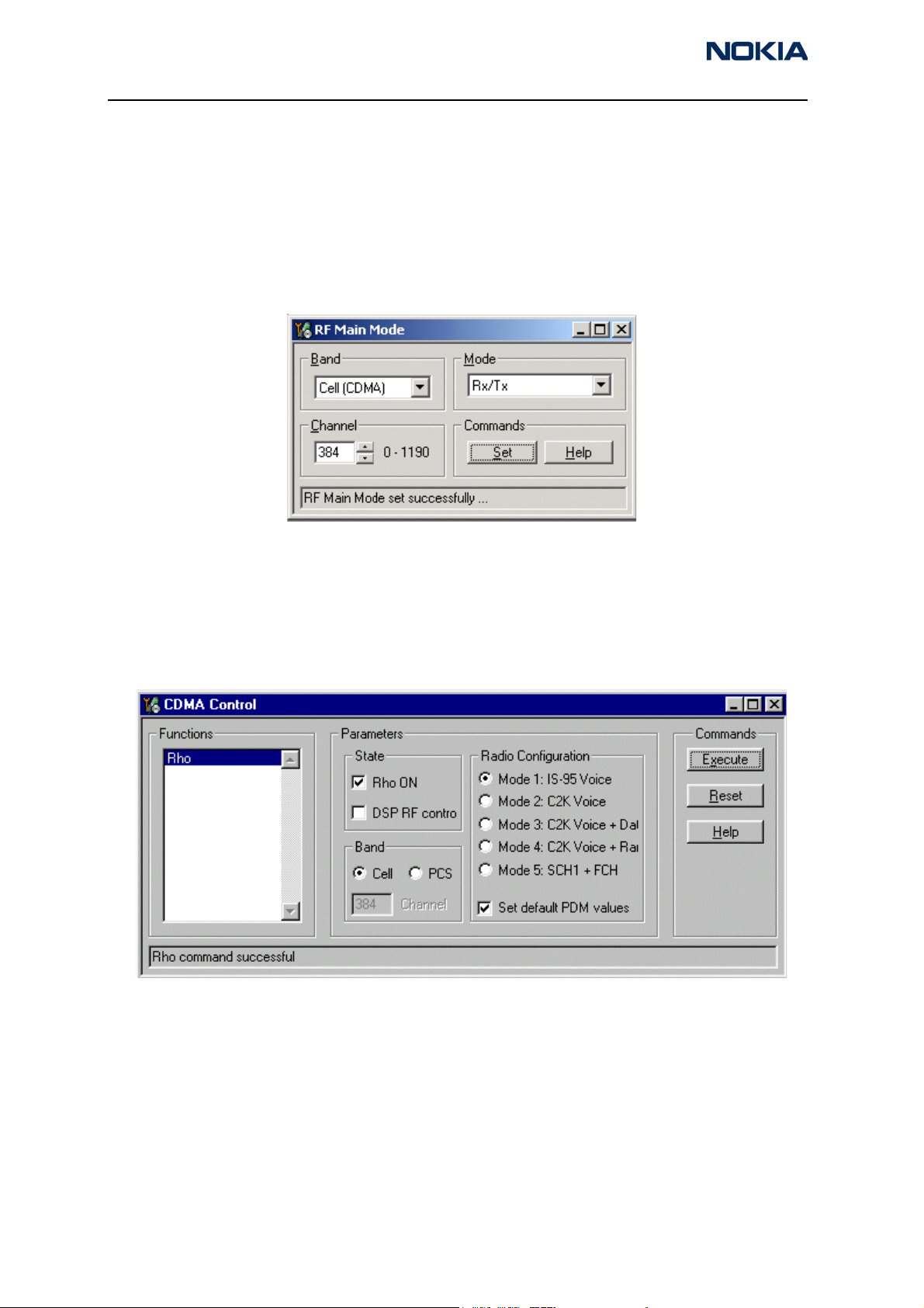
3. Select the following values on the RF Main Mode dialog box:
• Band = Cell (CDMA)
• Channel = 384
• Mode = Rx/Tx
Figure 4: RF Main Mode dialog box for Tx troubleshooting
4. Click Set.
Note: Be sure that the “RF Main Mode set successfully” message appears in the
status bar.
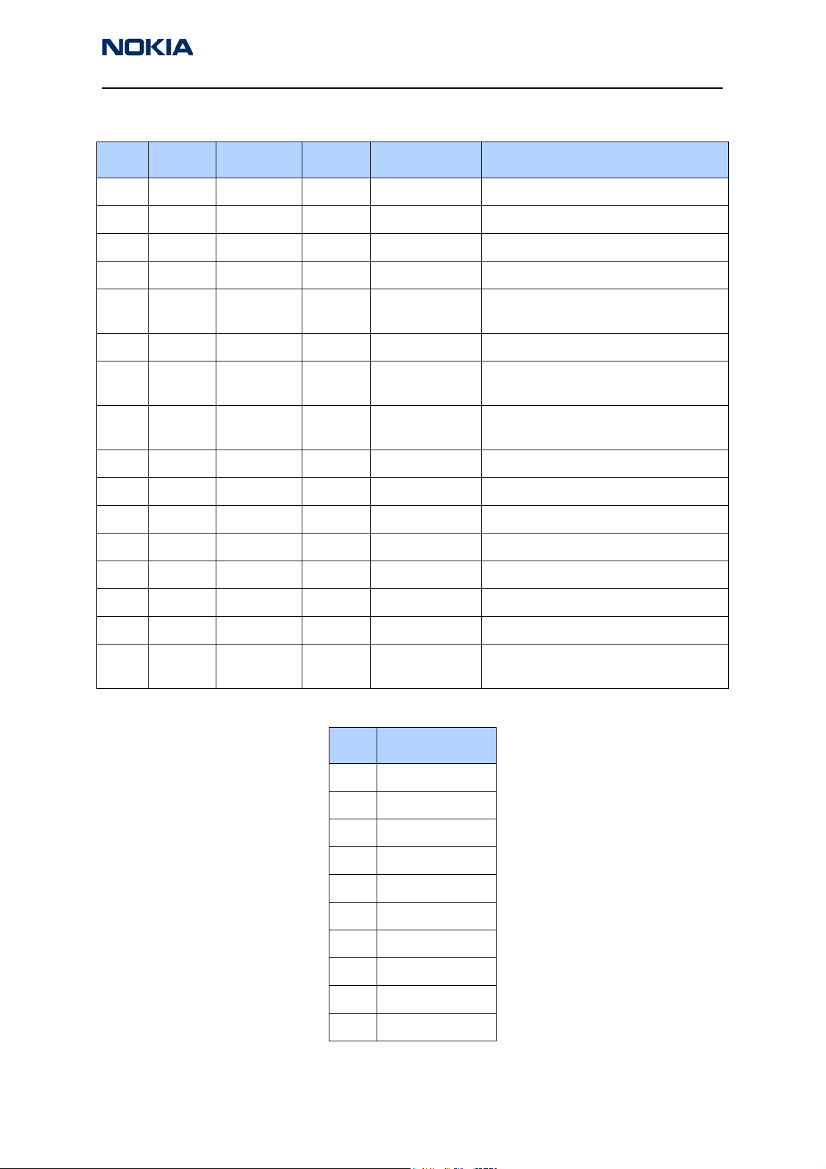
5. Select the Rho ON check box on the CDMA Control dialog box.
Figure 5: CDMA Control dialog box for Tx troubleshooting
6. Click Execute.
7. At this point you should be able to measure Tx Pout at the RF connector. The cell
band Tx Pout =0 to 2 dBm. If you do not see these values, set the AGC PDM for
25 dBm and probe the Tx path to figure out where in the path the fault occurs.
8. Open the General I/O dialog box to set the PA gain state.
Page 6 ©2005 Nokia Corporation Company Confidential Issue 01 04/2005
Page 7

2118 (RH-77)
Nokia Customer Care RF Description and Troubleshooting
9. Enter 10, 13, 12, and 8 in the PIN # fields.
Figure 6: General I/O dialog box for Tx troubleshooting
10. Select the boxes in the Enable column for each pin.
11. Click the Get All button.
12. Ensure that all of the pins have a value of H in the State column. (Click the L
values to change them to H values.)
13. Adjust the following PDM field values on the RF PDM dialog box:
• Tx IF AGC = -280
• Tx RF AGC = -280
Issue 01 04/2005 ©2005 Nokia Corporation Company Confidential Page 7
Page 8

2118 (RH-77)
RF Description and Troubleshooting Nokia Customer Care
Figure 7: RF PDM dialog box for Tx troubleshooting
14. Ensure that the Phone Tx Pout = +25 dBm and the current = 770-860 mA.
Cell Transmitter Path
Table 1 indicates the test points (see Figure 8) to probe when troubleshooting the cell
transmitter path. It is recommended that you follow the steps in order. An HP high
frequency probe was used to make the frequency and output power measurements
Table 1: Cell Transmitter Test Points
Typical
Test
Point
T1 Z601 pin1 N601-Out -43 dBm/
T2 Z601 pin 3 PA-In -25 dBm/
T3 N803 pin 8 PA-Out 5.0 dBm/
Part* Function
Value/
Frequency
HP85024A
836.52 MHz
836.52 MHz
836.52 MHz
Typical
Value
Frequency
Prod Probe
-13.2 dBm/
836.52 MHz
-15.4 dBm/
836.52 MHz
18.3 dBm/
836.52 MHz
Comments
Output of N601 Driver, Input to
Tx SAW Filter
Output of Tx SAW, Input to PA
Output of PA, Input to Isolator
T4 Z803T Iso-Out 2.2 dBm/
836.52 MHz
T5 C603L IF-Out -29 dBm/
228.6 MHz
T6 C638T, C654T,
C633R,
C635R,
C603LR
T7 C655R VR7 2.7 V dc UHF PLL Supply from UEM
VR5 2.7 V dc VHF VCO/PLL, IQ modulator
10.3 dBm/
836.52 MHz
-24 dBm/
228.6 MHz
Output of Isolator, Input to
Duplexer
Tx IF Probing Point at IF Filter
supply from UEM
Page 8 ©2005 Nokia Corporation Company Confidential Issue 01 04/2005
Page 9

2118 (RH-77)
Nokia Customer Care RF Description and Troubleshooting
Table 1: Cell Transmitter Test Points (Continued)
Typical
Test
Point
Part* Function
Value/
Frequency
HP85024A
T8 C636L, C624T,
L609B, C612L,
C630B, L607B
T9 C605R, C606R VAGC-Tx 0.2 to 1.8 V dc Tx AGC Control Voltage from
T10 C658R, C600T VIO-Tx 1.8 V dc Supply for Digital circuits from
T11 C805B, C810T,
C816R
T12 C802L, C813L VPA 3.6 V dc
T13 C814R VG 1.8 V dc
VR2 2.7 V dc Mixer, driver, and IF supply from
VBAT 3.6 V dc Battery Voltage
(High Gain)
(Enable)
Typical
Value
Frequency
Prod Probe
Comments
UEM
UPP.
0.2 V = Max Gain
1.8 V = Min Gain
UEM
(Nominal Voltage 3.6 V dc)
Main PA Supply Voltage from
PMIC. Lgain=0.8 V,
Mgain=-1.25 V, Hgain=Vbat
PA Gate Voltage (Enable/Disable)
Disable=0 V
* The R, L, T, and B values at the end of the part names indicate the Right, Left, Top,
and Bottom side of the part respectively in Figure 8 and Figure 9.
Issue 01 04/2005 ©2005 Nokia Corporation Company Confidential Page 9
Page 10

2118 (RH-77)
RF Description and Troubleshooting Nokia Customer Care
Figure 8 shows each test point for the N601 TXIC section from Table 1, “Cell Transmitter
Test Points,” on page 8. Always attach a 20 dB pad (11881-60001) when probing with an
HP85024A high-frequency probe.
Figure 8: (Top) PWB. (Bottom left) A zoomed view of the testing points on the N601 TXIC section.
(Bottom right) A zoomed view of the N601 TXIC section with part numbers.
Page 10 ©2005 Nokia Corporation Company Confidential Issue 01 04/2005
Page 11

2118 (RH-77)
Nokia Customer Care RF Description and Troubleshooting
Figure 9 shows each testing point for the PA section from Table 1, “Cell Transmitter Test
Points,” on page 8. Always attach a 20 dB pad (11881-60001) when probing with an
HP85024A high frequency probe.
Figure 9: (Top) PWB. (Bottom left) A zoomed view of the testing points on the PA section.
Tx AGC Tuning
Tx power versus IF/RF PDM can be verified against FlaLi specification limits. Make sure
that the PA is set in high gain mode (GenIO bits 10, 13, and 12 are set to H).
(Bottom right) A zoomed view of the PA section with part numbers.
Table 2: Tx AGC Tuning Steps
Tx Tuning
AGC Step
Tx AGC (0) 308 -46 -55 -37
Tx AGC (1) 130 -24 -34 -14
Tx AGC (2) 85 -15 -25 -6
Tx AGC (3) 51 -4.5 -14 5
Tx AGC (4) 19 2.5 -7 12
Tx AGC (5) -5 6 -3 15
Tx AGC
PDM Value
Target
Power
Low
Limit
High
Limit
Issue 01 04/2005 ©2005 Nokia Corporation Company Confidential Page 11
Page 12

2118 (RH-77)
RF Description and Troubleshooting Nokia Customer Care
Table 2: Tx AGC Tuning Steps (Continued)
*Not an actual FlaLi tuning PDM. The PDM produces approximately 25 dBm at the antenna
connector.
Cell Power Amplifier
The power amplifier (PA) has the DC/DC converter (PMIC device), which controls the
transmitter. The following tables show the circuits that have an effect on the transmitter
path and how to troubleshoot them.
Tx Tuning
AGC Step
Tx AGC (6) -94 15 6 24
Tx AGC (7)* -280* 25 21 27
Tx AGC
PDM Value
Table 3: PA Power and Gain Measurements
Power Amp
Input Test Point
pin3-Z601 left-R814
Table 4: PA Power and Gain Specifications
Target
Power
Low
Limit
Power Amp
Output Test Point
High
Limit
Mode Name
Gain mode 0 V0 up to 6 23.8 0.75- 0.88 C806
Gain mode 1 V1 6 to 11 25.2 1.125- 1.375 C806
Gain mode 3 V2 Not used Not used 2 - 2.5 C806
Gain mode 2 Bypass 11 up 29 3 - 4 C806
Gain mode 0 V0 up to 6 23.8 0.75- 0.88 C806
Gain mode 1 V1 6 to 11 25.2 1.125- 1.375 C806
Power Output
Range
Nominal Gain Vcc Range Vcc Test Point
*Not an actual FlaLi tuning PDM. PDM to produce approximately 25 dBm at
antenna connector.
Cell PMIC
The following tables show the PMIC troubleshooting information.
Table 5: PMIC Setup
Mode Tx Rx Band
Local On On CELL
Page 12 ©2005 Nokia Corporation Company Confidential Issue 01 04/2005
Page 13
2118 (RH-77)
Nokia Customer Care RF Description and Troubleshooting
Table 6: PMIC Measurements
Pin Label Test Point Units Depends On Comments
1 EP Pin 1 1.8 UPP IC enable = GenIO 10
2 M0 Pin 2 1.8 UPP Control 0 = GenIO 12
3 M1 Pin 3 1.8 UPP Control 1 = GenIO 13
4NC NC NC NC NC
5 FB Pin 5 0.75 - 4 M0, M1 See PA worksheet. Output to flyback
inductor.
6 FB Pin 6 0.75 - 4 M0, M1 Shares PWB pad with pin 5
7 BYPVout bottom-
C808
8 VDD right-L810 VBATT VBATT Digital DC supply, shared with pin 12,
9 VSS GND GND GND Digital GND, shared gnd with pin 13
10 NC NC NC NC NC
11 Vbgap NC NC NC Bandgap voltage output
12 VDD right-L810 VBATT VBATT Digital DC supply
13 Vss GND GND GND Digital GND, shared gnd with pin 9
14 Vsw right-L810 VBATT VBATT Switcher supply
15 Vsw right-L810 VBATT VBATT Switcher supply
16 Gsw GND GND GND Switcher GND, does not share with pin 9
0.75 - 4 M0, M1 PMIC bypass output used at
Pout > 12 dBm
14, and 15
and pin 13
Table 7: Good Mobile Terminal PMIC Resistances
Pin Resistance
1 60 k
2 75 k
3 80 k
4 1.59 M
51.6 M
62 M
72 M
82 M
90.1
10 100
Issue 01 04/2005 ©2005 Nokia Corporation Company Confidential Page 13
Page 14

2118 (RH-77)
RF Description and Troubleshooting Nokia Customer Care
Table 7: Good Mobile Terminal PMIC Resistances (Continued)
Pin Resistance
11 115 k
12 60 k
13 0.2
14 1.3 M
15 1.18 M
16 0.1
Cell IF/RF AGC and PA Control
Table 8, “Cell CDMA Channel 384 (Skyworks PA),” on page 15 illustrates the PDM values
and their typical values for the IF AGC, RF AGC N601 Pout, gain steps, and the PA VCC
levels. This table also shows the typical power output at the RF connector.
Page 14 ©2005 Nokia Corporation Company Confidential Issue 01 04/2005
Page 15

2118 (RH-77)
Nokia Customer Care RF Description and Troubleshooting
Table 8: Cell CDMA Channel 384 (Skyworks PA)
Tx RF AGC Tx IF AGC N601 Po PA Gain Step PA Vcc
Conn RF
PDM
Typical
Value
Test
Point
PDM
Typical
Value
Test
Point
Typical
Value
Test
Point
Gen IO 12 Gen IO 13
Typical
Value
Test
Point
PA
Gain
Pout
-290 0.45 Bottom
C606
-196 0.59 -196 0.59 -2 H H 3.61 28 20
-95 0.75 -95 0.75 -9.2 H H 3.67 28 13.2
-95 0.75 -95 0.75 -9.2 H L 1.2 26 11
-48 0.83 -48 0.83 -13 H L 1.2 25.8 7
-48 0.83 -48 0.83 -13 L L 0.82 24.5 6
17 0.93 17 0.93 -19 L L 0.82 0
80 1.04 80 1.04 -29 L L 0.82 -10
120 1.11 120 1.11 -39 L L 0.82 -20
168 1.19 168 1.19 -49 L L 0.82 -30
249 1.32 249 1.32 -59 L L 0.82 -40
324 1.49 324 1.49 -69 L L 0.82 -50
-290 0.45 Top
C605
3pin 1
Z601
H H 3.47 C806 DM 25
Issue 01 04/2005 ©2005 Nokia Corporation Company Confidential Page 15
Page 16

2118 (RH-77)
RF Description and Troubleshooting Nokia Customer Care
Cell Power Detector
The following tables illustrate the measurements required for troubleshooting the cell
power detector.
Table 9: Cell Power Setup
Mode Tx Rx Band Chnn Rho
Local On On CELL 384 On
Input Chnn Tx Freq Rx Freq
384 836.52 881.52
Table 10: Cell Power Measurements: Cell, Channel 384
Tx ADC
RF/IF
pdm
324 L L -50 -86.3 Right
142 L L -25 -63 2 235
17 L L 0 -41 1.998 235
-48 L L 6 -30 1.967 250
-48 H L 7 -29 1.957 268
-95 H L 11 -26 1.93 286
-95 H H 13.2 -23.5 1.9 435
-146 H H 17 -21.5 1.86 486
-178 H H 19 -19 1.812 550
PA Gain
Step
GIO 12GIO
13
Conn
RF Pout
Pout at
Detector
Power Detector Comments
Test
Point
R814
Det
Out
2Left
Test
Point
C807
mA
235 Cell band and
Det=Detector
Po=Power
detector
coupling is about
22 dB
-214 H H 21 -17 1.745 630
-252 H H 23 -15 1.667 730
-290 H H 25 -12 1.547 860
-316 H H 26 -11.5 1.485 950
-328 H H 26.5 -11 1.44 1000
-351 H H 27.5 -10 1.36 1095
none dBm dBm/
30kHz
VDC dBm only refers
to total power
measured
Page 16 ©2005 Nokia Corporation Company Confidential Issue 01 04/2005
Page 17

2118 (RH-77)
Nokia Customer Care RF Description and Troubleshooting
Table 11: Detector Reference and DC Supply
label Test Point Typical Value
Det Ref left-C803 2
Det Supply bottom-C257 2.8
VDC
Issue 01 04/2005 ©2005 Nokia Corporation Company Confidential Page 17
Page 18

2118 (RH-77)
RF Description and Troubleshooting Nokia Customer Care
Tx System Block Diagram
See the Schematics chapter for a 2118 transmitter schematic.
Antenna
Antenna
Antenna
Antenna
I
I
I
From
From
From
From
Baseband
Baseband
Baseband
Baseband
Q
Q
Q
BB I LPF
457.2MHz
VHF LO
VHF LO
VHF LO
VHF LO
÷2/÷4
÷2/÷4
÷2/÷4
÷2/÷4
IQ Modulator
0º
0º
0º
90º
90º
90º
90º
IF VGA
(IF AGC PDM)
UHF LO
UHF LO
UHF LO
0º
0º
0º
0º0º
90º
90º
90º
1052.61-107757MHz
Upconverter
0º
0º
0º
0º
0º
0º
0º0º
90º
90º
90º
90º
90º
90º
90º
90º
RF VGA
(RF AGC PDM)
TP1
Bandpass
Tx SAW
To Baseband
To Baseband
To Baseband
PWR Amplifier
TP2 TP3
Power
Power
Power
Power
Detector
Detector
Detector
Detector
Isolator
Isolator
Isolator
TP4
Cell RX
Cell RX
Cell RX
Cell RX
Duplexer
Duplexer
Duplexer
Duplexer
Figure 10: Tx system block diagram
Page 18 ©2005 Nokia Corporation Company Confidential Issue 01 04/2005
Page 19

2118 (RH-77)
Nokia Customer Care RF Description and Troubleshooting
Receiver Troubleshooting
Rx IF
Use Phoenix to perform the following steps for troubleshooting the receiver. Together
with the VCO frequency and level verification, this test should be the first test for a nonworking receiver. This test verifies the entire receiver chain, from input connector to
baseband output.
1. Inject a CW signal 881.82 MHz or 881.22 MHz (CH-384 offset by 300 KHz) at a
fixed –75 dBm power level. If you do not have a signal generator, use the call box
in AMPS mode on Channel 374 or 394 (10 channels away from channel 384).
2. Open the Phone Control dialog box.
Figure 11: Phone Control dialog box for Rx IF troubleshooting
3. Click the LOCAL button in the Phone State area to put the mobile terminal into
Local Mode.
4. Select the following values on the RF Main Mode dialog box:
• Band = Cell (CDMA)
• Channel = 384
• Mode = Rx
Issue 01 04/2005 ©2005 Nokia Corporation Company Confidential Page 19
Page 20

2118 (RH-77)
RF Description and Troubleshooting Nokia Customer Care
Figure 12: RF Main Mode dialog box for Rx IF troubleshooting
5. Click Set.
Note: Be sure that the “RF Main Mode set successfully” message appears in
the status bar.
6. Use a spectrum analyzer to test TP3 (I+,I-, Q+, Q-). Set the S.A to 300 KHz center
frequency, 200 KHz SPAN, and +10 dBm reference level. The spectrum analyzer
should read –8 dBm without any settings to the PDM.
7. Use Table 12 to configure the CDMA generator code domain.
Table 12: CDMA Generator Code Domain Setup
Channel Power Walsh Code
Pilot -7dB 0
Paging -12dB 1
Traffic -15.6dB 10
Sync -16dB 32
Table 13 shows the steps for Rx IF troubleshooting. See Figure 13 on page 22 for an
illustration of the corresponding test points.
Step # Part Function
Table 13: Rx IF Troubleshooting
Typical
Value/
Frequency
HP85024A
Typical
Value
Frequency
Prod Probe
Comments
TP1 L702R IF-IN +1.3 dBm/
183.6MHz
TP2 L701L/R SAW Out -16 dBm/
183.6MHz
-12/-27 dBm
183.6 MHz
-35/-50 dBm
183.6 MHz
I.F Input to Z701 (I.F filter).
NOT 50 ohm
Differential outputs of Z701.
NOT 50 ohm
Page 20 ©2005 Nokia Corporation Company Confidential Issue 01 04/2005
Page 21

2118 (RH-77)
Nokia Customer Care RF Description and Troubleshooting
Table 13: Rx IF Troubleshooting (Continued)
Typical
Step # Part Function
Value/
Frequency
HP85024A
TP3 I+, I-, Q+, Q- I/Q outputs
of N700
TP4 C728T 19.2MHz In +6.5 dBm
TP5 C711T 19.2MHz Out +4 dBm
TP6 L708R (L708R
for Prod
Probe)
TP7 C731T VREF 1.35 Vdc System reference voltage
VHF VCO +1.0 dBm
300KHz tone
for input:
881.22 MHz
19.2 MHz
19.2 MHz
367.2 MHz
Typical
Value
Frequency
Prod Probe
-69/-84 dBm
300 KHz
-22 dBm
19.2 MHz
-25 dBm
19.2 MHz
-61 dBm
367.2 MHz
Comments
Baseband differential
outputs of the IF IC (N700).
To test: set the input to
881.22 or 881.82 MHz/-75
dBm to get a 300 KHz tone
when receiver is on channel
384 (881.52 MHz)
Sine wave input to N700
from VCTCXO.
Square wave output of N700
to baseband.
Rx VHF VCO - Fixed at 367.2
MHz (Be careful not to load
the circuit with the probe.)
1.35 Vdc from UEM.
TP8 R702L
(C703R)
TP9 R703T (R701L,
R715T)
TP10 C734B VR3 2.7 Vdc VCTCXO buffer supply from
TP11 C712R, C744R VR6 2.7 Vdc Main supply to N700, from
TP12 C710T, C704B VIO 1.8 Vdc Digital circuits supply from
RX_IF_AGC 0.2 to 1.8 Vdc AGC control Voltage. 0.2V =
Max Gain, 1.8 V = Minimum
Gain
VR7 2.7 Vdc VHF VCO Supply from UEM
UEM.
UEM.
UEM.
* The R, L, T, and B values at the end of the part numbers indicate the Right, Left,
Top, and Bottom side of the part respectively in Figure 13.
Issue 01 04/2005 ©2005 Nokia Corporation Company Confidential Page 21
Page 22

2118 (RH-77)
RF Description and Troubleshooting Nokia Customer Care
Figure 13 shows each test point as listed in Table 13.
Figure 13: (Top) PWB. (Bottom left) A zoomed view of the testing points on the Rx IF section.
(Bottom right) A zoomed view of the Rx IF section with part numbers.
Page 22 ©2005 Nokia Corporation Company Confidential Issue 01 04/2005
Page 23

2118 (RH-77)
Nokia Customer Care RF Description and Troubleshooting
Figure 14 shows an alternate part orientation. Notice that Pin 1 is rotated 180 degrees
compared to the first filter as shown in Figure 13 on page 22. All test points and values
are the same.
Figure 14: Alternate part orientation with pin 1 rotated 180 degrees
Issue 01 04/2005 ©2005 Nokia Corporation Company Confidential Page 23
Page 24

2118 (RH-77)
RF Description and Troubleshooting Nokia Customer Care
Switching the Gain
Use the following steps if the receiver is not working properly and you need to switch the
Rx gain state.
1. Open the Phone Control dialog box.
Figure 15: Phone Control dialog box for switching the Rx gain state
2. Click the LOCAL button in the Phone State area to put the mobile terminal into
Local Mode.
3. Select the following values on the RF Main Mode dialog box:
• Band = Cell (CDMA)
• Channel = 384
• Mode = Rx
Figure 16: RF Main Mode dialog box for switching the Rx gain state
4. Click Set.
Note: Be sure that the “RF Main Mode set successfully” message appears in
the status bar.
Page 24 ©2005 Nokia Corporation Company Confidential Issue 01 04/2005
Page 25

2118 (RH-77)
Nokia Customer Care RF Description and Troubleshooting
5. Connect a signal generator in CW mode (881.52 MHz, -25 dBm) to the RF
connector. If you do not have a generator, use the Call Box Amps Mode RF
Generator, Channel 384, -25 dBm and set the FM modulation to 100 Hz,
deviation 400 Hz.
6. To switch the Rx gain states, open the RF Register R/W dialog box. Two gain
states (Hi and Lo) are available in the receiver.
High gain state
Figure 17: RF Register R/W dialog box for switching Rx gain states
7. Select the appropriate gain states from Register #6. The following values apply:
• Bit 0=1, means a Hi gain state.
• Bit 0=0, means a Lo gain state.
Issue 01 04/2005 ©2005 Nokia Corporation Company Confidential Page 25
Page 26

2118 (RH-77)
RF Description and Troubleshooting Nokia Customer Care
Rx RF
The following Rx RF Troubleshooting table indicates the test points to probe when
troubleshooting the Rx RF. It is recommended that you follow the steps in order. See
Figure 18 on page 27 for an illustration of the test points.
Table 14: Rx RF Troubleshooting
Typical
Step # Part Function
Value/
Frequency
HP85024A
R1 L802R (Top
side of the
PWB)
R2 L906L LNA-In -35dBm/
R3 C903L LNA-Out -13/-31dBm
R4 Z901-R-
Bottom,
N901-Pin16
R5 C906R Mixer-out -5/-21dBm
R6 C912B/R914R IF Output to
R7 R912B/R911L L.O Input to
RF-IN -25 dBm/
881.52 MHz
881.52MHz
881.52MHz
RF Filter Output
Mixer-In
N700
N901
-18/-35dBm
881.52MHz
183.6 MHz
+1.5/-15dBm
183.6MHz
-2.5dBm
1065.12MHz
Typical
Value
Frequency
Prod Probe
-42 dBm
881.52 MHz
-42dBm
881.52MHz
-29/-45dBm
881.52MHz
-30/-45dBm
881.52MHz
-23/-38dBm
183.6MHz
-12/-29dBm
183.6MHz
-18dBm
1065.12MHz
Comments
Input Connector reference
level
Test Duplexer insertion Loss
(Without DC Block)
Test LNA gain ~ 13dB
Test RF Filter Insertion loss
(Without DC Block)
Test Output on
Downconverter on N901
Test N2302 output to N700
IF-IC
Test VCO output to N2302
Levels are for Channel 384
R8 R9056T,
L909L, L901T,
R910B
R9 R902B Rx-SW1 H.G = 2.7V
VR4 2.7V dc Power supply to N2302
L.G = 0V
* The R, L, T, and B values at the end of the part names indicate the Right, Left, Top,
and Bottom side of the part respectively in Figure 18.
LNA gain control, on the
N2302 side, High Gain >
2.5V dc
Page 26 ©2005 Nokia Corporation Company Confidential Issue 01 04/2005
Page 27

2118 (RH-77)
Nokia Customer Care RF Description and Troubleshooting
Antennae
Connector
(top side)
R1
Figure 18: (Top left) PWB. (Top right) The antenna connector on the opposite side of the PWB, (Bottom left)
A zoomed view of the testing points on the Rx RF section. (Bottom right) A zoomed view of the Rx RF section
with part numbers.
Issue 01 04/2005 ©2005 Nokia Corporation Company Confidential Page 27
Page 28

2118 (RH-77)
RF Description and Troubleshooting Nokia Customer Care
Rx AGC (Cell mode)
The following Rx RF AGC PDM vs. AGC Voltage table shows the Rx RF AGC PDM vs. AGC
voltages in local mode on channel 384.
Table 15: Rx RF AGC PDM vs. AGC Voltage
PDM Typical Value Test Point
-512 0.08 right R702
-400 0.260
-300 0.436
-200 0.597
-100 0.753
00.913
100 1.076
200 1.24
300 1.403
350 1.494
400 1.570
500 1.740
511 1.761
UNITS VDC
Table 16: Rx AGC vs. RF Pin for CELL Band
Conn RF Pin CELL RF AGC Comments
-25 1.492
-35 1.298
-45 1.159 In Normal mode, the mobile terminal will adjust RF RX AGC
-55 1.019 Rx power is coming in, the I and Q will be about 0.5Vpp and 1.3V
-65 0.861
-75 0.705 Approximately 1pdm per 1mV
-85 0.530
-92 0.425
-95 0.633 Note the reduced delta because the LNA is switched on
-100 0.594
-105 0.524
Page 28 ©2005 Nokia Corporation Company Confidential Issue 01 04/2005
Page 29

2118 (RH-77)
Nokia Customer Care RF Description and Troubleshooting
Table 16: Rx AGC vs. RF Pin for CELL Band (Continued)
Conn RF Pin CELL RF AGC Comments
-107 0.470
UNITS VDC
Issue 01 04/2005 ©2005 Nokia Corporation Company Confidential Page 29
Page 30

2118 (RH-77)
÷
RF Description and Troubleshooting Nokia Customer Care
Receiver Block Diagram
See the Schematics chapter for a 2118 receiver schematic.
LNA SW Control
I/Q Down
Converter
CDMA
BB Filter
TX
Antenna
Duplexer
LNA
CELL
SAW
Loop Filter
RFA
UHF VCO
1052.61-1077.57
UHF Synthsizer
JEDI
IFA
IF SAW
VCTCXO
VGA
CDMA
BB Filters
2
BB AMP
To BB
BB AMP
VHF PLL
367.2 MHz
Bias and Control
Reference Clock
To Base-Band
AFC
Figure 19: Receiver block diagram
Page 30 ©2005 Nokia Corporation Company Confidential Issue 01 04/2005
Page 31

2118 (RH-77)
Nokia Customer Care RF Description and Troubleshooting
Synthesizer Troubleshooting
Faulty synthesizers can cause both Rx and Tx failures during tuning, in addition to the
VCTCXO tuning. The following synthesizers are incorporated into the mobile terminal:
• UHF (cell) PLL inside N601 IC
• Tx VHF (457.2MHz) with PLL in N601 IC in Cell Mode
• Tx VHF (527.2MHz) with PLL in N601 IC in PCS Mode
• Rx VHF (367.2MHz) with PLL in N700 IC
Synthesizer Setup
Use the following steps to set up the mobile terminal for Tx troubleshooting in Phoenix.
1. Open the Phone Control dialog box.
Figure 20: Phone Control dialog box for Tx troubleshooting
2. Click the LOCAL button in the Phone State area to put the mobile terminal into
Local Mode.
3. Use the following settings for the Band, Channel, and Mode fields on the RF
Main Mode dialog box:
• UHF: Use the Rx/Tx mode and channel 384 in Cell band. This allows you to
check power in both the Rx and Tx circuits.
• Rx VHF: Use the Rx mode. One band is enough.
• Tx VHF: Use the Rx/Tx mode in Cell band.
Issue 01 04/2005 ©2005 Nokia Corporation Company Confidential Page 31
Page 32

2118 (RH-77)
RF Description and Troubleshooting Nokia Customer Care
Figure 21: RF Main Mode dialog box for synthesizer troubleshooting
4. Click Set.
Note: Be sure that the “RF Main Mode set successfully” message appears in
the status bar.
5. Read register templates N601(0) bits 10 and 11 for the UHF and Tx VHF lock
condition on the RF Register R/W dialog box.
Figure 22: RF Register R/W dialog box for synthesizer setup
6. Read register templates N700(0) bit 11 for the RX VHF lock condition.
Page 32 ©2005 Nokia Corporation Company Confidential Issue 01 04/2005
Page 33

2118 (RH-77)
Nokia Customer Care RF Description and Troubleshooting
VCTCXO Tuning
The VCTCXO can be manually tuned to verify failed tuned mobile terminals, or to verify if
a mobile terminal cannot make a call. This can be done with the mobile terminal in Local
Mode and generating a CW signal. The frequency accuracy of the VCTCXO can be
measured using an HP8960 callbox in AMPS mode, an HP4406 Tx tester, or a spectrum
analyzer (preferably using a lab system 10MHz source as equipment reference). Replace
the VCTCXO if the VCTCXO AFC DAC value does not meet the tuning requirements after
tuning.
Use the following steps to manually tune the VCTCXO:
1. Open the Phone Control dialog box.
Figure 23: Phone Control dialog box for VCTCXO troubleshooting
2. Click the LOCAL button in the Phone State area to put the mobile terminal into
Local Mode.
3. Select the following values on the RF Main Mode dialog box:
• Band = Cell (CDMA)
• Channel = 384
• Mode = Rx/Tx
Issue 01 04/2005 ©2005 Nokia Corporation Company Confidential Page 33
Page 34

2118 (RH-77)
RF Description and Troubleshooting Nokia Customer Care
Figure 24: RF Main Mode dialog box for VCTCXO troubleshooting
4. Do not use CDMA control to turn on Rho.
5. Open the BB General I/O dialog box to set the CW signal.
6. Type 10, 13, 12, and 8 in the fields in the PIN # column.
Figure 25: General I/O dialog box for VCTCXO tuning
7. Click the Get All button.
8. Change the value for Pin 8 in the Source column to GenIO Output.
9. Ensure that all of the pins have a value of H in the State column. (Click the L
values to change them to H values.)
Page 34 ©2005 Nokia Corporation Company Confidential Issue 01 04/2005
Page 35

2118 (RH-77)
Nokia Customer Care RF Description and Troubleshooting
10. The next step depends on the type of measurement equipment you are using:
• HP4406 or a spectrum analyzer: Set the center frequency to 836.52MHz and
the span to 2MHz. Also, establish a marker at 836.52MHz.
• HP8960: Set the callbox state to AMPS, and set the channel to 384. Use the
Frequency Accuracy measurement to center the VCTCXO.
11. Adjust the AFC value to center the VCTCXO on the RF PDM dialog box. The
tuning range is approximately +/- 10kHz.
Figure 26: Manually adjusting the AFC to center VCTCXO
12. Adjust the AFC value so that the output signal is within +/- 100Hz. If you are
using an HP4406 or a spectrum analyzer, narrow the span to 1kHz or less.
Issue 01 04/2005 ©2005 Nokia Corporation Company Confidential Page 35
Page 36

2118 (RH-77)
RF Description and Troubleshooting Nokia Customer Care
VCTCXO Reference Clock
Figure 27 shows the 19.2 MHz VCTCXO reference clock.
To
Figure 27: (Top) PWB. (Bottom left) A zoomed view of the testing points on the 19.2 MHz VCTCXO reference
clock. (Bottom right) A zoomed view of the 19.2 MHz VCTCXO reference clock with part numbers.
To PLL
Page 36 ©2005 Nokia Corporation Company Confidential Issue 01 04/2005
Page 37

2118 (RH-77)
Nokia Customer Care RF Description and Troubleshooting
Synthesizer Block Diagram
See the Schematics chapter for the synthesizer schematic.
CELL:457.2MHz
CELL:457.2MHz
JEDI
JEDI
367.2MHz
367.2MHz
VHF
VHF
counter
counter
Yoda
Yoda
19.2MHz
19.2MHz
VCTCXO
VCTCXO
19.2MHz to
19.2MHz to
UPP
UPP
VHF
VHF
counter
counter
UHF
UHF
counter
counter
CELLlBand UHF VCO
CELLlBand UHF VCO
Figure 28: Synthesizer block diagram
Issue 01 04/2005 ©2005 Nokia Corporation Company Confidential Page 37
Page 38

2118 (RH-77)
RF Description and Troubleshooting Nokia Customer Care
UHF Synthesizer
Following are possible causes for an incorrect UHF frequency:
• Orientation of N601
• Power supplies to N601 PLL are missing or low (VR7)
• Loop filter components are missing or incorrectly installed
• Matching components to N601 TxLO/PLL input are missing or incorrectly
installed
• 19.2MHz reference clock is missing or low
• Programming is incorrect
• Component failure (VCO or PLL portion of N601)
Figure 29 and Figure 30 show the UHF synthesizer layout.
Figure 29: (Top) PWB. (Bottom left) A zoomed view of the testing points on the UHF synthesizer layout.
(Bottom right) A zoomed view of the UHF synthesizer layout with part numbers.
Page 38 ©2005 Nokia Corporation Company Confidential Issue 01 04/2005
Page 39

2118 (RH-77)
Nokia Customer Care RF Description and Troubleshooting
LO PLL
Figure 30: (Top) PWB. (Bottom left) A zoomed view of the N601 LO/PLL input match components on the UHF
synthesizer layout (Bottom right) A zoomed view of the N601 LO/PLL input match components UHF
synthesizer layout with part numbers.
Rx VHF
Following are possible causes for an incorrect Rx VHF frequency:
• Power supplies to the PLL portion of N700 IC are missing or low (VR7)
• Loop filter or resonator components are missing or incorrectly installed
• 19.2MHz reference clock is missing or low (C510)
• Programming is incorrect
Note: See the Schematics chapter for the Rx VHF schematic.
Issue 01 04/2005 ©2005 Nokia Corporation Company Confidential Page 39
Page 40

2118 (RH-77)
RF Description and Troubleshooting Nokia Customer Care
Figure 31 shows the layout for the Rx VHF.
Figure 31: (Top) PWB. (Bottom left) A zoomed view of the testing points on the Rx VHF section.
(Bottom right) A zoomed view of the Rx VHF section with part numbers.
Tx VHF
Following are possible causes for an incorrect Tx VHF frequency:
• Power supplies to the PLL portion of N601IC missing or low (VR5)
• Loop filter or resonator components are missing or incorrectly installed
• 19.2MHz reference clock is missing or low (C510)
• Programming is incorrect
• Component failure (N601 IC)
Note: See the Schematics chapter for the Tx VHF schematic.
IC with
Page 40 ©2005 Nokia Corporation Company Confidential Issue 01 04/2005
Page 41

2118 (RH-77)
Nokia Customer Care RF Description and Troubleshooting
Figure 32 shows the layout for the Tx VHF.
IC with
Figure 32: (Top) PWB. (Bottom left) A zoomed view of the testing points on the Tx VHF section.
(Bottom right) A zoomed view of the Tx VHF section with part numbers.
Issue 01 04/2005 ©2005 Nokia Corporation Company Confidential Page 41
Page 42

2118 (RH-77)
RF Description and Troubleshooting Nokia Customer Care
This page intentionally left blank.
Page 42 ©2005 Nokia Corporation Company Confidential Issue 01 04/2005
 Loading...