

Page 1

Nokia Customer Care
SERVICE
MANUAL
[NMP Part No. 9239059]
RH-66 Mobile Terminal
2115i/2116/2116i
Issue 1
COMPANY CONFIDENTIAL
Issue 1 03/2005
Copyright © 2005 Nokia. All Rights Reserved.
Page 2

Nokia Customer Care
Amendment Record Sheet
Revision Date Author Comments
001 03/2005 N. Cheshier Issue 1
Issue 1 03/2005 COMPANY CONFIDENTIAL 2
Copyright © 2005 Nokia. All Rights Reserved.
Page 3

Nokia Customer Care
Copyright© 2005 Nokia. All rights reserved.
Reproduction, transfer, distribution or storage of part or all of the contents in
this document in any form without the prior written permission of Nokia is
prohibited.
Nokia, Nokia Connecting People, X and Y are trademarks or registered
trademarks of Nokia Corporation. Other product and company names
mentioned herein may be trademarks or tradenames of their respective
owners.
Nokia operates a policy of continuous development. Nokia reserves the right to
make changes and improvements to any of the products described in this
document without prior notice.
Under no circumstances shall Nokia be responsible for any loss of data or
income or any special, incidental, consequential or indirect damages
howsoever caused.
The contents of this document are provided "as is". Except as required by
applicable law, no warranties of any kind, either express or implied, including,
but not limited to, the implied warranties of merchantability and fitness for a
particular purpose, are made in relation to the accuracy, reliability or contents
of this document. Nokia reserves the right to revise this document or withdraw
it at any time without prior notice.
The availability of particular products may vary by region.
IMPORTANT
This document is intended for use by qualified service personnel
only.
Issue 1 03/2005 COMPANY CONFIDENTIAL 3
Copyright © 2005 Nokia. All Rights Reserved.
Page 4

Please refer to the product’s user guide for instructions relating
to operation, care and maintenance including important safety
information. Note also the following:
Warnings:
1. IF THE DEVICE CAN BE INSTALLED IN A VEHICLE, CARE
MUST BE TAKEN ON INSTALLATION IN VEHICLES FITTED
WITH ELECTRONIC ENGINE MANAGEMENT SYSTEMS AND
ANTI-SKID BRAKING SYSTEMS. UNDER CERTAIN FAULT
CONDITIONS, EMITTED RF ENERGY CAN AFFECT THEIR
OPERATION. IF NECESSARY, CONSULT THE VEHICLE
DEALER/MANUFACTURER TO DETERMINE THE IMMUNITY
OF VEHICLE ELECTRONIC SYSTEMS TO RF ENERGY.
Nokia Customer Care
Warnings and Cautions
2. THE PRODUCT MUST NOT BE OPERA TED IN AREAS LIKEL Y
TO CONT AIN POTENTIALL Y EXPLOSIVE A TMOSPHERES EG
PETROL STATIONS (SERVICE STATIONS), BLASTING
AREAS ETC.
3. OPERATION OF ANY RADIO TRANSMITTING EQUIPMENT,
INCLUDING CELLULAR TELEPHONES, MAY INTERFERE
WITH THE FUNCTIONALITY OF INADEQUATELY PROTECTED MEDICAL DEVICES. CONSULT A PHYSICIAN OR
THE MANUFACTURER OF THE MEDICAL DEVICE IF YOU
HA VE ANY QUESTIONS. OTHER ELECTRONIC EQUIPMENT
MAY ALSO BE SUBJECT TO INTERFERENCE.
Cautions:
1. Servicing and alignment must be undertaken by qualified personnel only.
2. Ensure all work is carried out at an anti-static workstation and
that an anti-static wrist strap is worn.
3. Ensure solder, wire, or foreign matter does not enter the mobile
terminal as damage may result.
4. Use only approved components as specified in the parts list.
5. Ensure all components, modules screws and insulators are correctly re-fitted after servicing and alignment. Ensure all cables
and wires are repositioned correctly.
Issue 1 03/2005 COMPANY CONFIDENTIAL 4
Copyright © 2005 Nokia. All Rights Reserved.
Page 5

Nokia Customer Care
For Your Safety
QUALIFIED SERVICE
Only qualified personnel may install or repair mobile terminal equipment.
ACCESSORIES AND BATTERIES
Use only approved accessories and batteries. Do not connect incompatible
products.
CONNECTING TO OTHER DEVICES
When connecting to any other device, read its user’s guide for detailed safety
instructions. Do not connect incompatible products.
ESD Protection
Nokia requires that product service points have sufficient
ESD protection (against static electricity) when servicing
products.
Any product of which the covers are removed must be handled with ESD protection. The SIM card can be replaced
without ESD protection if the product is otherwise ready for
use.
To replace the covers ESD protection must be applied.
All electronic parts of the product are susceptible to ESD.
Resistors, too, can be damaged by static electricity discharge.
All ESD sensitive parts must be packed in metallized protective bags during shipping and handling outside any ESD
Protected Area (EPA).
Every repair action involving opening the product or handling the product components must be done under ESD
protection.
ESD protected spare part packages MUST NOT be
opened/closed out of an ESD Protected Area.
For more information and local requirements about ESD
protection and ESD Protected Area, contact your local
Nokia After Market Services representative.
Issue 1 03/2005 COMPANY CONFIDENTIAL 5
Copyright © 2005 Nokia. All Rights Reserved.
Page 6

Nokia Customer Care
Battery Information
Note that a new battery's full performance is achieved only after two or three
complete charge and discharge cycles.
The battery can be charged and discharged hundreds of times but it will
eventually wear out. When the operating time (talk-time and standby time) is
noticeably shorter than normal, it is time to buy a new battery.
Use only batteries approved by the mobile terminal manufacturer and recharge
the battery only with the chargers approved by the manufacturer. Unplug the
charger when not in use. Do not leave the battery connected to a charger for
longer than a week, since overcharging may shorten its lifetime. If left unused
a fully charged battery will discharge itself over time.
Temperature extremes can affect the ability of your battery to charge.
For good operation times with Ni-Cd/NiMh batteries, discharge the battery
from time to time by leaving the product switched on until it turns itself off (or
by using the battery discharge facility of any approved accessory available for
the product). Do not attempt to discharge the battery by any other means.
Use the battery only for its intended purpose.
Never use any charger or battery which is damaged.
Do not short-circuit the battery. Accidental short-circuiting can occur when a
metallic object (coin, clip or pen) causes direct connection of the + and terminals of the battery (metal strips on the battery) for example when you
carry a spare battery in your pocket or purse. Short- circuiting the terminals
may damage the battery or the connecting object.
Leaving the battery in hot or cold places, such as in a closed car in summer or
winter conditions, will reduce the capacity and lifetime of the battery. Always
try to keep the battery between 15°C and 25°C (59°F and 77°F). A mobile
terminal with a hot or cold battery may temporarily not work, even when the
battery is fully charged. Batteries' performance is particularly limited in
temperatures well below freezing.
Do not dispose of batteries in a fire.
Dispose of batteries according to local regulations (e.g. recycling). Do not
dispose as household waste.
Issue 1 03/2005 COMPANY CONFIDENTIAL 6
Copyright © 2005 Nokia. All Rights Reserved.
Page 7

Nokia Customer Care
Care and Maintenance
The mobile terminal is a product of superior design and craftsmanship and
should be treated with care. The suggestions below will help you to fulfill any
warranty obligations and to enjoy this product for many years.
Keep the mobile terminal and all its parts and accessories out of the reach of
small children.
Keep the mobile terminal dry. Precipitation, humidity and all types of liquids or
moisture can contain minerals that will corrode electronic circuits.
Do not use or store the mobile terminal in dusty, dirty areas. Its moving parts
can be damaged.
Do not store the mobile terminal in hot areas. High temperatures can shorten
the life of electronic devices, damage batteries, and warp or melt certain
plastics.
Do not store the mobile terminal in cold areas. When it warms up (to its
normal temperature), moisture can form inside, which may damage electronic
circuit boards.
Do not drop, knock or shake the mobile terminal. Rough handling can break
internal circuit boards.
Do not use harsh chemicals, cleaning solvents, or strong detergents to clean
the mobile terminal.
Do not paint the mobile terminal. Paint can clog the moving parts and prevent
proper operation.
Use only the supplied or an approved replacement antenna. Unauthorized
antennas, modifications or attachments could damage the mobile terminal and
may violate regulations governing radio devices.
All of the above suggestions apply equally to the product, battery, charger or
any accessory.
Issue 1 03/2005 COMPANY CONFIDENTIAL 7
Copyright © 2005 Nokia. All Rights Reserved.
Page 8

Nokia Customer Care
Company Policy
Our policy is of continuous development; details of all technical modifications
will be included with service bulletins.
While every endeavour has been made to ensure the accuracy of this
document, some errors may exist. If any errors are found by the reader, NOKIA
MOBILE PHONES Business Group should be notified in writing.
Please state:
Title of the Document + Issue Number/Date of publication
Latest Amendment Number (if applicable)
Page(s) and/or Figure(s) in error
Please send to:
NOKIA CORPORATION
Nokia Mobile Phones Business Group
Nokia Customer Care
PO Box 86
FIN-24101 SALO
Finland
Issue 1 03/2005 COMPANY CONFIDENTIAL 8
Copyright © 2005 Nokia. All Rights Reserved.
Page 9

Nokia Customer Care
Table of Contents
1 - General Information
2 - Parts Lists and Exploded View
3 - Service Software Instructions
4 - Service Tools
5 - Disassembly/Assembly
6 - Antenna Description and Troubleshooting
7 - Baseband Description and Troubleshooting
8 - RF Description and Troubleshooting
9 - Schematics
Issue 1 03/2005 COMPANY CONFIDENTIAL 9
Copyright © 2005 Nokia. All Rights Reserved.
Page 10

Nokia Customer Care
This page intentionally left blank.
10 COMPANY CONFIDENTIAL Issue 1 03/2005
Copyright © 2005 Nokia. All Rights Reserved.
Page 11

Nokia Customer Care
2115i/2116/2116i (RH-66)
Mobile Terminals
General Information
Issue 1 03/2005 Company Confidential ©2005 Nokia Corporation
Page 12

2115i/2116/2116i (RH-66)
General Information
Contents Page
Introduction ..................................................................................................................................................... 3
Sales Package ...............................................................................................................................................4
Supported Accessories ...............................................................................................................................4
Page 2 ©2005 Nokia Corporation Company Confidential Issue 1 03/2005
Page 13
2115i/2116/2116i (RH-66)
Nokia Customer Care General Information
Introduction
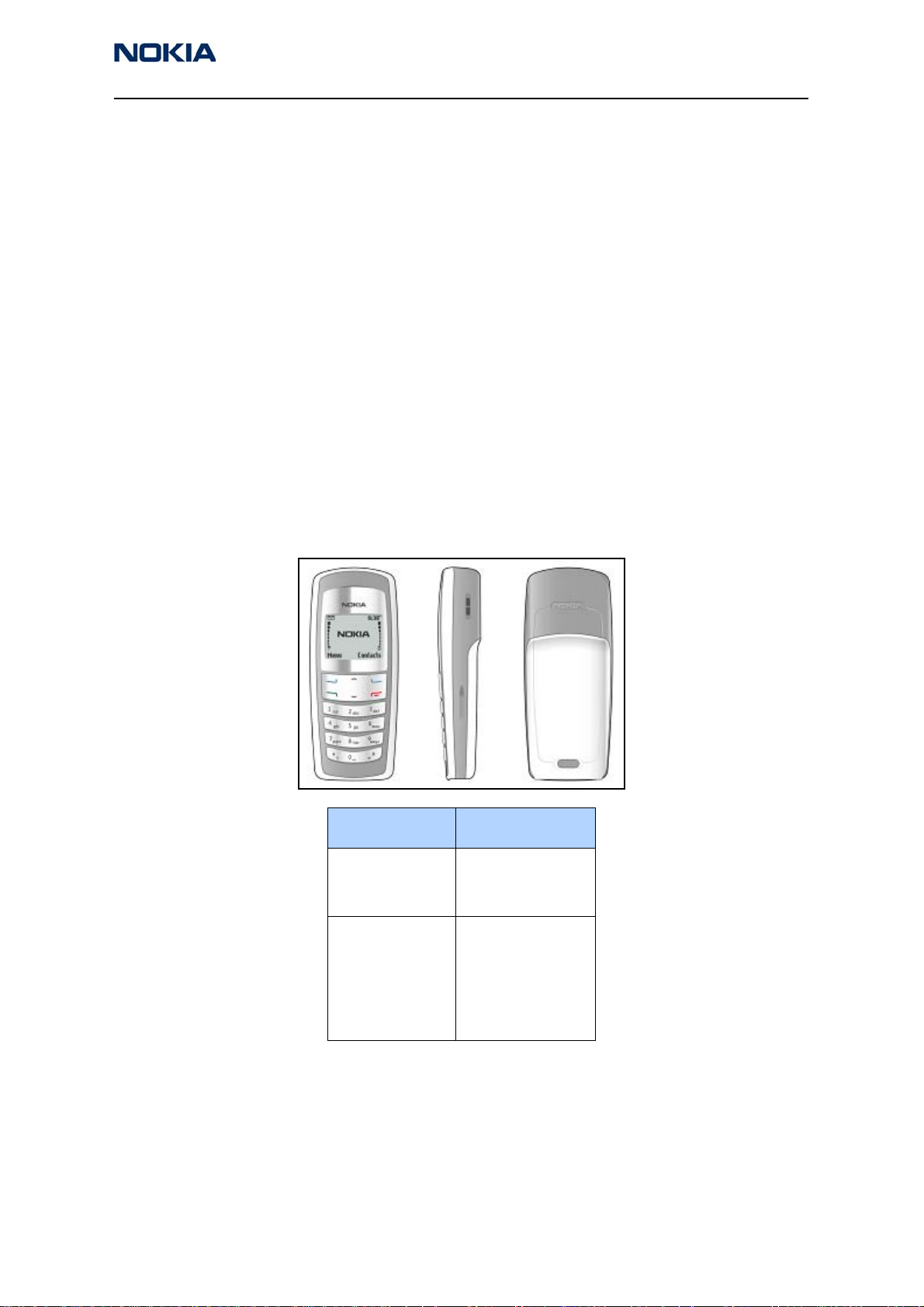
The Nokia 2115i/2116/2116i mobile terminal offers a CDMA trimode (800/1900MHz plus
AMPS) engine and includes the following features:
• Integrated, 2-way, hands-free speaker
• Flashlight
• Removable User Information Module (RUIM)
• 96 x 68 black and white display
• Internal vibra
• GPS for E-911 services (2115i and 2116i only)
• MIDI ring tone download and Qualcomm Code Excited Linear Prediction (QCELP)
decoding
• Changeable A-covers
• Openwave 4.1 browser
• Predictive text
Parameter Value and Unit
BL-6C
Talk time
Standby time
Dimensions:
Volume
Length
Width
Thickness
Weight
Up to 4.00 hours
Up to 212.00 hours
69 cc
102.4 mm
42.2 mm
21.5 mm
85 grams
Issue 1 03/2005 ©2005 Nokia Corporation Company Confidential Page 3
Page 14
2115i/2116/2116i (RH-66)
General Information
Sales Package
Name Type
Transceiver RH-66
Supported Accessories
Type Name
AC-1 Travel Charger
ACP-7 AC Travel Charger
ACP-12 Rapid Performance Charger
AD-5B Wireless Audio Adapter
BHF-3 Hands-free Headrest
CA-42 Data Cable
CK-7W Advanced Car Kit
CK-10 Basic Car Kit (no bluetooth)
DCV-14 Desk Stand
Battery BL-6C
(1070 mAh Li-Ion)
Charger ACP-7
BL-6C
HDB-4 Boom Headset
HDW-3 Wireless Headset
HF-2 Activity Hands Free
HF-3 Easy-to-use Hands Free
HS-3 Fashion Stereo Headset
HS-4W Wireless Boom Headset
HS-5 Headset
HS-10 Retractable Headset
HS-11W Basic Wireless Headset
LCH-12 Cigarette Lighter Charger
LPS-4 Inductive Loopset
MBC-15S Mobile Holder
Page 4 ©2005 Nokia Corporation Company Confidential Issue 1 03/2005
Page 15

Nokia Customer Care
2115i/2116/2116i (RH-66)
Mobile Terminals
Parts Lists and Exploded View
Issue 1 03/2005 Company Confidential ©2005 Nokia Corporation
Page 16

2115i/2116/2116i (RH-66)
Parts Lists and Exploded View
Contents Page
Exploded View ................................................................................................................................................. 3
Assembly Parts List .....................................................................................................................................3
2115i/2116i Parts List — Version 002 ...................................................................................................... 5
2116 Parts List — Version 001................................................................................................................. 19
Page 2 ©2005 Nokia Corporation Company Confidential Issue 1 03/2005
Page 17
2115i/2116/2116i (RH-66)
Nokia Customer Care Parts Lists and Exploded View
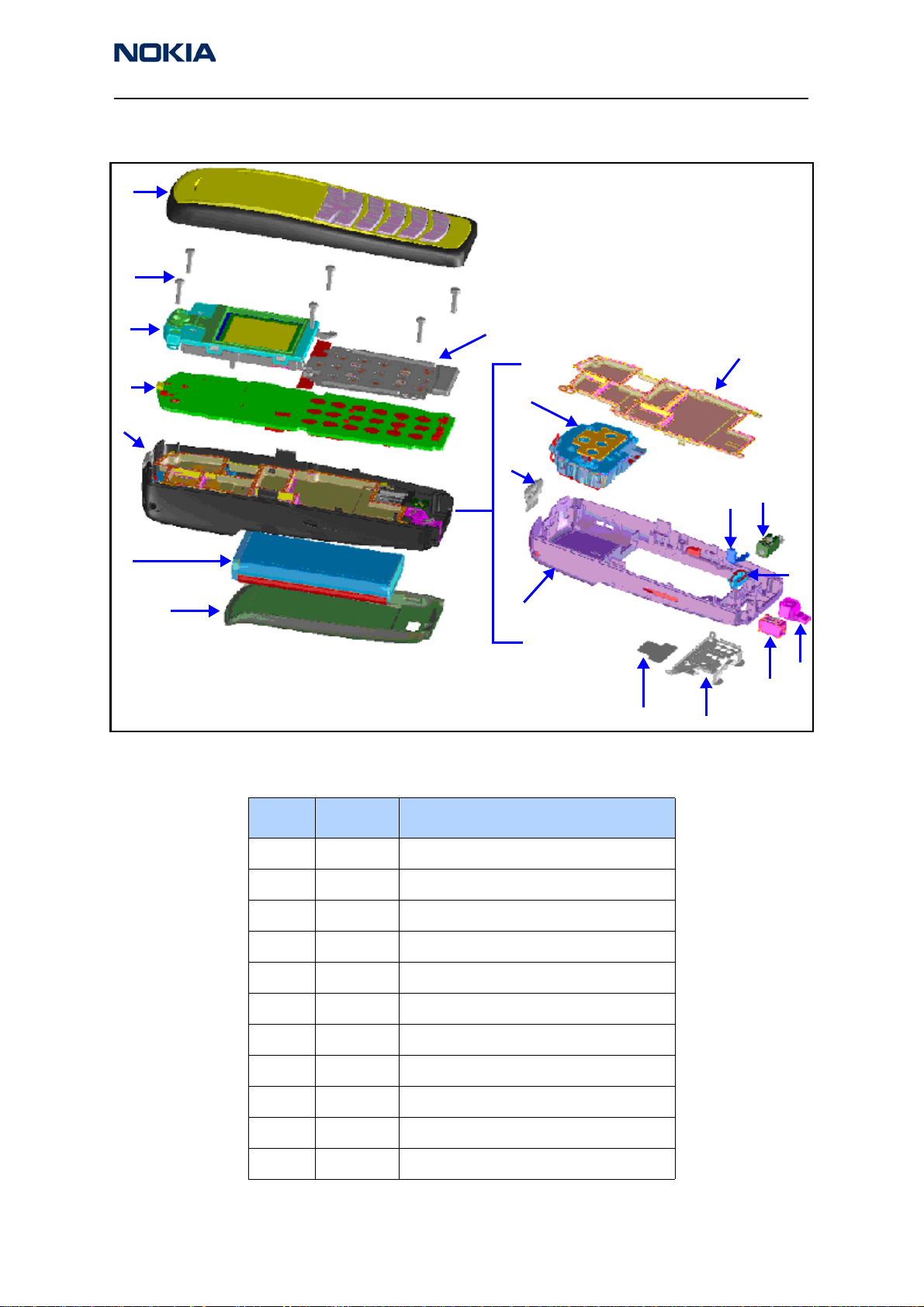
Exploded View
1
2
3
5
6
4
7
Assembly Parts List
8
6a
6b
6c
6f
6e
6g
6d
6h
6i
6k
6j
Item Qty Description
1 1 A-cover assembly
26 Screws
3 1 UI display assembly
4 1 Domesheet assembly
51 PWB
6 1 B-cover assembly
6a 1 PWB shield
6b 1 Antenna assembly
6c 1 Power button
6d 1 B-cover
6e 1 Release spring
Issue 1 03/2005 ©2005 Nokia Corporation Company Confidential Page 3
Page 18
2115i/2116/2116i (RH-66)
Parts Lists and Exploded View
Item Qty Description
6f 1 Vibra
6g 1 Release button
6h 1 Microphone
6i 1 DC jack
6j 1 SIM flap
6k 1 RUIM label
71 Battery
8 1 C-cover
Page 4 ©2005 Nokia Corporation Company Confidential Issue 1 03/2005
Page 19
2115i/2116/2116i (RH-66)
Nokia Customer Care Parts Lists and Exploded View
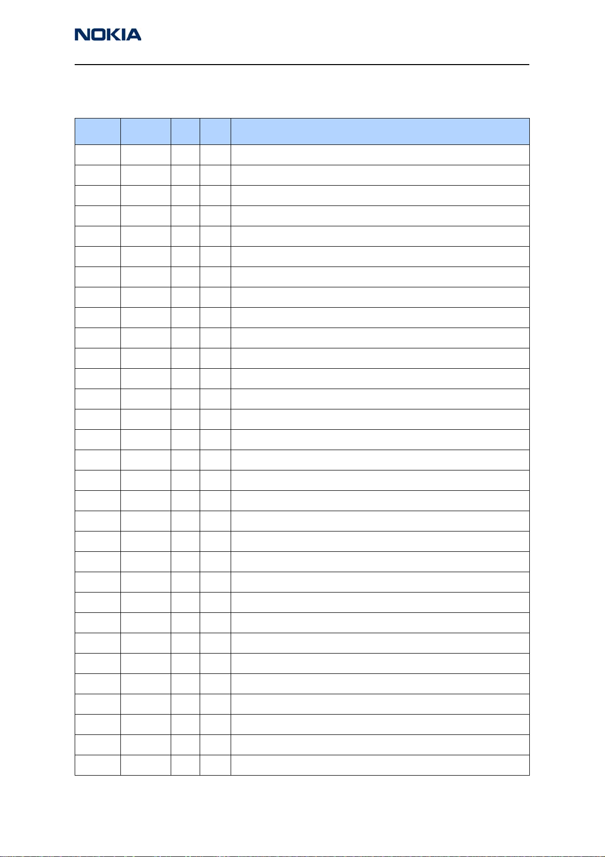
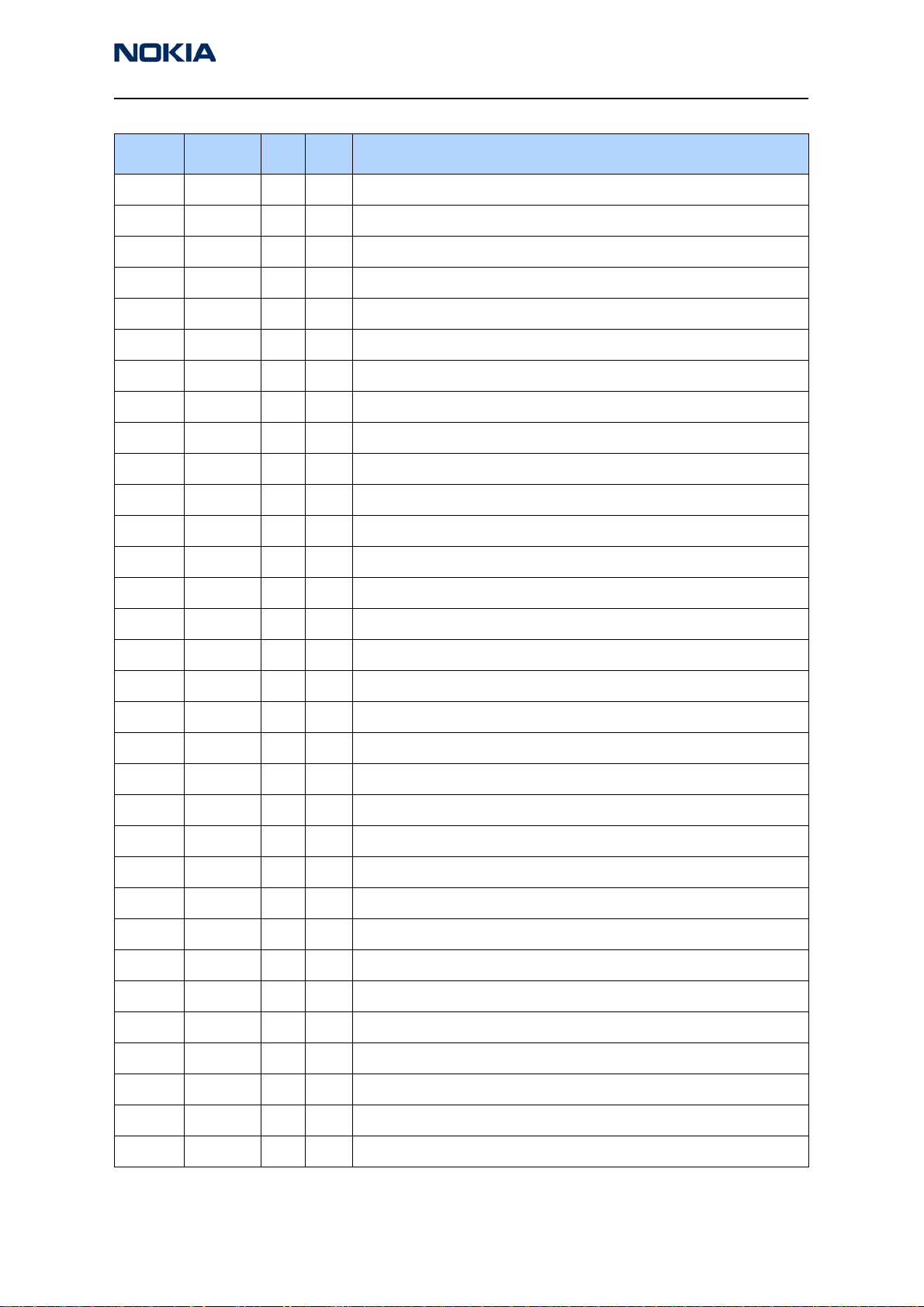
2115i/2116i Parts List — Version 002
Item Side X Y Description
B2200 Bottom P 2 CRYSTAL 32.768KHZ+-20PPM 12.5PF
C2000 Bottom P 4 CHIPCAP X7R 10N K 50V 0603
C2001 Bottom F 8 CHIPCAP NP0 47P J 50V 0402
C2002 Bottom G 8 CHIPCAP X5R 10U M 6V3 0805
C2003 Bottom F 7 CHIPCAP NP0 47P J 50V 0402
C2004 Top T 5 CHIPCAP X7R 1N0 J 50V 0402
C2006 Bottom L 7 CHIPCAP X5R 1U K 6V3 0603
C2007 Bottom L 7 CHIPCAP X5R 1U K 6V3 0603
C2008 Bottom L 8 CHIPCAP X7R 10N K 16V 0402
C2009 Bottom R 7 CHIPCAP NP0 22P J 50V 0402
C2010 Bottom R 7 CHIPCAP NP0 22P J 50V 0402
C2011 Bottom Q 3 CHIPCAP NP0 22P J 50V 0402
C2012 Top T 6 CHIPCAP X7R 3N3 J 50V 0402
C2013 Top T 6 CHIPCAP X7R 3N3 J 50V 0402
C2014 Top T 7 CHIPCAP X7R 3N3 J 50V 0402
C2015 Top T 7 CHIPCAP X7R 3N3 J 50V 0402
C2100 Bottom O 4 CHIPCAP NP0 39P J 50V 0402
C2101 Bottom O 3 CHIPCAP NP0 39P J 50V 0402
C2102 Bottom P 4 CHIP ARRAY X5R 2X100N Y 10V 0405
C2104 Bottom R 4 CHIPCAP NP0 47P J 50V 0402
C2105 Bottom Q 3 CHIPCAP X5R 100N M 16V 0402
C2106 Bottom O 3 CHIPCAP NP0 39P J 50V 0402
C2107 Bottom O 3 CHIPCAP NP0 39P J 50V 0402
C2108 Bottom P 3 CHIP ARRAY X5R 2X100N Y 10V 0405
C2109 Top T 7 CHIPCAP NP0 47P J 50V 0402
C2110 Top T 7 CHIPCAP X5R 100N M 16V 0402
C2111 Bottom Q 3 CHIPCAP X7R 2N2 J 50V 0402
C2112 Bottom Q 3 CHIPCAP X7R 22N K 16V 0402
C2113 Bottom Q 3 CHIPCAP X7R 22N K 16V 0402
C2114 Bottom P 2 CHIPCAP X5R 1U K 6V3 0603
C2116 Bottom P 3 CHIPCAP X5R 100N M 16V 0402
Issue 1 03/2005 ©2005 Nokia Corporation Company Confidential Page 5
Page 20

2115i/2116/2116i (RH-66)
Parts Lists and Exploded View
Item Side X Y Description
C2117 Bottom Q 2 CHIPCAP X5R 1U K 6V3 0603
C2118 Bottom P 3 CHIPCAP NP0 22P J 50V 0402
C2200 Bottom M 2 CHIPCAP X5R 1U K 6V3 0603
C2201 Bottom L 2 CHIPCAP X7R 10N K 16V 0402
C2202 Bottom N 2 CHIPCAP X5R 1U K 6V3 0603
C2203 Bottom N 2 CHIPCAP X5R 1U K 6V3 0603
C2204 Bottom O 4 CHIPCAP X5R 1U K 6V3 0603
C2205 Bottom L 2 CHIPCAP X5R 100N M 16V 0402
C2206 Bottom P 2 CHIPCAP NP0 18P J 50V 0402
C2207 Bottom P 2 CHIPCAP NP0 18P J 50V 0402
C2208 Bottom O 3 CHIPCAP X5R 1U K 6V3 0603
C2209 Bottom O 2 CHIPCAP X5R 1U K 6V3 0603
C2210 Bottom O 2 CHIPCAP X5R 1U K 6V3 0603
C2211 Bottom P 3 CHIPCAP X5R 1U K 6V3 0603
C2212 Bottom O 4 CHIPCAP X5R 1U K 6V3 0603
C2213 Bottom O 5 CHIPCAP X5R 1U K 6V3 0603
C2214 Bottom O 4 CHIPCAP X5R 1U K 6V3 0603
C2215 Bottom L 2 CHIPCAP X5R 10U M 6V3 0805
C2216 Bottom P 4 CHIPCAP X5R 100N M 16V 0402
C2217 Bottom P 5 CHIPCAP X5R 100N M 16V 0402
C2218 Bottom M 5 CHIPCAP X5R 100N M 16V 0402
C2219 Bottom M 5 CHIPCAP X5R 100N M 16V 0402
C2220 Bottom L 4 CHIPCAP X5R 1U K 6V3 0603
C2221 Bottom L 4 CHIPCAP X5R 100N M 16V 0402
C2222 Bottom L 4 CHIPCAP X5R 1U K 6V3 0603
C2223 Bottom L 4 CHIPCAP X5R 1U K 6V3 0603
C2224 Bottom L 4 CHIPCAP X5R 1U K 6V3 0603
C2225 Bottom M 2 CHIPCAP X5R 220N K 6.3V 0402
C2226 Bottom L 2 CHIPCAP X5R 1U K 6V3 0603
C2227 Bottom P 4 CHIPCAP X7R 10N K 16V 0402
C2228 Bottom P 4 CHIPCAP X7R 10N K 16V 0402
C2229 Bottom L 3 CHIPCAP X5R 1U K 6V3 0603
Page 6 ©2005 Nokia Corporation Company Confidential Issue 1 03/2005
Page 21
2115i/2116/2116i (RH-66)
Nokia Customer Care Parts Lists and Exploded View
Item Side X Y Description
C2230 Bottom L 3 CHIPCAP X5R 1U K 6V3 0603
C2231 Bottom L 3 CHIPCAP X5R 1U K 6V3 0603
C2232 Bottom L 2 CHIPCAP X5R 1U K 6V3 0603
C2233 Bottom L 3 CHIPCAP X5R 1U K 6V3 0603
C2234 Bottom L 3 CHIPCAP X5R 1U K 6V3 0603
C2235 Bottom L 3 CHIPCAP X5R 1U K 6V3 0603
C2236 Bottom L 4 CHIPCAP X5R 1U K 6V3 0603
C2237 Bottom L 4 CHIPCAP X5R 1U K 6V3 0603
C2300 Bottom M 8 CHIPCAP X5R 10U M 6V3 0805
C2301 Bottom L 8 CHIPCAP X5R 100N M 16V 0402
C2302 Bottom L 8 CHIPCAP X5R 10U M 6V3 0805
C2400 Top C 6 CHIPCAP X5R 100N M 16V 0402
C2401 Top C 6 CHIPCAP X5R 100N M 16V 0402
C2403 Top A 6 CHIPCAP NP0 47P J 50V 0402
C2404 Bottom N 8 CHIPCAP X5R 1U0 M 25V 1206
C2405 Bottom L 7 CHIPCAP X5R 100N M 16V 0402
C2406 Bottom B 5 CHIPCAP NP0 22P J 50V 0402
C2407 Bottom M 8 CHIPCAP X5R 1U K 6V3 0603
C2700 Bottom R 8 CHIPCAP X5R 100N M 16V 0402
C2880 Bottom P 5 CHIPCAP X5R 100N M 16V 0402
C2881 Bottom M 5 CHIPCAP X5R 100N M 16V 0402
C2882 Bottom M 7 CHIPCAP X5R 100N M 16V 0402
C2883 Bottom O 7 CHIPCAP X5R 100N M 16V 0402
C2884 Bottom M 5 CHIPCAP X5R 100N M 16V 0402
C2885 Bottom N 7 CHIPCAP X5R 100N M 16V 0402
C2900 Bottom O 7 CHIPCAP X7R 10N K 16V 0402
C2901 Bottom H 4 CHIPCAP X7R 10N K 16V 0402
C2902 Bottom O 7 CHIPCAP X7R 10N J 16V 0402
C2903 Bottom N 8 CHIPCAP X7R 1N0 K 50V 0402
C2904 Bottom O 8 CHIPCAP X7R 33N K 10V 0402
C2905 Bottom O 8 CHIPCAP X7R 10N J 16V 0402
C2906 Bottom O 8 CHIPCAP X7R 1N0 K 50V 0402
Issue 1 03/2005 ©2005 Nokia Corporation Company Confidential Page 7
Page 22
2115i/2116/2116i (RH-66)
Parts Lists and Exploded View
Item Side X Y Description
C2907 Bottom O 8 CHIPCAP X7R 33N K 10V 0402
C3000 Bottom L 5 CHIPCAP X7R 10N K 16V 0402
C3001 Bottom L 5 CHIPCAP X5R 100N M 16V 0402
C3002 Bottom M 5 CHIPCAP X7R 10N K 16V 0402
C6200 Bottom K 4 CHIPCAP X5R 100N M 16V 0402
C6201 Bottom K 4 CHIPCAP X5R 100N M 16V 0402
C6202 Bottom I 4 CHIPCAP X5R 100N M 16V 0402
C6203 Bottom I 4 CHIPCAP X5R 100N M 16V 0402
C6204 Bottom I 4 CHIPCAP X5R 100N M 16V 0402
C6205 Bottom K 4 CHIPCAP X5R 100N M 16V 0402
C6206 Bottom K 5 CHIPCAP X5R 100N M 16V 0402
C6207 Bottom L 7 CHIPCAP X5R 2U2 K 6V3 0603
C6208 Bottom K 8 CHIPCAP X7R 10N J 16V 0402
C6209 Bottom K 7 CHIPCAP X5R 2U2 K 6V3 0603
C6250 Bottom E 3 CHIPCAP X5R 100N M 16V 0402
C6251 Bottom E 3 CHIPCAP NP0 27P J 50V 0402
C6252 Bottom E 4 CHIPCAP X5R 1U K 6V3 0402
C6253 Bottom J 2 CHIPCAP X7R 10N K 16V 0402
C6254 Bottom F 4 CHIPCAP NP0 47P J 50V 0402
C6255 Bottom J 2 CHIPCAP NP0 10P J 50V 0402
C6256 Bottom F 3 CHIPCAP NP0 6P8 C 50V 0402
C6257 Bottom E 4 CHIPCAP NP0 10P J 50V 0402
C6258 Bottom I 3 CHIPCAP NP0 2P7 C 50V 0402
C6259 Bottom I 3 CHIPCAP NP0 15P J 50V 0402
C6260 Bottom D 2 CHIPCAP NP0 2P2 C 50V 0402
C6261 Bottom I 2 CHIPCAP X7R 10N J 16V 0402
C6262 Bottom J 2 CHIPCAP X7R 10N J 16V 0402
C6263 Bottom I 3 CHIPCAP X7R 10N J 16V 0402
C6264 Bottom J 2 CHIPCAP NP0 22P J 50V 0402
C6265 Bottom J 2 CHIPCAP NP0 22P J 50V 0402
C6266 Bottom I 3 CHIPCAP NP0 22P J 50V 0402
C6267 Bottom I 3 CHIPCAP X5R 100N M 16V 0402
Page 8 ©2005 Nokia Corporation Company Confidential Issue 1 03/2005
Page 23

2115i/2116/2116i (RH-66)
Nokia Customer Care Parts Lists and Exploded View
Item Side X Y Description
C6268 Bottom K 2 CHIPCAP NP0 22P J 50V 0402
C6269 Bottom K 3 CHIPCAP X5R 100N M 16V 0402
C7000 Bottom I 8 CHIPCAP X7R 10N J 16V 0402
C7001 Bottom J 7 CHIPCAP X5R 100N M 16V 0402
C7002 Bottom I 8 CHIPCAP X7R 10N J 16V 0402
C7003 Bottom I 7 CHIPCAP NP0 10P J 50V 0402
C7004 Bottom I 7 CHIPCAP NP0 1P2 C 50V 0402
C7005 Bottom I 7 CHIPCAP NP0 1P2 C 50V 0402
C7006 Bottom J 8 CHIPCAP NP0 3P3 C 50V 0402
C7007 Bottom J 8 CHIPCAP NP0 220P J 25V 0402
C7008 Bottom I 7 CHIPCAP X7R 10N J 16V 0402
C7009 Bottom I 7 CHIPCAP NP0 47P J 50V 0402
C7010 Bottom I 8 CHIPCAP NP0 10P J 50V 0402
C7012 Bottom I 8 CHIPCAP NP0 0P5 C 50V 0402
C7013 Bottom I 7 CHIPCAP NP0 0P5 C 50V 0402
C7014 Bottom J 8 CHIPCAP NP0 100P J 50V 0402
C7015 Bottom K 8 CHIPCAP NP0 2N2 J 16V 0603
C7016 Bottom J 8 CHIPCAP NP0 100P J 50V 0402
C7018 Bottom I 8 CHIPCAP X7R 10N J 16V 0402
C7019 Bottom I 8 CHIPCAP NP0 18P J 50V 0402
C7020 Bottom J 8 CHIPCAP X5R 1U K 6V3 0402
C7021 Bottom J 8 CHIPCAP NP0 18P J 50V 0402
C7022 Bottom K 8 CHIPCAP X7R 10N J 16V 0402
C7023 Bottom J 7 CHIPCAP NP0 33P J 50V 0402
C7024 Bottom J 7 CHIPCAP NP0 18P J 50V 0402
C7025 Bottom J 7 CHIPCAP NP0 33P J 50V 0402
C7027 Bottom I 8 CHIPCAP NP0 3P3 C 50V 0402
C7028 Bottom I 8 CHIPCAP NP0 3P3 C 50V 0402
C7029 Bottom J 8 CHIPCAP NP0 8P2 C 50V 0402
C7030 Bottom J 7 CHIPCAP NP0 8P2 C 50V 0402
C7100 Bottom H 6 CHIPCAP X7R 10N J 16V 0402
C7101 Bottom H 6 CHIPCAP X5R 330N K 10V 0603
Issue 1 03/2005 ©2005 Nokia Corporation Company Confidential Page 9
Page 24

2115i/2116/2116i (RH-66)
Parts Lists and Exploded View
Item Side X Y Description
C7102 Bottom H 6 CHIPCAP X7R 33N K 10V 0402
C7103 Bottom G 6 CHIPCAP NP0 33P J 50V 0402
C7104 Bottom G 6 CHIPCAP X7R 1N0 J 50V 0402
C7105 Bottom H 4 CHIPCAP X7R 10N K 16V 0402
C7106 Bottom H 5 CHIPCAP X7R 10N K 16V 0402
C7107 Bottom H 4 CHIPCAP X7R 10N K 16V 0402
C7108 Bottom G 5 CHIPCAP X7R 10N K 16V 0402
C7109 Bottom G 5 CHIPCAP X7R 10N K 16V 0402
C7110 Bottom H 4 CHIPCAP X7R 10N K 16V 0402
C7111 Bottom H 4 CHIPCAP X7R 10N K 16V 0402
C7112 Bottom F 5 CHIPCAP X7R 10N K 16V 0402
C7113 Bottom G 5 CHIPCAP X7R 10N K 16V 0402
C7160 Bottom C 5 CHIPCAP NP0 56P J 50V 0402
C7161 Bottom C 6 CHIPCAP NP0 2P2 C 50V 0402
C7162 Bottom C 4 CHIPCAP X5R 100N M 16V 0402
C7163 Bottom C 4 CHIPCAP NP0 10P J 50V 0402
C7164 Bottom C 4 CHIPCAP NP0 0P5 C 50V 0402
C7165 Bottom C 4 CHIPCAP NP0 1P5 C 50V 0402
C7166 Bottom D 6 CHIPCAP NP0 100P J 50V 0402
C7168 Bottom D 5 CHIPCAP NP0 5P6 C 50V 0402
C7169 Bottom F 5 CHIPCAP NP0 6P8 C 50V 0402
C7170 Bottom D 5 CHIPCAP X7R 1N0 J 50V 0402
C7171 Bottom E 5 CHIPCAP NP0 10P J 50V 0402
C7172 Bottom D 6 CHIPCAP NP0 3P9 C 50V 0402
C7173 Bottom D 5 CHIPCAP NP0 4P7 C 50V 0402
C7174 Bottom F 5 CHIPCAP NP0 6P8 C 50V 0402
C7175 Bottom C 3 CHIPCAP NP0 100P J 50V 0402
C7176 Bottom D 4 CHIPCAP X7R 3N3 J 50V 0402
C7177 Bottom D 4 CHIPCAP X7R 3N3 J 50V 0402
C7178 Bottom E 5 CHIPCAP X5R 100N M 16V 0402
C7179 Bottom D 4 CHIPCAP NP0 22P J 50V 0402
C7180 Bottom E 4 CHIPCAP NP0 2P2 C 50V 0402
Page 10 ©2005 Nokia Corporation Company Confidential Issue 1 03/2005
Page 25

2115i/2116/2116i (RH-66)
Nokia Customer Care Parts Lists and Exploded View
Item Side X Y Description
C7181 Bottom C 3 CHIPCAP NP0 100P J 50V 0402
C7182 Bottom G 4 CHIPCAP NP0 8P2 C 50V 0402
C7183 Bottom E 5 CHIPCAP NP0 100P J 50V 0402
C7184 Bottom C 5 CHIPCAP X7R 47N K 10V 0402
C7185 Bottom D 4 CHIPCAP NP0 12P J 50V 0402
C7186 Bottom C 4 CHIPCAP NP0 100P J 50V 0402
C7188 Bottom G 4 CHIPCAP NP0 8P2 C 50V 0402
C7200 Bottom L 4 CHIPCAP X5R 1U K 6V3 0402
C7203 Bottom L 4 CHIPCAP X7R 10N J 16V 0402
C7204 Bottom L 5 CHIPCAP X7R 1N0 J 50V 0402
C7206 Bottom L 5 CHIPCAP NP0 470P J 6V3 0402
C7207 Bottom L 4 CHIPCAP X7R 1N0 J 50V 0402
C7209 Bottom I 8 CHIPCAP NP0 470P J 6V3 0402
C7210 Bottom I 6 CHIPCAP NP0 470P J 6V3 0402
C7211 Bottom J 6 CHIPCAP X7R 470P J 50V 0402
C7212 Bottom I 5 CHIPCAP X7R 10N J 16V 0402
C7213 Bottom J 5 CHIPCAP X5R 100N M 16V 0402
C7214 Bottom J 6 CHIPCAP NP0 47P J 50V 0402
C7215 Bottom G 2 CHIPCAP X5R 1U K 6V3 0402
C7216 Bottom G 2 CHIPCAP X7R 10N J 16V 0402
C7218 Bottom J 6 CHIPCAP X7R 3N3 J 50V 0402
C7219 Bottom I 6 CHIPCAP X7R 1N0 J 50V 0402
C7220 Bottom I 5 CHIPCAP X7R 1N0 J 50V 0402
C7221 Bottom I 6 CHIPCAP X7R 33N K 10V 0402
C7222 Bottom I 6 CHIPCAP X7R 6N8 K 25V 0402
C7223 Bottom G 3 CHIPCAP NP0 1P8 C 50V 0402
C7224 Bottom H 4 CHIPCAP X5R 100N M 16V 0402
C7225 Bottom K 6 CHIPCAP X7R 10N J 16V 0402
C7226 Bottom K 5 CHIPCAP X5R 100N M 16V 0402
C7304 Bottom E 7 CHIPCAP X7R 1N0 J 50V 0402
C7306 Bottom E 8 CHIPCAP X7R 10N J 16V 0402
C7307 Bottom D 7 CHIPCAP NP0 15P J 50V 0402
Issue 1 03/2005 ©2005 Nokia Corporation Company Confidential Page 11
Page 26

2115i/2116/2116i (RH-66)
Parts Lists and Exploded View
Item Side X Y Description
C7308 Bottom E 9 CHIPCAP NP0 2P7 C 50V 0402
C7309 Bottom E 9 CHIPCAP X7R 1N0 J 50V 0402
C7310 Bottom E 7 CHIPCAP X5R 10U M 6V3 0805
C7311 Bottom C 8 CHIPCAP X7R 10N J 16V 0402
C7312 Bottom C 8 CHIPCAP X7R 3N3 J 50V 0402
C7313 Bottom C 8 CHIPCAP X7R 3N3 J 50V 0402
C7314 Bottom D 7 CHIPCAP NP0 47P J 50V 0402
C7315 Bottom D 6 CHIPCAP NP0 2P7 C 50V 0402
C7316 Bottom K 8 CHIPCAP X7R 1N0 J 50V 0402
C7317 Bottom E 7 CHIPCAP X7R 1N0 J 50V 0402
C7318 Bottom E 6 CHIPCAP NP0 100P J 50V 0402
C7319 Bottom D 6 CHIPCAP X7R 1N0 J 50V 0402
C7320 Bottom D 7 CHIPCAP X7R 1N0 J 50V 0402
C7321 Bottom E 7 CHIPCAP NP0 3P3 C 50V 0402
C7322 Bottom D 8 CHIPCAP NP0 2P2 C 50V 0402
D2200 Bottom N 4 UEMC 4.4 LF W/DOG ENA VCORE1V5
D2400 Bottom P 4 DIX2 BAV70W CC 70V .5A 4NS SOT323
D2401 Top Q 4 LED LW L283 WHITE 0603
D2402 Top Q 6 LED LW L283 WHITE 0603
D2403 Top N 4 LED LW L283 WHITE 0603
D2404 Top N 6 LED LW L283 WHITE 0603
D2405 Top A 5 LED CL430S-WF WHITE >500MCDD?20MA
D2800 Bottom N 6 UPP8M v4.2/v4.3/4.31 C027 12x12 UBGA144
D3000 Bottom L 6 FLASH 4MX16 1V8/1V8 VFBGA44 PBFREE
D6200 Bottom J 4 TWL5001 GPS BB ASIC V2.0 UBGA143
F2000 Top T 4 SM FUSE F 1.5A 32V ROHS-FREE 0603
G7200 Bottom L 5 VCTCXO 19.2MHZ +-2PPM 2.78V 2.2MA
G7201 Bottom H 3 UHF VCO 986-1034MHz/2040-2140MHz
L2000 Top T 4 FERR.BEAD 0R03 42R/100MHZ 3A 0805
L2001 Top T 6 FERRITE BEAD 600R 300MA 0.6R 0402
L2002 Top T 6 FERRITE BEAD 600R 300MA 0.6R 0402
L2003 Top T 6 CHIP BEAD ARRAY 2X1000R 0405
Page 12 ©2005 Nokia Corporation Company Confidential Issue 1 03/2005
Page 27

2115i/2116/2116i (RH-66)
Nokia Customer Care Parts Lists and Exploded View
Item Side X Y Description
L2004 Top T 7 CHIP BEAD ARRAY 2X1000R 0405
L2100 Bottom B 3 FERR.BEAD 240R/100M 0.4A 0R3 0402
L2101 Bottom B 3 FERR.BEAD 240R/100M 0.4A 0R3 0402
L2300 Bottom L 8 FERR.BEAD 0R03 42R/100MHZ 3A 0805
L2301 Bottom M 8 CHOKE 10UH M 0.49A 3.0X2.8X1.2MM
L2400 Bottom M 7 FERR.BEAD 0R03 42R/100MHZ 3A 0805
L2401 Bottom N 8 CHOKE 22U M 1R4 0.33A 3.3X3.3X1.5
L6250 Bottom E 4 CHIP COIL 15N J Q30/800MHZ 0402
L6251 Bottom F 3 CHIP COIL 3N9 +-0N3 Q28/800M 0402
L6252 Bottom I 3 CHIP COIL 8N2 J Q28/800MHZ 0402
L6253 Bottom D 2 CHIP COIL 15N J Q30/800MHZ 0402
L7000 Bottom I 7 CHIP COIL 27N J Q27/800MHZ 0402
L7001 Bottom I 7 CHIP COIL 33N J Q23/800MHZ 0402
L7002 Bottom I 7 CHIP COIL 27N J Q27/800MHZ 0402
L7003 Bottom I 8 CHIP COIL 6N8 J Q27/800MHZ 0402
L7004 Bottom I 7 CHIP COIL 12N J Q31/800MHZ 0402
L7005 Bottom I 8 CHIP COIL 6N8 J Q27/800MHZ 0402
L7101 Bottom G 6 CHIP COIL 33NH J Q12/100MHZ 0603
L7160 Bottom C 5 CHIP COIL 15N J Q30/800MHZ 0402
L7161 Bottom C 4 CHIP COIL 3N3 +-0N3 Q28/800M 0402
L7162 Bottom C 5 CHIP COIL 6N2 J Q20/250MHZ 0402
L7163 Bottom C 5 CHIP COIL 19N J Q25/250MHZ 0402
L7164 Bottom D 5 CHIP COIL 220N J Q8/50MHZ 0603
L7165 Bottom F 5 CHIP COIL 120N J Q16/100MHZ 0603
L7166 Bottom D 3 CHIP COIL 12N J Q31/800MHZ 0402
L7167 Bottom D 5 CHIP COIL 180N J Q13/100MHZ 0603
L7168 Bottom F 5 CHIP COIL 220N J Q8/50MHZ 0603
L7169 Bottom F 6 CHIP COIL 120N J Q16/100MHZ 0603
L7170 Bottom D 5 CHIP COIL 82N +-0N3 Q17/300M 0402
L7171 Bottom D 4 CHIP COIL 18N J Q29/800MHZ 0402
L7172 Bottom D 5 CHIP COIL 3N3 +-0N3 Q28/800M 0402
L7173 Bottom D 5 CHIP COIL 82N +-0N3 Q17/300M 0402
Issue 1 03/2005 ©2005 Nokia Corporation Company Confidential Page 13
Page 28

2115i/2116/2116i (RH-66)
Parts Lists and Exploded View
Item Side X Y Description
L7174 Bottom E 5 CHIP COIL 120N J Q16/100MHZ 0603
L7175 Bottom D 5 CHIP COIL 15N J Q30/800MHZ 0402
L7176 Bottom G 4 CHIP COIL 120N J Q16/100MHZ 0603
L7177 Bottom G 4 CHIP COIL 120N J Q16/100MHZ 0603
L7178 Bottom F 6 CHIP COIL 220N J Q8/50MHZ 0603
L7179 Bottom G 4 CHIP COIL 100N J Q12/100MHZ 0603
L7200 Bottom G 3 CHIP COIL 3N3 +-0N3 Q28/800M 0402
L7302 Bottom C 7 DIR.COUPLER 1850-1910MHZ 1.6X0.8
L7304 Bottom C 6 CHIP COIL 10N J Q30/800MHZ 0402
L7305 Bottom E 7 CHIP COIL 3N3 +-0N3 Q28/800M 0402
L7306 Bottom C 7 DIR.COUPLER 824-849MHZ 1.6X0.8MM
L7308 Bottom D 8 CHIP COIL 3N9 +-0N3 Q28/800M 0402
L7310 Bottom K 8 CHIP COIL 27N J Q27/800MHZ 0402
N2000 Bottom L 8 VREG LP3985ITLX-2.8 NOPB USMD5
N2100 Bottom P 3 AF AMP 0.4W LM4890/NCP2890 PBFREE
N2300 Bottom M 8 DC/DC CONV LM2708H-1.35V/1.05V
N2400 Bottom N 8 DC/DC CONV TK65600 USMD8
N6200 Bottom L 8 VREG LP3985ITLX-2.8 NOPB USMD5
N6250 Bottom K 3 TCXO 16.368MHZ+-1.5PPM 2.8V GPS
N6251 Bottom J 3 GPS RX TRF5101 PG2.1 PBGA-49
N7000 Bottom J 8 JUPITER D4 PMB3365G VQFN-40
N7100 Bottom H 5 BATMAN RF RX ASIC STB7102FTR
N7160 Bottom D 5 LNA/MIXER/DOWNCNTR ALFRED VQFN-24
N7200 Bottom J 6 1XPLL/SYNTH 2.5GHZ(LMX2310U)MLF20
N7300 Bottom C 8 ASIP STPAC01F2 CDMA PWR DET BGA-8
N7301 Bottom E 7 PW AMP RF3449 CDMA800 LFM
N7302 Bottom E 8 PW AMP RF3448 CDMA1900
R2000 Bottom O 8 NTC RES 0W1 47K J B 4050+-3% 0402
R2001 Bottom L 8 CHIPRES 0W06 100K J 0402
R2002 Bottom Q 3 CHIPRES 0W06 100K J 0402
R2003 Bottom Q 3 RES NETWORK 0W06 2X47R J 0404
R2004 Bottom R 7 RES NETWORK 0W06 2X47R J 0404
Page 14 ©2005 Nokia Corporation Company Confidential Issue 1 03/2005
Page 29

2115i/2116/2116i (RH-66)
Nokia Customer Care Parts Lists and Exploded View
Item Side X Y Description
R2006 Bottom R 7 RES NETWORK 0W06 2X47R J 0404
R2007 Bottom R 8 CHIPRES 0W06 220K J 0402
R2008 Top T 6 VARISTOR ARRAY 2XVWM16V VC50 0405
R2009 Top T 8 VARISTOR ARRAY 2XVWM16V VC50 0405
R2100 Bottom B 5 RES NETWORK 0W06 2X5R6 J 0404
R2101 Bottom O 4 RES NETWORK 0W06 2X1K0 J 0404
R2102 Bottom P 4 CHIPRES 0W06 47K J 0402
R2103 Bottom Q 4 RES NETWORK 0W06 2X1K0 J 0404
R2104 Bottom R 3 RES NETWORK 0W06 2X1K0 J 0404
R2105 Bottom B 5 VARISTOR ARRAY 2XVWM16V VC50 0405
R2106 Bottom O 3 RES NETWORK 0W06 2X1K0 J 0404
R2107 Bottom P 3 CHIPRES 0W06 47K J 0402
R2108 Top T 7 RES NETWORK 0W06 2X1K0 J 0404
R2109 Top T 7 RES NETWORK 0W06 2X1K0 J 0404
R2110 Top T 8 RES NETWORK 0W06 2X5R6 J 0404
R2111 Bottom Q 3 CHIPRES 0W06 470R J 0402
R2112 Bottom Q 3 CHIPRES 0W06 5K6 J 0402
R2113 Bottom Q 3 CHIPRES 0W06 180K F 200PPM 0402
R2200 Bottom M 2 CHIPRES 0W25 0R22 J 0805
R2201 Bottom P 5 RES NETWORK 0W03 4X100K J 0804
R2202 Bottom P 4 RES NETWORK 0W06 2X4K7 J 0404
R2205 Bottom R 7 CHIPRES 0W06 10K J 0402
R2403 Bottom Q 4 CHIPRES 0W06 33R J 0402
R2404 Bottom Q 4 CHIPRES 0W06 68R J 0402
R2405 Bottom Q 4 CHIPRES 0W06 68R J 0402
R2407 Bottom Q 4 CHIPRES 0W06 150R J 0603
R2408 Bottom Q 4 CHIPRES 0W06 150R J 0603
R2409 Bottom A 5 CHIPRES 0W06 4K7 J 0402
R2410 Bottom Q 4 CHIPRES 0W06 3K3 J 0402
R2411 Bottom N 8 CHIPRES 0W06 22K F 200PPM 0402
R2412 Bottom N 8 CHIPRES 0W06 1K3 F 250PPM 0402
R2700 Bottom R 7 ASIP SIM INTERFACE ** PB-FREE **
Issue 1 03/2005 ©2005 Nokia Corporation Company Confidential Page 15
Page 30

2115i/2116/2116i (RH-66)
Parts Lists and Exploded View
Item Side X Y Description
R2900 Bottom O 7 CHIPRES 0W06 4K7 J 0402
R2901 Bottom O 7 CHIPRES 0W06 1K0 J 0402
R2902 Bottom O 7 CHIPRES 0W06 4K7 J 0402
R2903 Bottom O 8 CHIPRES 0W06 1K0 J 0402
R2904 Bottom O 8 CHIPRES 0W06 4K7 J 0402
R3000 Bottom M 5 CHIPRES 0W06 4K7 J 0402
R6202 Bottom I 4 CHIPRES 0W06 100K J 0402
R6203 Bottom L 8 CHIPRES JUMPER 0R0 0402
R6204 Bottom I 4 CHIPRES 0W06 100K J 0402
R6250 Bottom E 3 CHIPRES 0W06 120R J 0402
R6251 Bottom E 3 CHIPRES 0W06 22K J 0402
R6252 Bottom E 4 CHIPRES 0W06 10R J 0402
R6253 Bottom F 3 CHIPRES 0W06 150R J 0402
R7000 Bottom I 8 CHIPRES JUMPER 0R0 0402
R7001 Bottom J 8 CHIPRES 0W06 10K J 0402
R7002 Bottom J 8 CHIPRES 0W06 27K J 0402
R7003 Bottom I 7 CHIPRES 0W06 12K J 0402
R7004 Bottom K 7 CHIPRES JUMPER 0R0 0402
R7005 Bottom J 7 CHIPRES JUMPER 0R0 0402
R7006 Bottom K 7 CHIPRES JUMPER 0R0 0402
R7007 Bottom J 7 CHIPRES JUMPER 0R0 0402
R7008 Bottom H 8 CHIPRES JUMPER 0R0 0402
R7009 Bottom K 7 CHIPRES 0W06 150R J 0402
R7010 Bottom K 7 CHIPRES 0W06 100R J 0402
R7011 Bottom K 7 CHIPRES 0W06 33K J 0402
R7012 Bottom J 7 CHIPRES 0W06 2K2 J 0402
R7013 Bottom J 7 CHIPRES 0W06 39K J 0402
R7100 Bottom G 6 CHIPRES 0W06 1K0 J 0402
R7101 Bottom H 5 CHIPRES 0W06 470R J 0402
R7102 Bottom G 6 CHIPRES 0W06 4K7 J 0402
R7103 Bottom H 4 CHIPRES 0W06 8K2 J 0402
R7104 Bottom H 5 CHIPRES 0W06 27K J 0402
Page 16 ©2005 Nokia Corporation Company Confidential Issue 1 03/2005
Page 31

2115i/2116/2116i (RH-66)
Nokia Customer Care Parts Lists and Exploded View
Item Side X Y Description
R7160 Bottom C 4 CHIPRES 0W06 4R3 J 0402
R7161 Bottom C 3 CHIPRES 0W06 47K J 0402
R7162 Bottom D 4 CHIPRES 0W06 82R J 0402
R7163 Bottom C 3 CHIPRES 0W06 47K J 0402
R7164 Bottom D 4 CHIPRES 0W06 4R3 J 0402
R7165 Bottom C 4 CHIPRES 0W06 47K J 0402
R7200 Bottom L 4 CHIPRES 0W06 10R J 0402
R7204 Bottom L 5 CHIPRES 0W06 1K0 J 0402
R7205 Bottom L 4 CHIPRES 0W06 10K J 0402
R7208 Bottom J 5 CHIPRES 0W06 10R J 0402
R7209 Bottom G 2 CHIPRES JUMPER 0R0 0402
R7210 Bottom G 3 CHIPRES 0W06 150R J 0402
R7211 Bottom I 6 CHIPRES 0W06 10K J 0402
R7212 Bottom I 5 CHIPRES 0W06 10K J 0402
R7213 Bottom J 6 CHIPRES 0W06 3K9 J 0402
R7215 Bottom H 4 CHIPRES 0W06 2K2 J 0402
R7216 Bottom K 6 CHIPRES 0W06 10R J 0402
R7300 Bottom E 8 CHIPRES JUMPER 0R0 0402
R7301 Bottom C 7 CHIPRES 0W06 56R J 0402
R7302 Bottom C 7 CHIPRES JUMPER 0R0 0402
R7304 Bottom H 8 CHIPRES 0W06 100R J 0402
R7305 Bottom I 8 CHIPRES 0W06 100R J 0402
R7307 Bottom C 6 CHIPRES 0W06 56R J 0402
R7308 Bottom E 7 CHIPRES JUMPER 0R0 0402
R7309 Bottom F 8 NTC RES 0W1 47K J B 4050+-3% 0402
R7330 Bottom E 4 CHIPRES JUMPER 0R0 0402
S2418 Bottom A 5 SM TACT SW SIDE TRAVEL 0.2 MM
V2000 Top T 5 TVS DI 1PMT16AT3 16V 175W PWRMITE
V2400 Bottom R 5 TRX2 UMT1/PUMT1 P40V100MA SOT363
V2401 Bottom Q 5 TRX2 UMT1/PUMT1 P40V100MA SOT363
V2402 Bottom Q 5 TRX2 UMT1/PUMT1 P40V100MA SOT363
V2403 Bottom P 4 TR DTC143ZE N RBE4K7/47K 0A1 SC75
Issue 1 03/2005 ©2005 Nokia Corporation Company Confidential Page 17
Page 32

2115i/2116/2116i (RH-66)
Parts Lists and Exploded View
Item Side X Y Description
V2404 Bottom R 4 TR DTC143ZE N RBE4K7/47K 0A1 SC75
V2900 Bottom O 8 TRX2+RX2 UMH3N N50V0.1A4K7 SOT363
V6250 Bottom F 3 TR BFP620 LNA 65GHZ NF.7DB SOT343
V7100 Bottom G 5 CAP.DI BBY57-02W 1/4 16/4P SOD523
X2000 Bottom G 7 SM BATTERY CONN 3POL SPR 12V 2A
X2001 Bottom T 6 SM SYSTEM CONNECTOR 14POL
X2400 Top B 7 SM CONN 2X5F P0.5 PWB/PWB
X2700 Bottom Q 7 SM SIM CONNECTOR 6POL P2.54
X6250 Bottom F 2 SM COAX CONN+SW F 50R 250V 6GHZ
X7300 Top B 4 SM COAX CONN+SW F 50R 250V 6GHZ
X8000 Top A 9 MODULE ID COMPONENT 2.8X1.8X0.3
Z2005 Top T 6 ASIP 4XESD *** PB-FREE *** BGA5
Z2400 Bottom R 6 ASIP KEYBOARD INTERFACE *PB-FREE*
Z6250 Bottom D 4 CER FILT 1575.42+-4MHZ 3.5X3.5X2
Z6251 Bottom I 2 SAW FILT 1575+-2MHZ/2DB 2.6X2.1X1
Z7000 Bottom H 7 SAW FILT 836.5+-12.5MHZ 2X1.6
Z7001 Bottom H 7 SAW FILT 1880+-30MHZ/3.5DB 2X1.6
Z7160 Bottom C 6 SAW FILT 881.5+-12.5MHZ/2.5 2X1.6
Z7161 Bottom D 4 SAW FILT 1960+-30MHZ/3.2DB 2X1.6
Z7162 Bottom E 5 XTAL FILT 128.1MHZ/4DB 3X3X1
Z7163 Bottom F 4 SAW FILT 128.1MHZ 7X5X1.48
Z7300 Bottom B 6 DIPL 824-894/1850-1990MHZ 2X1.25
Z7301 Bottom D 8 DUPL 1850-1910MHz 5X5
Z7302 Bottom D 7 DUPL 824-849/869-894MHZ 3.8X3.8X1.5
Page 18 ©2005 Nokia Corporation Company Confidential Issue 1 03/2005
Page 33

2115i/2116/2116i (RH-66)
Nokia Customer Care Parts Lists and Exploded View
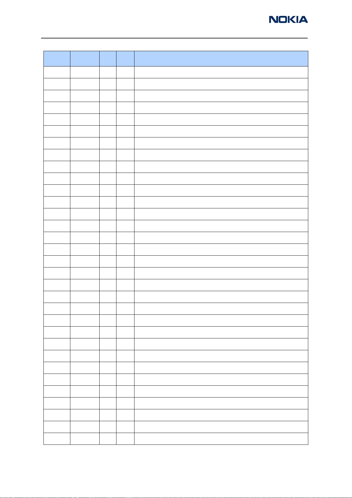
2116 Parts List — Version 001
Item Side X Y Description
B2200 Bottom P 2 CRYSTAL 32.768KHZ+-20PPM 12.5PF
C2000 Bottom P 4 CHIPCAP X7R 10N K 50V 0603
C2001 Bottom F 8 CHIPCAP NP0 47P J 50V 0402
C2002 Bottom G 8 CHIPCAP X5R 10U M 6V3 0805
C2003 Bottom F 7 CHIPCAP NP0 47P J 50V 0402
C2004 Top T 5 CHIPCAP X7R 1N0 J 50V 0402
C2006 Bottom L 7 CHIPCAP X5R 1U K 6V3 0603
C2007 Bottom L 7 CHIPCAP X5R 1U K 6V3 0603
C2008 Bottom L 8 CHIPCAP X7R 10N K 16V 0402
C2009 Bottom R 7 CHIPCAP NP0 22P J 50V 0402
C2010 Bottom R 7 CHIPCAP NP0 22P J 50V 0402
C2011 Bottom Q 3 CHIPCAP NP0 22P J 50V 0402
C2012 Top T 6 CHIPCAP X7R 3N3 J 50V 0402
C2013 Top T 6 CHIPCAP X7R 3N3 J 50V 0402
C2014 Top T 7 CHIPCAP X7R 3N3 J 50V 0402
C2015 Top T 7 CHIPCAP X7R 3N3 J 50V 0402
C2100 Bottom O 4 CHIPCAP NP0 39P J 50V 0402
C2101 Bottom O 3 CHIPCAP NP0 39P J 50V 0402
C2102 Bottom P 4 CHIP ARRAY X5R 2X100N Y 10V 0405
C2104 Bottom R 4 CHIPCAP NP0 47P J 50V 0402
C2105 Bottom Q 3 CHIPCAP X5R 100N M 16V 0402
C2106 Bottom O 3 CHIPCAP NP0 39P J 50V 0402
C2107 Bottom O 3 CHIPCAP NP0 39P J 50V 0402
C2108 Bottom P 3 CHIP ARRAY X5R 2X100N Y 10V 0405
C2109 Top T 7 CHIPCAP NP0 47P J 50V 0402
C2110 Top T 7 CHIPCAP X5R 100N M 16V 0402
C2111 Bottom Q 3 CHIPCAP X7R 2N2 J 50V 0402
C2112 Bottom Q 3 CHIPCAP X7R 22N K 16V 0402
C2113 Bottom Q 3 CHIPCAP X7R 22N K 16V 0402
C2114 Bottom P 2 CHIPCAP X5R 1U K 6V3 0603
C2116 Bottom P 3 CHIPCAP X5R 100N M 16V 0402
Issue 1 03/2005 ©2005 Nokia Corporation Company Confidential Page 19
Page 34

2115i/2116/2116i (RH-66)
Parts Lists and Exploded View
Item Side X Y Description
C2117 Bottom Q 2 CHIPCAP X5R 1U K 6V3 0603
C2118 Bottom P 3 CHIPCAP NP0 22P J 50V 0402
C2200 Bottom M 2 CHIPCAP X5R 1U K 6V3 0603
C2201 Bottom L 2 CHIPCAP X7R 10N K 16V 0402
C2202 Bottom N 2 CHIPCAP X5R 1U K 6V3 0603
C2203 Bottom N 2 CHIPCAP X5R 1U K 6V3 0603
C2204 Bottom O 4 CHIPCAP X5R 1U K 6V3 0603
C2205 Bottom L 2 CHIPCAP X5R 100N M 16V 0402
C2206 Bottom P 2 CHIPCAP NP0 18P J 50V 0402
C2207 Bottom P 2 CHIPCAP NP0 18P J 50V 0402
C2208 Bottom O 3 CHIPCAP X5R 1U K 6V3 0603
C2209 Bottom O 2 CHIPCAP X5R 1U K 6V3 0603
C2210 Bottom O 2 CHIPCAP X5R 1U K 6V3 0603
C2211 Bottom P 3 CHIPCAP X5R 1U K 6V3 0603
C2212 Bottom O 4 CHIPCAP X5R 1U K 6V3 0603
C2213 Bottom O 5 CHIPCAP X5R 1U K 6V3 0603
C2214 Bottom O 4 CHIPCAP X5R 1U K 6V3 0603
C2215 Bottom L 2 CHIPCAP X5R 10U M 6V3 0805
C2216 Bottom P 4 CHIPCAP X5R 100N M 16V 0402
C2217 Bottom P 5 CHIPCAP X5R 100N M 16V 0402
C2218 Bottom M 5 CHIPCAP X5R 100N M 16V 0402
C2219 Bottom M 5 CHIPCAP X5R 100N M 16V 0402
C2220 Bottom L 4 CHIPCAP X5R 1U K 6V3 0603
C2221 Bottom L 4 CHIPCAP X5R 100N M 16V 0402
C2222 Bottom L 4 CHIPCAP X5R 1U K 6V3 0603
C2223 Bottom L 4 CHIPCAP X5R 1U K 6V3 0603
C2224 Bottom L 4 CHIPCAP X5R 1U K 6V3 0603
C2225 Bottom M 2 CHIPCAP X5R 220N K 6.3V 0402
C2226 Bottom L 2 CHIPCAP X5R 1U K 6V3 0603
C2227 Bottom P 4 CHIPCAP X7R 10N K 16V 0402
C2228 Bottom P 4 CHIPCAP X7R 10N K 16V 0402
C2229 Bottom L 3 CHIPCAP X5R 1U K 6V3 0603
Page 20 ©2005 Nokia Corporation Company Confidential Issue 1 03/2005
Page 35

2115i/2116/2116i (RH-66)
Nokia Customer Care Parts Lists and Exploded View
Item Side X Y Description
C2230 Bottom L 3 CHIPCAP X5R 1U K 6V3 0603
C2231 Bottom L 3 CHIPCAP X5R 1U K 6V3 0603
C2232 Bottom L 2 CHIPCAP X5R 1U K 6V3 0603
C2233 Bottom L 3 CHIPCAP X5R 1U K 6V3 0603
C2234 Bottom L 3 CHIPCAP X5R 1U K 6V3 0603
C2235 Bottom L 3 CHIPCAP X5R 1U K 6V3 0603
C2236 Bottom L 4 CHIPCAP X5R 1U K 6V3 0603
C2237 Bottom L 4 CHIPCAP X5R 1U K 6V3 0603
C2300 Bottom M 8 CHIPCAP X5R 10U M 6V3 0805
C2301 Bottom L 8 CHIPCAP X5R 100N M 16V 0402
C2302 Bottom L 8 CHIPCAP X5R 10U M 6V3 0805
C2400 Top C 6 CHIPCAP X5R 100N M 16V 0402
C2401 Top C 6 CHIPCAP X5R 100N M 16V 0402
C2403 Top A 6 CHIPCAP NP0 47P J 50V 0402
C2404 Bottom N 8 CHIPCAP X5R 1U0 M 25V 1206
C2405 Bottom L 7 CHIPCAP X5R 100N M 16V 0402
C2406 Bottom B 5 CHIPCAP NP0 22P J 50V 0402
C2407 Bottom M 8 CHIPCAP X5R 1U K 6V3 0603
C2700 Bottom R 8 CHIPCAP X5R 100N M 16V 0402
C2880 Bottom P 5 CHIPCAP X5R 100N M 16V 0402
C2881 Bottom M 5 CHIPCAP X5R 100N M 16V 0402
C2882 Bottom M 7 CHIPCAP X5R 100N M 16V 0402
C2883 Bottom O 7 CHIPCAP X5R 100N M 16V 0402
C2884 Bottom M 5 CHIPCAP X5R 100N M 16V 0402
C2885 Bottom N 7 CHIPCAP X5R 100N M 16V 0402
C2900 Bottom O 7 CHIPCAP X7R 10N K 16V 0402
C2901 Bottom H 4 CHIPCAP X7R 10N K 16V 0402
C2902 Bottom O 7 CHIPCAP X7R 10N J 16V 0402
C2903 Bottom N 8 CHIPCAP X7R 1N0 K 50V 0402
C2904 Bottom O 8 CHIPCAP X7R 33N K 10V 0402
C2905 Bottom O 8 CHIPCAP X7R 10N J 16V 0402
C2906 Bottom O 8 CHIPCAP X7R 1N0 K 50V 0402
Issue 1 03/2005 ©2005 Nokia Corporation Company Confidential Page 21
Page 36

2115i/2116/2116i (RH-66)
Parts Lists and Exploded View
Item Side X Y Description
C2907 Bottom O 8 CHIPCAP X7R 33N K 10V 0402
C3000 Bottom L 5 CHIPCAP X7R 10N K 16V 0402
C3001 Bottom L 5 CHIPCAP X5R 100N M 16V 0402
C3002 Bottom M 5 CHIPCAP X7R 10N K 16V 0402
C6260 Bottom D 2 CHIPCAP NP0 2P2 C 50V 0402
C7000 Bottom I 8 CHIPCAP X7R 10N J 16V 0402
C7001 Bottom J 7 CHIPCAP X5R 100N M 16V 0402
C7002 Bottom I 8 CHIPCAP X7R 10N J 16V 0402
C7003 Bottom I 7 CHIPCAP NP0 10P J 50V 0402
C7004 Bottom I 7 CHIPCAP NP0 1P2 C 50V 0402
C7005 Bottom I 7 CHIPCAP NP0 1P2 C 50V 0402
C7006 Bottom J 8 CHIPCAP NP0 3P3 C 50V 0402
C7007 Bottom J 8 CHIPCAP NP0 220P J 25V 0402
C7008 Bottom I 7 CHIPCAP X7R 10N J 16V 0402
C7009 Bottom I 7 CHIPCAP NP0 47P J 50V 0402
C7010 Bottom I 8 CHIPCAP NP0 10P J 50V 0402
C7012 Bottom I 8 CHIPCAP NP0 0P5 C 50V 0402
C7013 Bottom I 7 CHIPCAP NP0 0P5 C 50V 0402
C7014 Bottom J 8 CHIPCAP NP0 100P J 50V 0402
C7015 Bottom K 8 CHIPCAP NP0 2N2 J 16V 0603
C7016 Bottom J 8 CHIPCAP NP0 100P J 50V 0402
C7018 Bottom I 8 CHIPCAP X7R 10N J 16V 0402
C7019 Bottom I 8 CHIPCAP NP0 18P J 50V 0402
C7020 Bottom J 8 CHIPCAP X5R 1U K 6V3 0402
C7021 Bottom J 8 CHIPCAP NP0 18P J 50V 0402
C7022 Bottom K 8 CHIPCAP X7R 10N J 16V 0402
C7023 Bottom J 7 CHIPCAP NP0 33P J 50V 0402
C7024 Bottom J 7 CHIPCAP NP0 18P J 50V 0402
C7025 Bottom J 7 CHIPCAP NP0 33P J 50V 0402
C7027 Bottom I 8 CHIPCAP NP0 3P3 C 50V 0402
C7028 Bottom I 8 CHIPCAP NP0 3P3 C 50V 0402
C7029 Bottom J 8 CHIPCAP NP0 8P2 C 50V 0402
Page 22 ©2005 Nokia Corporation Company Confidential Issue 1 03/2005
Page 37

2115i/2116/2116i (RH-66)
Nokia Customer Care Parts Lists and Exploded View
Item Side X Y Description
C7030 Bottom J 7 CHIPCAP NP0 8P2 C 50V 0402
C7100 Bottom H 6 CHIPCAP X7R 10N J 16V 0402
C7101 Bottom H 6 CHIPCAP X5R 330N K 10V 0603
C7102 Bottom H 6 CHIPCAP X7R 33N K 10V 0402
C7103 Bottom G 6 CHIPCAP NP0 33P J 50V 0402
C7104 Bottom G 6 CHIPCAP X7R 1N0 J 50V 0402
C7105 Bottom H 4 CHIPCAP X7R 10N K 16V 0402
C7106 Bottom H 5 CHIPCAP X7R 10N K 16V 0402
C7107 Bottom H 4 CHIPCAP X7R 10N K 16V 0402
C7108 Bottom G 5 CHIPCAP X7R 10N K 16V 0402
C7109 Bottom G 5 CHIPCAP X7R 10N K 16V 0402
C7110 Bottom H 4 CHIPCAP X7R 10N K 16V 0402
C7111 Bottom H 4 CHIPCAP X7R 10N K 16V 0402
C7112 Bottom F 5 CHIPCAP X7R 10N K 16V 0402
C7113 Bottom G 5 CHIPCAP X7R 10N K 16V 0402
C7160 Bottom C 5 CHIPCAP NP0 56P J 50V 0402
C7161 Bottom C 6 CHIPCAP NP0 2P2 C 50V 0402
C7162 Bottom C 4 CHIPCAP X5R 100N M 16V 0402
C7163 Bottom C 4 CHIPCAP NP0 10P J 50V 0402
C7164 Bottom C 4 CHIPCAP NP0 0P5 C 50V 0402
C7165 Bottom C 4 CHIPCAP NP0 1P5 C 50V 0402
C7166 Bottom D 6 CHIPCAP NP0 100P J 50V 0402
C7168 Bottom D 5 CHIPCAP NP0 5P6 C 50V 0402
C7169 Bottom F 5 CHIPCAP NP0 6P8 C 50V 0402
C7170 Bottom D 5 CHIPCAP X7R 1N0 J 50V 0402
C7171 Bottom E 5 CHIPCAP NP0 10P J 50V 0402
C7172 Bottom D 6 CHIPCAP NP0 3P9 C 50V 0402
C7173 Bottom D 5 CHIPCAP NP0 4P7 C 50V 0402
C7174 Bottom F 5 CHIPCAP NP0 6P8 C 50V 0402
C7175 Bottom C 3 CHIPCAP NP0 100P J 50V 0402
C7176 Bottom D 4 CHIPCAP X7R 3N3 J 50V 0402
C7177 Bottom D 4 CHIPCAP X7R 3N3 J 50V 0402
Issue 1 03/2005 ©2005 Nokia Corporation Company Confidential Page 23
Page 38

2115i/2116/2116i (RH-66)
Parts Lists and Exploded View
Item Side X Y Description
C7178 Bottom E 5 CHIPCAP X5R 100N M 16V 0402
C7179 Bottom D 4 CHIPCAP NP0 22P J 50V 0402
C7180 Bottom E 4 CHIPCAP NP0 2P2 C 50V 0402
C7181 Bottom C 3 CHIPCAP NP0 100P J 50V 0402
C7182 Bottom G 4 CHIPCAP NP0 8P2 C 50V 0402
C7183 Bottom E 5 CHIPCAP NP0 100P J 50V 0402
C7184 Bottom C 5 CHIPCAP X7R 47N K 10V 0402
C7185 Bottom D 4 CHIPCAP NP0 12P J 50V 0402
C7186 Bottom C 4 CHIPCAP NP0 100P J 50V 0402
C7188 Bottom G 4 CHIPCAP NP0 8P2 C 50V 0402
C7200 Bottom L 4 CHIPCAP X5R 1U K 6V3 0402
C7203 Bottom L 4 CHIPCAP X7R 10N J 16V 0402
C7204 Bottom L 5 CHIPCAP X7R 1N0 J 50V 0402
C7207 Bottom L 4 CHIPCAP X7R 1N0 J 50V 0402
C7209 Bottom I 8 CHIPCAP NP0 470P J 6V3 0402
C7210 Bottom I 6 CHIPCAP NP0 470P J 6V3 0402
C7211 Bottom J 6 CHIPCAP X7R 470P J 50V 0402
C7212 Bottom I 5 CHIPCAP X7R 10N J 16V 0402
C7213 Bottom J 5 CHIPCAP X5R 100N M 16V 0402
C7214 Bottom J 6 CHIPCAP NP0 47P J 50V 0402
C7215 Bottom G 2 CHIPCAP X5R 1U K 6V3 0402
C7216 Bottom G 2 CHIPCAP X7R 10N J 16V 0402
C7218 Bottom J 6 CHIPCAP X7R 3N3 J 50V 0402
C7219 Bottom I 6 CHIPCAP X7R 1N0 J 50V 0402
C7220 Bottom I 5 CHIPCAP X7R 1N0 J 50V 0402
C7221 Bottom I 6 CHIPCAP X7R 33N K 10V 0402
C7222 Bottom I 6 CHIPCAP X7R 6N8 K 25V 0402
C7223 Bottom G 3 CHIPCAP NP0 1P8 C 50V 0402
C7224 Bottom H 4 CHIPCAP X5R 100N M 16V 0402
C7225 Bottom K 6 CHIPCAP X7R 10N J 16V 0402
C7226 Bottom K 5 CHIPCAP X5R 100N M 16V 0402
C7304 Bottom E 7 CHIPCAP X7R 1N0 J 50V 0402
Page 24 ©2005 Nokia Corporation Company Confidential Issue 1 03/2005
Page 39

2115i/2116/2116i (RH-66)
Nokia Customer Care Parts Lists and Exploded View
Item Side X Y Description
C7306 Bottom E 8 CHIPCAP X7R 10N J 16V 0402
C7307 Bottom D 7 CHIPCAP NP0 15P J 50V 0402
C7308 Bottom E 9 CHIPCAP NP0 2P7 C 50V 0402
C7309 Bottom E 9 CHIPCAP X7R 1N0 J 50V 0402
C7310 Bottom E 7 CHIPCAP X5R 10U M 6V3 0805
C7311 Bottom C 8 CHIPCAP X7R 10N J 16V 0402
C7312 Bottom C 8 CHIPCAP X7R 3N3 J 50V 0402
C7313 Bottom C 8 CHIPCAP X7R 3N3 J 50V 0402
C7314 Bottom D 7 CHIPCAP NP0 47P J 50V 0402
C7315 Bottom D 6 CHIPCAP NP0 2P7 C 50V 0402
C7316 Bottom K 8 CHIPCAP X7R 1N0 J 50V 0402
C7317 Bottom E 7 CHIPCAP X7R 1N0 J 50V 0402
C7318 Bottom E 6 CHIPCAP NP0 100P J 50V 0402
C7319 Bottom D 6 CHIPCAP X7R 1N0 J 50V 0402
C7320 Bottom D 7 CHIPCAP X7R 1N0 J 50V 0402
C7321 Bottom E 7 CHIPCAP NP0 3P3 C 50V 0402
C7322 Bottom D 8 CHIPCAP NP0 2P2 C 50V 0402
D2200 Bottom N 4 UEMC 4.4 LF W/DOG ENA VCORE1V5
D2400 Bottom P 4 DIX2 BAV70W CC 70V .5A 4NS SOT323
D2401 Top Q 4 LED LW L283 WHITE 0603
D2402 Top Q 6 LED LW L283 WHITE 0603
D2403 Top N 4 LED LW L283 WHITE 0603
D2404 Top N 6 LED LW L283 WHITE 0603
D2405 Top A 5 LED CL430S-WF WHITE >500MCDD?20MA
D2800 Bottom N 6 UPP8M v4.2/v4.3/4.31 C027 12x12 UBGA144
D3000 Bottom L 6 FLASH 4MX16 1V8/1V8 VFBGA44 PBFREE
F2000 Top T 4 SM FUSE F 1.5A 32V ROHS-FREE 0603
G7200 Bottom L 5 VCTCXO 19.2MHZ +-2PPM 2.78V 2.2MA
G7201 Bottom H 3 UHF VCO 986-1034MHz/2040-2140MHz
L2000 Top T 4 FERR.BEAD 0R03 42R/100MHZ 3A 0805
L2001 Top T 6 FERRITE BEAD 600R 300MA 0.6R 0402
L2002 Top T 6 FERRITE BEAD 600R 300MA 0.6R 0402
Issue 1 03/2005 ©2005 Nokia Corporation Company Confidential Page 25
Page 40

2115i/2116/2116i (RH-66)
Parts Lists and Exploded View
Item Side X Y Description
L2003 Top T 6 CHIP BEAD ARRAY 2X1000R 0405
L2004 Top T 7 CHIP BEAD ARRAY 2X1000R 0405
L2100 Bottom B 3 FERR.BEAD 240R/100M 0.4A 0R3 0402
L2101 Bottom B 3 FERR.BEAD 240R/100M 0.4A 0R3 0402
L2300 Bottom L 8 FERR.BEAD 0R03 42R/100MHZ 3A 0805
L2301 Bottom M 8 CHOKE 10UH M 0.49A 3.0X2.8X1.2MM
L2400 Bottom M 7 FERR.BEAD 0R03 42R/100MHZ 3A 0805
L2401 Bottom N 8 CHOKE 22U M 1R4 0.33A 3.3X3.3X1.5
L6253 Bottom D 2 CHIP COIL 15N J Q30/800MHZ 0402
L7000 Bottom I 7 CHIP COIL 27N J Q27/800MHZ 0402
L7001 Bottom I 7 CHIP COIL 33N J Q23/800MHZ 0402
L7002 Bottom I 7 CHIP COIL 27N J Q27/800MHZ 0402
L7003 Bottom I 8 CHIP COIL 6N8 J Q27/800MHZ 0402
L7004 Bottom I 7 CHIP COIL 12N J Q31/800MHZ 0402
L7005 Bottom I 8 CHIP COIL 6N8 J Q27/800MHZ 0402
L7101 Bottom G 6 CHIP COIL 33NH J Q12/100MHZ 0603
L7160 Bottom C 5 CHIP COIL 15N J Q30/800MHZ 0402
L7161 Bottom C 4 CHIP COIL 3N3 +-0N3 Q28/800M 0402
L7162 Bottom C 5 CHIP COIL 6N2 J Q20/250MHZ 0402
L7163 Bottom C 5 CHIP COIL 19N J Q25/250MHZ 0402
L7164 Bottom D 5 CHIP COIL 220N J Q8/50MHZ 0603
L7165 Bottom F 5 CHIP COIL 120N J Q16/100MHZ 0603
L7166 Bottom D 3 CHIP COIL 12N J Q31/800MHZ 0402
L7167 Bottom D 5 CHIP COIL 180N J Q13/100MHZ 0603
L7168 Bottom F 5 CHIP COIL 220N J Q8/50MHZ 0603
L7169 Bottom F 6 CHIP COIL 120N J Q16/100MHZ 0603
L7170 Bottom D 5 CHIP COIL 82N +-0N3 Q17/300M 0402
L7171 Bottom D 4 CHIP COIL 18N J Q29/800MHZ 0402
L7172 Bottom D 5 CHIP COIL 3N3 +-0N3 Q28/800M 0402
L7173 Bottom D 5 CHIP COIL 82N +-0N3 Q17/300M 0402
L7174 Bottom E 5 CHIP COIL 120N J Q16/100MHZ 0603
L7175 Bottom D 5 CHIP COIL 15N J Q30/800MHZ 0402
Page 26 ©2005 Nokia Corporation Company Confidential Issue 1 03/2005
Page 41

2115i/2116/2116i (RH-66)
Nokia Customer Care Parts Lists and Exploded View
Item Side X Y Description
L7176 Bottom G 4 CHIP COIL 120N J Q16/100MHZ 0603
L7177 Bottom G 4 CHIP COIL 120N J Q16/100MHZ 0603
L7178 Bottom F 6 CHIP COIL 220N J Q8/50MHZ 0603
L7179 Bottom G 4 CHIP COIL 100N J Q12/100MHZ 0603
L7200 Bottom G 3 CHIP COIL 3N3 +-0N3 Q28/800M 0402
L7302 Bottom C 7 DIR.COUPLER 1850-1910MHZ 1.6X0.8
L7304 Bottom C 6 CHIP COIL 10N J Q30/800MHZ 0402
L7305 Bottom E 7 CHIP COIL 3N3 +-0N3 Q28/800M 0402
L7306 Bottom C 7 DIR.COUPLER 824-849MHZ 1.6X0.8MM
L7308 Bottom D 8 CHIP COIL 3N9 +-0N3 Q28/800M 0402
L7310 Bottom K 8 CHIP COIL 27N J Q27/800MHZ 0402
N2000 Bottom L 8 VREG LP3985ITLX-2.8 NOPB USMD5
N2100 Bottom P 3 AF AMP 0.4W LM4890/NCP2890 PBFREE
N2300 Bottom M 8 DC/DC CONV LM2708H-1.35V/1.05V
N2400 Bottom N 8 DC/DC CONV TK65600 USMD8
N7000 Bottom J 8 JUPITER D4 PMB3365G VQFN-40
N7100 Bottom H 5 BATMAN RF RX ASIC STB7102FTR
N7160 Bottom D 5 LNA/MIXER/DOWNCNTR ALFRED VQFN-24
N7200 Bottom J 6 1XPLL/SYNTH 2.5GHZ(LMX2310U)MLF20
N7300 Bottom C 8 ASIP STPAC01F2 CDMA PWR DET BGA-8
N7301 Bottom E 7 PW AMP RF3449 CDMA800 LFM
N7302 Bottom E 8 PW AMP RF3448 CDMA1900
R2000 Bottom O 8 NTC RES 0W1 47K J B 4050+-3% 0402
R2001 Bottom L 8 CHIPRES 0W06 100K J 0402
R2002 Bottom Q 3 CHIPRES 0W06 100K J 0402
R2003 Bottom Q 3 RES NETWORK 0W06 2X47R J 0404
R2004 Bottom R 7 RES NETWORK 0W06 2X47R J 0404
R2006 Bottom R 7 RES NETWORK 0W06 2X47R J 0404
R2007 Bottom R 8 CHIPRES 0W06 220K J 0402
R2008 Top T 6 VARISTOR ARRAY 2XVWM16V VC50 0405
R2009 Top T 8 VARISTOR ARRAY 2XVWM16V VC50 0405
R2100 Bottom B 5 RES NETWORK 0W06 2X5R6 J 0404
Issue 1 03/2005 ©2005 Nokia Corporation Company Confidential Page 27
Page 42

2115i/2116/2116i (RH-66)
Parts Lists and Exploded View
Item Side X Y Description
R2101 Bottom O 4 RES NETWORK 0W06 2X1K0 J 0404
R2102 Bottom P 4 CHIPRES 0W06 47K J 0402
R2103 Bottom Q 4 RES NETWORK 0W06 2X1K0 J 0404
R2104 Bottom R 3 RES NETWORK 0W06 2X1K0 J 0404
R2105 Bottom B 5 VARISTOR ARRAY 2XVWM16V VC50 0405
R2106 Bottom O 3 RES NETWORK 0W06 2X1K0 J 0404
R2107 Bottom P 3 CHIPRES 0W06 47K J 0402
R2108 Top T 7 RES NETWORK 0W06 2X1K0 J 0404
R2109 Top T 7 RES NETWORK 0W06 2X1K0 J 0404
R2110 Top T 8 RES NETWORK 0W06 2X5R6 J 0404
R2111 Bottom Q 3 CHIPRES 0W06 470R J 0402
R2112 Bottom Q 3 CHIPRES 0W06 5K6 J 0402
R2113 Bottom Q 3 CHIPRES 0W06 180K F 200PPM 0402
R2200 Bottom M 2 CHIPRES 0W25 0R22 J 0805
R2201 Bottom P 5 RES NETWORK 0W03 4X100K J 0804
R2202 Bottom P 4 RES NETWORK 0W06 2X4K7 J 0404
R2205 Bottom R 7 CHIPRES 0W06 10K J 0402
R2403 Bottom Q 4 CHIPRES 0W06 33R J 0402
R2404 Bottom Q 4 CHIPRES 0W06 68R J 0402
R2405 Bottom Q 4 CHIPRES 0W06 68R J 0402
R2407 Bottom Q 4 CHIPRES 0W06 150R J 0603
R2408 Bottom Q 4 CHIPRES 0W06 150R J 0603
R2409 Bottom A 5 CHIPRES 0W06 4K7 J 0402
R2410 Bottom Q 4 CHIPRES 0W06 3K3 J 0402
R2411 Bottom N 8 CHIPRES 0W06 22K F 200PPM 0402
R2412 Bottom N 8 CHIPRES 0W06 1K3 F 250PPM 0402
R2700 Bottom R 7 ASIP SIM INTERFACE ** PB-FREE **
R2900 Bottom O 7 CHIPRES 0W06 4K7 J 0402
R2901 Bottom O 7 CHIPRES 0W06 1K0 J 0402
R2902 Bottom O 7 CHIPRES 0W06 4K7 J 0402
R2903 Bottom O 8 CHIPRES 0W06 1K0 J 0402
R2904 Bottom O 8 CHIPRES 0W06 4K7 J 0402
Page 28 ©2005 Nokia Corporation Company Confidential Issue 1 03/2005
Page 43

2115i/2116/2116i (RH-66)
Nokia Customer Care Parts Lists and Exploded View
Item Side X Y Description
R3000 Bottom M 5 CHIPRES 0W06 4K7 J 0402
R7000 Bottom I 8 CHIPRES JUMPER 0R0 0402
R7001 Bottom J 8 CHIPRES 0W06 10K J 0402
R7002 Bottom J 8 CHIPRES 0W06 27K J 0402
R7003 Bottom I 7 CHIPRES 0W06 12K J 0402
R7004 Bottom K 7 CHIPRES JUMPER 0R0 0402
R7005 Bottom J 7 CHIPRES JUMPER 0R0 0402
R7006 Bottom K 7 CHIPRES JUMPER 0R0 0402
R7007 Bottom J 7 CHIPRES JUMPER 0R0 0402
R7008 Bottom H 8 CHIPRES JUMPER 0R0 0402
R7009 Bottom K 7 CHIPRES 0W06 150R J 0402
R7010 Bottom K 7 CHIPRES 0W06 100R J 0402
R7011 Bottom K 7 CHIPRES 0W06 33K J 0402
R7012 Bottom J 7 CHIPRES 0W06 2K2 J 0402
R7013 Bottom J 7 CHIPRES 0W06 39K J 0402
R7100 Bottom G 6 CHIPRES 0W06 1K0 J 0402
R7101 Bottom H 5 CHIPRES 0W06 470R J 0402
R7102 Bottom G 6 CHIPRES 0W06 4K7 J 0402
R7103 Bottom H 4 CHIPRES 0W06 8K2 J 0402
R7104 Bottom H 5 CHIPRES 0W06 27K J 0402
R7160 Bottom C 4 CHIPRES 0W06 4R3 J 0402
R7161 Bottom C 3 CHIPRES 0W06 47K J 0402
R7162 Bottom D 4 CHIPRES 0W06 82R J 0402
R7163 Bottom C 3 CHIPRES 0W06 47K J 0402
R7164 Bottom D 4 CHIPRES 0W06 4R3 J 0402
R7165 Bottom C 4 CHIPRES 0W06 47K J 0402
R7200 Bottom L 4 CHIPRES 0W06 10R J 0402
R7204 Bottom L 5 CHIPRES 0W06 1K0 J 0402
R7205 Bottom L 4 CHIPRES 0W06 10K J 0402
R7208 Bottom J 5 CHIPRES 0W06 10R J 0402
R7209 Bottom G 2 CHIPRES JUMPER 0R0 0402
R7210 Bottom G 3 CHIPRES 0W06 150R J 0402
Issue 1 03/2005 ©2005 Nokia Corporation Company Confidential Page 29
Page 44

2115i/2116/2116i (RH-66)
Parts Lists and Exploded View
Item Side X Y Description
R7211 Bottom I 6 CHIPRES 0W06 10K J 0402
R7212 Bottom I 5 CHIPRES 0W06 10K J 0402
R7213 Bottom J 6 CHIPRES 0W06 3K9 J 0402
R7215 Bottom H 4 CHIPRES 0W06 2K2 J 0402
R7216 Bottom K 6 CHIPRES 0W06 10R J 0402
R7300 Bottom E 8 CHIPRES JUMPER 0R0 0402
R7301 Bottom C 7 CHIPRES 0W06 56R J 0402
R7302 Bottom C 7 CHIPRES JUMPER 0R0 0402
R7304 Bottom H 8 CHIPRES 0W06 100R J 0402
R7305 Bottom I 8 CHIPRES 0W06 100R J 0402
R7307 Bottom C 6 CHIPRES 0W06 56R J 0402
R7308 Bottom E 7 CHIPRES JUMPER 0R0 0402
R7309 Bottom F 8 NTC RES 0W1 47K J B 4050+-3% 0402
R7330 Bottom E 4 CHIPRES JUMPER 0R0 0402
S2418 Bottom A 5 SM TACT SW SIDE TRAVEL 0.2 MM
V2000 Top T 5 TVS DI 1PMT16AT3 16V 175W PWRMITE
V2400 Bottom R 5 TRX2 UMT1/PUMT1 P40V100MA SOT363
V2401 Bottom Q 5 TRX2 UMT1/PUMT1 P40V100MA SOT363
V2402 Bottom Q 5 TRX2 UMT1/PUMT1 P40V100MA SOT363
V2403 Bottom P 4 TR DTC143ZE N RBE4K7/47K 0A1 SC75
V2404 Bottom R 4 TR DTC143ZE N RBE4K7/47K 0A1 SC75
V2900 Bottom O 8 TRX2+RX2 UMH3N N50V0.1A4K7 SOT363
V7100 Bottom G 5 CAP.DI BBY57-02W 1/4 16/4P SOD523
X2000 Bottom G 7 SM BATTERY CONN 3POL SPR 12V 2A
X2001 Bottom T 6 SM SYSTEM CONNECTOR 14POL
X2400 Top B 7 SM CONN 2X5F P0.5 PWB/PWB
X2700 Bottom Q 7 SM SIM CONNECTOR 6POL P2.54
X7300 Top B 4 SM COAX CONN+SW F 50R 250V 6GHZ
X8000 Top A 9 MODULE ID COMPONENT 2.8X1.8X0.3
Z2005 Top T 6 ASIP 4XESD *** PB-FREE *** BGA5
Z2400 Bottom R 6 ASIP KEYBOARD INTERFACE *PB-FREE*
Z7000 Bottom H 7 SAW FILT 836.5+-12.5MHZ 2X1.6
Page 30 ©2005 Nokia Corporation Company Confidential Issue 1 03/2005
Page 45

2115i/2116/2116i (RH-66)
Nokia Customer Care Parts Lists and Exploded View
Item Side X Y Description
Z7001 Bottom H 7 SAW FILT 1880+-30MHZ/3.5DB 2X1.6
Z7160 Bottom C 6 SAW FILT 881.5+-12.5MHZ/2.5 2X1.6
Z7161 Bottom D 4 SAW FILT 1960+-30MHZ/3.2DB 2X1.6
Z7162 Bottom E 5 XTAL FILT 128.1MHZ/4DB 3X3X1
Z7163 Bottom F 4 SAW FILT 128.1MHZ 7X5X1.48
Z7300 Bottom B 6 DIPL 824-894/1850-1990MHZ 2X1.25
Z7301 Bottom D 8 DUPL 1850-1910MHz 5X5
Z7302 Bottom D 7 DUPL 824-849/869-894MHZ 3.8X3.8X1.5
Issue 1 03/2005 ©2005 Nokia Corporation Company Confidential Page 31
Page 46

2115i/2116/2116i (RH-66)
Parts Lists and Exploded View Nokia Customer Care
This page intentionally left blank.
Page 32 ©2005 Nokia Corporation Company Confidential Issue 1 03/2005
Page 47

Nokia Customer Care
2115i/2116/2116i (RH-66)
Mobile Terminals
Service Software Instructions
Issue 1 03/2005 Company Confidential ©2005 Nokia Corporation
Page 48

2115i/2116/2116i (RH-66)
Service Software Instructions
Contents Page
Introduction ..................................................................................................................................................... 3
Hardware and Operating System Requirements ................................................................................3
Phoenix Service Software............................................................................................................................. 4
Before You Begin .........................................................................................................................................4
Creating a Phoenix Connection ...............................................................................................................4
Scanning for a Product ..............................................................................................................................6
Using Components ......................................................................................................................................6
Using Profiles ................................................................................................................................................6
Diego Service Software................................................................................................................................. 7
Before You Begin .........................................................................................................................................7
Initial Session with Diego and FLS-4S Dongle ....................................................................................7
Scanning for a Product ..............................................................................................................................8
Using Components ......................................................................................................................................8
Uninstalling Service Software..................................................................................................................... 9
Page 2 ©2005 Nokia Corporation Company Confidential Issue 1 03/2005
Page 49

2115i/2116/2116i (RH-66)
Nokia Customer Care Service Software Instructions
Introduction
You must obtain software support bundles (SSBs) to load software upgrade files to
customer-specific mobile terminal models. The SSBs are InstallShield executable
packages. Double-click on the package, and the software installs automatically. No
rebooting of the computer is required.
These bundles are created by Nokia Customer Care and made available by Nokia After
Market Services (AMS) on the Partners Web Page for your applicable region:
• Americas = https://americas.partners.nokia.com
•APAC = https://apac.partners.nokia.com
• China = https://china.partners.nokia.com
•EMEA = https://trade.online.nokia.com or https://europe.partners.nokia.com
The Web pages are password controlled. If you have not registered as a user, contact
Nokia Central Service.
Hardware and Operating System Requirements
Table 1: Minimum Hardware Requirements
Hardware Minimum Value
Processor 700 MHz
RAM 256 MB
Disk space needed 100-200 MB
Interface ports Parallel or USB (dongle-
dependent)
Table 2: Supported Operating System Requirements
Operating System Notes
Windows 2000 Professional version
Windows XP
Issue 1 03/2005 ©2005 Nokia Corporation Company Confidential Page 3
Page 50

2115i/2116/2116i (RH-66)
Service Software Instructions
Phoenix Service Software
Before You Begin
Before you installing Phoenix, ensure the following:
• Uninstall any previous versions of Phoenix that exist on the machine. See
"Uninstalling Service Software" on page 9.
• If the computer supports administrator rights, ensure that access is enabled for
the user performing the Phoenix installation.
• Phoenix requires the complete Phoenix installation package, which is around
30 MB.
• You MUST have a Nokia dongle installed on the computer prior to beginning the
software installation. The dongle is attached to the parallel port for PKD dongles,
or an FLS-4S dongle is attached to either the parallel port or the Universal Serial
Bus (USB) port (if the computer supports USB).
• Custom installation is only recommended for experienced users.
• After installation, reboot the computer prior to continuing.
Creating a Phoenix Connection
Use the following steps to create a connection the first time you use Phoenix.
1. Open the File menu, and select Manage Connections.
Figure 1: File Menu with the Manage Connections option
Page 4 ©2005 Nokia Corporation Company Confidential Issue 1 03/2005
Page 51

2115i/2116/2116i (RH-66)
Nokia Customer Care Service Software Instructions
2. Click Add to create a new connection.
Figure 2: Manage Connection dialog box
3. Choose either Wizard or Manual on the Select mode dialog box.
• Wizard allows Phoenix to auto-detect your connection configuration.
• Manual allows you to manually select options to create the connection.
Figure 3: Select Mode dialog box
4. Click Next.
5. Once a connection is defined, make sure that the connection you want to use
appears at the top of the list.
If necessary, use the up and down arrows on the Manage Connection dialog box
to move the connection to the top, and click Apply.
6. Click Close when you are finished.
7. Proceed with the normal initiation of a session by scanning for or selecting a
product.
Issue 1 03/2005 ©2005 Nokia Corporation Company Confidential Page 5
Page 52

2115i/2116/2116i (RH-66)
Service Software Instructions
Scanning for a Product
Many Phoenix features are product specific. At the beginning of a session, you must
configure Phoenix for the product on which you are working by opening the File menu
and clicking Scan Product. Phoenix automatically scans for the product and selects the
necessary configurations. The status bar at the bottom indicates the product type.
Using Components
Phoenix tasks are managed by specific software components. Use the main menu to
select the component you want to perform. When the new component window is
opened, Phoenix also opens an associated toolbar and adds component-specific menu
items to the window menu.
Using Profiles
Phoenix’s profile feature stores product, connection, and open components into
permanent storage by creating a file with an .nmp file extension. Saved profiles allow
you to configure Phoenix to open with specified components.
Opening and saving profiles is done via the Open Profile and Save Profile options in the
File menu. Phoenix stores profiles with user-defined names. As a result, there can be
multiple profiles for different repeated tasks or user preferences.
Page 6 ©2005 Nokia Corporation Company Confidential Issue 1 03/2005
Page 53

2115i/2116/2116i (RH-66)
Nokia Customer Care Service Software Instructions
Diego Service Software
Before You Begin
Before installing Diego, ensure the following:
• Uninstall previous versions of Diego from the computer. See "Uninstalling Service
Software" on page 9.
• If the computer supports administrator rights, ensure that access is enabled for
the user performing the installation.
• Diego requires the complete Diego installation package, which is around 25 MB.
•You must install a Nokia dongle on the computer prior to beginning the software
installation. Attach an FLS-4S dongle to either the parallel port or the Universal
Serial Bus (USB) port (if the computer supports USB). You can use an FLS-2D, but
it does not support the new generation DCT-4 version mobile terminals.
• Custom installation is only recommended for experienced users.
• After installation, you must reboot the computer.
Initial Session with Diego and FLS-4S Dongle
You must configure a Virtual Port Connection the first time Diego is launched. During the
installation of the FLS-4S drivers (included in the Diego installation package), a virtual
Common Object Model (COM) port is set to the next available COM port number. Enter
this port selection into the Diego configuration.
Use the following steps to select a port:
1. Disable the port’s auto ping by double clicking on the status box.
Status box
Figure 4: Status box area
2. Open the Edit menu, and click Settings.
3. On the Settings dialog box, click the Serial Port tab.
Issue 1 03/2005 ©2005 Nokia Corporation Company Confidential Page 7
Page 54

2115i/2116/2116i (RH-66)
Service Software Instructions
4. Select the FLS Virtual port setting.
Figure 5: Serial Port tab on the Settings dialog box
5. Click OK.
6. You can now proceed with the normal initiation of a session to scan for the
product.
Scanning for a Product
Many Diego features are product-specific, so at the beginning of a session you must
configure Diego for the product on which you are working. You can scan for a product
either automatically (default) or manually.
• In automatic scan mode, Diego scans for the product every 5 seconds (a rate
which you can customize in the setup menu) and selects the necessary
configurations.
• To manually scan, open the Settings dialog box, click the General tab, and click
Connect.
Using Components
Diego tasks are managed by specific software components. Use the main menu to select
the component you want to use. When the new component window is opened, Diego
also opens an associated toolbar and adds component-specific 1items to the menu.
Page 8 ©2005 Nokia Corporation Company Confidential Issue 1 03/2005
Page 55

2115i/2116/2116i (RH-66)
Nokia Customer Care Service Software Instructions
Uninstalling Service Software
Failure to remove the program properly causes misconfiguration of the computer’s
registry. Use the following steps to uninstall Diego or Phoenix service software.
1. Navigate to the computer's Control Panel, which is accessible from the Start
button or by double-clicking the My Computer desktop icon.
2. Double-click the Add/Remove Programs icon.
3. Select the software version that you want to remove, and click Add/Remove.
4. Click OK to begin the removal process.
5. Follow the on-screen instructions.
6. When the removal is complete, reboot the computer.
Issue 1 03/2005 ©2005 Nokia Corporation Company Confidential Page 9
Page 56

2115i/2116/2116i (RH-66)
Service Software Instructions Nokia Customer Care
This page intentionally left blank.
Page 10 ©2005 Nokia Corporation Company Confidential Issue 1 03/2005
Page 57

Nokia Customer Care
2115i/2116/2116i (RH-66)
Mobile Terminals
Service Tools
Issue 1 03/2005 Company Confidential ©2005 Nokia Corporation
Page 58

2115i/2116/2116i (RH-66)
Service Tools
Contents Page
2115i/2116/2116i Service Tools................................................................................................................. 3
AAS-10A RF Probe ......................................................................................................................................3
CA-5S DC Service Cable ............................................................................................................................3
CA-10PS Service Power Cable .................................................................................................................3
CA-22DS Flash Cable ..................................................................................................................................4
CA-25RS RF Test Cable ..............................................................................................................................4
CA-41PS Service Power Cable .................................................................................................................4
CPL-8 GPS Antenna Coupler ....................................................................................................................5
DAU-9S FBUS/MBUS Cable ......................................................................................................................5
DAU-9T FBUS Cable ....................................................................................................................................5
DKU-5F Flash Cable ....................................................................................................................................6
FLA-30 Flash Adapter .................................................................................................................................6
FLS-4S Flashing Device ..............................................................................................................................6
FPS-8 Flash Prommer ................................................................................................................................. 7
FPS-10 Flash Prommer ...............................................................................................................................7
JBA-12 Audio Box ....................................................................................................................................... 7
JBV-1 Docking Station ...............................................................................................................................7
MJ-42 Module Test Jig ..............................................................................................................................8
MJF-17 Docking Station Adapter ...........................................................................................................8
PCS-1 Power Cable ..................................................................................................................................... 8
PKD-1 Software Security Dongle ............................................................................................................9
RJ-18 Power Amp LGA Rework Jig and ST-16 PA Stencil ...............................................................9
RJ-32 Rework Jig .......................................................................................................................................10
RJ-64 LNA LGA Rework Jig and ST-24 Stencil ..................................................................................10
RJ-65 TX IC LGA Rework Jig and ST-25 Stencil ................................................................................11
SA-54 RF Calibration Adapter ...............................................................................................................11
SF-18 Service Battery ...............................................................................................................................11
SS-13 Tuning Docking Station ..............................................................................................................12
SS-38 Alignment Jig .................................................................................................................................12
SX-4 Smart Card ........................................................................................................................................12
XCS-4 MBUS/FBUS Cable .........................................................................................................
Flashing, Testing, and Tuning................................................................................................................... 14
Service Configuration 1: Point of Sales Flashing .............................................................................14
Service Configuration 2: Flash Programming Using Docking Station ........................................15
FPS-8 Setup............................................................................................................................................. 15
FPS-10 Setup .......................................................................................................................................... 16
Service Configuration 3: Covers-off Troubleshooting Using Service Jig ...................................17
Service Configuration 4: Automated Tuning and Alignment ........................................................18
...............13
Page 2 ©2005 Nokia Corporation Company Confidential Issue 1 03/2005
Page 59

2115i/2116/2116i (RH-66)
Nokia Customer Care Service Tools
2115i/2116/2116i Service Tools
AAS-10A RF Probe
The AAS-10A allows you to troubleshoot the handset. You can use the probe with the
XRS-6 RF Cable.
CA-5S DC Service Cable
The CA-5S is used for energy management calibration with the JVB-1 Docking Station.
CA-10PS Service Power Cable
The CA-10PS is used to provide DC power to the SS-13 Tuning Station from a Keiphley
power supply for CDMA tuning.
Issue 1 03/2005 ©2005 Nokia Corporation Company Confidential Page 3
Page 60

2115i/2116/2116i (RH-66)
Service Tools
CA-22DS Flash Cable
The CA-22DS allows bottom connector flashing using the FLS-4S Flash Adapter or the
FLC-20 Flash Device.
CA-25RS RF Test Cable
The CA-25RS test cable is used for RF engine testing and tuning. This cable snaps directly
on the mobile terminal’s RF connector and converts the output to an surface mounting
assembly connector. Removal of the A-cover is required.
CA-41PS Service Power Cable
The CA-41PS provides DC power to the docking station from the FPS-10 Flash Prommer
or FPS-11 Multiflasher.
Page 4 ©2005 Nokia Corporation Company Confidential Issue 1 03/2005
Page 61

2115i/2116/2116i (RH-66)
Nokia Customer Care Service Tools
CPL-8 GPS Antenna Coupler
The CPL-8 allows authorized service centers to test the GPS antenna during handset
troubleshooting. The coupler is attached to (and detached from) the MJF-28 Docking
Station Adapter.
Note: The MJF-28 and the coupler assembly fit into the JXS-1 Shield Box
DAU-9S FBUS/MBUS Cable
The DAU-9S is a general purpose cable that supports FBUS/MBUS communication
between a Mod-10 device and a PC.
DAU-9T FBUS Cable
The DAU-9T provides a connection from the serial port of the computer to the Pop-portTM
connector of the mobile terminal.
Issue 1 03/2005 ©2005 Nokia Corporation Company Confidential Page 5
Page 62

2115i/2116/2116i (RH-66)
Service Tools
DKU-5F Flash Cable
The DKU-5F is a single-cable flashing solution for CDMA handsets that include
Pop-portTM connectors. This cable supports Diego, Phoenix, and UPST service tools.
Note: Customers using the UPST application also require a Spirent protection key
(dongle).
Note: The DKU-5F is not supported in the APAC and LTA markets.
FLA-30 Flash Adapter
The FLA-30 allows power and flash connections through the battery compartment.
FLS-4S Flashing Device
The FLS-4S allows Point of Sale (POS) locations to flash the handset and power the
FLA-44 Flash-loading Adapter. The FLS-4S works with the XCS-1 Service Cable (not
included).
Page 6 ©2005 Nokia Corporation Company Confidential Issue 1 03/2005
Page 63

2115i/2116/2116i (RH-66)
Nokia Customer Care Service Tools
FPS-8 Flash Prommer
The FPS-8 is used for mobile terminal flashing at authorized service centers.
Note: The FPS-8 is no longer available in some regions. For more information, see
"FPS-10 Flash Prommer".
FPS-10 Flash Prommer
The FPS-10 replaces the FPS-8 Flash Prommer. The FPS-10 allows the flash code to be
pre-loaded into the unit's memory and then can be flashed directly to the handset at
high speeds.
JBA-12 Audio Box
The JBA-12 is required for audio testing at authorized service centers.
JBV-1 Docking Station
The JBV-1 connects flash prommers. The docking station can be powered by the FPS-8
Flash Prommer or by an external power supply.
Issue 1 03/2005 ©2005 Nokia Corporation Company Confidential Page 7
Page 64

2115i/2116/2116i (RH-66)
Service Tools
MJ-42 Module Test Jig
The MJ-42 allows PWB-level service and troubleshooting for authorized service centers.
It supports regulated and unregulated DC input voltages and includes Local and Normal
Mode operations, a headset jack for audio tests, a RUIM card reader, and a second DC
input for VCHAR used in EM tuning. The MJ-42 also supports simultaneous RF
connections to the CDMA engine. A completely functional UI module is provided on the
right side.
MJF-17 Docking Station Adapter
The MJF-17 works in conjunction with the JBV-1 Docking Station and the FPS-8 Flash
Prommer to enable tuning, testing, and flashing. The MJF-17 supports the LYNX battery
interface, which does not require BTEMP, and also has a built-in RUIM card reader.
PCS-1 Power Cable
The PCS-1 is used to connect the service tools (e.g., JBV-1 Docking Station, MJS-82
Service Jig) to an external power supply.
Page 8 ©2005 Nokia Corporation Company Confidential Issue 1 03/2005
Page 65

2115i/2116/2116i (RH-66)
Nokia Customer Care Service Tools
PKD-1 Software Security Dongle
The PKD-1 is a hardware dongle that, when connected to the parallel (LPT) port of the
PC, enables the use of the service software. It is not possible to use the service software
without the dongle. Printers or other peripheral devices can be connected to the PC
through the dongle, if needed.
Caution: Make sure that you have switched off the PC and the printer before making
connections.
Caution: Do not connect the PKD-1 to the serial port. You may damage your PKD-1
and/or your PC.
RJ-18 Power Amp LGA Rework Jig and ST-16 PA Stencil
The ST-16 stencil allows rework on LGA-type components that do not have pre-tinned
pads. Both power amps require the use of this stencil. The stencil is designed to
specifically fit the PA pad configuration and dimensions. The RJ-18 fits the physical
dimension of the PAs.
Note: Used in conjunction with the SPS-1 Paste Spreader.
Note: The RJ-13 is not intended to serve as a test jig.
Issue 1 03/2005 ©2005 Nokia Corporation Company Confidential Page 9
Page 66

2115i/2116/2116i (RH-66)
Service Tools
RJ-32 Rework Jig
The RJ-32 serves as a holder for PWB component de-soldering and soldering.
RJ-64 LNA LGA Rework Jig and ST-24 Stencil
The ST-24 stencil allows rework on LGA-type components that do not have pre-tinned
pads. The LNA requires the use of this stencil. The stencil is designed to specifically fit
the pad configuration and dimensions while the rework jig fits the physical dimension of
the LNA.
Note: Used in conjunction with the SPS-1 Paste Spreader.
Page 10 ©2005 Nokia Corporation Company Confidential Issue 1 03/2005
Page 67

2115i/2116/2116i (RH-66)
Nokia Customer Care Service Tools
RJ-65 TX IC LGA Rework Jig and ST-25 Stencil
The ST-25 stencil allows rework on LGA-type components that do not have pre-tinned
pads. The Tx RF IC requires the use of this stencil. The stencil is designed to specifically fit
the IC pad configuration and dimensions while the rework jig fits the physical dimension
of the IC.
Note: Used in conjunction with the SPS-1 Paste Spreader.
SA-54 RF Calibration Adapter
The SA-54 adapter is used to replicate the mobile terminal's RF when calculating cable
path losses.
SF-18 Service Battery
The SF-18 replaces the mobile terminal battery to provide continuous power to the
handset. This device is primarily intended for reliability and EM testing. It can serve as a
flash adapter without voltage regulation and includes over-voltage and over-current
protection. An external DB9 connector allows you to add a sense line. A slide switch
allows for Local and Normal Modes.
Issue 1 03/2005 ©2005 Nokia Corporation Company Confidential Page 11
Page 68

2115i/2116/2116i (RH-66)
Service Tools
SS-13 Tuning Docking Station
The SS-13 is used with the MJF-x/DA-x Docking Station Adapters (shown with MJF-17)
for CDMA RF autotuning.
SS-38 Alignment Jig
The SS-38 is used to align the adhesive domesheet assembly onto the PWB in the proper
location during domesheet replacement.
SX-4 Smart Card
The SX-4 is used with the FPS-10 Flash Prommer for DCT4 flashing security.
Page 12 ©2005 Nokia Corporation Company Confidential Issue 1 03/2005
Page 69

2115i/2116/2116i (RH-66)
Nokia Customer Care Service Tools
XCS-4 MBUS/FBUS Cable
The XCS-4 is a general purpose cable for flashing and communicating with the mobile
terminal. It is used to connect the FPS-8 Flash Prommer to the docking station adapter or
the service jig.
Issue 1 03/2005 ©2005 Nokia Corporation Company Confidential Page 13
Page 70

2115i/2116/2116i (RH-66)
Service Tools
Flashing, Testing, and Tuning
These setups are designed for use with Phoenix Service Software. Both manual testing
and automated tuning are permitted.
Service Configuration 1: Point of Sales Flashing
1
Item Name Type
1 FLS-4S Flash Device (sales pack)
(ACF-8 Power Supply is included in the FLS-4S sale pack)
2 Service Cable CA-22DS
Point-of-sale service software Diego
FLS-4S
Phoenix
2
Page 14 ©2005 Nokia Corporation Company Confidential Issue 1 03/2005
Page 71

2115i/2116/2116i (RH-66)
Nokia Customer Care Service Tools
Service Configuration 2: Flash Programming Using Docking Station
FPS-8 Setup
1
3
2
5
4
Item Name Type
1 Flash Prommer sales pack:
Service Cable
USB Cable
Power Supply
2 Docking Station JBV-1
3 Docking Adapter MJF-17
4 DC Power Cable PCS-1
5 Modular Cable XCS-4
Software Security Dongle (not shown) PKD-1
Service software (not shown) CDMA Phoenix
FPS-8
CA-10DS
AXS-4
ACF-8
Issue 1 03/2005 ©2005 Nokia Corporation Company Confidential Page 15
Page 72

2115i/2116/2116i (RH-66)
Service Tools
FPS-10 Setup
2
6
1
5
4
Item Name Type
1 Flash Prommer sales pack:
USB Cable
Power Supply
2 Docking Station Adapter MJF-17
3 Docking Station JBV-1
4 Service Power Cable CA-41PS
5 Smartcard SX-4
6 Modular Cable XCS-4
Service Power Cable (not pictured) CA-10PS
SoftwareSecurity Dongle (not pictured) PKD-1
Service software (not pictured) CDMA Phoenix
FPS-10
CA-31D
AC-33
3
Page 16 ©2005 Nokia Corporation Company Confidential Issue 1 03/2005
Page 73

2115i/2116/2116i (RH-66)
Nokia Customer Care Service Tools
Service Configuration 3: Covers-off Troubleshooting Using Service Jig
Item Name Type
1 Service Jig MJ-42
2 DC Power Cable PCS-1
3 RF Test Cable XRS-6
4 Service M/FBUS Cable DAU-9S
5 Software Security Dongle PKD-1
6 Service Software for Level 3 service CDMA Phoenix
Issue 1 03/2005 ©2005 Nokia Corporation Company Confidential Page 17
Page 74

2115i/2116/2116i (RH-66)
Service Tools
Service Configuration 4: Automated Tuning and Alignment
This setup is used for tuning of the handset at Nokia Authorized Service Centers.
2
1
6
4
5
7
Item Name MFR Model # QTY Comment
1 Vector Signal Analyzer Agilent E4406A 1
3
2 Signal Generator Agilent E4420B 1 Digital signal generator with high-
stability oscillator and high-spectral
purity
3 RF Series GreenHill TVi9901 1
4 Power Supply Keithly K2306 2 Programmable with sense wire
5 Win2000 PC Dell with Pentium III or above, net-
work card, 256M RAM, 20GB HD, CDROM, etc.
6 GPIB Interface NI GPIB-USB-A 2 USB to GPIB adapter (184983G-01)
7 Docking Station Nokia SS-13 1 For DCT4 handset tuning. SS-13 is
specifically designed for CDMA RF
tuning.
Page 18 ©2005 Nokia Corporation Company Confidential Issue 1 03/2005
Page 75

Nokia Customer Care
2115i/2116/2116i (RH-66)
Mobile Terminals
Disassembly/Assembly
Issue 1 03/2005 Company Confidential ©2005 Nokia Corporation
Page 76

2115i/2116/2116i (RH-66)
Disassembly/Assembly
Contents Page
Safety Information......................................................................................................................................... 3
ESD Protection .............................................................................................................................................3
Assembly Instructions ................................................................................................................................... 4
Disassembly Instructions.............................................................................................................................. 4
1. Remove the Battery Cover (B-cover) ................................................................................................4
2. Remove the A-cover and Keymat ......................................................................................................4
3. Remove the Screws ................................................................................................................................5
4. Remove the PWB Assembly .................................................................................................................6
5. Separate the UI from the PWB ...........................................................................................................6
6. Remove the Vibra, Microphone, and DC Jack .................................................................................7
7. Remove the RUIM Label .......................................................................................................................7
8. Disconnect the PWB Shield .................................................................................................................8
9. Remove the PIFA Antenna ....................................................................................................................8
Page 2 ©2005 Nokia Corporation Company Confidential Issue 1 03/2005
Page 77

2115i/2116/2116i (RH-66)
Nokia Customer Care Disassembly/Assembly
Safety Information
Adhere to the following guidelines when assembling and disassembling the mobile
terminal.
•QUALIFIED SERVICE
Only qualified personnel may install or repair mobile terminal equipment.
• ACCESSORIES AND BATTERIES
Use only approved accessories and batteries. Do not connect incompatible
products.
• CONNECTING TO OTHER DEVICES
When connecting to any other device, read its user’s guide for detailed safety
instructions. Do not connect incompatible products.
ESD Protection
Nokia requires that mobile terminal repair centers have sufficient ESD protection against
static electricity when servicing mobile terminals. Use the following guidelines:
• A mobile terminal that is ready for use can be handled normally without ESD
protection. The battery can be replaced in normal conditions of use.
• Use ESD protection when replacing a color cover, except for the mobile terminal
covers which can be replaced by the customer.
• All electronic parts of the mobile terminal, including the display, are susceptible
to ESD. Resistors also can be damaged by static electricity discharge.
• All ESD-sensitive parts must be packed in metallized protective bags during
shipping and handling outside any ESD Protected Area (EPA).
• Every repair action involving opening the mobile terminal or handling the mobile
terminal components must be done under ESD protection.
• ESD-protected spare part packages MUST NOT be opened/closed outside an EPA.
For more detailed information about ESD protection and EPAs, contact your local Nokia
Customer Care representative.
Issue 1 03/2005 ©2005 Nokia Corporation Company Confidential Page 3
Page 78

2115i/2116/2116i (RH-66)
Disassembly/Assembly
Assembly Instructions
To assemble the mobile terminal, follow the "Disassembly Instructions" in reverse order.
Disassembly Instructions
Use the following steps to disassemble the mobile terminal.
1. Remove the Battery Cover (B-cover)
A. Turn the mobile terminal off.
B. Push down on the release button, and slide the B-cover away from the mobile terminal.
B-cover
Release button
C. Remove the battery.
2. Remove the A-cover and Keymat
Hold the assembly and carefully lift the bottom end of the A-cover from the D-cover.
Page 4 ©2005 Nokia Corporation Company Confidential Issue 1 03/2005
Page 79

2115i/2116/2116i (RH-66)
Nokia Customer Care Disassembly/Assembly
If necessary, apply pressure with a screwdriver to unlock the snaps on each side that lock
the A-cover and D-cover together.
Snaps
A-cover
3. Remove the Screws
Use a screwdriver to remove the six screws in the order shown.
5
3
2
1
6
4
Note: During assembly, use the reverse order and use a torque driver with a
torque of 25 Ncm.
Issue 1 03/2005 ©2005 Nokia Corporation Company Confidential Page 5
Page 80

2115i/2116/2116i (RH-66)
Disassembly/Assembly
4. Remove the PWB Assembly
Starting at the bottom end, carefully lift the PWB assembly off the D-cover. Be sure not
to damage the guide pin in the upper right corner of the D-cover.
Be careful not to damage
the guide pin.
5. Separate the UI from the PWB
A. Unhook the UI clasps that attach it to each side of the PWB on each side.
B. Carefully unattach the UI from the PWB.
A
B
A
Page 6 ©2005 Nokia Corporation Company Confidential Issue 1 03/2005
Page 81

2115i/2116/2116i (RH-66)
Nokia Customer Care Disassembly/Assembly
6. Remove the Vibra, Microphone, and DC Jack
Use a tweezers to carefully remove the vibra (A), microphone (B), and DC jack (C) from
the D-cover.
A
B
C
7. Remove the RUIM Label
Disconnect the RUIM label from the PWB shield. (Tweezers are optional.)
Issue 1 03/2005 ©2005 Nokia Corporation Company Confidential Page 7
Page 82

2115i/2116/2116i (RH-66)
Disassembly/Assembly
8. Disconnect the PWB Shield
(A) Apply outward pressure to a side of the D-cover while (B) pushing up on the PWB
shield to remove it from the assembly.
B
A
Apply outward pressure
to the side of the D-cover
9. Remove the PIFA Antenna
Pry the top half of the PIFA antenna away from the D-cover and remove it with your
fingers.
Page 8 ©2005 Nokia Corporation Company Confidential Issue 1 03/2005
Page 83

Nokia Customer Care
2115i/2116/2116i (RH-66)
Mobile Terminals
Antenna Description and
Troubleshooting
Issue 1 03/2005 Company Confidential ©2005 Nokia Corporation
Page 84

2115i/2116/2116i (RH-66)
Antenna Description and Troubleshooting
Contents Page
Introduction ..................................................................................................................................................... 3
Visual Quality Requirements ....................................................................................................................3
Failures and Corrective Measures.............................................................................................................. 4
PIFA Antenna ................................................................................................................................................4
Damaged RF Feed or Ground Pins........................................................................................................ 5
Damaged IHF Speaker Pogo Pins.......................................................................................................... 5
Wrong Internal Antenna Installed ....................................................................................................... 5
Obstructed IHF Speaker, RF Feed, and Ground Pads............................................................................. 7
Grounding of Display Frame .....................................................................................................................8
RF Connector Failure ..................................................................................................................................8
RUIM Card Flap Grounding .......................................................................................................................9
Testing the CDMA Antenna ...................................................................................................................... 10
Calibration Factors ....................................................................................................................................10
Calibration Factor for PCS1900 Frequency ........................................................................................10
Measurement Procedure .........................................................................................................................10
Testing the GPS Antenna (2115i/2116i) ............................................................................................... 11
Calibration Factor for GPS ......................................................................................................................11
Measurement Procedure .........................................................................................................................11
Page 2 ©2005 Nokia Corporation Company Confidential Issue 1 03/2005
Page 85

2115i/2116/2116i (RH-66)
Nokia Customer Care Antenna Description and Troubleshooting
Introduction
The mobile terminal incorporates an internal antenna. This antenna arrangement is used
for AMPS/Cell and PCS frequency bands. The internal antenna assembly consists of a
Planar Inverted-F Antenna (PIFA) used for the cellular engine and an Inverted-F antenna
(IFA) used for the GPS engine, which is placed on the side of internal antenna body.
Visual Quality Requirements
Following are the minimum acceptable visual quality requirements of the internal
antenna assembly:
• Gloves must be used when handling antennas. Do not touch the antenna radiator
with bare hands.
• No visual cracks or mechanical defects.
• No oil, dirt, or particles are present on the parts.
• Radiator must be aligned with the plastic housing.
• GPS antenna contacts must be inside the plastic housing.
• Radiator must be flat with no warping.
• All pins must be at the same level.
Issue 1 03/2005 ©2005 Nokia Corporation Company Confidential Page 3
Page 86

2115i/2116/2116i (RH-66)
Antenna Description and Troubleshooting
Failures and Corrective Measures
The internal antenna is assembled into the D-cover as shown in Figure 1. If no internal
antenna is installed, the antenna gain is degraded by more than 25 dB.
Internal antenna
Internal antenna
PWB shield
• If the internal antenna is missing, install one.
• If the radiator looks obviously damaged, replace the internal antenna.
PIFA Antenna
The internal antenna includes a planar-inverted F antenna (PIFA) radiator and an
inverted F antenna (IFA) radiator (GPS antenna radiator) attached to a plastic carrier. An
integrated hands-free (IHF) mini speaker is integrated inside the plastic.
Figure 1: D-cover assembly
Main antenna
radiator (PIFA)
GPS antenna
radiator (IFA)
Figure 2: Internal antenna
Note: The GPS antenna is only functional on the 6115i and 6116i models.
Page 4 ©2005 Nokia Corporation Company Confidential Issue 1 03/2005
Page 87

2115i/2116/2116i (RH-66)
Nokia Customer Care Antenna Description and Troubleshooting
Damaged RF Feed or Ground Pins
The main antenna and the GPS antenna have pins (spring clips) that must properly touch
the PWB.
• If the main antenna’s RF feed pin does not touch the PWB, the antenna gain
degrades by more than 25 dB and the GPS antenna is detuned.
• If the ground pin of the main antenna does not touch the PWB, the antenna gain
degrades from 5 to 10 dB and the GPS antenna is detuned.
• If the GPS antenna’s RF feed pin does not touch the PWB, then the GPS antenna
gain degrades by more than 20 dB.
• If the ground pin of the GPS antenna does not touch the PWB, the GPS antenna
gain may degrade by more than 5 dB.
Main antenna
RF feed pin
GPS antenna
ground pin
Main antenna
ground pin
Figure 3: Back view of the internal antenna
• If either the RF feed pin or ground pin are broken or bent such that either pin
does not touch the PWB, replace the internal antenna.
• If either the RF pin or ground pin springs appear damaged, replace the internal
antenna.
Damaged IHF Speaker Pogo Pins
In Figure 3, the two pogo pins on the back of the internal antenna must properly touch
the PWB. If not, the PCS gain of the internal antenna can degrade by 2 dB and no audio
will emit from the speaker.
Wrong Internal Antenna Installed
The internal antenna is mechanically similar to the one used in the 2112 mobile terminal.
Following are important differences between these antennas:
GPS antenna
RF feed pin
IHF mini speaker pogo pins
• The slot pattern is different.
• The feed/ground leg locations are different.
Issue 1 03/2005 ©2005 Nokia Corporation Company Confidential Page 5
Page 88

2115i/2116/2116i (RH-66)
Antenna Description and Troubleshooting
• The 2115i/2116/2116i includes a GPS antenna. The 2112 does not.
Note: GPS is functional only in the 2115i and 2116i.
• The main radiators for the 2115i/2116/2116i include markings that begin with an
“F”. The 2112 markings begin with a “C”.
2115i/2116/2116i
GPS antenna
Figure 4: Top view of the 2115i/2116/2116i (left) and 2112 (right) internal antennas
Installing the 2112 antenna in the 2115i/2116/2116i is not compliant with Nokia’s FCC
submission because the 2112:
2112
• Uses a single-band (no PCS)
• Does not have a GPS antenna
• Is not tuned correctly for the 2115i/2116/2116i mechanics
• Does not make contact with the feed/ground pads on the PWB
Use the following to troubleshoot the internal antenna:
• If the wrong antenna is installed, install the correct one.
• If the slot in the radiator has a significantly different shape, install the correct
internal antenna. Be aware that the shape of the slot can vary slightly. The length
of the horizontal slot and the opening of the vertical slot can vary by a few
millimeters because the antennas are tuned for each batch of plastic frames.
• If there are other obvious damages to the radiator (e.g., dents and corrosion),
replace the antenna.
• If the pin is stuck or has excessive friction with the plastic tube/guiding feature,
the spring will not work properly. Replace the antenna.
Page 6 ©2005 Nokia Corporation Company Confidential Issue 1 03/2005
Page 89

2115i/2116/2116i (RH-66)
Nokia Customer Care Antenna Description and Troubleshooting
Obstructed IHF Speaker, RF Feed, and Ground Pads
RF feed pad for GPS antenna
IHF speaker
pads
Ground pad
for main
antenna
RF feed pad
for main
antenna
Figure 5: PWB layout of IHF speaker, RF feed, and ground pads
Ground pad for GPS antenna
If any of the RF feed or ground pins are obstructed, removed, or covered, the RF pin does
not touch the PWB and the antenna performance degrades. If any of the IHF speaker
pads are obstructed, removed, or covered, the speaker’s pogo pin does not touch the PWB
and the PCS antenna performance could degrade. See the "Damaged IHF Speaker Pogo
Pins" section for antenna performance degradation if any pogo pin does not touch the
PWB.
• If corrosion is present or the pad is missing, replace the mobile terminal.
• If a pad is obstructed or covered, clear and/or clean the pad.
Issue 1 03/2005 ©2005 Nokia Corporation Company Confidential Page 7
Page 90

2115i/2116/2116i (RH-66)
Antenna Description and Troubleshooting
Grounding of Display Frame
The display frame is grounded to the PWB through two ground panels. The display frame
grounding impacts the radiation performance of the mobile terminal.
Display frame
grounding
through screws
Display frame
grounding tabs
• If the clips do not touch the PWB, are corroded, or are obstructed, replace the
display frame.
RF Connector Failure
The RF connector fails when it does not properly connect the RF input to the RF output.
If this happens the antenna gain degrades by 25 dB. Check this by testing for DC
conductivity between the RF input and RF output of the RF connector.
Note: Perform the DC conductivity test without a cable attached to the RF
connector. Because the RF connector is also a switch, the RF output is disconnected
from the RF input when a cable is inserted into the RF connector.
• RF input - Connector to the duplexer
Figure 6: Display assembly ground points
• RF output - Connects to the antenna pad through vias
• RF connector - Connects to a coaxial cable
If the RF input is not connected properly to the RF output, replace the RF connector.
Page 8 ©2005 Nokia Corporation Company Confidential Issue 1 03/2005
Page 91

2115i/2116/2116i (RH-66)
Nokia Customer Care Antenna Description and Troubleshooting
RUIM Card Flap Grounding
The RUIM card flap must be grounded to the RF shield with a conductive sticker.
Disassembling the RF shield from the chassis damages the sticker. You must remove the
sticker to change the antenna module or the RUIM card flap. If the sticker is damaged or
missing, then the radiated sensitivity at maximum power could be reduced by 1-2 dB.
• If the conductive sticker is missing or ripped, replace it.
• If the RF shield is replaced, install new labels (type labels) and a new conductive
sticker. If the conductive sticker is located underneath other labels, then it may
be necessary to replace all other labels as well.
Conductive
RF shield
sticker
RUIM card flap
Figure 7: Conductive sticker grounding the RUIM card flap to the RF shield
Issue 1 03/2005 ©2005 Nokia Corporation Company Confidential Page 9
Page 92

2115i/2116/2116i (RH-66)
Antenna Description and Troubleshooting
Testing the CDMA Antenna
Calibration Factors
Use the MJF-28 Docking Station Adapter to define the CPL-8 Antenna Coupler
calibration numbers. Obtain the calibration numbers by utilizing a mobile terminal with
known RF and antenna performance. Each test adapter should only require a single
calibration on PCS1900 and GPS bands at used test frequencies. Additional calibrations
should only be needed if the test adapter is substantially modified (reassembled, changed
parts, dropped, etc.).
Calibration Factor for PCS1900 Frequency
Use a call box to turn on the mobile terminal’s transmitter with a known output power
and antenna performance at the maximum output power (all bits up). Measure the
transmitted power on the RF connector and through a coupler at CDMA PCS channel
1175. Use the difference between the transmitted and received powers as the calibration
number (path loss on Cell band including coupler, cable, and attenuator path losses) for
the coupler on Cell band.
The nominal value for power measured at the RF connector is 23 dBm. The coupler path
loss is normally from 17 to 18 dB at the PCS band. If you use a 10 dB attenuator and a
cable with ~1 dB loss, the total path loss is from 28 to 29 dB and the measured power
should be from -5 to -6 dBm [23 dBm - (28…29 dB)]. However, you must measure path
loss separately for every coupler because path losses vary depending on the setup, cables,
and attenuator.
Measurement Procedure
Use the following measurement procedures for 800/1900 mobile terminals:
1. Place the mobile terminal in the MJF-28 Docking Station Adapter with the
display facing upward and its whip retracted.
2. Turn on the mobile terminal's transmitter at the PCS band on CDMA mode
channel 1175 at maximum output power (nominal 23 dBm at RF connector).
3. Measure the RF power with a CPL-8 Antenna Coupler. This represents the internal
antenna to RF coupler measurement.
4. Turn the mobile terminal's transmitter off.
The CDMA antenna test fails if the measured power is outside the test limits.
Table 1: CDMA Measurement Test Limits
Min Measured Power + Coupler,
Cable and Attenuator Path Loss
20,0 dBm 23 dBm 26,0 dBm
Page 10 ©2005 Nokia Corporation Company Confidential Issue 1 03/2005
Nominal
Max Measured Power + Coupler,
Cable and Attenuator Path Loss
Page 93

2115i/2116/2116i (RH-66)
Nokia Customer Care Antenna Description and Troubleshooting
Testing the GPS Antenna (2115i/2116i)
Calibration Factor for GPS
In GPS test mode 3, the GPS receiver is fed with a CW signal. The GPS receiver should
report C/No ratio of 35 dBHz with a -110 dBm signal level on the RF connector
(-110 dBm + cable loss) at signal generator output. The reported C/No figure is recorded
with the signal fed to the RF connector. The C/No value is read with a coupler engaged.
Increase the GPS signal level until the same C/No value is recorded. Use the difference
between the CW signal levels at the generator as the calibration number (path loss on
GPS band including coupler, cable, and attenuator losses).
The nominal coupler path loss at GPS band is 14 to 17 dB. If you use a 10 dB attenuator
and cable with 1 dB loss, the total path loss is 25 to 28 dB. The signal level at generator
output must be -85 to -82 dBm [-110 dBm -(-25 dB to -28 dB)]. However, the path loss
has to be measured separately for every coupler because the path losses vary depending
on the setup, cables, and attenuator.
Measurement Procedure
Use the following steps as a measurement procedure for the GPS Antenna:
1. Place the mobile terminal in the MJF-28 Docking Station Adapter with the
display facing up and the whip retracted.
2. Turn on the CW signal generator (with power -110 dBm + coupler, cable, and
attenuator path loss at GPS band) fed to the RF coupler.
3. Read the reported C/No figure with the test mode 3 three to four times to see if
it is stable.
The GPS antenna test fails if the C/No value is outside the test limits.
Table 2: GPS Antenna Measurement Test Limits
Min Nominal Max
31,0 dBHz 35,0 dBHz 38,5 dBHz
Issue 1 03/2005 ©2005 Nokia Corporation Company Confidential Page 11
Page 94

2115i/2116/2116i (RH-66)
Antenna Description and Troubleshooting Nokia Customer Care
This page intentionally left blank.
Page 12 ©2005 Nokia Corporation Company Confidential Issue 1 03/2005
Page 95

Nokia Customer Care
2115i/2116/2116i (RH-66)
Mobile Terminals
Baseband Description and
Troubleshooting
Issue 1 03/2005 Company Confidential ©2005 Nokia Corporation
Page 96

2115i/2116/2116i (RH-66)
Baseband Description and Troubleshooting
Contents Page
Introduction ..................................................................................................................................................... 5
Baseband and RF Architecture ................................................................................................................6
Power Up and Reset ....................................................................................................................................7
Power Up ........................................................................................................................................................9
Power Key ................................................................................................................................................... 9
Charger ........................................................................................................................................................ 9
RTC Alarm ................................................................................................................................................ 10
Power Off .....................................................................................................................................................10
Power Consumption and Operation Modes .......................................................................................10
Power-off Mode..................................................................................................................................... 10
Sleep Mode.............................................................................................................................................. 10
Active Mode ............................................................................................................................................ 11
Charging Mode....................................................................................................................................... 11
Power Distribution ....................................................................................................................................11
Clock Distribution ......................................................................................................................................13
RFClk (19.2 MHz Analog)..................................................................................................................... 13
RFConvClk (19.2 MHz digital) ............................................................................................................ 14
CBUS Clk Interface ................................................................................................................................ 15
DBUS Clk Interface................................................................................................................................ 15
SleepCLK (Digital) .................................................................................................................................. 16
SleepCLK (Analog).................................................................................................................................. 16
Flash Programming Error Codes .............................................................................................................. 17
Charging Operation..................................................................................................................................... 19
Battery ..........................................................................................................................................................19
Charging Circuitry .....................................................................................................................................19
Charger Detection .....................................................................................................................................20
Charge Control ...........................................................................................................................................21
Audio .........................................................................................................................
Display and Keyboard ...............................................................................................................................22
Flashlight.................................................................................................................................................. 22
Accessories ..................................................................................................................................................23
Charging................................................................................................................................................... 23
Pop-port Headset Detection............................................................................................................... 25
FBUS Detection....................................................................................................................................... 26
Accessory Detection Through ACI..................................................................................................... 26
SIM CAR .......................................................................................................................................................28
GPS Module................................................................................................................................................... 29
Test Points - Bottom................................................................................................................................... 31
Test Points - Top .......................................................................................................................................... 34
Troubleshooting............................................................................................................................................ 36
Mobile Terminal is Dead ..........................................................................................................................37
Flash Faults ..................................................................................................................
Power Does Not Stay on or the Mobile Terminal is Jammed ........................................................40
Charger Faults ............................................................................................................................................42
Audio Faults ................................................................................................................................................43
Display Faults ..............................................................................................................................................47
Keypad Faults .............................................................................................................................................49
....................................21
...............................38
Page 2 ©2005 Nokia Corporation Company Confidential Issue 1 03/2005
Page 97

2115i/2116/2116i (RH-66)
Nokia Customer Care Baseband Description and Troubleshooting
Flashlight Faults .........................................................................................................................................51
GPS Faults ....................................................................................................................................................52
Issue 1 03/2005 ©2005 Nokia Corporation Company Confidential Page 3
Page 98

2115i/2116/2116i (RH-66)
Baseband Description and Troubleshooting Nokia Customer Care
This page intentionally left blank.
Page 4 ©2005 Nokia Corporation Company Confidential Issue 1 03/2005
Page 99

2115i/2116/2116i (RH-66)
Nokia Customer Care Baseband Description and Troubleshooting
Introduction
The mobile terminal uses a CDMA tri-mode engine (AMPS/800/1900) with a DCT4
baseband consisting of three ASICs:
• Universal Energy Management cost reduction (UEMC)
• Universal Phone Processor (UPP) - UPP8Mv4.2
• 8MB flash memory with 1 MB of RAM memory
The baseband architecture supports a power-saving function called sleep mode. Sleep
mode shuts off the voltage-controlled temperature-compensated crystal oscillator
(VCTCXO), which is used as the system clock source for both the RF and the baseband.
During sleep mode, the system runs from a 32 kHz crystal and all the RF regulators
(VR1A, VR1B, VR2—VR7) are off. The sleep time is determined by network parameters.
Sleep mode is entered when both the Master Control Unit (MCU) and the Digital Signal
Processor (DSP) are in standby mode and the normal VCTCXO clock is switched off. The
mobile terminal is awakened by a timer running from this 32 kHz clock supply. The period
of the sleep/wake up cycle (slotted cycle) is 1.28N seconds, where N= 0, 1, 2, depending
on the slot cycle index.
The mobile terminal supports standard Nokia 2-wire and 3-wire chargers (ACP-x and
LCH-x). However, the 3-wire chargers are treated as 2-wire chargers. The PWM control
signal for controlling the 3-wire charger is ignored. The UEMC and energy management
software control charging.
A BL-6C (1070 mAh) lithium-ion battery is used as the main power source.
Issue 1 03/2005 ©2005 Nokia Corporation Company Confidential Page 5
Page 100

2115i/2116/2116i (RH-66)
Baseband Description and Troubleshooting
Baseband and RF Architecture
Charger
Bottom
Conn.
Sleep Clk
32 KHz
Audio
MBus
FBusRx
FBusT
x
SIM Reader
UEMC
VR1A
VR1B
VR2
VR3
VR4
VR5
VR6
VR7
VBatt
Battery
VIO
VANA
V SIM
Vflash1
Vflash2
Dlight
Klight
JTAG
DC/DC
VPPPRODTP
CBus
u
B
D
MBus
FBus
GenIO
Control
s
Flash
C
ExtBus
UPP
Core
N7160
Front
End
VCTCXO
19.2 MHz
System
Connector
V Bat
N7000
PA
VBatt
Figure 1: Power distribution
RF
Bus
UHF
SYNTH
Flashlight
N7100
V Bat
LCD/Key
Page 6 ©2005 Nokia Corporation Company Confidential Issue 1 03/2005
 Loading...