

Page 1

UIF MODULES DU8, DU9, GU3E
NHE–1/4 NHK–1/4 NHB–2
06/97JR
Technical Documentation
Copyright Nokia Mobile Phones
Contents of UIF Modules DU8, DU9, GU3E
UIF Modules DU8, DU9, GU3E 9–2. . . . . . . . . . . . . . . . . . . . . . . . . . .
General 9–2. . . . . . . . . . . . . . . . . . . . . . . . . . . . . . . . . . . . . . . . . . . . .
Hierarchy of Design 9–3. . . . . . . . . . . . . . . . . . . . . . . . . . . . . . . .
Mechanics 9–3. . . . . . . . . . . . . . . . . . . . . . . . . . . . . . . . . . . . . . . .
Technical Specifications 9–4. . . . . . . . . . . . . . . . . . . . . . . . . . . . . . .
External Signals and Connectors 9–4. . . . . . . . . . . . . . . . . . . . .
UIF Connector X4 9–4. . . . . . . . . . . . . . . . . . . . . . . . . . . . . . . .
Supply voltages and power consumption 9–5. . . . . . . . . . . . . .
Control Signals 9–5. . . . . . . . . . . . . . . . . . . . . . . . . . . . . . . . . . . .
Warnings and Restrictions 9–5. . . . . . . . . . . . . . . . . . . . . . . . . . .
Functional Description 9–6. . . . . . . . . . . . . . . . . . . . . . . . . . . . . . . .
Keyboard Scanning 9–6. . . . . . . . . . . . . . . . . . . . . . . . . . . . . . . .
Keyboard and Display illumination 9–6. . . . . . . . . . . . . . . . . . . .
Audio Circuitry 9–7. . . . . . . . . . . . . . . . . . . . . . . . . . . . . . . . . . . . .
LCD Module Interface 9–7. . . . . . . . . . . . . . . . . . . . . . . . . . . . . .
SIM Interface 9–8. . . . . . . . . . . . . . . . . . . . . . . . . . . . . . . . . . . . . .
Power Distribution Diagram 9–8. . . . . . . . . . . . . . . . . . . . . . . . . .
Circuit Diagram of DU8 (Version 2.7 edit 31) layout 09 9–9. . . . .
Circuit Diagram of DU9 (Version 2.7 edit 36) layout 11 9–10. . . . .
Circuit Diagram of GU3E (Version 1.0 edit 38) layout 06 9–11. . .
Layout Diagrams of DU8 (Version 09) 9–12. . . . . . . . . . . . . . . . . . .
Layout Diagrams of DU9 (Version 11) 9–13. . . . . . . . . . . . . . . . . . .
Layout Diagrams of GU3E (Version 06) 9–14. . . . . . . . . . . . . . . . . .
Parts List of DU8 (EDMS Issue 1.3 Code 0200173) 9–15. . . . . . .
Parts List of DU9 (EDMS Issue 1.2 Code 0200174) 9–18. . . . . . .
Parts List of GU3E (EDMS Issue 1.3 Code 0200516) 9–21. . . . .
9–1
Page 2
UIF MODULES DU8, DU9, GU3E
NHE–1/4 NHK–1/4 NHB–2
06/97JR
Technical Documentation
UIF Modules DU8, DU9, GU3E
General
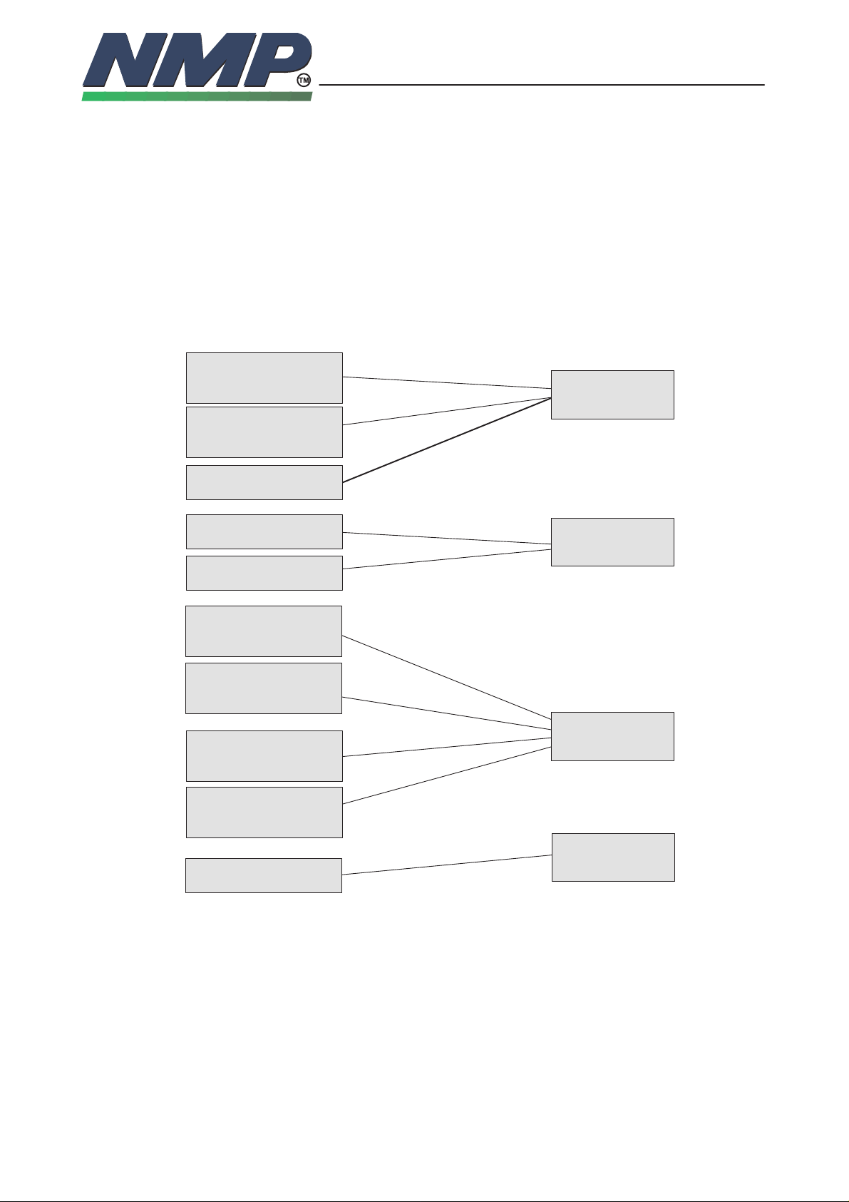
Three modules are described in this document. They are similar in many ways
– the only differences being the keyboard layout. The three modules are used
in the different GSM , PCN and DCS 1900 phones as shown in following pic-
ture:
PHONES
GSM
NHE–1XN; 05001 14
NHE–4NX; 0500312
PCN
NHK–4XN; 05001 15
NHK–4NX; 0500313
DCS1900
NHB–2NB; 0500498
9–2
Copyright Nokia Mobile Phones
UIF MODULE
DU8
0200173
GSM
NHE–4NY; 0500314
PCN
NHK–4NY; 0500315
GSM
NHE–1XA; 05001 17
NHE–4AX; 0500318
PCN
NHK–1XA; 0500205
NHK–4AX; 0500319
GSM
NHE–1XB; 05001 19
NHE–4BX; 0500316
PCN
NHK–1XB; 0500120
NHK–4BX; 0500317
PCN
NHK–4PT; 0500489
GU3E
0200516
DU9
0200174
DU9B
0200940
Page 3
UIF MODULES DU8, DU9, GU3E
NHE–1/4 NHK–1/4 NHB–2
Hierarchy of Design
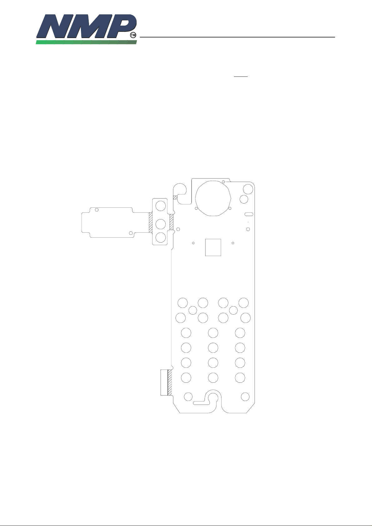
The difference between the three PCB layouts is only the position of the keys &
LEDs (and one less LED on the DU8 version) The DU8 has 20 main keys,
2 volume keys at the side of the flex and a power key in the upper right corner
of the flex. The DU9 has 20 main keys in a slightly different layout and the vol-
ume / power keys combined on one assembly.
The GU3E has one LED less than DU8. Volume and power keys are as in DU8.
Mechanics
06/97JR
Technical Documentation
9–3
Copyright Nokia Mobile Phones
1
30
DU8, DU9 & GU3E Style Flexes
Page 4

UIF MODULES DU8, DU9, GU3E
NHE–1/4 NHK–1/4 NHB–2
06/97JR
Technical Documentation
Technical Specifications
External Signals and Connectors
The UIF module has two connectors, display module connector X1 and UIF
connector X4.
UIF Connector X4
Pin Name Description
1 VL1 Logic supply voltage 4.65V
2, 29 GND Ground
3, 30 VBAT Battery voltage
4 BACKLIGHT Backlights on/off
5 – 11 UIF(0:6) Lines for keyboard read and LCD–controller control
9–4
Copyright Nokia Mobile Phones
12 MIC_ENA Microphone bias enable
13 – 16 COL(0:3) Lines for keyboard write
17 CALL_LED Call led enable
18 MICP Microphone (positive node)
19 MICN Microphone (negative node)
20 EARP Earpiece (negative node)
21 EARN Earpiece (positive node)
22 BUZZER PWM signal buzzer control
23 XPWRON Power key (active low)
24 VA1 Analog supply voltage 4.65V
25 SIMCLK Clock for SIM data
26 SIMRESET Reset for SIM
27 VSIM SIM voltage supply control
28 SIMDATA Serial data for SIM
Page 5

UIF MODULES DU8, DU9, GU3E
NHE–1/4 NHK–1/4 NHB–2
06/97JR
Technical Documentation
Supply voltages and power consumption
Symbol Description Values
VL1 Logic voltage
• typical/nominal
VA Analog voltage
• mic enabled typ/nom current
• max volume level to earphone
typ/nom current
Vbatt Battery voltage
• Buzzer with max volume
typ/nom current
max current
• display illumination
typ/nom current
9–5
Copyright Nokia Mobile Phones
1.5 mA
250 µA
25 mA
85 mA
115 mA
40 mA
• keyboard illumination
typ/nom current
Control Signals
Symbol Description Values
Mic_Enable Microphone enable
Key and LCD light key and LCD backlightning control
Call_Led Call indicator LED control
Warnings and Restrictions
Limited Bending Ability: The flexible circuits are constructed from a lamination
of three layers of polyamide and two layers of copper tracks. The polyamide
has almost unlimited bending capability – but the copper tracks cannot be bent
to tight radii very often. At all times before the flexi circuit is installed into a
phone, bending of the circuit should be avoided if possible. If the flexi circuit
has already been installed into the phone, then care should be taken not to
continuously fold the flexi circuit out flat and then back to its resting position too
often.
• enabled typ/max
• disabledmin/typ/max
• Lights on min/max
• Lights off min/max
• LED on min/max
• LED off min/max
40 mA
0...3 V
VA1–0.4...VA1...VA1+3 V
VA1–1.0...VA1 V
0...2.0 V
VA1–1.0...VA1 V
0...0.4 V
Page 6

UIF MODULES DU8, DU9, GU3E
NHE–1/4 NHK–1/4 NHB–2
Functional Description
The module is connected with 30 pin flex connector to the system board, 24 pin
connector to the LCD module and 6 pin connector to the SIM card.
The module includes following main blocks:
– keyboard
– SIM interface
– illumination
– audio block
– LCD Module interface
Keyboard Scanning
COL(0–4) are used as column lines in keyboard. UIF(0–5) are used as row
lines. They are also multiplexed with display driver control signals.
When a key is pressed the ASIC gets an interrupt from a row and the MCU
starts scanning. One column at a time is written to low and rows are used to
read which key it was. The power off detection is multiplexed with one row;
when all keys on the row seems to be pressed the ASIC knows that power key
is pressed. The power key is also connected to PSL+ to switch the power on.
06/97JR
Technical Documentation
9–6
Copyright Nokia Mobile Phones
Row lines and UIF6 are used for display driver control. UIF(0–3) are used as 4
bit parallel data bus for the driver. UIF4 is used as read/write strobe, UIF5 to
select data or instruction register and UIF6 as enable strobe.
Keyboard and Display illumination
The keyboard illumination is achieved by using two transistors wired as simple
constant current sinks. Each transistor supplies eight leds. The bases of the
transistors are all wired together and supplied by emitter follower V40. The led
current is fixed by the values of R44 and R45 and the ratio of R51 to R52. The
current is about 5 mA/ each LED. Note that on DU9 flexis, the 17
from an additional transistor.
The display illumination operates in a similar way to the keyboard drivers, two
transistors are used to drive eight leds. The current in this case is defined by
the value of R46, R47 and the ratio of R51 to R52. It is about 10 mA/ each LED.
th
led is driven
Page 7

UIF MODULES DU8, DU9, GU3E
NHE–1/4 NHK–1/4 NHB–2
Audio Circuitry
The earpiece is routed directly via series resistors to connector X4. The ear-
piece is dynamic type. The impedance is 32 Ω and sensitivity 118 dB/1 V.
Microphone is of the electret type and needs a voltage supply for operation.
When MIC_ENA is low bias voltage is connected to the microphone via transis-
tor V8. V2 is wired as a switch for VA1, controlled by the microphone enable
line [MICENA]. VA1 is an analogue rail supplied by the PSL+ chip on the sys-
tem board. It is 4.65 V in magnitude. The sensitivity of the microphone is –62
dB (0 dB = 1V/µbar). C26 and C27 in the MIC nodes act as high pass filter with
pulldown resistors on the baseband side.–3 dB point is about 100Hz.
The buzzer is dynamic one and the impedance is 25 ohm. Buzzer is driven
from a two transistor switch which acts as a buffer for a CMOS output signal
applied at BUZZER. The ringing volume is controlled by pulse width modula-
tion.The diode V37 prevents damage to the transistor when switched off, ab-
sorbing the stored energy in the buzzer inductance and suppressing large posi-
tive going spikes on the transistor collectors.
06/97JR
Technical Documentation
9–7
Copyright Nokia Mobile Phones
Small value capacitors are fitted at critical points in the circuit to avoid problems
with rf interference. One is placed directly across the microphone (C15). V9 has
a cap to ground from each of its three terminals (C14, C17 and C21). There is
also capacitors in earphone nodes.
LCD Module Interface
The LCD module includes the LCD and the display driver. The driver TAB is
connected with heat seal connection to the LCD. The LCD is FSTN type. The
duty ratio is1/32 and the bias ratio 1/6.7. Viewing direction is 6 o‘clock.
The display driver is NJU6406–02 from JRC. It has internal clock oscillator and
negative voltage generator. It has 9600 bit character generator ROM and 64 * 8
bits character generator RAM. The display module is connected to the UIF
module with 24 pin soldered connection.
The display module contains an oscillator to generate a negative voltage re-
quired for operation. The oscillator frequency is fixed on the UIF module by the
resistance from pins 2 to 3 of X1, with the values of R6 and R16 shown, the fre-
quency is within 180 kHz to 370 kHz. The negative going pulses appear at pin 9
of X1 where they are smoothed by C1 to give a voltage which is nominally
equal but opposite to VL1.
For correct operation of the display, D.C. voltages between –VL1 and VL1 need
to be generated and fed back to the driver chip, at pins 4 to 8 inclusive (of X1).
The exact voltages depend on the relative values of the resistors R21, R37,
R38, R39, R40 and R33.
Page 8
UIF MODULES DU8, DU9, GU3E
NHE–1/4 NHK–1/4 NHB–2
The display driver is connected to the radio module with a 4 bit data bus. Data
transfer is controlled with the following signals: R/W selects read or write opera-
tion (”0” = write, ”1” = read), Enable activates read/write operations and RS se-
lects the register (”0” : instruction register (writing) or busy flag (reading), ”1” :
data register).
SIM Interface
The SIM interface is the electrical interface between the smart card used in the
GSM and PCN applications and the MCU via the ASIC. Four signals are used
between the SIM card and the ASIC:SIMDATA, SIMCLK, SIMRESET and
VSIM. Serial data is transferred between the card and the ASIC, the clock fre-
quency is 3.25 MHz. When there is no data transfer between the SIM card and
the HP the clock can be reduced to 1.625 MHz. Some cards allow to stop the
clock in that mode. The ASIC also generates the reset for the card and the sup-
ply voltage VSIM.
06/97JR
Technical Documentation
9–8
Copyright Nokia Mobile Phones
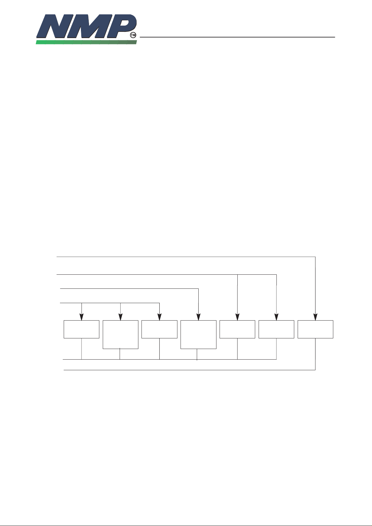
Power Distribution Diagram
VA1
VL1
VSIM
Vbatt
Call
LED
GND
AGND
KEY/
LCD
Lights
Buzzer
SIM card
reader
LCD
Keyboard
scan
Audio
Page 9

UIF MODULES DU8, DU9, GU3E
NHE–1/4 NHK–1/4 NHB–2
06/97JR
Technical Documentation
Circuit Diagram of DU8 (Version 2.7 edit 31)
9–9
Copyright Nokia Mobile Phones
Page 10

UIF MODULES DU8, DU9, GU3E
NHE–1/4 NHK–1/4 NHB–2
06/97JR
Technical Documentation
Circuit Diagram of DU9 (Version 2.7 edit 36)
9–10
Copyright Nokia Mobile Phones
Page 11

UIF MODULES DU8, DU9, GU3E
NHE–1/4 NHK–1/4 NHB–2
06/97JR
Technical Documentation
Circuit Diagram of GU3E (Version 1.0 edit 38)
9–11
Copyright Nokia Mobile Phones
Page 12

UIF MODULES DU8, DU9, GU3E
NHE–1/4 NHK–1/4 NHB–2
06/97JR
Technical Documentation
Layout Diagrams of DU8 (Version 09)
9–12
Copyright Nokia Mobile Phones
Page 13

UIF MODULES DU8, DU9, GU3E
NHE–1/4 NHK–1/4 NHB–2
06/97JR
Technical Documentation
Layout Diagrams of DU9 (Version 11)
9–13
Copyright Nokia Mobile Phones
Page 14

UIF MODULES DU8, DU9, GU3E
NHE–1/4 NHK–1/4 NHB–2
06/97JR
Technical Documentation
Layout Diagrams of GU3E (Version 06)
9–14
Copyright Nokia Mobile Phones
Page 15

UIF MODULES DU8, DU9, GU3E
NHE–1/4 NHK–1/4 NHB–2
06/97JR
Technical Documentation
Copyright Nokia Mobile Phones
Parts List of DU8 EDMS Issue 1.3 Code 0200173
ITEM CODE DESCRIPTION VALUE TYPE
R002 1430151 Chip resistor 10 5 % 0.063 W 0603
R003 1430151 Chip resistor 10 5 % 0.063 W 0603
R004 1430075 Chip resistor 33 k 5 % 0.063 W 0603
R005 1430087 Chip resistor 100 k 5 % 0.063 W 0603
R006 1430057 Chip resistor 8.2 k 5 % 0.063 W 0603
R009 1430087 Chip resistor 100 k 5 % 0.063 W 0603
R010 1430087 Chip resistor 100 k 5 % 0.063 W 0603
R011 1430087 Chip resistor 100 k 5 % 0.063 W 0603
R012 1430087 Chip resistor 100 k 5 % 0.063 W 0603
R013 1430087 Chip resistor 100 k 5 % 0.063 W 0603
R014 1430087 Chip resistor 100 k 5 % 0.063 W 0603
R015 1430087 Chip resistor 100 k 5 % 0.063 W 0603
R016 1430085 Chip resistor 82 k 5 % 0.063 W 0603
R017 1430087 Chip resistor 100 k 5 % 0.063 W 0603
R018 1430087 Chip resistor 100 k 5 % 0.063 W 0603
R021 1430075 Chip resistor 33 k 5 % 0.063 W 0603
R022 1430065 Chip resistor 10 k 5 % 0.063 W 0603
R023 1430065 Chip resistor 10 k 5 % 0.063 W 0603
R024 1430065 Chip resistor 10 k 5 % 0.063 W 0603
R025 1430065 Chip resistor 10 k 5 % 0.063 W 0603
R026 1430065 Chip resistor 10 k 5 % 0.063 W 0603
R028 1430075 Chip resistor 33 k 5 % 0.063 W 0603
R029 1430065 Chip resistor 10 k 5 % 0.063 W 0603
R030 1430051 Chip resistor 4.7 k 5 % 0.063 W 0603
R031 1430051 Chip resistor 4.7 k 5 % 0.063 W 0603
R032 1430013 Chip resistor 330 5 % 0.063 W 0603
R033 1430075 Chip resistor 33 k 5 % 0.063 W 0603
R035 1430035 Chip resistor 1.0 k 5 % 0.063 W 0603
R037 1430063 Chip resistor 12 k 5 % 0.063 W 0603
R038 1430063 Chip resistor 12 k 5 % 0.063 W 0603
R039 1430063 Chip resistor 12 k 5 % 0.063 W 0603
R040 1430063 Chip resistor 12 k 5 % 0.063 W 0603
R044 1430165 Chip resistor 39 5 % 0.063 W 0603
R045 1430165 Chip resistor 39 5 % 0.063 W 0603
R046 1430165 Chip resistor 39 5 % 0.063 W 0603
R047 1430165 Chip resistor 39 5 % 0.063 W 0603
R048 1430035 Chip resistor 1.0 k 5 % 0.063 W 0603
R051 1430045 Chip resistor 2.7 k 5 % 0.063 W 0603
R052 1430043 Chip resistor 2.2 k 5 % 0.063 W 0603
R053 1430013 Chip resistor 330 5 % 0.063 W 0603
R054 1430087 Chip resistor 100 k 5 % 0.063 W 0603
C001 2604248 Tantalum cap. 4.7 u 20 % 16 V 6.0x3.2x2.5
C002 2604431 Tantalum cap. 10 u 20 % 16 V 6.0x3.2x2.5
9–15
Page 16

UIF MODULES DU8, DU9, GU3E
NHE–1/4 NHK–1/4 NHB–2
06/97JR
Technical Documentation
Copyright Nokia Mobile Phones
C003 2310784 Ceramic cap. 100 n 10 % 25 V 0805
C004 2604248 Tantalum cap. 4.7 u 20 % 16 V 6.0x3.2x2.5
C005 2307816 Ceramic cap. 47 n 20 % 25 V 0805
C006 2307816 Ceramic cap. 47 n 20 % 25 V 0805
C007 2307816 Ceramic cap. 47 n 20 % 25 V 0805
C008 2307816 Ceramic cap. 47 n 20 % 25 V 0805
C009 2307816 Ceramic cap. 47 n 20 % 25 V 0805
C010 2307816 Ceramic cap. 47 n 20 % 25 V 0805
C013 2604209 Tantalum cap. 1.0 u 20 % 16 V 3.2x1.6x1.6
C014 2320041 Ceramic cap. 18 p 5 % 50 V 0603
C015 2320041 Ceramic cap. 18 p 5 % 50 V 0603
C021 2320041 Ceramic cap. 18 p 5 % 50 V 0603
C023 2307816 Ceramic cap. 47 n 20 % 25 V 0805
C026 2307816 Ceramic cap. 47 n 20 % 25 V 0805
C027 2307816 Ceramic cap. 47 n 20 % 25 V 0805
C030 2320041 Ceramic cap. 18 p 5 % 50 V 0603
C031 2320041 Ceramic cap. 18 p 5 % 50 V 0603
C040 2320107 Ceramic cap. 10 n 5 % 50 V 0603
B001 5140014 Buzzer transducer 90db 25r pc PCB
B002 5140446 Cond. microphone 62+2dB 2.2k PC PCB
B003 5140576 Dynamic receiver 32r 20x2 20x2
V002 4200829 Transistor BC859C pnp 30 V 0.1 A SOT23
V003 4200811 Transistor BC849C npn 30 V 0.1 A SOT23
V004 4200836 Transistor BCX19 npn 50 V 0.5 A SOT23
V005 4200811 Transistor BC849C npn 30 V 0.1 A SOT23
V008 4200811 Transistor BC849C npn 30 V 0.1 A SOT23
V010 4864384 Led Red 0603
V011 4864388 Led Green 0603
V012 4864388 Led Green 0603
V013 4864388 Led Green 0603
V014 4864388 Led Green 0603
V015 4864388 Led Green 0603
V016 4864388 Led Green 0603
V017 4864388 Led Green 0603
V018 4864388 Led Green 0603
V019 4864388 Led Green 0603
V020 4864388 Led Green 0603
V021 4864388 Led Green 0603
V022 4864388 Led Green 0603
V023 4864388 Led Green 0603
V024 4864388 Led Green 0603
V025 4864388 Led Green 0603
V026 4864388 Led Green 0603
V027 4864388 Led Green 0603
V028 4864388 Led Green 0603
V029 4864388 Led Green 0603
V030 4864388 Led Green 0603
V031 4864388 Led Green 0603
9–16
Page 17

UIF MODULES DU8, DU9, GU3E
NHE–1/4 NHK–1/4 NHB–2
06/97JR
Technical Documentation
Copyright Nokia Mobile Phones
9–17
V032 4864388 Led Green 0603
V033 4864388 Led Green 0603
V034 4864388 Led Green 0603
V036 4111824 Diode BAS16 75 V 250 mA 6 ns SOT23
V037 4111824 Diode BAS16 75 V 250 mA 6 ns SOT23
V040 4200811 Transistor BC849C npn 30 V 0.1 A SOT23
V041 4200836 Transistor BCX19 npn 50 V 0.5 A SOT23
V042 4200836 Transistor BCX19 npn 50 V 0.5 A SOT23
V043 4200836 Transistor BCX19 npn 50 V 0.5 A SOT23
V044 4200836 Transistor BCX19 npn 50 V 0.5 A SOT23
X002 5408804 Sim card reader ccm03–2–1 6polsmd 6POLSMD
4850038 IC, lcd 42dotm 3x7sgm 57ind DSL–12 EU
7310007 Esd tape dmd00741
9460074 Light guide 4c23228 nhj–1DA
9460075 Microphone rubber 4d22908 nhj–1DNHJ–1DA
9480061 Reflector 3c22893 nhj–1DA
9480078 Buzzer gasket 4D23092 NHK–1XA
9480103 Speaker pad2 4D23517 NHK–1XA
9480134 Speaker gasket 4D24016 NHK–1XA
9795021 Main keydome 3C26395 NHC–4NX
9795022 Side keydome 4C26397 NHC–4NX
9855011 FLEXIBLE DU8 140X50X0.3 2D22779
9855011 Flexible du8 140x50x0.3 2D22779
Page 18

UIF MODULES DU8, DU9, GU3E
NHE–1/4 NHK–1/4 NHB–2
06/97JR
Technical Documentation
Copyright Nokia Mobile Phones
Parts List of DU9 EDMS Issue 1.2 Code 0200174
ITEM CODE DESCRIPTION VALUE TYPE
R002 1430151 Chip resistor 10 5 % 0.063 W 0603
R003 1430151 Chip resistor 10 5 % 0.063 W 0603
R004 1430075 Chip resistor 33 k 5 % 0.063 W 0603
R005 1430087 Chip resistor 100 k 5 % 0.063 W 0603
R006 1430057 Chip resistor 8.2 k 5 % 0.063 W 0603
R009 1430087 Chip resistor 100 k 5 % 0.063 W 0603
R010 1430087 Chip resistor 100 k 5 % 0.063 W 0603
R011 1430087 Chip resistor 100 k 5 % 0.063 W 0603
R012 1430087 Chip resistor 100 k 5 % 0.063 W 0603
R013 1430087 Chip resistor 100 k 5 % 0.063 W 0603
R014 1430087 Chip resistor 100 k 5 % 0.063 W 0603
R015 1430087 Chip resistor 100 k 5 % 0.063 W 0603
R016 1430085 Chip resistor 82 k 5 % 0.063 W 0603
R017 1430087 Chip resistor 100 k 5 % 0.063 W 0603
R018 1430087 Chip resistor 100 k 5 % 0.063 W 0603
R021 1430075 Chip resistor 33 k 5 % 0.063 W 0603
R022 1430065 Chip resistor 10 k 5 % 0.063 W 0603
R023 1430065 Chip resistor 10 k 5 % 0.063 W 0603
R024 1430065 Chip resistor 10 k 5 % 0.063 W 0603
R025 1430065 Chip resistor 10 k 5 % 0.063 W 0603
R026 1430065 Chip resistor 10 k 5 % 0.063 W 0603
R028 1430075 Chip resistor 33 k 5 % 0.063 W 0603
R029 1430065 Chip resistor 10 k 5 % 0.063 W 0603
R030 1430051 Chip resistor 4.7 k 5 % 0.063 W 0603
R031 1430051 Chip resistor 4.7 k 5 % 0.063 W 0603
R032 1430013 Chip resistor 330 5 % 0.063 W 0603
R033 1430075 Chip resistor 33 k 5 % 0.063 W 0603
R035 1430035 Chip resistor 1.0 k 5 % 0.063 W 0603
R037 1430063 Chip resistor 12 k 5 % 0.063 W 0603
R038 1430063 Chip resistor 12 k 5 % 0.063 W 0603
R039 1430063 Chip resistor 12 k 5 % 0.063 W 0603
R040 1430063 Chip resistor 12 k 5 % 0.063 W 0603
R044 1430165 Chip resistor 39 5 % 0.063 W 0603
R045 1430165 Chip resistor 39 5 % 0.063 W 0603
R046 1430165 Chip resistor 39 5 % 0.063 W 0603
R047 1430165 Chip resistor 39 5 % 0.063 W 0603
R048 1430035 Chip resistor 1.0 k 5 % 0.063 W 0603
R051 1430045 Chip resistor 2.7 k 5 % 0.063 W 0603
R052 1430043 Chip resistor 2.2 k 5 % 0.063 W 0603
R053 1430013 Chip resistor 330 5 % 0.063 W 0603
R054 1430009 Chip resistor 220 5 % 0.063 W 0603
C001 2604248 Tantalum cap. 4.7 u 20 % 16 V 6.0x3.2x2.5
C002 2604431 Tantalum cap. 10 u 20 % 16 V 6.0x3.2x2.5
9–18
Page 19

UIF MODULES DU8, DU9, GU3E
NHE–1/4 NHK–1/4 NHB–2
06/97JR
Technical Documentation
Copyright Nokia Mobile Phones
C003 2310784 Ceramic cap. 100 n 10 % 25 V 0805
C004 2604248 Tantalum cap. 4.7 u 20 % 16 V 6.0x3.2x2.5
C005 2307816 Ceramic cap. 47 n 20 % 25 V 0805
C006 2307816 Ceramic cap. 47 n 20 % 25 V 0805
C007 2307816 Ceramic cap. 47 n 20 % 25 V 0805
C008 2307816 Ceramic cap. 47 n 20 % 25 V 0805
C009 2307816 Ceramic cap. 47 n 20 % 25 V 0805
C010 2307816 Ceramic cap. 47 n 20 % 25 V 0805
C013 2604209 Tantalum cap. 1.0 u 20 % 16 V 3.2x1.6x1.6
C014 2320041 Ceramic cap. 18 p 5 % 50 V 0603
C015 2320041 Ceramic cap. 18 p 5 % 50 V 0603
C021 2320041 Ceramic cap. 18 p 5 % 50 V 0603
C023 2307816 Ceramic cap. 47 n 20 % 25 V 0805
C026 2307816 Ceramic cap. 47 n 20 % 25 V 0805
C027 2307816 Ceramic cap. 47 n 20 % 25 V 0805
C030 2320041 Ceramic cap. 18 p 5 % 50 V 0603
C031 2320041 Ceramic cap. 18 p 5 % 50 V 0603
C040 2320107 Ceramic cap. 10 n 5 % 50 V 0603
B001 5140014 Buzzer transducer 90db 25r pc PCB
B002 5140446 Cond. microphone 62+–2DB 2.2K PCPCB
B003 5140576 Dynamic receiver 32r 20x2 20x2
V002 4200829 Transistor BC859C pnp 30 V 0.1 A SOT23
V003 4200811 Transistor BC849C npn 30 V 0.1 A SOT23
V004 4200836 Transistor BCX19 npn 50 V 0.5 A SOT23
V005 4200811 Transistor BC849C npn 30 V 0.1 A SOT23
V008 4200811 Transistor BC849C npn 30 V 0.1 A SOT23
V010 4864384 Led Red 0603
V011 4864388 Led Green 0603
V012 4864388 Led Green 0603
V013 4864388 Led Green 0603
V014 4864388 Led Green 0603
V015 4864388 Led Green 0603
V016 4864388 Led Green 0603
V017 4864388 Led Green 0603
V018 4864388 Led Green 0603
V019 4864388 Led Green 0603
V020 4864388 Led Green 0603
V021 4864388 Led Green 0603
V022 4864388 Led Green 0603
V023 4864388 Led Green 0603
V024 4864388 Led Green 0603
V025 4864388 Led Green 0603
V026 4864388 Led Green 0603
V027 4864388 Led Green 0603
V028 4864388 Led Green 0603
V029 4864388 Led Green 0603
V030 4864388 Led Green 0603
V031 4864388 Led Green 0603
9–19
Page 20

UIF MODULES DU8, DU9, GU3E
NHE–1/4 NHK–1/4 NHB–2
06/97JR
Technical Documentation
Copyright Nokia Mobile Phones
9–20
V032 4864388 Led Green 0603
V033 4864388 Led Green 0603
V034 4864388 Led Green 0603
V036 4111824 Diode BAS16 75 V 250 mA 6 ns SOT23
V037 4111824 Diode BAS16 75 V 250 mA 6 ns SOT23
V038 4864388 Led Green 0603
V040 4200811 Transistor BC849C npn 30 V 0.1 A SOT23
V041 4200836 Transistor BCX19 npn 50 V 0.5 A SOT23
V042 4200836 Transistor BCX19 npn 50 V 0.5 A SOT23
V043 4200836 Transistor BCX19 npn 50 V 0.5 A SOT23
V044 4200836 Transistor BCX19 npn 50 V 0.5 A SOT23
X002 5408804 Sim card reader ccm03–2–1 6polsmd 6POLSMD
4850038 IC, lcd 42dotm 3x7sgm 57ind DSL–12 EU
7310007 Esd tape dmd00741
9460074 Light guide 4c23228 nhj–1DA
9460075 Microphone rubber 4d22908 nhj–1DNHJ–1DA
9480061 Reflector 3c22893 nhj–1DA
9480078 Buzzer gasket 4D23092 NHK–1XA
9480103 Speaker pad2 4D23517 NHK–1XA
9480134 Speaker gasket 4D24016 NHK–1XA
9795003 Keydome film 4c22987 nhj–1DA
9855006 FLEXIBLE DU9 140X500.3 3D22779
9855006 Flexible du9 140x500.3 3D22779
Page 21

UIF MODULES DU8, DU9, GU3E
NHE–1/4 NHK–1/4 NHB–2
06/97JR
Technical Documentation
Copyright Nokia Mobile Phones
Parts List of GU3E EDMS Issue 1.3 Code 0200516
ITEM CODE DESCRIPTION VALUE TYPE
R002 1430151 Chip resistor 10 5 % 0.063 W 0603
R003 1430151 Chip resistor 10 5 % 0.063 W 0603
R004 1430075 Chip resistor 33 k 5 % 0.063 W 0603
R005 1430087 Chip resistor 100 k 5 % 0.063 W 0603
R006 1430057 Chip resistor 8.2 k 5 % 0.063 W 0603
R009 1430087 Chip resistor 100 k 5 % 0.063 W 0603
R010 1430087 Chip resistor 100 k 5 % 0.063 W 0603
R011 1430087 Chip resistor 100 k 5 % 0.063 W 0603
R012 1430087 Chip resistor 100 k 5 % 0.063 W 0603
R013 1430087 Chip resistor 100 k 5 % 0.063 W 0603
R014 1430087 Chip resistor 100 k 5 % 0.063 W 0603
R015 1430087 Chip resistor 100 k 5 % 0.063 W 0603
R016 1430085 Chip resistor 82 k 5 % 0.063 W 0603
R017 1430087 Chip resistor 100 k 5 % 0.063 W 0603
R018 1430087 Chip resistor 100 k 5 % 0.063 W 0603
R021 1430075 Chip resistor 33 k 5 % 0.063 W 0603
R022 1430065 Chip resistor 10 k 5 % 0.063 W 0603
R023 1430065 Chip resistor 10 k 5 % 0.063 W 0603
R024 1430065 Chip resistor 10 k 5 % 0.063 W 0603
R025 1430065 Chip resistor 10 k 5 % 0.063 W 0603
R026 1430065 Chip resistor 10 k 5 % 0.063 W 0603
R028 1430075 Chip resistor 33 k 5 % 0.063 W 0603
R029 1430065 Chip resistor 10 k 5 % 0.063 W 0603
R030 1430051 Chip resistor 4.7 k 5 % 0.063 W 0603
R031 1430051 Chip resistor 4.7 k 5 % 0.063 W 0603
R032 1430013 Chip resistor 330 5 % 0.063 W 0603
R033 1430075 Chip resistor 33 k 5 % 0.063 W 0603
R035 1430035 Chip resistor 1.0 k 5 % 0.063 W 0603
R037 1430063 Chip resistor 12 k 5 % 0.063 W 0603
R038 1430063 Chip resistor 12 k 5 % 0.063 W 0603
R039 1430063 Chip resistor 12 k 5 % 0.063 W 0603
R040 1430063 Chip resistor 12 k 5 % 0.063 W 0603
R044 1430165 Chip resistor 39 5 % 0.063 W 0603
R045 1430165 Chip resistor 39 5 % 0.063 W 0603
R046 1430165 Chip resistor 39 5 % 0.063 W 0603
R047 1430165 Chip resistor 39 5 % 0.063 W 0603
R048 1430035 Chip resistor 1.0 k 5 % 0.063 W 0603
R051 1430045 Chip resistor 2.7 k 5 % 0.063 W 0603
R052 1430043 Chip resistor 2.2 k 5 % 0.063 W 0603
R053 1430013 Chip resistor 330 5 % 0.063 W 0603
R054 1430087 Chip resistor 100 k 5 % 0.063 W 0603
R099 1430011 Chip resistor 270 5 % 0.063 W 0603
C001 2604248 Tantalum cap. 4.7 u 20 % 16 V 6.0x3.2x2.5
9–21
Page 22

UIF MODULES DU8, DU9, GU3E
NHE–1/4 NHK–1/4 NHB–2
06/97JR
Technical Documentation
Copyright Nokia Mobile Phones
C002 2604431 Tantalum cap. 10 u 20 % 16 V 6.0x3.2x2.5
C003 2310784 Ceramic cap. 100 n 10 % 25 V 0805
C004 2604248 Tantalum cap. 4.7 u 20 % 16 V 6.0x3.2x2.5
C005 2307816 Ceramic cap. 47 n 20 % 25 V 0805
C006 2307816 Ceramic cap. 47 n 20 % 25 V 0805
C007 2307816 Ceramic cap. 47 n 20 % 25 V 0805
C008 2307816 Ceramic cap. 47 n 20 % 25 V 0805
C009 2307816 Ceramic cap. 47 n 20 % 25 V 0805
C010 2307816 Ceramic cap. 47 n 20 % 25 V 0805
C013 2604209 Tantalum cap. 1.0 u 20 % 16 V 3.2x1.6x1.6
C014 2320041 Ceramic cap. 18 p 5 % 50 V 0603
C015 2320041 Ceramic cap. 18 p 5 % 50 V 0603
C017 2320041 Ceramic cap. 18 p 5 % 50 V 0603
C021 2320041 Ceramic cap. 18 p 5 % 50 V 0603
C023 2307816 Ceramic cap. 47 n 20 % 25 V 0805
C026 2307816 Ceramic cap. 47 n 20 % 25 V 0805
C027 2307816 Ceramic cap. 47 n 20 % 25 V 0805
C030 2320041 Ceramic cap. 18 p 5 % 50 V 0603
C031 2320041 Ceramic cap. 18 p 5 % 50 V 0603
C040 2320107 Ceramic cap. 10 n 5 % 50 V 0603
B001 5140014 Buzzer transducer 90db 25r pc PCB
B002 5140446 Cond. microphone 62+–2dB 2.2K PCPCB
B003 5140576 Dynamic receiver 32r 20x2 20x2
V002 4200829 Transistor BC859C pnp 30 V 0.1 A SOT23
V003 4200811 Transistor BC849C npn 30 V 0.1 A SOT23
V004 4200836 Transistor BCX19 npn 50 V 0.5 A SOT23
V005 4200811 Transistor BC849C npn 30 V 0.1 A SOT23
V008 4200811 Transistor BC849C npn 30 V 0.1 A SOT23
V010 4864394 Led Red 1210
V011 4864388 Led Green 0603
V012 4864388 Led Green 0603
V013 4864388 Led Green 0603
V014 4864388 Led Green 0603
V015 4864388 Led Green 0603
V016 4864388 Led Green 0603
V017 4864388 Led Green 0603
V018 4864388 Led Green 0603
V019 4864388 Led Green 0603
V020 4864388 Led Green 0603
V021 4864388 Led Green 0603
V022 4864388 Led Green 0603
V024 4864388 Led Green 0603
V026 4864388 Led Green 0603
V027 4864388 Led Green 0603
V028 4864388 Led Green 0603
V029 4864388 Led Green 0603
V030 4864388 Led Green 0603
V031 4864388 Led Green 0603
9–22
Page 23

UIF MODULES DU8, DU9, GU3E
NHE–1/4 NHK–1/4 NHB–2
06/97JR
Technical Documentation
Copyright Nokia Mobile Phones
9–23
V032 4864388 Led Green 0603
V033 4864388 Led Green 0603
V034 4864388 Led Green 0603
V036 4111824 Diode BAS16 75 V 250 mA 6 ns SOT23
V037 4111824 Diode BAS16 75 V 250 mA 6 ns SOT23
V038 4864388 Led Green 0603
V040 4200811 Transistor BC849C npn 30 V 0.1 A SOT23
V041 4200836 Transistor BCX19 npn 50 V 0.5 A SOT23
V042 4200836 Transistor BCX19 npn 50 V 0.5 A SOT23
V043 4200836 Transistor BCX19 npn 50 V 0.5 A SOT23
V044 4200836 Transistor BCX19 npn 50 V 0.5 A SOT23
X002 5408804 Sim card reader ccm03–2–1 6polsmd 6POLSMD
4850038 IC, lcd 42dotm 3x7sgm 57ind DSL–12 EU
7310007 Esd tape dmd00741
9460074 Light guide 4c23228 nhj–1DA
9460075 Microphone rubber 4d22908 nhj–1DNHJ–1DA
9480061 Reflector 3c22893 nhj–1DA
9480078 Buzzer gasket 4D23092 NHK–1XA
9480103 Speaker pad2 4D23517 NHK–1XA
9480134 Speaker gasket 4D24016 NHK–1XA
9795004 Keydome pwr 4C23200 NHE–1XN
9795006 Keydome side 4C23199 NHE–1XN
9855019 PCB GU3E 141X104X02 D 2/PA
9855019 PC board GU3E 141x104x02 d 2/pa
Page 24

UIF MODULES DU8, DU9, GU3E
NHE–1/4 NHK–1/4 NHB–2
06/97JR
Technical Documentation
9–24
Copyright Nokia Mobile Phones
This page intentionally left blank.
 Loading...