NEC UPA800TF, UPA800T-T1B, UPA800T Datasheet

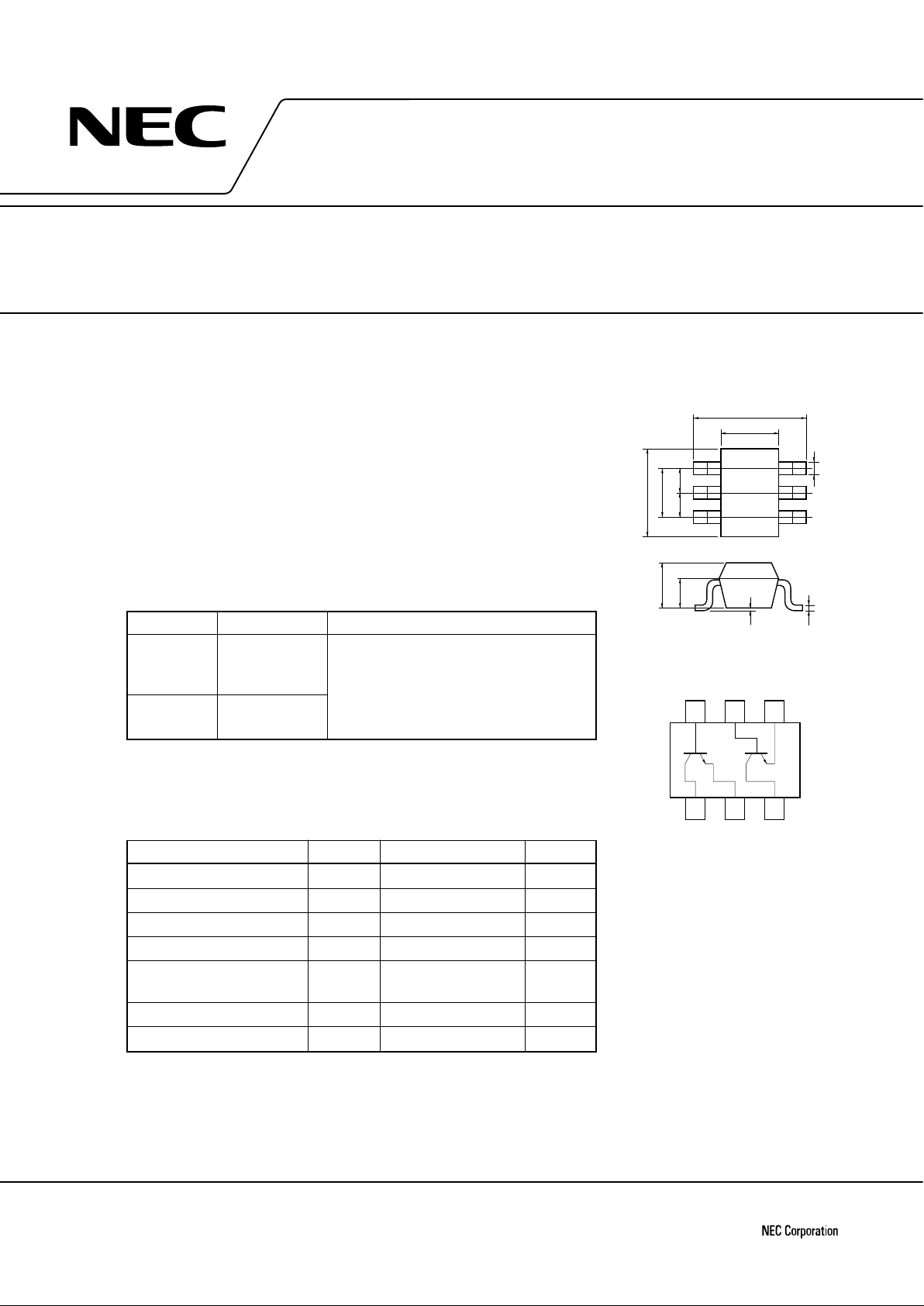
PACKAGE DRAWINGS
(Unit: mm)
SILICON TRANSISTOR
The µPA800T has built-in 2 low-voltage transistors which are designed
to amplify low noise in the VHF band to the UHF band.
FEATURES
• Low Noise
NF = 1.9 dB TYP. @ f = 2 GHz, VCE = 1 V, IC = 3 mA
• High Gain
|S
21e|
2
= 6.5 dB TYP. @ f = 2 GHz, VCE = 1 V, IC = 3 mA
• A Mini Mold Package Adopted
• Built-in 2 Transistors (2 × 2SC4228)
ORDERING INFORMATION
PART NUMBER
QUANTITY PACKING STYLE
µ
PA800T Loose products Embossed tape 8 mm wide. Pin 6 (Q1
(50 PCS) Base), Pin 5 (Q2 Base), Pin 4 (Q2 Emitter)
face to perforation side of the tape.
µ
PA800T-T1 Taping products
(3 KPCS/Reel)
Remark If you require an evaluation sample, please contact an NEC
Sales Representative. (Unit sample quantity is 50 pcs.)
ABSOLUTE MAXIMUM RATINGS (TA = 25 °C)
PARAMETER SYMBOL RATING UNIT
Collector to Base Voltage VCBO 20 V
Collector to Emitter Voltage VCEO 10 V
Emitter to Base Voltage VEBO 1.5 V
Collector Current IC 35 mA
Total Power Dissipation PT 150 in 1 element mW
200 in 2 elements
Note
Junction Temperature Tj 150 ˚C
Storage Temperature Tstg –65 to +150 ˚C
Note 110 mW must not be exceeded in 1 element.
µ
PA800T
HIGH-FREQUENCY LOW NOISE AMPLIFIER
NPN SILICON EPITAXIAL TRANSISTOR
(WITH BUILT-IN 2 ELEMENTS) MINI MOLD
PIN CONFIGURATION (Top View)
©
1995
PRELIMINARY DATA SHEET
Printed in Japan
Document No. ID-3634
(O.D. No. ID-9141)
Date Published April 1995 P
The information in this document is subject to change without notice.
2.1±0.1
1.25±0.1
123
654
0.2
–0
+0.1
0.650.65
1.3
2.0±0.2
0.9±0.1
0.7
0~0.1
0.15
–0
+0.1
654
Q
1
Q
2
123
PIN CONNECTIONS
1. Collector (Q1)
2. Emitter (Q1)
3. Collector (Q2)
4. Emitter (Q2)
5. Base (Q2)
6. Base (Q1)
XY

µ
PA800T
2
ELECTRICAL CHARACTERISTICS (TA = 25 °C)
PARAMETER SYMBOL CONDITION MIN. TYP. MAX. UNIT
Collector Cutoff Current ICBO VCB = 10 V, IE = 0 1.0
µ
A
Emitter Cutoff Current IEBO VEB = 1 V, IC = 0 1.0
µ
A
DC Current Gain hFE VCE = 3 V, IC = 5 mA
Note 1
80 200
Gain Bandwidth Product fT VCE = 3 V, IC = 5 mA 5.5 80 GHz
Feed-back Capacitance Cre VCB = 3 V, IE = 0, f = 1 MHz
Note 2
0.7 pF
Insertion Power Gain (1) |S21e|2VCE = 1 V, IC = 3 mA, f = 2 GHz 4.5 6.5 dB
Insertion Power Gain (2) |S21e|2VCE = 3 V, IC = 5 mA, f = 2 GHz 5.5 7.5 dB
Noise Figure (1) NF VCE = 1 V, IC = 3 mA, f = 2 GHz 1.9 3.2 dB
Noise Figure (2) NF VCE = 3 V, IC = 5 mA, f = 2 GHz 1.9 3.2 dB
Notes 1. Pulse Measurement: Pw ≤ 350 µs, Duty cycle ≤ 2 %
2. Measured with 3-pin bridge, emitter and case should be connected to guard pin of bridge.
hFE CLASSIFICATION
Rank KB
Marking RL
hFE Value 80 to 200
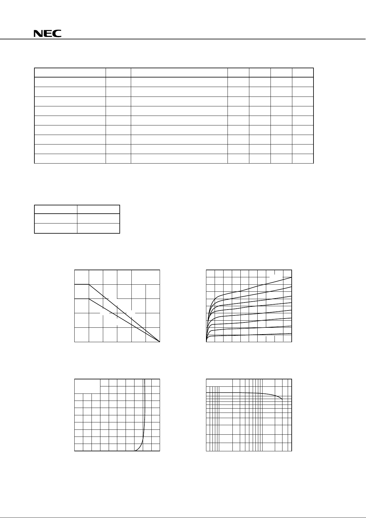
TYPICAL CHARACTERISTICS (TA = 25 °C)
100
0
5
0
10
0.5
50 100 150
200
5 1.0
10
15
20
0 0.5 1.0
10
20
1 5 10 50
20
50
100
200
V
CE = 3 V
VCE = 3 V
120 A
100 A
80 A
IB = 20 A
Total Power Dissipation PT (mW)
Ambient Temperature TA (°C) Collector to Emitter Voltage VCE (V)
Collector Current IC (mA)
Collector Current I
C (mA)
Base to Emitter Voltage VBE (V)
Collector Current I
C (mA)
DC Current Gain hFE
60 A
40 A
25
Free Air
IC - VBE Characteristics hFE - IC Characteristics
PT - TA Characteristics
I
C - VCE Characteristics
2 Elements in Total
Per Element
160 A
µ
140 A
µ
µ
µ
µ
µ
µ
µ
 Loading...