


MXIC MX26L6420XBI-12, MX26L6420MC-90, MX26L6420TI-12, MX26L6420XAI-12, MX26L6420XAC-90 Datasheet
...
FEATURES
ADVANCED INFORMATION
MX26L6420
64M-BIT [4M x 16] CMOS
MULTIPLE-TIME-PROGRAMMABLE EPROM
• 4,194,304 x 16 byte structure
• Single Power Supply Operation
- 2.7 to 3.6 volt for read, erase, and program
operations
• Low Vcc write inhibit is equal to or less than 2.5V
• Compatible with JEDEC standard
• High Performance
- Fast access time: 90/120ns (typ.)
- Fast program time: 140s/chip (typ.)
- Fast erase time: 150s/chip (typ.)
• Low Power Consumption
- Low active read current: 17mA (typ.) at 5MHz
- Low standby current: 30uA (typ.)
• Minimum 100 erase/program cycle
GENERAL DESCRIPTION
The MX26L6420 is a 64M bit MTP EPROMTM organized
as 4M bytes of 16 bits. MXIC's MTP EPROM
most cost-effective and reliable read/write non-volatile
random access memory. The MX26L6420 is packaged in
44SOP, 48-pin TSOP, 48-ball CSP and 63-ball CSP. It is
designed to be reprogrammed and erased in system or in
standard EPROM programmers.
TM
offer the
• Status Reply
- Data polling & Toggle bits provide detection of
program and erase operation completion
• 12V ACC input pin provides accelerated program
capability
• Output voltages and input voltages on the device is
deterined by the voltage on the VI/O pin.
- VI/O voltage range:1.65V~3.6V
• 10 years data retention
• Package
- 44-Pin SOP
- 48-Pin TSOP
- 48-Ball CSP
- 63-Ball CSP
MXIC's MTP EPROM
memory contents even after 100 erase and program
cycles. The MXIC cell is designed to optimize the erase
and program mechanisms. In addition, the combination of
advanced tunnel oxide processing and low internal
electric fields for erase and programming operations
produces reliable cycling.
TM
technology reliably stores
The standard MX26L6420 offers access time as fast as
90ns, allowing operation of high-speed microprocessors
without wait states. To eliminate bus contention, the
MX26L6420 has separate chip enable (CE) and output
enable OE controls. MXIC's MTP EPROMTM augment
EPROM functionality with in-circuit electrical erasure and
programming. The MX26L6420 uses a command register
to manage this functionality.
P/N:PM0823 REV. 0.5, JAN. 29, 2002
The MX26L6420 uses a 2.7V to 3.6V VCC supply to
perform the High Reliability Erase and auto Program/
Erase algorithms.
The highest degree of latch-up protection is achieved with
MXIC's proprietary non-epiprocess. Latch-up protection
is proved for stresses up to 100 milliamps on address and
data pin from -1V to VCC +1V.
1
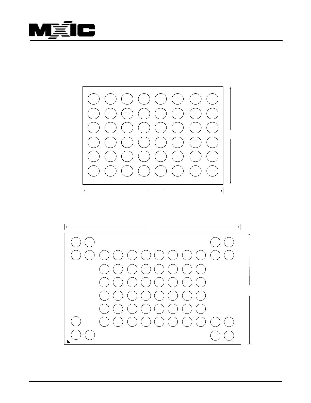
PIN CONFIGURATION
48 CSP Ball pitch=0.75mm for MX26L6420XA (TOP view, Ball down)
12345678
MX26L6420
A
B
C
D
E
F
A13
A14
A15
A16
V I/O
GND
A11
A10
A12
Q14
Q15
Q7
A8
WE
A9
Q5
Q6
Q13
ACC NC
RESET
A21
Q11
Q12
Q4
A18
A20
Q2
Q3
VCC
A19
A17
A6
Q8
Q9
Q10
A7
A5
A3
CE
Q0
Q1
13.0 mm
63 CSP Ball pitch=0.8mm for MX26L6420XB(TOP view, Ball down)
13.0 mm
8
NC
NC
A4
A2
A1
A0
GND
OE
NC*
8.0 mm
NC*
P/N:PM0823
7
6
5
4
3
2
1
* Ball are shorted together via the substrate but not connected to the die.
NC
NC
NC*
NC*
NC*
BCDEFGHJK LM
A
A13
A9
WE
NC
A7
A3
A12
A8
RESET
ACC
A17
A4
A14
A10
A21
A18
A6
A2
A15
A11
A19
A20
A5
A1
A16
VIO
Q7
Q14
Q12
Q5
Q2
Q10
Q0
Q8
A0
CE
Q15
Q13
VCC
Q11
Q9
OE
GND
Q6
Q4
Q3
Q1
GND
NC*
NC*
NC*
NC*
8.0 mm
NC*
NC*
REV. 0.5, JAN. 29, 2002
2
MX26L6420
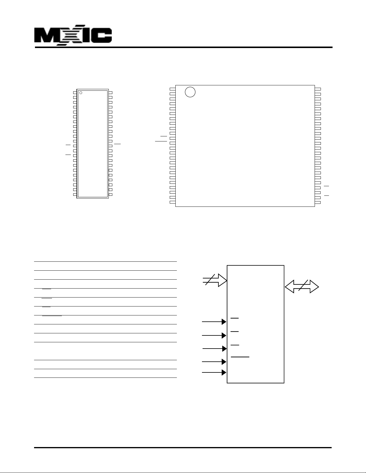
44 SOP
A21
A18
A17
CE
GND
OE
Q0
Q8
Q1
Q9
Q2
Q10
Q3
Q11
48 TSOP
44
A20
43
2
3
4
A7
5
A6
6
A5
7
A4
8
A3
9
A2
10
A1
11
A0
12
13
14
MX26L6420
15
16
17
18
19
20
21
22
A19
42
A8
41
A9
40
A10
39
A11
38
A12
37
A13
36
A14
35
A15
34
A16
33
WE
32
GND
31
Q15
30
Q7
29
Q14
28
Q6
27
Q13
26
Q5
25
Q12
24
Q4
23
VCC
A15
A14
A13
A12
A11
A10
A21
A20
WE
RESET
ACC
VCC
A19
A18
A17
1
2
3
4
5
6
7
A9
8
A8
9
10
11
12
13
14
15
16
17
18
A7
19
A6
20
A5
21
A4
22
A3
23
A2
24
A1
MX26L6420
A16
48
V
47
46
45
44
43
42
41
40
39
38
37
36
35
34
33
32
31
30
29
28
27
26
25
I/O
GND
Q15
Q7
Q14
Q6
Q13
Q5
Q12
Q4
V
CC
Q11
Q3
Q10
Q2
Q9
Q1
Q8
Q0
OE
GND
CE
A0
PIN DESCRIPTION
SYMBOL PIN NAME
A0~A21 Address Input
Q0~Q15 Data Inputs/Outputs
CE Chip Enable Input
WE Write Enable Input
OE Output Enable Input
RESET Hardware Reset Pin, Active Low
VC C +3.0V single power supply
ACC Hardware Acceleration Pin
V I/O I/O power supply (For 48 TSOP and
63-CSP package only)
GN D Device Ground
N C Pin Not Connected Internally
LOGIC SYMBOL
21
A0-A21
CE
OE
WE
RESET
ACC
16
Q0-Q15
P/N:PM0823
REV. 0.5, JAN. 29, 2002
3
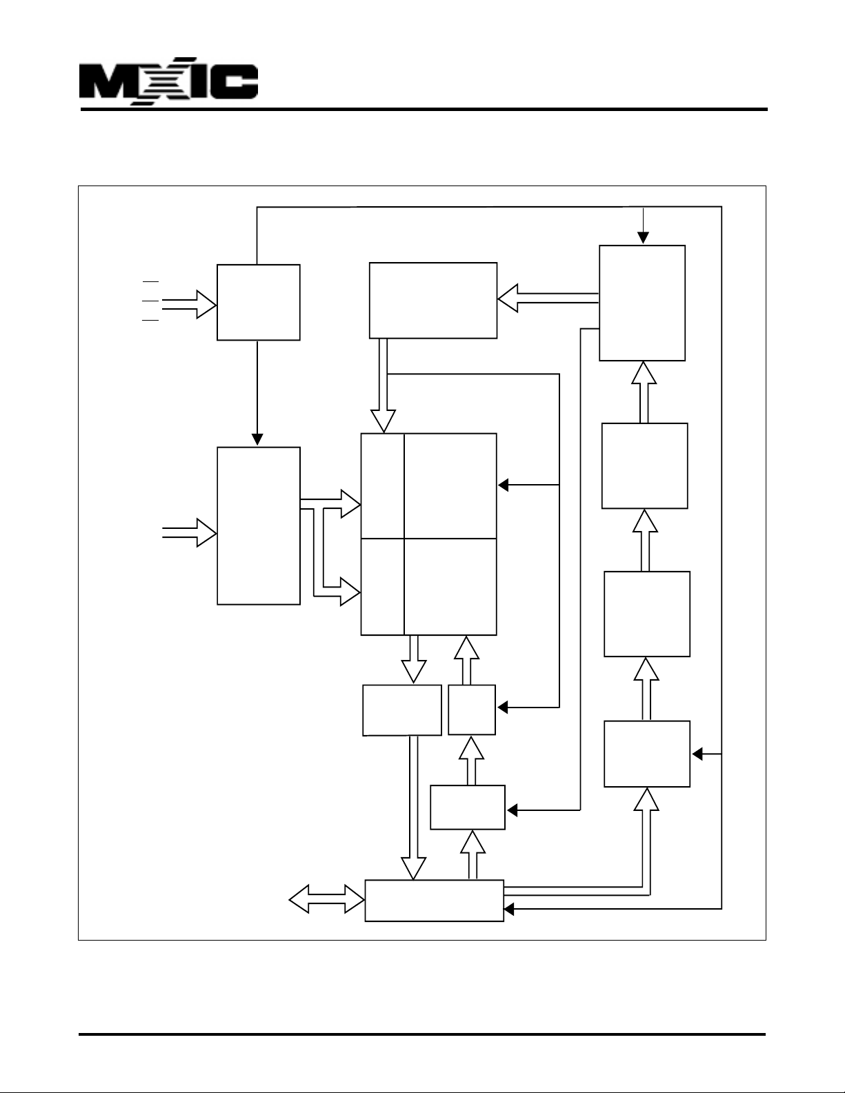
BLOCK DIAGRAM
CE
OE
WE
CONTROL
INPUT
LOGIC
PROGRAM/ERASE
HIGH VOLT A GE
MX26L6420
WRITE
STATE
MACHINE
(WSM)
A0-A21
ADDRESS
LATCH
AND
BUFFER
X-DECODER
MX26L6420
FLASH
ARRA Y
Y-DECODER
Y-PASS GATE
SENSE
AMPLIFIER
DATA LATCH
STATE
REGISTER
ARRAY
SOURCE
HV
COMMAND
DATA
DECODER
PGM
DATA
HV
COMMAND
DATA LATCH
PROGRAM
P/N:PM0823
Q0-Q15
I/O BUFFER
REV. 0.5, JAN. 29, 2002
4

MX26L6420
AUTOMATIC PROGRAMMING
The MX26L6420 is word programmable using the Automatic Programming algorithm. The Automatic Progr amming algorithm makes the external system do not need
to have time out sequence nor to verify the data programmed. The typical chip programming time at room
temperature of the MX26L6420 is less than 150 seconds.
AUTOMATIC PROGRAMMING ALGORITHM
MXIC's Automatic Programming algorithm require the user
to only write program set-up commands (including 2 unlock write cycle and A0H) and a program command (program data and address). The de vice automatically times
the programming pulse width, provides the program verification, and counts the number of sequences. A status
bit similar to DATA polling and a status bit toggling between consecutive read cycles, provide feedback to the
user as to the status of the programming operation.
AUTOMATIC CHIP ERASE
ming and erase operations. All address are latched on
the falling edge of WE or CE, whiche ver happens later.
All data are latched on rising edge of WE or CE, whichever happens first.
MXIC's Flash technology combines years of EPROM
experience to produce the highest levels of quality, reliability, and cost effectiveness. The MX26L6420 electrically erases all bits simultaneously using Fowler-Nordheim tunneling. The bytes are programmed b y using the
EPROM programming mechanism of hot electron injection.
During a program cycle, the state-machine will control
the program sequences and command register will not
respond to any command set. After the state machine
has completed its task, it will allow the command register to respond to its full command set.
The entire chip is bulk erased using 50 ms erase pulses
according to MXIC's Automatic Chip Erase algorithm.
T ypical erasure at room temper ature is accomplished in
less than 90 seconds. The Automatic Erase algorithm
automatically programs the entire array prior to electrical
erase. The timing and verification of electrical erase are
controlled internally within the device.
AUTOMATIC ERASE ALGORITHM
MXIC's Automatic Erase algorithm requires the user to
write commands to the command register using standard microprocessor write timings. The device will automatically pre-program and verify the entire arra y. Then
the device automatically times the erase pulse width,
provides the erase verification, and counts the number
of sequences. A status bit toggling between consecutive read cycles provides feedback to the user as to the
status of the programming operation.
Register contents serve as inputs to an internal statemachine which controls the erase and programming circuitry . During write cycles, the command register internally latches address and data needed for the program-
P/N:PM0823
REV. 0.5, JAN. 29, 2002
5
MX26L6420
Table 1
BUS OPERATION(1)
Operation CE OE WE RESET Address Q15~Q0
Read L L H H A
Write(Note 1) L H L H A
IN
IN
D
OUT
D
IN
Standby VCC±0.3V X X VCC±0.3V X High-Z
Output Disable L H H H X High-Z
Reset X X X L X High-Z
Legend:
L=Logic LOW=VIL,H=Logic High=VIH,VID=12.0±0.5V,X=Don't Care, AIN=Address IN, DIN=Data IN, D
=Data OUT
OUT
Notes:
1. When the ACC pin is at VHH, the device enters the accelerated program mode. See "Accelerated Prog ram Operations"
for more information.
Table 2. AUTOSELECT CODES (High Voltage Method)
A5 A8 A14
Operation CE OE WE A0 A1 to A6 to A9 to A15~A21 Q15~Q0
A2 A7 A10
Read Silicon ID L L H L L X L X V
X X00 C2 H
ID
Manufactures Code
Read Silicon ID L L H H L X L X V
X X 22FCH
ID
Device Code
Secured Silscon xx88h
Sector Indicator L L H H H X L X V
X X (factory locked)
ID
Bit (Q7) xx08h
(non-factory locked)
P/N:PM0823
REV. 0.5, JAN. 29, 2002
6

MX26L6420
REQUIREMENTS FOR READING ARRAY
DATA
To read array data from the outputs, the system must
drive the CE and OE pins to VIL. CE is the po wer control
and selects the device. OE is the output control and gates
array data to the output pins. WE should remain at VIH.
The internal state machine is set for reading array data
upon device power-up, or after a hardware reset. This
ensures that no spurious alteration of the memory contect
occurs during the power transition. No command is
necessary in this mode to obtain array data. Standard
microprocessor read cycles that assert valid address on
the device address inputs produce valid data on the device
data outputs. The de vice remains enabled for read access
until the command register contents are altered.
WRITE COMMANDS/COMMAND
SEQUENCES
To program data to the device or erase memory , the
system must drive WE and CE to VIL, and OE to VIH.
An erase operation can erase the entire device. The
"Writing specific address and data commands or
sequences into the command register initiates device
operations. Table 1 defines the valid register command
sequences. Writing incorrect address and data values or
writing them in the improper sequence resets the device
to reading array data."section has details on erasing the
entire chip.
After the system writes the autoselect command
sequence, the device enters the autoselect mode. The
system can then read autoselect codes from the internal
reqister (which is separate from the memory array) on
Q15-Q0. Standard read cycle timings apply in this mode.
Refer to the Autoselect Mode and Autoselect Command
Sequence section for more information.
ICC2 in the DC Characteristics table represents the active
current specification for the write mode. The "AC
Characteristics" section contains timing specification
table and timing diagrams for write operations.
STANDBY MODE
MX26L6420 can be set into Standby mode with two different approaches. One is using both CE and RESET
pins and the other one is using RESET pin only .
When using both pins of CE and RESET, a CMOS
Standby mode is achieved with both pins held at Vcc ±
0.3V . Under this condition, the current consumed is less
than 50uA (typ.). If both of the CE and RESET are held
at VIH, b ut not within the range of VCC ± 0.3V , the de vice
will still be in the standby mode, but the standby currect
will be larger. During Auto Algorithm operation, Vcc active current (Icc2) is required even CE = "H" until the
operation is complated. The de vice can be read with standard access time (tCE) from either of these standby
modes.
When using only RESET, a CMOS standby mode is
achieved with RESET input held at Vss ± 0.3V, Under
this condition the current is consumed less than 50uA
(typ.). Once the RESET pin is taken high,the device is
back to active without recovery delay.
In the standby mode the outputs are in the high impedance state, independent of the OE input.
MX26L6420 is capable to provide the Automatic Standby
Mode to restrain power consumption during read-out of
data. This mode can be used eff ectively with an application requested low power consumption such as handy
terminals.
To active this mode, MX26L6420 automatically switch
themselves to low power mode when MX26L6420 addresses remain stable during access time of tACC+30ns.
It is not necessary to control CE, WE, and OE on the
mode. Under the mode, the current consumed is typically 50uA (CMOS level).
OUTPUT DISABLE
With the OE input at a logic high level (VIH), output from
the devices are disabled. This will cause the output pins
to be in a high impedance state.
P/N:PM0823
REV. 0.5, JAN. 29, 2002
7
MX26L6420
RESET OPERATION
The RESET pin provides a hardware method of resetting
the device to reading arra y data. When the RESET pin is
driven low for at least a period of tRP, the device
immediately terminates any operation in progress,
tristates all output pins, and ignores all read/write
commands for the duration of the RESET pluse. The
device also resets the internal state machine to reading
array data. The operation that was interrupted should be
reinitated once the device is ready to accept another
command sequence, to ensure data integrity
Current is reduced for the duration of the RESET pulse.
When RESET is held at VSS±0.3V, the device draws
CMOS standby current (ICC4). If RESET is held at VIL
but not within VSS±0.3V, the standby current will be
greater.
The RESET pin may be tied to system reset circuitry . A
system reset would that also reset the MTP EPROM.
Refer to the AC Characteristics tables for RESET
parameters and to Figure 14 for the timing diagram.
SILICON ID READ OPERATION
Table 3
VCC / VI/O V oltage Range
Part No. VCC=2.7V to 3.6VVCC=2.7V to 3.6V
VI/O=2.7V to 3.6VVI/O=1.65V to 2.6V
MX26L6420-90 90ns 100ns
MX26L6420-12 120ns 130ns
Notes: T ypical v alues measured at VCC=2.7V to 3.6V,
VI/O=2.7V to 3.6V
DATA PROTECTION
The MX26L6420 is designed to offer protection against
accidental erasure or programming caused by spurious
system level signals that may exist during power transition. During power up the device automatically resets
the state machine in the Read mode. In addition, with
its control register architecture, alteration of the memory
contents only occurs after successful completion of specific command sequences. The device also incorporates
several features to prevent inadvertent write cycles resulting from VCC pow er-up and power-down transition or
system noise.
MTP EPROM are intended for use in applications where
the local CPU alters memory contents. As such, manufacturer and device codes must be accessible while the
device resides in the target system. EPROM programmers typically access signature codes by raising A9 to
a high voltage. How ever , multiple xing high voltage onto
address lines is not generally desired system design practice.
MX26L6420 provides hardware method to access the
silicon ID read operation. Which method requires VID on
A9 pin, VIL on CE, OE, A6, and A1 pins. Which apply
VIL on A0 pin, the device will output MXIC's manufacture code of C2H. Which apply VIH on A0 pin, the device
will output MX26L6420 device code of 22FCH.
VI/O PIN OPERATION
MX26L6420 is capable to provide the I/O prower supply
(VI/O) pin to control Input/Output voltage levels of the
device. The data outputs and voltage tolerated at its data
input is determined by the voltage on the VI/O pin. This
device is allows to operate in 1.8V or 3V system as required.
SECURED SILICON SECTOR
The MX26L6420 features a Flash memory region where
the system may access through a command sequence
to create a permant part identification as so called Electronic Serial Number (ESN) in the device. Once this region is programmed, any further modification on the region is impossible. The secured silicon sector is a 512
words in length, and uses a Secured Silicon Sector Indicator Bit (Q7) to indicate whether or not the Secured
Silicon Sector is locked when shipped from the f actory.
This bit is permanently set at the factory and cannot be
changed, which prevent duplication of a factory locked
part. This ensures the security of the ESN once the product is shipped to the field.
The MX26L6420 offers the device with Secured Silicon
Sector either factory locked or custor lockab le. The factory-locked version is always protected when shipped
from the factory , and has the Secured Silicon Sector
Indicator Bit permanently set to a "1". The customerlockable version is shipped with the Secured Silicon
Sector unprotected, allowing customer to utilize that sector in any form they pref er . The customer-loc kable v er-
P/N:PM0823
REV. 0.5, JAN. 29, 2002
8

MX26L6420
sion has the secured sector Indicator Bit permanently
set to a "0". Therefore, the Secured Silicon Sector Indicator Bit permanently set to a "0". Therefore, the Second
Silicon Sector Indicator Bit prevents customer, lockable
device from being used to replace devices that are factory locked.
The system access the Secured Silicon Sector through
a command sequence (refer to "Enter Secured Silicon/
Exit Secured Silicon Sector command Sequence). After
the system has written the Enter Secured Silicon Sector
command sequence, it may read the Secured Silicon
Sector by using the address normally occupied by the
address 000000h-0001FFh. This mode of operation continues until the system issues the Exit Secured Silicon
Sector command sequence, or until power is removed
from the device. On power-up, or following a hardware
reset, the device rever ts to sending command to address 000000h-0001FFFh.
LOW VCC WRITE INHIBIT
When VCC is less than VLKO the device does not accept any write cycles. This protects dataduring VCC
power-up and power-do wn. The command register and
all internal program/erase circuits are disabled, and the
device resets. Subsequent writes are ignored until VCC
is greater thanVLK O. The system must provide the proper
signals to the control pins to prevent unintentional write
when VCC is greater than VLK O.
FACTORY LOCKED:Secured Silicon Sector
Programmed and Protected At the Factory
In device with an ESN, the Secured Silicon Sector is
protected when the device is shipped from the factory.
The Secured Silicon Sector cannot be modified in any
way . A f actory locked device has an 8-word random ESN
at address 000000h-000007h.
CUSTOMER LOCKABLE:Secured Silicon
Sector NOT Programmed or Protected At the
Factory
As an alternative to the factory-locked version, the device
may be ordered such that the customer may program
and protect the 512-word Secured Silicon Sector.
Programming and protecting the Secured Silicon Sector
must be used with caution since, once protected, there
is no procedure available for unprotecting the Secured
Silicon Sector area and none of the bits in the Secured
Silicon Sector memory space can be modified in any
way.
The Secured Silicon Sector area can be protected using
the following procedures:
Write the three-cycle Enter Secured Silicon Sector Region
command sequence. This allows in-system protection
of the Secured Silicon Sector without raising any device
pin to a high voltage. Note that method is only applicable
to the Secured Silicon Sector.
WRITE PULSE "GLITCH" PROTECTION
Noise pulses of less than 5ns(typical) on CE or WE will
not initiate a write cycle.
LOGICAL INHIBIT
Writing is inhibited by holding any one of OE = VIL, CE =
VIH or WE = VIH. To initiate a wr ite cycle CE and WE
must be a logical zero while OE is a logical one.
POWER-UP SEQUENCE
The MX26L6420 powers up in the Read only mode. In
addition, the memory contents may only be altered after
successful completion of the predefined command sequences.
P/N:PM0823
Once the Secured Silicon Sector is programmed, locked
and verified, the system must write the Exit Secured
Silicon Sector Region command sequence to return to
reading and writing the remainder of the array .
REV. 0.5, JAN. 29, 2002
9
SOFTWARE COMMAND DEFINTIONS
MX26L6420
Device operations are selected by writing specific ad-
will reset the device(when applicable).
dress and data sequences into the command register.
Writing incorrect address and data values or writing them
in the improper sequence will reset the device to the
read mode. Table 4 defines the valid register command
All addresses are latched on the falling edge of WE or
CE, whichever happens later . All data are latched on rising edge of WE or CE, whiche ver happens first.
sequences. Either of the two reset command sequences
TABLE4. MX26L6420 COMMAND DEFINITIONS
First Bus Second Bus Third Bus Fourth Bus Fifth Bus Sixth Bus
Command Bus Cycle Cycle Cycle Cycle Cycle Cycle
Cycle Addr Data Addr Data Addr Data Addr Data Addr Data Addr Data
Read(Note 5) 1 RA RD
Reset(Note 6) 1 XXX F0
Autoselect(Note 7)
Manufacturer ID 4 555 AA 2AA 55 555 90 X00 C2
Device ID 4 555 AA 2AA 55 555 90 X01 22FC
Secured Sector 4 55 5 AA 2AA 55 555 90 x0 3 see
Factory Protect Note9
Enter Secured Silicon 3 55 5 AA 2AA 55 5 55 88
Sector
Exit Secured Silicon 4 55 5 AA 2AA 55 5 55 9 0 xxx 00
Sector
Porgram 4 555 AA 2AA 55 5 55 A0 PA PD
Chip Erase 6 55 5 AA 2 AA 5 5 55 5 8 0 55 5 AA 2AA 55 5 55 10
Legend:
X=Don't care
RA=Address of the memory location to be read.
PD=Data to be programmed at location PA. Data is
latched on the rising edge of WE or CE pulse.
RD=Data read from location RA during read operation.
P A=Address of the memory location to be programmed.
Addresses are latched on the falling edge of the WE or
CE pulse.
Notes:
1.See Table 1 for descriptions of bus operations.
2.All values are in hexadecimal.
3.Except when reading array or autoselect data, all bus cycles are write operation.
4.Address bits are don't care for unlock and command cycles, e xcept when PA is required.
5.No unlock or command cycles required when device is in read mode.
6.The Reset command is required to return to the read mode when the device is in the autoselect mode or if Q5 goes
high.
7.The fourth cycle of the autoselect command sequence is a read cycle.
8.In the third and fourth cycles of the command sequence, set A21=0.
8.Command is valid when device is ready to read array data or when device is in autoselect mode.
9.The data is 88h for factory locked and 08h for non-factory locked.
P/N:PM0823
10
REV. 0.5, JAN. 29, 2002

MX26L6420
READING ARRAY DATA
The device is automatically set to reading array data
after device power-up. No commands are required to
retrieve data. The device is also ready to read arra y data
after completing an Automatic Program or Automatic
Erase algorithm.
The system must issue the reset command to re-enable the device for reading array data if Q5 goes high, or
while in the autoselect mode. See the "Reset Command"
section, next.
RESET COMMAND
Writing the reset command to the device resets the
device to reading array data. Address bits are don't care
for this command.
The reset command may be written between the sequence cycles in an erase command sequence before
erasing begins. This resets the device to reading array
data. Once erasure begins, however, the device ignores
reset commands until the operation is complete.
The reset command may be written between the sequence cycles in a program command sequence before
programming begins. This resets the device to reading
array data. Once programming begins ,howe ver , the device
ignores reset commands until the operation is complete.
by writing two unlock cycles, followed by the SILICON
ID READ command. The device then enters the SILICON
ID READ mode, and the system may read at any address
any number of times, without init iating another command
sequence. A read cycle at address XX00h retrieves the
manufacturer code. A read cycle at address XX01h re-
turns the device code.
The system must write the reset command to exit the
autoselect mode and return to reading array data.
WORD PROGRAM COMMAND SEQUENCE
The command sequence requires four bus cycles, and
is initiated by writing two unlock write cycles, followed
by the program set-up command. The program address
and data are written next, which in turn initiate the
Embedded Program algorithm. The system is
to provide further controls or timings. The device
automatically generates the program pulses and verifies
the programmed cell margin. Table 4 shows the address
and data requirements for the byte program command
sequence.
When the Embedded Program algorithm is complete, the
device then returns to reading array data and addresses
are no longer latched. The system can determine the
status of the program operation by using Q7, Q6. See
"Write Operation Status" for information on these status
bits.
not required
The reset command may be written between the sequence cycles in an SILICON ID READ command
sequence. Once in the SILICON ID READ mode, the
reset command
data.
If Q5 goes high during a program or erase operation,
writing the reset command returns the device to reading
array data.
must be written to return to reading array
SILICON ID READ COMMAND SEQUENCE
The SILICON ID READ command sequence allows the
host system to access the manufacturer and devices
codes, and determine whether or not. Table 4 shows the
address and data requirements. This method is an
alternative to that shown in Table 1, which is intended for
EPROM programmers and requires VID on address bit
A9.
The SILICON ID READ command sequence is initiated
P/N:PM0823
Any commands written to the device during the Em-
bedded Program Algorithm are ignored. Note that a
hardware reset immediately terminates the programming
operation. The Word Program command sequence should
be reinitiated once the device has reset to reading array
data, to ensure data integrity.
Programming is allowed in any sequence. A bit cannot
be programmed from a "0" back to a "1". Cause the Data
Polling algorithm to indicate the operation w as successful.
However, a succeeding read will show that the data is
still "0". Only erase operations can convert a "0" to a
"1".
REV. 0.5, JAN. 29, 2002
11

MX26L6420
ACCELERATED PROGRAM OPERATIONS
The device offers accelerated program operations through
the ACC pin. When the system asserts VHH on the ACC
pin, the device automatically bypass the two "Unlock"
write cycle. The device uses the higher voltage on the
ACC pin to accelerate the operation. Note that the ACC
pin must not be at VHH any operation other than accelerated
programming, or device damage may result.
SETUP AUTOMATIC CHIP ERASE
Chip erase is a six-bus cycle operation. There are two
"unlock" write cycles. These are f ollowed b y writing the
"set-up" command 80H. Two more "unlock" write cycles
are then followed by the chip erase command 10H.
The MX26L6420 contains a Silicon-ID-Read operation to
supplement traditional PROM programming methodology.
The operation is initiated by writing the read silicon ID
command sequence into the command register. Follo wing the command write, a read cycle with A6=VIL,
A1=VIL, A0=VIL retrieves the manufacturer code of C2H.
A read cycle with A6=VIL, A1=VIL, A0=VIH returns the
device code of 22FCH for MX26L6420.
AUTOMATIC CHIP ERASE COMMAND
The device does not require the system to preprogram
prior to erase. The A utomatic Erase algorithm automati-
cally preprograms and verifies the entire memory for an
all zero data pattern prior to electrical erase. The system
is not required to provide any controls or timings during
these operations. Table 4 shows the address and data
requirements for the chip erase command sequence.
Any commands written to the chip during the Automatic
Erase algorithm are ignored. Note that a hardware reset
during the chip erase operation immediately terminates
the operation. The Chip Erase command sequence should
be reinitiated once the device has returned to reading
array data, to ensure data integrity.
The system can determine the status of the erase op-
eration by using Q7, Q6. See "Write Operation Status"
for inf ormation on these status bits. When the Automatic
Erase algorithm is complete, the device returns to read-
ing array data and addresses are no longer latched.
Figure 5 illustrates the algorithm for the erase opera-
tion.See the Erase/Program Operations tables in "AC
Characteristics" for parameters, and to Figure 4 for tim-
ing diagrams.
TABLE 5. SILICON ID CODE
Pins A0 A1 A6 Q15 Q7 Q6 Q5 Q4 Q3 Q2 Q1 Q0 Code(Hex)
|
Q8
Manufacture code VIL VIL VIL 00 H 1 1 0 0 001000C2H
Device code for MX26L6420 VIH VIL VIL 22 H 1 1 1 1 111022FCH
P/N:PM0823
12
REV. 0.5, JAN. 29, 2002
 Loading...