


MXIC MX26C4000BMI-12, MX26C4000BMI-10, MX26C4000BPC-90, MX26C4000BMC-12, MX26C4000BMC-10 Datasheet
...
FEATURES
ADVANCE INFORMATION
MX26C4000B
4M-BIT [512K x 8] CMOS
MULTIPLE-TIME-PROGRAMMABLE-EPROM
• 512Kx 8 organization
• Single +5V power supply
• +12V programming voltage
• Fast access time:70/90/100/120/150 ns
• Totally static operation
• Completely TTL compatible
• Operating current:30mA
• Standby current: 100uA
GENERAL DESCRIPTION
The MX26C4000B is a 5V only, 4M-bit, MTP EPROM
(Multiple Time Programmable Read Only Memory). It is
organized as 512K words by 8 bits per word, operates
from a single + 5 volt supply, has a static standby mode,
and features fast single address location programming.
All programming signals are TTL levels, requiring a
single pulse. It is design to be programmed and erased
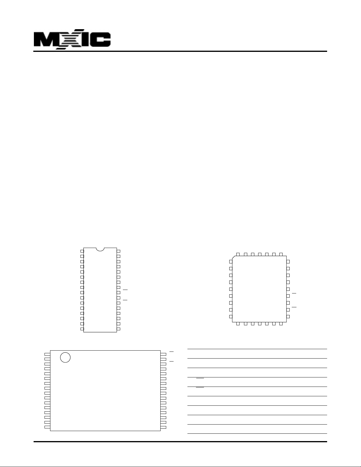
PIN CONFIGURATIONS
32 PDIP/SOP
VCC
32
A18
31
A17
30
A14
29
A13
28
A8
27
A9
26
A11
25
OE
24
A10
23
CE
22
Q7
21
Q6
20
Q5
19
Q4
18
Q3
17
32
31
30
29
28
27
26
25
24
23
22
21
20
19
18
17
32 TSOP
A11
A9
A8
A13
A14
A17
A18
VCC
VPP
A16
A15
A12
A7
A6
A5
A4
VPP
1
A16
2
A15
3
A12
4
A7
5
A6
6
A5
7
A4
8
A3
9
A2
10
A1
A0
Q0
Q1
Q2
GND
1
2
3
4
5
6
7
8
9
10
11
12
13
14
15
16
MX26C4000B
11
12
13
14
15
16
MX26C4000B
TM
OE
A10
CE
Q7
Q6
Q5
Q4
Q3
GND
Q2
Q1
Q0
A0
A1
A2
A3
• Chip erase time: 2s (typ.)
• Chip program time: 25s (typ.)
• 100 minimum erase/program cycles
• Typical fast programming cycle duration 100us/byte
• Package type:
- 32 pin plastic DIP
- 32 pin PLCC
- 32 pin TSOP
- 32 pin SOP
by an EPROM programmer or on-board. The
MX26C4000B supports a intelligent fast programming
algorithm which can result in programming time of less
than one minute.
This MTP EPROMTM is packaged in industry standard 32
pin dual-in-line packages, 32 lead PLCC, 32 lead SOP
and 32 lead TSOP packages.
32 PLCC
A12
A15
A16
VPP
VCC
A18
A17
4
5
A7
A6
A5
A4
9
A3
A2
A1
A0
13
Q0
14 17 20
Q1
PIN DESCRIPTION
SYMBOL PIN NAME
A0~A18 Address Input
Q0~Q7 Data Input/Output
CE Chip Enable Input
OE Output Enable Input
VPP Program Supply Voltage
N C No Internal Connection
VC C Power Supply Pin (+5V)
GN D Ground Pin
1
32
MX26C4000B
Q2
Q3Q4Q5
GND
30
A14
29
A13
A8
A9
A11
25
OE
A10
CE
Q7
21
Q6
P/N: PM0768
1
REV. 0.6, JAN. 14, 2002
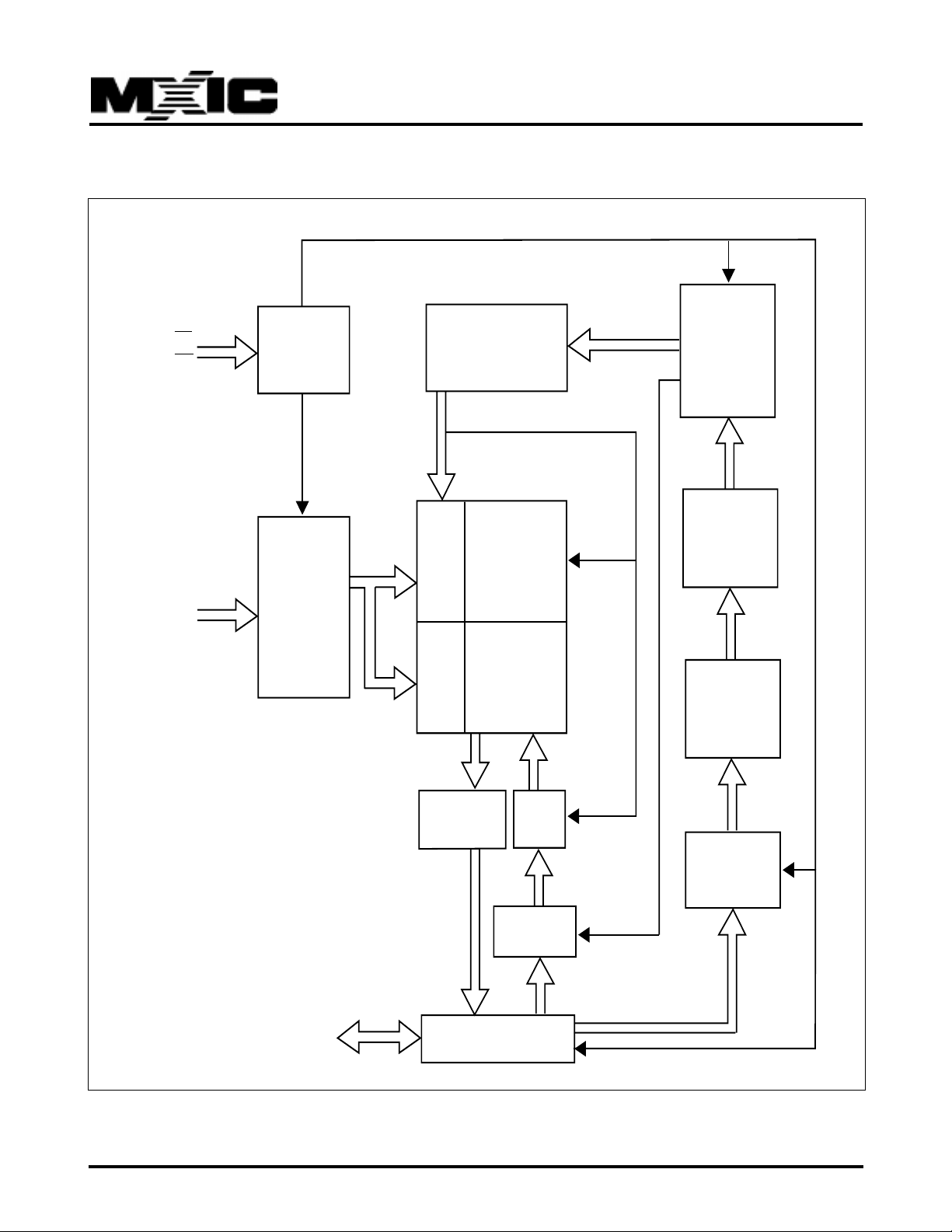
BLOCK DIAGRAM
CE
OE
CONTROL
INPUT
LOGIC
PROGRAM/ERASE
HIGH VOLTA GE
X-DECODER
MX26C4000B
MX26C4000B
WRITE
STATE
MACHINE
(WSM)
STATE
A0-A18
ADDRESS
LATCH
AND
BUFFER
FLASH
ARRA Y
Y-DECODER
Y-PASS GATE
SENSE
AMPLIFIER
DATA LATCH
REGISTER
ARRAY
SOURCE
HV
COMMAND
DATA
DECODER
PGM
DATA
HV
COMMAND
DATA LATCH
PROGRAM
P/N: PM0768
Q0-Q7
I/O BUFFER
2
REV. 0.6, JAN. 14, 2002

MX26C4000B
FUNCTIONAL DESCRIPTION
When the MX26C4000B is delivered, or it is erased, the
chip has all 4M bits in the "ONE", or HIGH state.
"ZEROs" are loaded into the MX26C4000B through the
procedure of programming.
ERASE ALGORITHM
The MX26C4000B do not required preprogramming
before an erase operation. The erase algorithm is a close
loop flow to simultaneously erase all bits in the entire
array. Erase operation starts with the initial erase
operation. Erase verification begins at address 0000H
by reading data FFH from each byte. If any byte fails
to erase. the entire chip is reerased. to a maximum for
10 pulse counts of 500ms duration for each pulse. The
maximum cumulative erase time is 3s. However. the
device is usually erased in no more than 3 pulses. Erase
verification time can be reduced by storing the address
of the last byte that failed. Following the next erase
operation verification may start at the stored address
location. JEDEC standard erase algorithm can also be
used. But erase time will increase by performing the
unnecessary preprogramming.
to the Read Mode. Robust design features prevent
inadvertent write cycles resulting from VCC power-up and
power-down transitions or system noise. To avoid initiation
of write cycle during VCC power-up, a write cycle is locked
out for VCC less than 4V. The two- command program and
erase write sequence to the command register provide
additional software protection against spurious data
changes.
PROGRAM VERIFY MODE
Verification should be performed on the programmed bits
to determine that they were correctly programmed.
Verification should be performed with OE and CE, at
VIL, and VPP at its programming voltage.
ERASE VERIFY MODE
Verification should be performed on the erased chip to
determine that the whole chip(all bits) was correctly
erased. Verification should be performed with OE and
CE at VIL, and VCC = 5V, VPP = 12.5V
AUTO IDENTIFY MODE
PROGRAM ALGORITHM
The device is programmed byte by byte. A maximum
of 25 pulses. each of 100us duration is allowed for each
byte being programmed. The byte may be programmed
sequentially or by random. After each program pulse,
a program verify is done to determine if the byte has
been successfully programmed.
Programming then proceeds to the next desired byte
location. JEDEC standard program algorithms can be
used.
DATA WRITE PROTECTION
The design of the device protects against accidental
erasure or programming. The internal state machine is
automatically reset to the read mode on power-up. Using
control register architecture, alteration of memory can
only occur after completion of proper command
sequences. The command register is only active when V
is at high voltage. when V PP = V
PP
, the device defaults
PPL
The auto identify mode allows the reading out of a binary
code from MTP EPROM that will identify its
manufacturer and device type. This mode is intended
for use by programming equipment for the purpose of
automatically matching the device to be programmed
with its corresponding programming algorithm. This
mode is functional in the 25°C ± 5°C ambient temperature
range that is required when programming the
MX26C4000B.
To activate this mode, the programming equipment must
force 12.0 ± 0.5 V on address line A9 of the device.
Two identifier bytes may then be sequenced from the
device outputs by toggling address line A0 from VIL
to VIH. All other address lines must be held at VIL
during auto identify mode.
Byte 0 ( A0 = VIL) represents the manufacturer code,
and byte 1 (A0 = VIH), the device identifier code. For
the MX26C4000B, these two identifier bytes are given
in the Mode Select Table. All identifiers for manufacturer
and device codes will possess odd parity, with the MSB
(DQ7) defined as the parity bit.
P/N: PM0768
3
REV. 0.6, JAN. 14, 2002

READ MODE
The MX26C4000B has two control functions, both of
which must be logically satisfied in order to obtain data
at the outputs. Chip Enable (CE) is the power control
and should be used for device selection. Output Enable
(OE) is the output control and should be used to gate
data to the output pins, independent of device selection.
Assuming that addresses are stable, address access
time (tACC) is equal to the delay from CE to output (tCE).
Data is available at the outputs tOE after the falling edge
of OE, assuming that CE has been LOW and addresses
have been stable for at least tACC - tOE.
STANDBY MODE
The MX26C4000B has a CMOS standby mode which
reduces the maximum VCC current to 100 uA. It is
placed in CMOS standby when CE is at VCC ± 0.3 V.
The MX26C4000B also has a TTL-standby mode which
reduces the maximum VCC current to 1.5 mA. It is
placed in TTL-standby when CE is at VIH. When in
standby mode, the outputs are in a high-impedance
state, independent of the OE input.
MX26C4000B
SYSTEM CONSIDERATIONS
During the switch between active and standby
conditions, transient current peaks are produced on the
rising and falling edges of Chip Enable. The magnitude
of these transient current peaks is dependent on the
output capacitance loading of the device. At a minimum,
a 0.1 uF ceramic capacitor (high frequency, low inherent
inductance) should be used on each device between
VCC and GND to minimize transient effects. In addition,
to overcome the voltage drop caused by the inductive
effects of the printed circuit board traces on EPROM
arrays, a 4.7 uF bulk electrolytic capacitor should be
used between VCC and GND for each of the eight
devices. The location of the capacitor should be close
to where the power supply is connected to the array.
OUTPUT DISABLE
Output is disabled when OE is at logre high. When in
output disabled all circuitry is enabled. Except the output
pins are in a high impedance state(Hi-Z).
P/N: PM0768
4
REV. 0.6, JAN. 14, 2002
MX26C4000B
Table 1: BUS OPERATIONS
Mode VPP(1) A0 A9 CE OE Q0~Q7
Read VPPL A0 A9 VIL VIL Data Out
Output Disable VPPL X X VIL VIH Hi-Z
Standby VPPL X X VIH X Hi-Z
Manufacturer Identification VPPL VIL VID(2) VIL VIL Data=C2H
Device Identification VPPL VIH VID(2) VIL VIL Data=C0H
Program VPPH A0 X VIL VIH Data In
Verify VPPH A0 X VIH VIL Data Out
Program Inhibit VPPH X X VIH VIH Hi-Z
Note:
1. Refer to DC Characteristics. When VPP=VPPL memory contents can be read but not written or erased.
2. VID is the intelligent identifier high voltage. Refer to DC Characteristics.
3. Read operations with VPP=VPPH may access array data or the intelligent identifier codes.
4. With VPP at high voltage the standby current equals ICC+IPP(standby).
5. Refer to Table 2 for vaild data-in during a write operation.
6. X can be VIL or VIH.
P/N: PM0768
5
REV. 0.6, JAN. 14, 2002
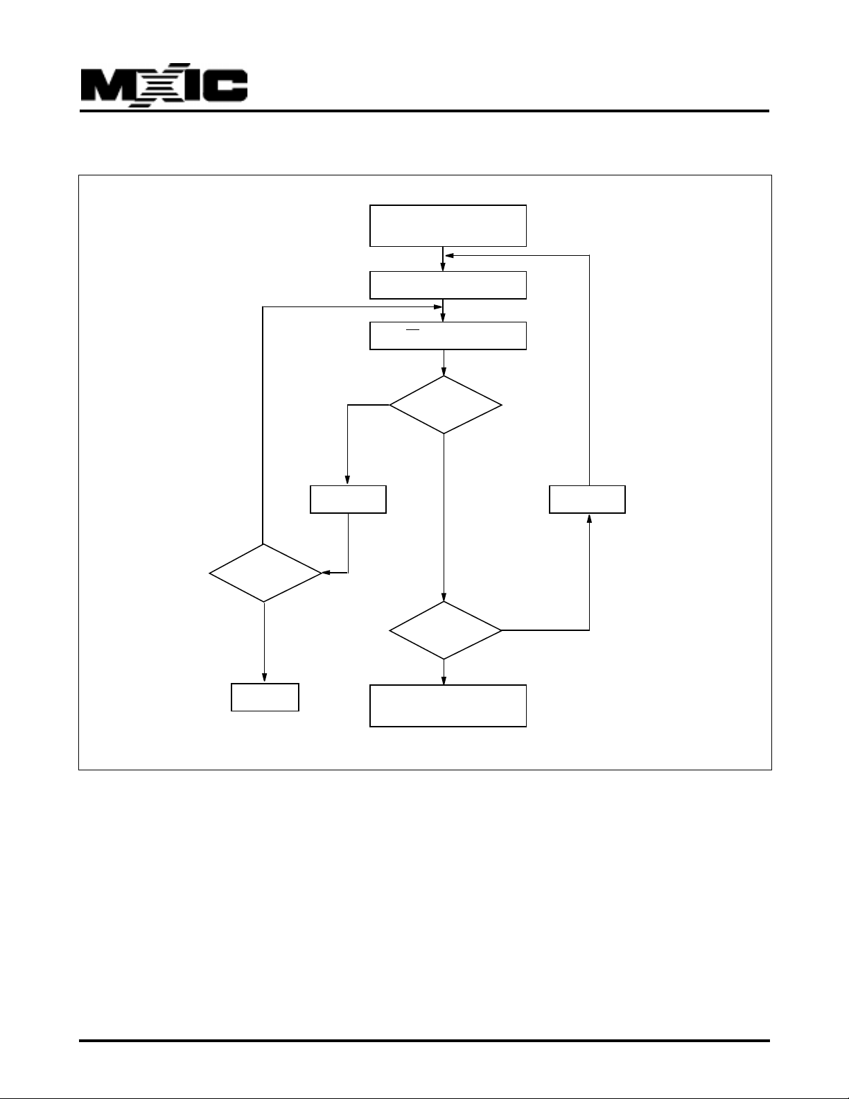
PROGRAMMING ALGORITHM FLOW CHART
NO
MX26C4000B
VCC=6.25V
VPP=12.75V
n=0
CE=100us Pulse
Verify
n=25
Failed
NO
YES
N=N+1
YES
Last
Address
YES
Check All Bytes
1st:VCC=6V
2nd:VCC=4.2V
next
Address
NO
P/N: PM0768
6
REV. 0.6, JAN. 14, 2002
 Loading...