


MXIC MX23L12810MC-13, MX23L12810MC-90, MX23L12810MC-15, MX23L12810MC-10, MX23L12810MC-12 Datasheet
1
P/N:PM0750 REV. 1.3, AUG. 28, 2001
FEATURES
• Bit organization
- 8M x 16 (word mode)
• Fast access time
- Random access: 90ns (max.)
• Current
- Operating:50mA
- Standby:15uA
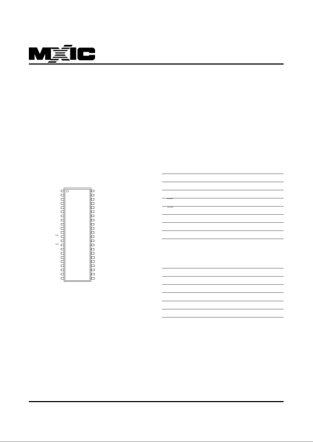
PIN CONFIGURATION
44 SOP(For Word Mode Only)
MX23L12810
• Supply voltage
- 3.0~3.6V
• Package
- 44 pin SOP (500mil)
• Temperature
- 0 ~ 70°C
128M-BIT (8M x 16) MASK ROM
(SOP ONLY)
PIN DESCRIPTION
Symbol Pin Function
A0~A22 Address Inputs
D0~D15 Data Outputs
CE Chip Enable Input
OE Output Enable Input
VC C Pow er Supply Pin
VSS Ground Pin
N C No Connection
ORDER INFORMATION
Part No. Access Time Package
MX23L12810MC-90 90ns 44 pin SOP
MX23L12810MC-10 100ns 44 pin SOP
MX23L12810MC-12 120ns 44 pin SOP
MX23L12810MC-13 130ns 44 pin SOP
MX23L12810MC-15 150ns 44 pin SOP
2
3
4
5
6
7
8
9
10
11
12
13
14
15
16
17
18
19
20
21
22
44
43
42
41
40
39
38
37
36
35
34
33
32
31
30
29
28
27
26
25
24
23
A21
A18
A17
A7
A6
A5
A4
A3
A2
A1
A0
CE
VSS
OE
D0
D8
D1
D9
D2
D10
D3
D11
A20
A19
A8
A9
A10
A11
A12
A13
A14
A15
A16
A22
VSS
D15
D7
D14
D6
D13
D5
D12
D4
VCC
MX23L12810
2
P/N:PM0750
REV. 1.3, AUG. 28, 2001
MX23L12810
ABSOLUTE MAXIMUM RATINGS
Item Symbol Ratings
V oltage on any Pin Relative to VSS VIN -1.3V to VCC+2.0V (Note)
Ambient Operating Temperature Topr 0°C to 70°C
Storage T emperature Tstg -65°C to 125°C
DC CHARACTERISTICS (Ta = 0°C ~ 70°C, VCC = 3.0V~3.6V)
Item Symbol MIN. MAX. Conditions
Output High V oltage V OH 2.4V - IOH = -0.4mA
Output Low V oltage V OL - 0.4V IOL = 1.6mA
Input High V oltage VIH 2.2V VCC+0.3V
Input Low Voltage VIL -0.3V 0.2 x VCC
Input Leakage Current ILI - 5u A 0V , VCC
Output Leakage Current ILO - 5uA 0V , VCC
Operating Current ICC1 - 50mA f=5MHz, all outputs open
Standby Current (TTL) ISTB1 - 1mA CE = VIH
Standby Current (CMOS) ISTB2 - 15uA CE>VCC-0.2V
Input Capacitance CIN - 10pF Ta = 25°C, f = 1MHZ
Output Capacitance COUT - 10pF T a = 25°C, f = 1MHZ
Note: Minimum DC v oltage on input or I/O pins is -0.5V.
During voltage transitions, inputs may undershoot VSS
to -1.3V for periods of up to 20ns. Maximum DC voltage
on input or I/O pins is VCC+0.5V. During v oltage transitions, inputs may o vershoot VCC to VCC+2.0V for periods of up to 20ns.
Note: Output high-impedance dela y (tHZ) is measured
from OE or CE going high, and this parameter guaranteed by design over the full voltage and temperature
operating range - not tested.
AC CHARACTERISTICS (Ta = 0°C ~ 70°C, VCC = 3.0V~3.6V)
Item Symbol 23L12810-90 23L12810-10 23L12810-12 23L12810-13 23L12810-15
MIN. MAX. MIN. MAX. MIN. MAX. MIN. MAX. MIN. MAX.
Read Cycle Time tR C 90ns - 100ns - 120ns - 130ns - 150ns Address Access Time tAA - 90ns - 100ns - 120ns - 130ns - 150ns
Chip Enable Access Time tACE - 90ns - 100ns - 120ns - 130ns - 150ns
Output Enable Time tOE - 25ns - 30ns - 50ns - 50ns - 70ns
Output Hold After Address t OH 0ns - 0ns - 0ns - 0ns - 0n s Output High Z Delay tHZ - 20ns - 20ns - 20ns - 20ns - 20ns
 Loading...