


Motorola MC74LVQ646DT, MC74LVQ646DW, MC74LVQ646SD Datasheet
SEMICONDUCTOR TECHNICAL DATA
1
REV 0
Motorola, Inc. 1995
12/95
%" #"
" !$ !"
!$
"" $ "
The MC74LVQ646 is a high performance, non–inverting octal
transceiver/registered transceiver operating from a 2.7 to 3.6V supply.
High impedance TTL compatible inputs significantly reduce current
loading to input drivers while TTL compatible outputs offer improved
switching noise performance. The MC74LVQ646 is suitable for memory
address driving and all TTL level bus oriented transceiver applications.
Data on the A or B bus will be clocked into the registers as the
appropriate clock pin goes from a LOW–to–HIGH logic level. Output
Enable (OE
) and DIR pins are provided to control the transceiver outputs.
In the transceiver mode, data present at the high impedance port may be
stored in either the A or the B register or in both. The select controls (SBA,
SAB) can multiplex stored and real–time (transparent mode) data. The
direction control (DIR) determines which bus will receive data when the
enable OE
is active LOW. In the isolation mode (OE HIGH), A data may
be stored in the B register or B data may be stored in the A register. Only
one of the two buses, A or B, may be driven at one time.
• Designed for 2.7 to 3.6V V
CC
Operation – Ideal for Low Power/Low
Noise Applications
• Guaranteed Simultaneous Switching Noise Level and Dynamic
Threshold Performance
• Guaranteed Skew Specifications
• Guaranteed Incident Wave Switching into 75Ω
• Low Static Supply Current (10µA) Substantially Reduces System Power
Requirements
• Latchup Performance Exceeds 500mA
• ESD Performance: Human Body Model >2000V
Pinout: 24–Lead Package (Top View)
2324 22 21 20 19 18
21 3 4 5 6 7
V
CC
17
8
16
9
15
10
CBA SBA OE
B0 B1 B2 B3 B4 B5
CAB SAB DIR A0 A1 A2 A3 A4 A5 A6
14
11
13
12
B6 B7
A7 GND
LVQ
DW SUFFIX
PLASTIC SOIC
CASE 751E–04
DT SUFFIX
PLASTIC TSSOP
CASE 948H–01
24
1
24
1
SD SUFFIX
PLASTIC SSOP
CASE 940D–03
24
1
LOW–VOLTAGE CMOS
OCTAL TRANSCEIVER/
REGISTERED TRANSCEIVER
PIN NAMES
Function
Side A Inputs/Outputs
Side B Inputs/Outputs
Clock Pulse Inputs
Select Control Inputs
Output Enable Inputs
Pins
A0–A7
B0–B7
CAB, CBA
SAB, SBA
DIR, OE
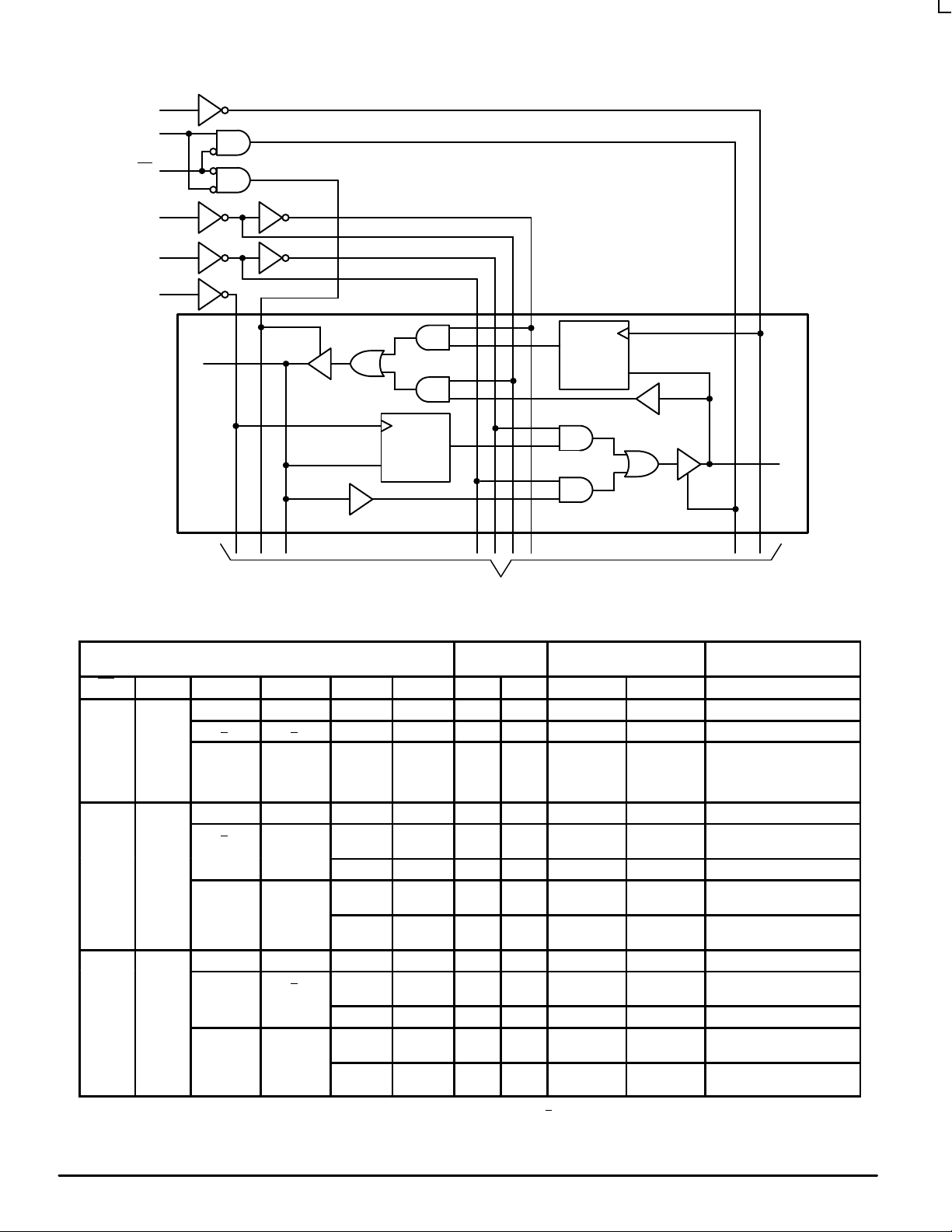
LOGIC DIAGRAM
C
D
Q
OE
DIR
CBA
SBA
SAB
CAB
C
D
Q
A0
B0
1 of 8 Channels
To 7 Other Channels
1
3
21
22
2
23
MC74LVQ646
MOTOROLA LVQ DATA
BR1478
2
FUNCTION TABLE
Inputs
Storage
Registers
Data
Ports
Operating Mode
OE DIR CAB CBA SAB SBA QA QB An Bn Operating Mode
H X Input Input
↑ ↑ X X NC NC X X Isolation, Hold Storage
↑ ↑ X X L
H
X
X
X
X
L
H
L
H
X
X
X
X
L
H
Store A and/or B Data
L H Input Output
↑ X* L X NCNCNC
NC
L
H
L
H
Real Time A Data to B Bus
H X NC NC X QA Stored A Data to B Bus
↑ X* L X L
H
NC
NC
L
H
L
H
Real Time A Data to B Bus;
Store A Data
H X L
H
NC
NC
L
H
QA
QA
Stored A Data to B Bus;
Store A Data
L L Output Input
X* ↑ X L NCNCNC
NC
L
H
L
H
Real Time B Data to A Bus
X H NC NC QB X Stored B Data to A Bus
X* ↑ X L NC
NC
L
H
L
H
L
H
Real Time B Data to A Bus;
Store B Data
X H NC
NC
L
H
QB
QB
L
H
Stored B Data to A Bus;
Store B Data
H = High Voltage Level; L = Low V oltage Level; X = Don’t Care; ↑ = Low–to–High Clock T ransition; ↑ = NOT Low–to–High Clock Transition; NC = No Change; * = The
clocks are not internally gated with either the Output Enables or the Source Inputs. Therefore, data at the A or B ports may be clocked into the storage registers, at any
time. For ICC reasons, Do Not Float Inputs.
MC74LVQ646
LCX DATA
BR1478
3 MOTOROLA
BUS APPLICATIONS
BUS A
BUS B
OELDIRLCABXCBAXSABXSBA
L
Real Time Transfer – Bus B to
Bus A
BUS A
BUS B
OELDIRHCABXCBAXSABLSBA
X
Real Time Transfer – Bus A to
Bus B
BUS B
OE
X
X
H
DIR
X
X
X
CAB
↑
X
↑
CBA
X
↑
↑
SAB
X
X
X
SBA
X
X
X
Store Data from Bus A, Bus B or
Busses A and B
BUS A
BUS B
OE
L
L
DIR
L
H
CAB
X
H or L
CBA
H or L
X
SAB
X
H
SBA
H
X
Transfer Storage Data to Bus A
or Bus B
BUS A
 Loading...