


Motorola MC74LVQ574SD, MC74LVQ574DT, MC74LVQ574DW, MC74LVQ574M Datasheet
SEMICONDUCTOR TECHNICAL DATA
1
REV 0
Motorola, Inc. 1995
11/95
!'!$ %$
$ (" "!"
!' #!% !%$
$$ ! &#$
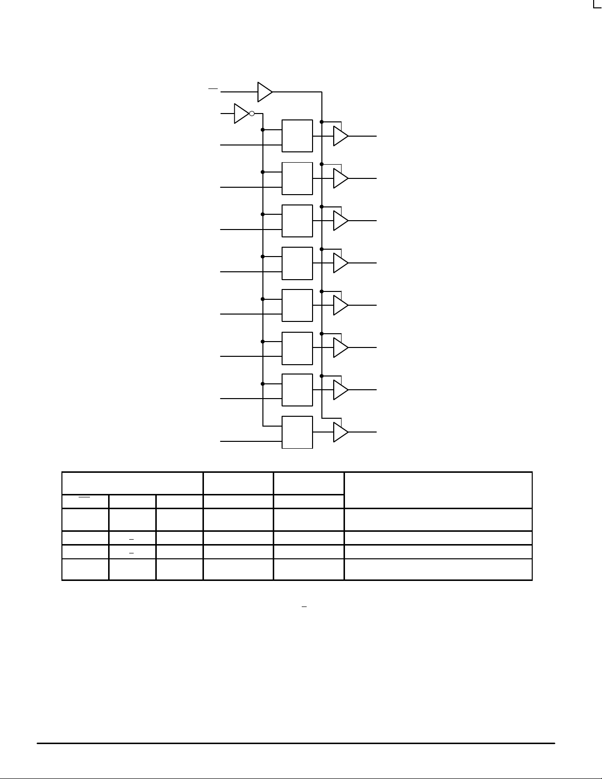
The MC74LVQ574 is a high performance, non–inverting octal D–type
flip–flop operating from a 2.7 to 3.6V supply. The MC74LVQ574 is
suitable for TTL level bus oriented applications where a memory element
is required.
Current drive capability is 12mA at the outputs. The MC74LVQ574
consists of 8 edge–triggered flip–flops with individual D–type inputs and
3–state true outputs. The buffered clock and buffered Output Enable (OE
)
are common to all flip–flops. The eight flip–flops will store the state of
individual D inputs that meet the setup and hold time requirements on the
LOW–to–HIGH Clock (CP) transition. With the OE
LOW, the contents of
the eight flip–flops are available at the outputs. When the OE
is HIGH, the
outputs go to the high impedance state. The OE
input level does not affect
the operation of the flip–flops.
• Designed for 2.7 to 3.6V V
CC
Operation – Ideal for Low Power/Low
Noise Applications
• Guaranteed Simultaneous Switching Noise Level and Dynamic
Threshold Performance
• Guaranteed Skew Specifications
• Guaranteed Incident Wave Switching into 75Ω
• Low Static Supply Current (10µA) Substantially Reduces System Power
Requirements
• Latchup Performance Exceeds 500mA
• ESD Performance: Human Body Model >2000V
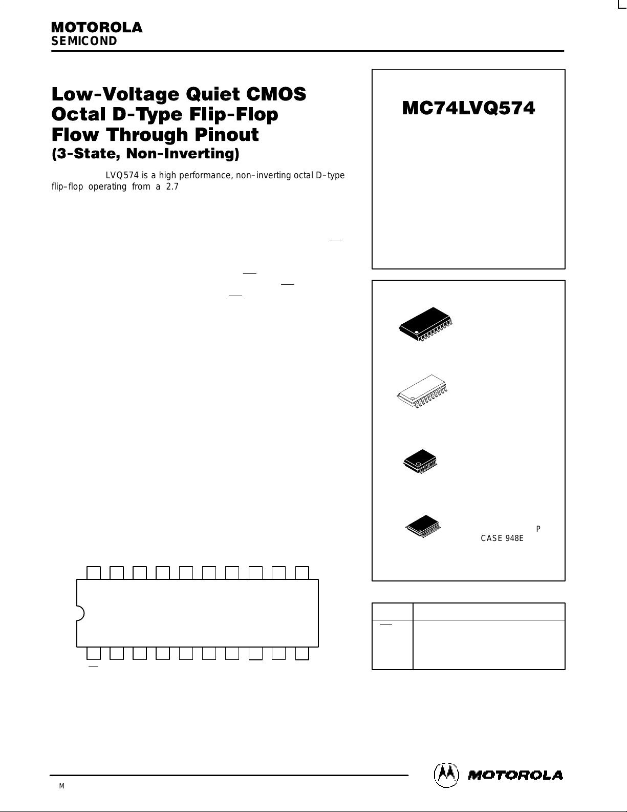
Pinout: 20–Lead (Top View)
1920 18 17 16 15 14
21 3 4 5 6 7
V
CC
13
8
12
9
11
10
O0 O1 O2 O3 O4 O5 O6 O7 CP
OE
D0 D1 D2 D3 D4 D5 D6 D7 GND
LOW–VOLTAGE CMOS
OCTAL D–TYPE FLIP–FLOP
LVQ
DW SUFFIX
PLASTIC SOIC
CASE 751D–04
DT SUFFIX
PLASTIC TSSOP
CASE 948E–02
20
1
20
1
M SUFFIX
PLASTIC SOIC EIAJ
CASE 967–01
20
1
SD SUFFIX
PLASTIC SSOP
CASE 940C–03
20
1
PIN NAMES
Function
Output Enable Input
Clock Pulse Input
Data Inputs
3–State Outputs
Pins
OE
CP
D0–D7
O0–O7
MC74LVQ574
MOTOROLA ECLinPS and ECLinPS Lite
DL140 — Rev 3
2
O0
D0
O1
D1
O2
D2
O3
D3
O4
D4
O5
D5
O6
D6
O7
D7
LOGIC DIAGRAM
nCP
Q
D
nCP
Q
D
nCP
Q
D
nCP
Q
D
nCP
Q
D
nCP
Q
D
nCP
Q
D
nCP
Q
D
CP
OE
11
1
2
3
4
5
6
7
8
9
19
18
17
16
15
14
13
12
INPUTS
INTERNAL
LATCHES
OUTPUTS
OE CP Dn Q On
OPERATING MODE
L
L
↑
↑
l
h
L
H
L
H
Load and Read Register
L ↑ X NC NC Hold and Read Register
H ↑ X NC Z Hold and Disable Outputs
H
H
↑
↑
l
h
L
H
Z
Z
Load Internal Register and Disable Outputs
H = High Voltage Level; h = High V oltage Level One Setup T ime Prior to the Low–to–High Clock Transition; L = Low Voltage Level; l = Low
Voltage Level One Setup T ime Prior to the Low–to–High Clock Transition; NC = No Change; X = High or Low V oltage Level and T ransitions
are Acceptable; Z = High Impedance State; ↑ = Low–to–High Transition; ↑
= Not a Low–to–High Transition; For ICC Reasons DO NOT FLOAT
Inputs
MC74LVQ574
ECLinPS and ECLinPS Lite
DL140 — Rev 3
3 MOTOROLA
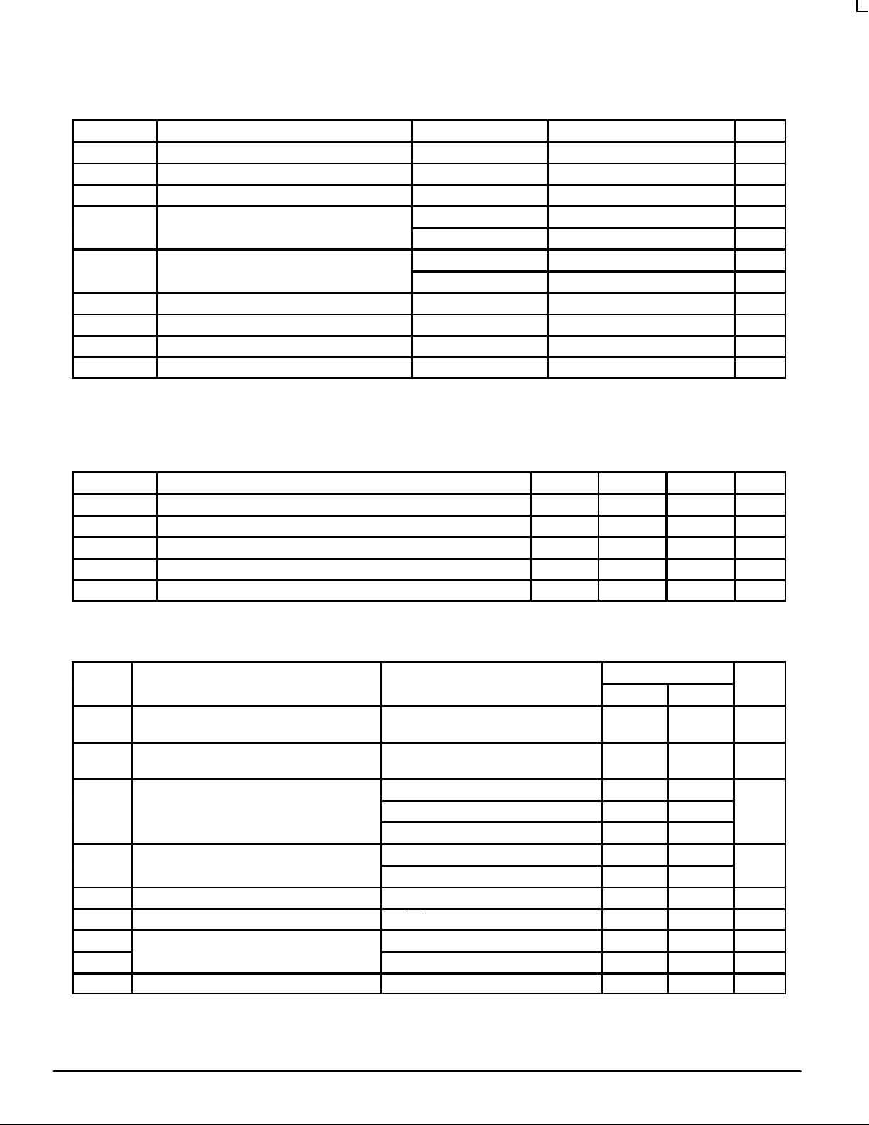
ABSOLUTE MAXIMUM RATINGS*
Symbol Parameter Value Condition Unit
V
CC
DC Supply Voltage –0.5 to +7.0 V
V
I
DC Input Voltage –0.5 ≤ VI ≤ VCC + 0.5V V
V
O
DC Output Voltage –0.5 ≤ VO ≤ VCC + 0.5 Output in HIGH or LOW State V
I
IK
DC Input Diode Current –20 VI = –0.5V mA
+20 VI = VCC + 0.5V mA
I
OK
DC Output Diode Current –20 VO = –0.5V mA
+20 VI = VCC + 0.5V mA
I
O
DC Output Source/Sink Current ±50 mA
I
CC
DC Supply Current ±400 mA
I
GND
DC Ground Current ±400 mA
T
STG
Storage Temperature Range –65 to +150 °C
* Absolute maximum continuous ratings are those values beyond which damage to the device may occur. Exposure to these conditions or
conditions beyond those indicated may adversely affect device reliability. Functional operation under absolute–maximum–rated conditions is
not implied.
RECOMMENDED OPERATING CONDITIONS
Symbol Parameter Min Typ Max Unit
V
CC
Supply Voltage 2.0 3.3 3.6 V
V
I
Input Voltage 0 V
CC
V
V
O
Output Voltage 0 V
CC
V
T
A
Operating Free–Air Temperature –40 +85 °C
∆V/∆t Input Transition Rise or Fall Rate, VIN from 0.8V to 2.0V, VCC = 3.0V 0 125 mV/ns
DC ELECTRICAL CHARACTERISTICS
TA = –40°C to +85°C
Symbol Characteristic Condition Min Max Unit
V
IH
HIGH Level Input Voltage (Note 1) 2.7V ≤ VCC ≤ 3.6V,
VO = 0.1V or VCC – 0.1V
2.0 V
V
IL
LOW Level Input Voltage (Note 1) 2.7V ≤ VCC ≤ 3.6V,
VO = 0.1V or VCC – 0.1V
0.8 V
V
OH
HIGH Level Output Voltage 2.7V ≤ VCC ≤ 3.6V; IOH = –50µA VCC– 0.1 V
VCC = 2.7V; IOH = –12mA 2.2
VCC = 3.0V; IOH = –12mA 2.48
V
OL
LOW Level Output Voltage 2.7V ≤ VCC ≤ 3.6V; IOL = 50µA 0.1 V
2.7V ≤ VCC ≤ 3.6V; IOL= 12mA 0.4
I
I
Input Leakage Current 2.7V ≤ VCC ≤3.6V; VI= VCC, GND ±1.0 µA
I
OZ
Maximum 3–State Leakage Current VI(OE) = VIL, VIH; VI, VO= VCC, GND ±2.5 µA
I
OLD
Minimum Dynamic Output Current (Note 2) VCC = 3.6V; V
OLD
= 0.8V Max 36 mA
I
OHD
VCC = 3.6V; V
OHD
= 2.0V Min –25 mA
I
CC
Quiescent Supply Current 2.7V ≤ VCC ≤3.6V; VI = VCC, GND 10 µA
1. These values of VI are used to test DC electrical characteristics only. Functional test should use VIH ≥ 2.4V, VIL ≤ 0.5V.
2. Incident wave switching on transmission lines with impedances as low as 75Ω for commercial temperature range is guaranteed. Maximum test
duration is 2ms, one output loaded at a time.
 Loading...