

Motorola MC74F1803D, MC74F1803N Datasheet
Order this document
from Logic Marketing
SEMICONDUCTOR TECHNICAL DATA
Motorola, Inc. 1995
1
7/95
REV 4
!%!
$ &
# # ! # &"
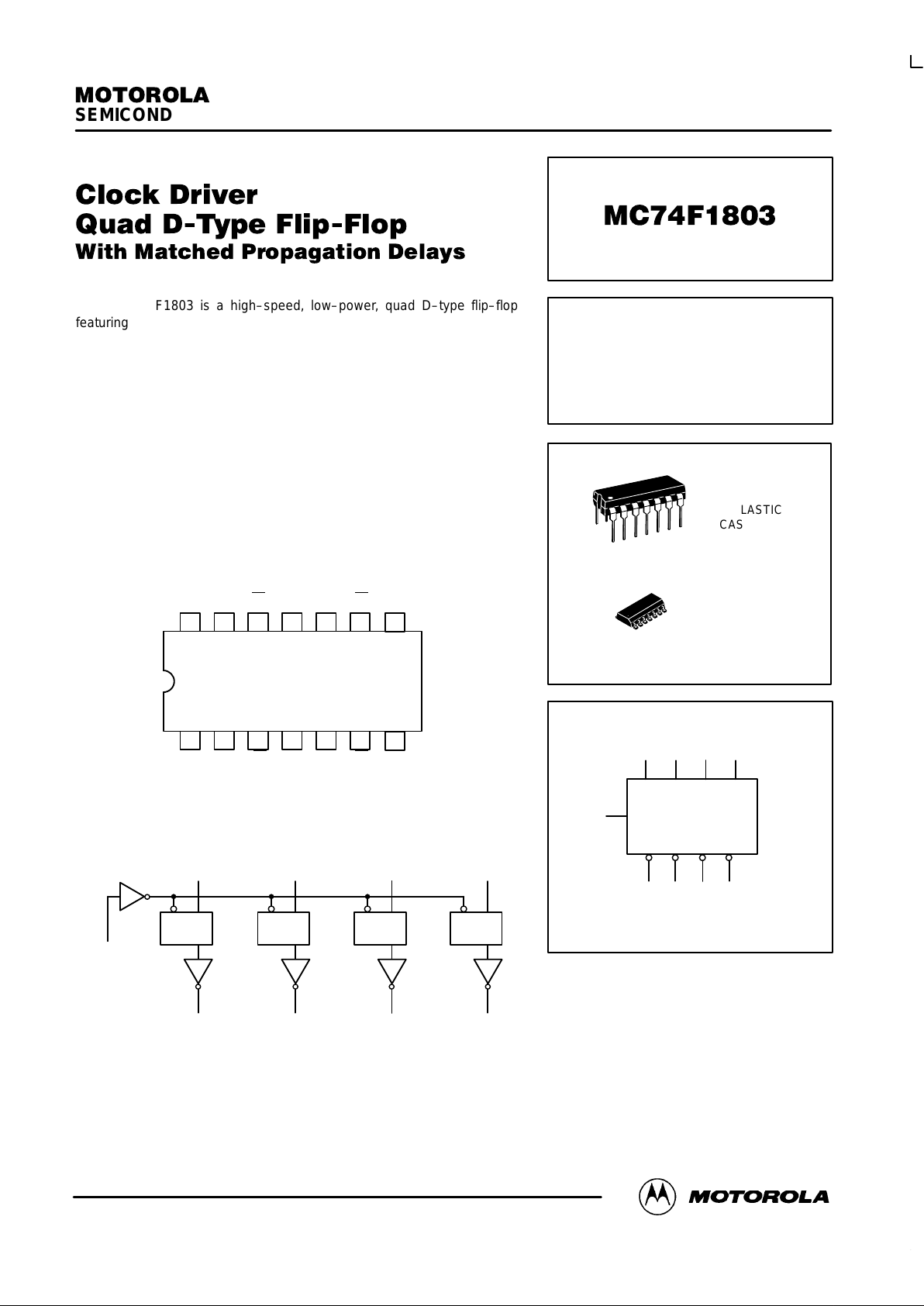
The MC74F1803 is a high–speed, low–power, quad D–type flip–flop
featuring separate D–type inputs and inverting outputs with closely matched
propagation delays. With a buffered clock (CP) input that is common to all
flip–flops, the MC74F1803 is useful in high–frequency systems as a clock
driver, providing multiple outputs that are synchronous. Because of the
matched propagation delays, the duty cycles of the output waveforms in a
clock driver application are symmetrical within 2.0 nanoseconds.
• Edge–Triggered D–Type Inputs
• Buffered Positive Edge–Triggered Clock
• Matched Outputs for Synchronous Clock Driver Applications
• Outputs Guaranteed for Simultaneous Switching
Pinout: 14–Lead Plastic (Top View)
14 13 12 11 10 9
123456
8
7
VCCNC O
3D3D2O2
CP
GND NC O
0
D0D1O1GND
LOGIC DIAGRAM
CP
D0
CP D
Q
O
0
D1
CP D
Q
O
1
D2
CP D
Q
O
2
D3
CP D
Q
O
3
VCC = Pin 14; GND = Pins 1,7; NC = Pins 2, 13
NOTE: This diagram is provided only for the understanding of logic operations and
should not be used to estimate propagation delays
CLOCK DRIVER QUAD
D–TYPE FLIP–FLOP WITH
MATCHED PROPAGATION
DELAYS
N SUFFIX
PLASTIC
CASE 646–06
14
1
14
1
D SUFFIX
SOIC
CASE 751A–03
LOGIC SYMBOL
8
451011
36912
D0 D1 D2 D3
O1O0 O2 O3
CP
VCC = PIN 14
GND = PINS 1 AND 7
NC = PINS 2 AND 13
MC74F1803
MOTOROLA TIMING SOLUTIONS
BR1333 — REV 5
2
FUNCTIONAL DESCRIPTION
The MC74F1803 consists of four positive edge–triggered
flip–flops with individual D–type inputs and inverting
outputs. The buffered clock is common to all flip–flops
and the following specifications allow for outputs switching
simultaneously. The four flip–flops store the state of their
individual D inputs that meet the setup and hold time
requirements on the LOW–to–HIGH Clock (CP) transition.
The maximum frequency of the clock input is
70 megahertz and the LOW–to–HIGH and HIGH–to–LOW
propagation delays of the On
output vary by at most,
2.0 nanoseconds. Therefore, the device is ideal for use as
a divide–by–two driver for high–frequency clock signals
that require symmetrical duty cycles. In addition, the
output–to–output skew is a maximum of 2.0 nanoseconds.
Finally, the IOH specification at 2.5 volts is guaranteed to
be at least –20 milli–amps. If their inputs are identical,
multiple outputs can be tied together and the IOH is
commensurately increased.
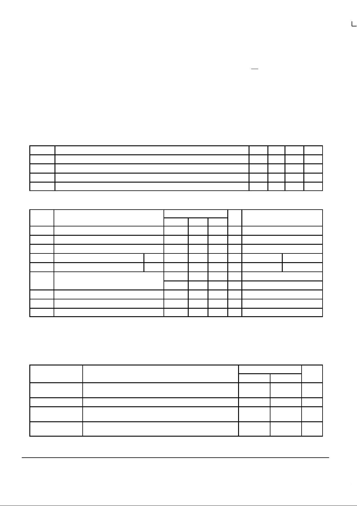
GUARANTEED OPERATION RANGES
Symbol Parameter Min Typ Max Unit
V
CC
Supply Voltage 4.5 5.0 5.5 V
T
A
Operating Ambient Temperature Range 0 25 70 °C
I
OH
Output Current — High — — –20 mA
I
OL
Output Current — Low — — 24 mA
DC CHARACTERISTICS OVER OPERATING TEMPERATURE RANGE (Unless otherwise specified)
Limits
Symbol Parameter Min Typ Max Unit Test Conditions
1,2
V
IH
Input HIGH Voltage 2.0 – – V Guaranteed Input HIGH Voltage
V
IL
Input LOW Voltage – – 0.8 V Guaranteed Input LOW Voltage
V
IK
Input Clamp Diode Voltage – – –1.2 V VCC = MIN, IIN = –18 mA
V
OH
Output HIGH Voltage An Outputs 74 2.5 – – V IOH = –20 mA VCC =4.5 V
V
OL
Output LOW Voltage An
Outputs
74 – 0.35 0.5 V IOL = 24 mA VCC = MIN
I
IH
Input HIGH Current – – 20 µA VCC = MAX, VIN = 2.7 V
– – 100 µA VCC = MAX, VIN = 7.0 V
I
IL
Input LOW Current – – –0.6 mA VCC = MAX, VIN = 0.5 V
I
OS
Output Short Circuit Current
3
–60 – –150 mA VCC = MAX, V
OUT
= 0 V
I
CC
Power Supply Current – – 70 mA VCC = MAX
1. For conditions shown as MIN or MAX, use the appropriate value specified under recommended operating conditions for the applicable device
type.
2. Normal test conditions for this device are all four outputs switching simultaneously. Two outputs of the MC74F1803 can be tied together and
the IOH doubles.
3. Not more than one output should be shorted at a time, nor for more than 1 second.
AC OPERATING REQUIREMENTS (T
A
= 0°C to +70°C: VCC = +5.0 V ±10%: RL = 500 Ω)
CL = 50 pF
Symbol Parameter Min Max Unit
ts(H)
ts(L)
Setup Time, HIGH or LOW: Dn to CP 3.0
3.0
–
–
ns
t
f
tp + ts
1
– 9.0 ns
th(H)
th(L)
Hold Time, HIGH or LOW: Dn to CP 2.0
2.0
–
–
ns
tw(H)
tw(L)
Cp Pulse Width HIGH or LOW 7.0
6.0
–
–
ns
1. The combination of the setup time (ts) requirement and maximum propagation delay (tp) are guaranteed to be within this limit for all conditions.
 Loading...