

Motorola MC100LVEL92, MC100LVEL92DW, MC100LVEL92DWR2 Datasheet

SEMICONDUCTOR TECHNICAL DATA
The MC100L VEL92 is a triple PECL to L VPECL translator. The device
receives standard PECL signals and translates them to differential
LVPECL output signals.
• 500ps Propagation Delays
• Fully Dif ferential Design
• 20–Lead SOIC Package
• 5V and 3.3V Supplies Required
• >1500V ESD
A PECL VBB output is provided for interfacing single ended PECL
signals at the inputs. If a single ended PECL input is to be used the PECL
VBB output should be connected to the D
drive the D input. When used the PECL VBB should be bypassed to
ground via a 0.01µf capacitor. The PECL VBB is designed to act as a
switching reference for the MC100LVEL92 under single ended input
conditions, as a result the pin can only source/sink 0.5mA of current.
To accomplish the PECL to LVPECL level translation, the
MC100LVEL92 requires three power rails. The VCC supply is to be
connected to the standard PECL supply, the LVCC supply is to be
connected to the L VPECL supply , and Ground is connected to the system
ground plane. Both the VCC and LVCC should be bypassed to ground
with a 0.01µf capacitor.
Under open input conditions, the D
voltage level and the D input will be pulled to ground. This condition will
force the “Q” output low, ensuring stability.
Logic Diagram and Pinout: 20-Lead SOIC (Top View)
input and the active signal will
input will be biased at a VCC/2
20
1
DW SUFFIX
PLASTIC SOIC PACKAGE
CASE 751D-04
PIN NAMES
Pins
Dn
Qn
V
BB
LVCC
V
CC
GND
Function
PECL Inputs
LVPECL Outputs
PECL Reference Voltage Output
VCC for LVPECL Output
VCC for PECL Inputs
Common Ground Rail
VCCQ0
LVPECL
PECL
CC
7/97
Motorola, Inc. 1997
1920
21
D0
Q1 Q1 Q2 Q2 V
LVCC
Q0
1718 16 15 14 13 12
LVPECL
PECL
56789
43
PECL
V
BB
D1
D0 D2V
LVCC
LVPECL
PECL
V
4–1
PECL
BB
CC
11
10
D2D1
GND
REV 2
MC100LVEL92
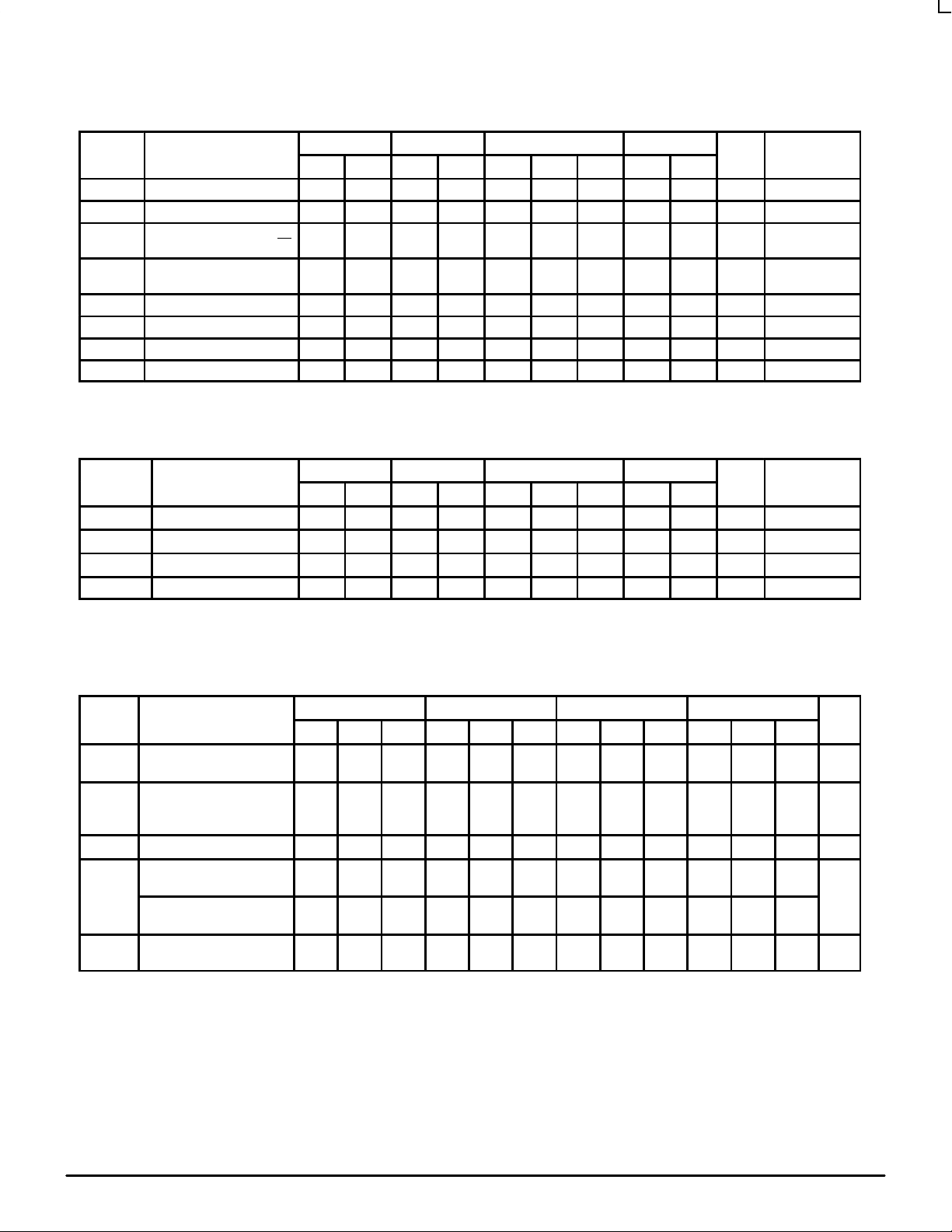
PECL INPUT DC CHARACTERISTICS
–40°C 0°C 25°C 85°C
Symbol Characteristic Min Max Min Max Min Typ Max Min Max Unit Condition
V
CC
I
IH
I
IL
V
PP
V
IH
V
IL
V
BB
I
VCC
1. 150mV input guarantees full logic swing at the output.
2. DC levels vary 1:1 with VCC.
LVPECL OUTPUT DC CHARACTERISTICS
Symbol Characteristic Min Max Min Max Min Typ Max Min Max Unit Condition
V
CC
V
OH
V
OL
I
GND
3. DC levels will vary 1:1 with VCC.
Power Supply Voltage 4.5 5.5 4.5 5.5 4.5 5.5 4.5 5.5 V
Input HIGH Current 150 150 150 150 µA
Input LOW Current DnDn0.5
Minimum Peak-to-Peak
1
Input
Input HIGH Voltage
Input LOW Voltage
Reference Output
Power Supply Current 12 12 8.0 12 12 mA
2
2
2
–600
150 150 150 150 mV
3835 4120 3835 4120 3835 4120 3835 4120 mV VCC = 5.0V
3190 3515 3190 3525 3190 3525 3190 3525 mV VCC = 5.0V
3620 3740 3620 3740 3620 3740 3620 3740 mV VCC = 5.0V
0.5
–600
0.5
–600
0.5
–600
µA
–40°C 0°C 25°C 85°C
Power Supply Voltage 3.0 3.8 3.0 3.8 3.0 3.3 3.8 3.0 3.8 V
Output HIGH Voltage32.215 2.42 2.275 2.42 2.275 2.35 2.42 2.275 2.42 V VCC = 3.3V
Output LOW Voltage
3
1.47 1.745 1.49 1.68 1.49 1.60 1.68 1.49 1.68 V VCC = 3.3V
Power Supply Current 20 20 15 20 21 mA
MC100LVEL92
AC CHARACTERISTICS (LVCC = 3.0V to 3.8V; VCC = 4.5V to 5.5V)
–40°C 0°C 25°C 85°C
Symbol Characteristic Min Typ Max Min Typ Max Min Typ Max Min Typ Max Unit
t
PLH
t
PHL
t
SKEW
V
PP
V
CMR
t
r
t
f
4. Skews are valid across specified voltage range, part–to–part skew is for a given temperature.
5. Duty cycle skew is the difference between a TPLH and TPHL propagation delay through a device.Common Mode Range
6. Minimum input swing for which AC parameters guaranteed. The device has a DC gain of ≈40.
7. The CMR range is referenced to the most positive side of the differential input signal. Normal operation is obtained if the HIGH level falls within
the specified range and the peak-to-peak voltage lies between VPPmin and 1V .
Propagation Delay Diff
D to Q S.E.
Skew Output–to–Output
Part–to–Part (Diff)
Duty Cycle (Diff)
Minimum Input Swing
Common Mode Range
6
7
VPP < 500mV
VPP ≥ 500mV 1.5
Output Rise/Fall Times Q
(20% – 80%)
490
590
690
510
610
710
510
610
710
530
440
590
740
460
610
760
460
610
760
4
4
5
20
20
25
100
200
20
20
25
100
200
20
20
25
100
200
480
630
630
20
20
25
150 150 150 150 mV
1.3
V
CC
–0.2
V
CC
–0.2
1.2
1.4
V
CC
–0.2
V
CC
–0.2
1.2
1.4
V
CC
–0.2
V
CC
–0.2
1.2
1.4
320 580 320 580 320 580 320 580 ps
730
780
100
200
V
CC
–0.2
V
CC
–0.2
ps
ps
V
MOTOROLA ECLinPS and ECLinPS Lite
4–2
DL140 — Rev 3
 Loading...