


website http://biz.LGEservice.com e-mail http://www.LGEservice.com/techsup.html
CD-ROM DRIVE
SERVICE MANUAL
MODEL: GCR-8482B/GCR-8522B
P/NO : 3828HS1033M
May, 2003
Printed in Korea
MODEL : GCR-8482B/GCR-8522B

TABLE OF CONTENTS |
|
INTRODUCTION.................................................................................................................................................... |
3 |
GENERAL FEATURE ............................................................................................................................................ |
3 |
SPECIFICATIONS ............................................................................................................................................. |
3~4 |
LOCATION OF CUSTOMER CONTROLS ............................................................................................................ |
5 |
DISASSEMBLY...................................................................................................................................................... |
6 |
1. CABINET and CIRCUIT BOARD DISASSEMBLY ......................................................................................... |
6 |
1-1. Bottom Chassis....................................................................................................................................... |
6 |
1-2. Front Bezel Assy..................................................................................................................................... |
6 |
1-3. Cabinet and Main Circuit Board .............................................................................................................. |
6 |
2. MECHANISM ASSY....................................................................................................................................... |
6 |
EXPLODED VIEW ............................................................................................................................................. |
7~8 |
MECHANICAL REPLACEMENT PARTS LIST ..................................................................................................... |
9 |
PHOTO DIODE STRUCTURE OF THE PICK-UP ............................................................................................... |
10 |
IC INTERNAL BLOCK DIAGRAM AND PIN DESCRIPTION ....................................................................... |
11~19 |
TROUBLESHOOTING GUIDE ...................................................................................................................... |
20~28 |
1. Initial Lead-in Operation ............................................................................................................................... |
20 |
2. Trouble List................................................................................................................................................... |
20 |
3. Troubleshooting Guide ................................................................................................................................. |
21 |
BLOCK DIAGRAM .............................................................................................................................................. |
30 |
CIRCUIT DIAGRAM ...................................................................................................................................... |
31~33 |
PRINTED CIRCUIT BOARD DIAGRAM ....................................................................................................... |
34~37 |
ELECTRICAL REPLACEMENT PARTS LIST .................................................................................................... |
38 |
CAUTION - INVISIBLE LASER RADIATION WHEN OPEN DO NOT STARE INTO BEAM OR VIEW DIRECTLY WITH OPTICAL INSTRUMENTS
INTRODUCTION
This service manual provides a variety of service information. It contains the mechanical structure of the CD-ROM Drive together with mechanical adjustments and the electronic circuits in schematic
form. This CD-ROM Drive was manufactured and assembled under our strict quality control standards and meets or exceeds industry specifications and standards.
GENERAL FEATURE
• Enhanced IDE interface |
• Software Volume Control |
• Internal 5.25 inch, halfheight CD-ROM Drive |
• 8 Times Digital Filter for CD Audio |
• Max 7,200KB/sec Sustained Transfer rate (GCR-8482B) |
• Built-in MODE-1 ECC/EDC |
• Max 7,800KB/sec Sustained Transfer rate (GCR-8522B) |
• MTBF 125,000h POH (at 10% Utilization) |
• Photo-CD Multisession Disc Spec compliant |
• PIO Mode 4 & Multi DMA Mode 2 support |
• Multimedia MPC-3 Spec compliant |
• Horizontal or Vertical Mounting |
• Power Tray Loading/Ejection Mechanism |
• Digital audio output connector |
• 3 Way Eject support |
• Digital audio through ATAPI Interface |
(Software, O/C Button, Emergency Eject) |
• Subcode (P-W) through ATAPI Interface |
• Closed Enclosure |
• Spin-down Mode for energy saving |
• Built-in ATAPI Interface Controller |
|
SPECIFICATIONS
1.MODEL: GCR-8482B
1)SUPPORTED SYSTEM
•IBM Compatible Pentium 233MHz or Above (With PIO mode 4 recommended)
2)SUPPORTED OS
• MS-DOS Version 3.1 or Higher |
• |
Solaris Ver 2.4 or Higher |
• |
Windows NT 4.0 or later |
• Windows '95/'98/’2000/Me/XP |
• |
Linux slackware Ver 2.3 |
• |
OS/2 Warp (Ver 3.0) |
3) GENERAL PERFORMANCE
• Data Transfer Rate ......................................................................................... |
Sustained Data Transfer Rate |
|
20Times Speed (Inner side) : 3,000 kbytes/sec |
|
48 Times Speed (max., Outer side) : 7,200 kbytes/sec |
• Data Buffer Capacity..................................................................................................................... |
128 kbytes |
• Average Access Time ........................................................................ |
Random Access Time : 75 ms Typical |
4) POWER REQUIREMENTS
• Voltage |
......................................................................................................................................+5V DC +5% |
|
+12V DC +5% |
• Ripple .................................................................................................................. |
+5V : Less than 100mVp-p |
|
+12V : Less than 100mVp-p |
• Current ....................................................................................................................... |
+5V : 0.9A (Maximum) |
|
+12V : 1.5A (Maximum) |
5) AUDIO PERFORMANCE
• Frequency Response..................................................................................................... |
20Hz~20KHz(+3dB) |
|
• S/N Ratio (IHF-A+20 KHz LPF) ....................................................................... |
80 dB (Typical at 1 |
KHz 0dB) |
|
75 dB (Limit at 1 |
KHz 0dB) |
• T.H.D. (IHF-A+20 KHz LPF)............................................................................ |
0.05% (Typical at 1 |
KHz 0dB) |
|
0.15% (Limit at 1 |
KHz 0dB) |
• Channel Separation (IHF-A+20 KHz LPF) ............................................................................. |
80 dB (Typical) |
|
• Output Level (1kHz 0dB) 47KΩ Load |
70 dB (Limit) |
|
0.85Vrms + 10% |
||
3
2.MODEL: GCR-8522B
1)SUPPORTED SYSTEM
•IBM Compatible Pentium 233MHz or Above (With PIO mode 4 recommended)
2)SUPPORTED OS
• MS-DOS Version 3.1 or Higher |
• |
Solaris Ver 2.4 or Higher |
• |
Windows NT 4.0 or later |
• Windows '95/'98/’2000/Me/XP |
• |
Linux slackware Ver 2.3 |
• |
OS/2 Warp (Ver 3.0) |
3) GENERAL PERFORMANCE
• Data Transfer Rate ......................................................................................... |
Sustained Data Transfer Rate |
|
22Times Speed (Inner side) : 3,300 kbytes/sec |
|
52 Times Speed (max., Outer side) : 7,800 kbytes/sec |
• Data Buffer Capacity..................................................................................................................... |
128 kbytes |
• Access Time...................................................................... |
Random Access Time(Max 52x) : 75 ms Typical |
4) POWER REQUIREMENTS
• Voltage |
......................................................................................................................................+5V DC +5% |
|
+12V DC +5% |
• Ripple .................................................................................................................. |
+5V : Less than 100mVp-p |
|
+12V : Less than 100mVp-p |
• Current ....................................................................................................................... |
+5V : 0.9A (Maximum) |
|
+12V : 1.5A (Maximum) |
5) AUDIO PERFORMANCE
• Frequency Response..................................................................................................... |
20Hz~20KHz(+3dB) |
|
• S/N Ratio (IHF-A+20 KHz LPF) ....................................................................... |
80 dB (Typical at 1 |
KHz 0dB) |
|
75 dB (Limit at 1 |
KHz 0dB) |
• T.H.D. (IHF-A+20 KHz LPF)............................................................................ |
0.05% (Typical at 1 |
KHz 0dB) |
|
0.15% (Limit at 1 |
KHz 0dB) |
• Channel Separation (IHF-A+20 KHz LPF) ............................................................................. |
80 dB (Typical) |
|
• Output Level (1kHz 0dB) 47KΩ Load |
70 dB (Limit) |
|
0.85Vrms + 10% |
||
4

LOCATION OF CUSTOMER CONTROLS
FRONT
|
1 |
2 |
3 |
4 |
|
|
View |
|
|
(1) |
Disc Drawer |
(4 ) |
Open/Close/Stop Button |
|
|
Accepts a CD-ROM disc on its tray. |
|
This button is pressed to open or close the CD tray. |
|
(2) |
Busy Indicator |
|
If an audio CD is playing, pressing this button will stop |
|
|
it, and pressing it again will open the tray. |
|||
|
The Busy Indicator lights during initialization |
|
||
|
|
|
|
|
read operations.
(3)Emergency Eject Hole
Insert a paper clip here to eject the drawer manually when there is no power.
REAR
1 |
2 |
3 |
4 |
5 |
Figure 2. Back View
(1)Digital Audio Output Connector
This is a digital audio output connector or Video CD output connector.
You can connect this to the digital audio system or Video CD Board.
(2)Analog Audio Output Connector
The Audio Output Connector connects to a sound card.
The supplied audio cable is a SoundBlaster® type cable. If you have a different sound card, you will need to contact the sound card manufacturer to obtain the proper cable for that card.
(3)Master / Slave / CSEL Jumper
These three jumpers are used to set the CD-ROM Drive to either a Master, Slave, or CSEL drive.
(4)Interface Connector
This 40-pin connector is used to transfer and control signals between the CD-ROM Drive and your PC. Connect the 40-pin IDE cable in your PC to this connector.
(5)Power-in Connector
Attach a power cable from the computer to this connector.
5

DISASSEMBLY
1.CABINET and CIRCUIT BOARD DISASSEMBLY
1-1. Bottom Chassis
A.Release 4 screws (A) and remove the Bottom Chassis in the direction of arrow (1). (See Fig. 1-1)
(1)
(A)
Bottom Chassis
(A)
(A)
(A)
Fig. 1-1
1-2. Front Bezel Assy
A.Insert and Press a rod in the Emergency Eject Hole and then the CD Tray will open in the direction of arrow (2).
B.Remove the Tray Door in the direction of arrow (3) by pushing it outward.
C.Release 3 stoppers and remove the Front Bezel Assy.
Tray Door |
(3) |
Stoppers |
(2) |
CD Tray |
Front Bezel Assy |
Emergency Eject Hole |
Fig. 1-2 |
6 |
1-3. Cabinet and Main Circuit Board
A.Remove the Cabinet in the direction of arrow (4). (See Fig. 1-3)
B.Release 2 hooks (a) and remove the CD Tray.
C.Remove the Soldering of the LDand LD+ (B) for the Loading Motor, and then remove the Main Circuit Board.
D.At this time, be careful not to damage the 3 connectors of the Main Circuit Board.
Cabinet
(4)
Hooks (a)
(B)
Main
Circuit Board
Fig. 1-3
2. MECHANISM ASSY
A.Separate the Pick-Up Unit from the Mechanism Assy.
B.Release 1 screws (C) and then remove the Pick-
Up ( |
). |
|
(C) |
Pick-up Unit |
|
|
Mechanism Assy |
|
Fig. 1-4 |

|
|
|
|
|
|
034 |
004 |
|
|
5 |
|
|
|
011 |
005 |
|
|
|
|
EXPLODED VIEW |
|
|
|
|
|
|
|
||
|
|
008 |
|
|
|
006 |
|
||
|
|
|
|
|
|
|
|
||
|
|
|
|
012 |
|
|
|
|
|
|
|
|
|
014 |
|
|
|
|
|
|
|
|
009 |
|
|
|
|
PBM00 (MAIN C.B.A) |
|
|
|
|
|
|
|
015 |
|
|
|
|
|
|
|
|
|
|
|
|
|
4 |
|
|
010 |
|
|
|
|
|
|
|
|
|
|
|
|
|
|
|
|
|
|
|
|
|
|
016 |
|
|
|
|
|
A01 |
|
|
|
434 |
|
PBF00 (FRONT C.B.A) |
|
|
|
|
|
|
|
|
|
||
|
|
|
013 |
|
|
|
|
|
|
|
|
|
|
|
|
|
|
|
|
3 |
|
|
|
033 |
435 |
027 |
|
|
|
|
|
|
|
|
|
|
|
||
|
|
|
|
|
026 |
031 |
|
001 |
|
|
|
|
|
|
|
|
|
||
|
|
|
|
025 |
|
|
|
|
|
|
|
|
|
|
028 |
|
|
|
|
|
|
|
|
|
|
|
|
|
|
|
|
|
|
|
|
430 |
|
|
|
|
|
|
007 |
|
431 |
021 |
|
|
|
|
|
|
|
|
|
|
|
|
|
2 |
|
|
A02 |
028 |
|
434 |
|
|
|
|
|
|
|
|
|
|
|
||
|
|
|
|
050 |
|
434 |
|
413 |
|
|
|
|
|
|
|
|
|
|
|
|
|
|
003 |
020 |
|
|
|
|
|
|
|
|
|
|
|
|
|
|
|
|
|
|
|
|
|
029 |
413 |
|
|
|
|
|
|
|
|
|
413 |
|
|
|
|
002 |
|
|
020 |
|
|
|
|
|
|
|
|
|
|
|
|
|
|
|
|
|
|
030 |
|
|
|
413 |
|
|
|
|
|
|
|
|
|
|
|
1 |
|
|
|
|
051 |
|
|
|
|
|
|
|
|
|
|
|
|
|
|
|
|
|
|
434 |
|
|
|
|
|
|
A |
B |
C |
D |
|
E |
F |
G |
H |
|
|
|
|
7 |
|
8 |
|
|
|

PHOTO DIODE STRUCTURE OF THE PICK-UP
B |
A |
E |
F |
C |
D |
(1)Focus Error Signal –> (A+C)-(B+D)
(Control the Pick-up’s up and down to focus on the Disc)
(2)Tracking Error Signal –> (E-F)
(Control the Pick-up’s left and right shift to find the track on the Disc)
(3)RF Signal –> (A+B+C+D)
(RF Signal is converted to Data Signal in One Chip IC (IC501))

 Red laser
Pick-Up module
Focusing
Tracking
Three signals (Focus Error Signal, Tracking Error Signal and RF Signal) above are I-V converted and amplified at the IC102, and then are transmitted to One Chip IC (IC501) to generate the Servo Control Signal and Data Signal.
10
IC INTERNAL BLOCK DIAGRAM AND PIN DESCRIPTION
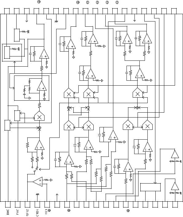
• IC102 (LA9247T) : RF Amplifier IC
I-V converts and amplifies the signal received from the pick-up and then applies to DSP part of onechip IC (IC501).
Block Diagram
|
PH |
BH |
VCC1 |
RFSM |
RHLD |
GND2 |
|
EQS |
FEEL |
FE |
CSS |
TE |
TS |
GHS |
VCC2 |
LDON |
FBAL |
TBAL |
SGC |
|
36 |
35 |
34 |
33 |
32 |
31 |
|
30 |
29 |
28 |
27 |
26 |
25 |
24 |
23 |
22 |
21 |
20 |
19 |
PH-control |
7-mode |
BH |
|
|
|
|
|
|
|
|
|
VREF2 |
|
|
|
|
|
|
|
|
PH |
|
|
|
|
VREF |
|
|
VREF2 |
|
|
|
|
|
VREF2 |
|
VREF2 |
|
|
|
|
EQ-control |
7-mode |
VREF |
VREF |
|
|
|
|
|
|
VREF |
|
|
|
|
VREF |
|
|
|
|
PH |
|
|
|
|
|
|
|
|
|
|
|
|
|
|
|
|
|
|
BH |
|
|
|
|
|
|
|
|
|
|
|
|
|
|
|
|
|
|
|
|
|
|
|
|
|
|
|
|
|
|
|
|
VREF2 |
|
|
|
|
|
|
|
|
|
|
|
|
|
|
|
|
|
VREF |
|
|
|
|
|
|
|
|
|
|
|
|
VREF |
|
|
|
|
VREF |
|
|
|
|
|
|
VREF |
5V |
|
|
|
|
|
|
|
VREF |
|
|
|
|
|
|
|
|
VREF |
|
|
|
|
|
|
|
|
|
|
|
|
|
|
|
|
|
2.5V |
|
A P C |
1.65V |
3.3V |
||
|
1 |
2 |
3 |
4 |
5 |
6 |
7 |
8 |
9 |
10 |
11 |
12 |
13 |
14 |
15 |
16 |
17 |
18 |
|
|
|
|
|
|
|
VCC3 |
3.3V |
A |
B |
C |
D |
REFI |
VREF |
E |
F |
LDD |
LDS |
VREF2 |
REFI2 |
11
 Loading...